C l o c k DA4601 2 4 6 - B i t 1 2 1 4 6bit Digital Step Attenuator ... · 2 t Rev. 0.4 eRex...
15
1 Preliminary Datasheet Rev. 0.4 BeRex ●website: www.berex.com ●email: [email protected] Specificaons and informaon are subject to change and products may be disconnued without noce. BeRex is a trademark of BeRex. All other trademarks are the property of their respecve owners. © 2018 BeRex 6bit Digital Step Aenuator 1MHz– 4GHz BDA4601 Figure 1. Funconal Block Diagram Device Features Figure 2. Package Type 20-lead 4x4 mm QFN • QFN 4x4mm 20 pin package • Serial & 6 bit Parallel Interface • 31.5 dB Control Range 0.5 dB step • No posive glitch • 2.7 V to 5.5 V supply • 1.8 V or 3.3 V control logic • Any bit Aenuaon Error < ±0.6 dB up to 3GHz • Low Inseron Loss 0.8dB @ 1MHz 0.9 dB @ 1GHz 1.3 dB @ 2GHz 1.6 dB @ 3GHz • High linearity IIP3 > +52 dBm • Input 0.1dB Compression (P0.1dB) 34dBm • Programming modes - Direct parallel - Latched parallel - Serial • Support funcon power up state selecon with PUP1,2 pin • Stable Integral Non-Linearity over temperature • Low Current Consumpon 150 μA typical • -40 °C to +105 °C operang temperature • ESD rang : Class2 (2KV HBM) Applicaon • Cellular Base staon/Repeater Infrastructure • Digital Pre-Distoron • Point to Point • Test Equipment and sensors • Military Wireless system • Cable Infrastructure • General purpose Wireless Product Descripon The BDA4601 is a 50Ω digital step aenuator model which provides adjustable aenuaon from 0 to 31.5 dB in 0.5 dB steps. The control is a 6-bit serial interface and parallel interface. Covering 1MHz to 4.0 GHz, the inseron loss is less than 1.5 dB typi- cal. And Offering the High linearity, low power consumpon, and low inseron loss. The device features safe state transions with No posive Glitch tech- nology. and is opmized for excellent step accuracy The RF input and output are internally matched to 50 Ω and do not require any external matching components. The design is bidirecon- al; therefore, the RF input and output are interchangeable. BDA4601 also features an external negave supply opon. This DSA does not require blocking capacitors. If DC is presented at the RF port, add a blocking capacitor. 1 D5 2 3 4 5 6 7 8 9 10 11 12 13 14 15 16 17 18 19 20 RF1 SERIN Clock LE VDD PUP 1 PUP 2 V DD GND GND VSS_EXT/GND P/S RF2 D4 D 3 D 2 GND D 1 D 0 6-Bit Digital Step Attenuator Serial/Parallel Control Logic Interface
Transcript of C l o c k DA4601 2 4 6 - B i t 1 2 1 4 6bit Digital Step Attenuator ... · 2 t Rev. 0.4 eRex...

1
Pre
limin
ary
Dat
ash
eet
Rev. 0.4
BeRex website: www.berex.com email: [email protected]
Specifications and information are subject to change and products may be discontinued without notice. BeRex is a trademark of BeRex.
All other trademarks are the property of their respective owners. © 2018 BeRex
6bit Digital Step Attenuator 1MHz– 4GHz
BDA4601
Figure 1. Functional Block Diagram Device Features
Figure 2. Package Type
20-lead 4x4 mm QFN
• QFN 4x4mm 20 pin package
• Serial & 6 bit Parallel Interface
• 31.5 dB Control Range 0.5 dB step
• No positive glitch
• 2.7 V to 5.5 V supply
• 1.8 V or 3.3 V control logic
• Any bit Attenuation Error < ±0.6 dB up to 3GHz
• Low Insertion Loss 0.8dB @ 1MHz 0.9 dB @ 1GHz 1.3 dB @ 2GHz 1.6 dB @ 3GHz
• High linearity IIP3 > +52 dBm
• Input 0.1dB Compression (P0.1dB) 34dBm
• Programming modes - Direct parallel - Latched parallel - Serial
• Support function power up state selection with PUP1,2 pin
• Stable Integral Non-Linearity over temperature
• Low Current Consumption 150 μA typical
• -40 °C to +105 °C operating temperature
• ESD rating : Class2 (2KV HBM)
Application
• Cellular Base station/Repeater Infrastructure
• Digital Pre-Distortion
• Point to Point
• Test Equipment and sensors
• Military Wireless system
• Cable Infrastructure
• General purpose Wireless
Product Description
The BDA4601 is a 50Ω digital step attenuator model which provides adjustable attenuation from 0 to 31.5 dB in 0.5 dB steps. The control is a 6-bit serial interface and parallel interface. Covering 1MHz to 4.0 GHz, the insertion loss is less than 1.5 dB typi-cal. And Offering the High linearity, low power consumption, and low insertion loss. The device features safe state transitions with No positive Glitch tech-nology. and is optimized for excellent step accuracy The RF input and output are internally matched to 50 Ω and do not require any external matching components. The design is bidirection-al; therefore, the RF input and output are interchangeable. BDA4601 also features an external negative supply option.
This DSA does not require blocking capacitors. If DC is presented at the RF port, add a blocking capacitor.
1D5
2
3
4
5
6 7 8 9 10
11
12
13
14
15
1617181920
RF1
SERIN
Clock
LE
VD
D
PUP1
PUP2
VD
D
GN
D
GND
VSS_EXT/GND
P/S
RF2
D4
D3
D2
GN
D
D1
D0
6-BitDigital Step Attenuator
Serial/ParallelControl Logic Interface

2
Pre
limin
ary
Dat
ash
eet
Rev. 0.4
BeRex website: www.berex.com email: [email protected]
Specifications and information are subject to change and products may be discontinued without notice. BeRex is a trademark of BeRex.
All other trademarks are the property of their respective owners. © 2018 BeRex
6bit Digital Step Attenuator 1MHz– 4GHz
BDA4601
1. Device performance _ measured on a BeRex Evaluation board Kit at 25°C, 50 Ω system, VDD=+3.3V 2. All data has PCB insertion loss de-embedded
Table 1. Electrical Specifications1
Parameter Condition Frequency Min Typ Max Unit
Operational Frequency Range 1 4000 MHz
Insertion Loss2 Attenuation = 0dB
1MHz - 1GHz 0.8 0.9 dB
> 1 - 2GHz 1.1 1.3 dB
> 2 - 3GHz 1.3 1.6 dB
> 3 - 4GHz 2.3 2.8 dB
Attenuation
Range 0.5dB step 0 - 31.5 dB
Accuracy Any bit or bit combination
1MHz - 1GHz ±(0.15 + 1% of attenuation state)
dB > 1 - 2.2GHz ±(0.15 + 2% of attenuation state)
> 2.2 - 3GHz ±(0.15 + 5% of attenuation state)
> 3 - 4GHz ±(0.15 + 8% of attenuation state)
Return loss
Input Return Loss
Attenuation = 0dB
1 - 2GHz 24
dB > 2 - 4GHz 16
Output Return Loss
1 - 2GHz 22
> 2 - 4GHz 15
Relative Phase Attenuation = 0dB
1GHz 11
degree 2GHz 26
3GHz 30
4GHz 48
Input Linearity
Input 0.1dB Compression
point Attenuation = 0dB 2140MHz 34 dBm
Input IP3 Pin= +5dBm/tone
f = 10KHz
Attn=0.0dB RFin =RF1
1950MHz
52
dBm Attn=0.0dB RFin =RF2 56
Attn=15.5dB RFin =RF1 57
Attn=15.5dB RFin =RF2 52
Switching time 50% CTRL to 90% or 10% RF 500 800 ns
Supply Current
Normal Mode 150 180 μA
Bypass Mode 50 80 μA
Negative supply Current -40 -16 μA

3
Pre
limin
ary
Dat
ash
eet
Rev. 0.4
BeRex website: www.berex.com email: [email protected]
Specifications and information are subject to change and products may be discontinued without notice. BeRex is a trademark of BeRex.
All other trademarks are the property of their respective owners. © 2018 BeRex
6bit Digital Step Attenuator 1MHz– 4GHz
BDA4601
Table 3. Absolute Maximum Ratings
Operation of this device above any of these parameters may result in permanent damage. 1 HBM : Human Body Model (JEDEC JESD22-A114) 2 CDM : Charged Device Model (JEDEC JESD22-C101)
1 Normal mode : connect pin 12 to GND to enable internal negative voltage generator 2 Bypass mode : Do not want to use negative voltage generator, supply a negative voltage to Vss_EXT(Pin12) for bypass and disable internal negative voltage generator.
Table 2. Recommended operating Condition
Parameter Symbol Condition Min Typ Max Unit
Supply Voltages
Normal Mode1 Supply Voltage VDD 2.7 5.5 V
Bypass Mode2 Supply Voltage VDD 2.7 5.5 V
Negative supply Voltage VSS_EXT -2.7 -2.5 -2.4 V
Digital Control Input
Normal Mode or
Bypass Mode
Input Voltage VCTL P/S, CLK, SERIN, LE, D0-D5, PUP1,PUP2
High VCTLH VDD=3.3V/5V 1.17 3.6 V
Low VCTLL VDD=3.3V/5V 0 0.6 V
Operating Temperature Range Tcase Exposed Paddle -40 105 ˚C
RF CW Input Power PIN_CW RF1 or RF2 24 dBm
Impedance ZLoad Single ended 50 Ω
Parameter Symbol Min Typ Max Unit
Supply Voltage VDD -0.3 5.5 V
Digital input voltage VCTL -0.3 3.6 V
Maximum input power PIN_CWMAX 34 dBm
Temperature
Juction TJ 140
Storage TST -65 150
Reflow TR 260
ESD Sensitivity HBM1 ESDHBM
2000 (Class 2)
V
CDM2 ESDCDM 500
(Class C2) V
4
Pre
limin
ary
Dat
ash
eet
Rev. 0.4
BeRex website: www.berex.com email: [email protected]
Specifications and information are subject to change and products may be discontinued without notice. BeRex is a trademark of BeRex.
All other trademarks are the property of their respective owners. © 2018 BeRex
6bit Digital Step Attenuator 1MHz– 4GHz
BDA4601
Table 4. Pin Description
Figure 3. Pin Configuration(Top View)
* Device is RF Bi -Directional
Pin Pin name Description
1 D5 Parallel Control Voltage Inputs, Attenuation control bit 16dB
2 RF11 RF1 port (Attenuator RF Input) This pin can also be used as an output because the design is bidirectional. RF1 is dc-coupled and matched to 50 Ω
3 SERIN Serial interface data input
4 CLK Serial interface clock input
5 LE Latch Enable input
6 VDD Power Supply (nominal 3.3V)
7 PUP1 Power-Up State Selection Bits. These pins set the attenuation value at power-up (see Table 11). There is no internal pull-up or pull-
down resistor on these pins; therefore, they must always be kept at a valid logic level (VCTLH or VCTLL) and not be left floating 8 PUP2
9 VDD Supply voltage (nominal 3.3V)
12 VSS_EXT 2/ GND External VSS negative voltage control or ground
Do not want to use negative voltage supply, These pins must be connected to ground (GND, Default setting is GND)
13 P/S Parallel/Serial Mode Select. For parallel mode operation, set this pin to low. For serial mode operation, set this pin to High.
14 RF21 RF2 port (Attenuator RF Output.) This pin can also be used as an input because the design is bidirectional. RF2 is dc-coupled and matched to 50 Ω.
15 D4 Parallel Control Voltage Inputs, Attenuation control bit 8dB
16 D3 Parallel Control Voltage Inputs, Attenuation control bit 4dB
17 D2 Parallel Control Voltage Inputs, Attenuation control bit 2dB
19 D1 Parallel Control Voltage Inputs, Attenuation control bit 1dB
20 D0 Parallel Control Voltage Inputs, Attenuation control bit 0.5dB
Pad GND Exposed pad: The exposed pad must be connected to ground for proper operation
10,11,18 GND Ground, These pins must be connected to ground
1D5
Exposed Pad
2
3
4
5
6 7 8 9 10
11
12
13
14
15
1617181920
RF1
SERIN
Clock
LE
VD
D
PUP1
PUP2
VD
D
GN
D
GND
VSS_EXT/GND
P/S
RF2
D4
D3
D2
GN
D
D1D0
Note: 1. RF pins 2 and 14 must be at 0V DC. The RF pins do not require DC blocking capacitors for proper Operation if the 0V DC requirement is met
2. Connect VssEXT (pin 12, VssEXT = GND) to enable internal negative voltage generator

5
Pre
limin
ary
Dat
ash
eet
Rev. 0.4
BeRex website: www.berex.com email: [email protected]
Specifications and information are subject to change and products may be discontinued without notice. BeRex is a trademark of BeRex.
All other trademarks are the property of their respective owners. © 2018 BeRex
6bit Digital Step Attenuator 1MHz– 4GHz
BDA4601
Programming Options
Figure 4. Serial Mode Resister Timing Diagram
Table 8. Truth Table for Serial Control Word
BDA4601 can be programmed using either the parallel or serial inter-face, which is selectable via P/S pin(Pin13). Serial mode is selected by floating P/S or pulling it to a voltage logic LOW and parallel mode is selected by setting P/S to logic low
Serial Control Mode The serial interface is a 6 bit shift register to shift in the data MSB (D5) first. When serial programming is used, all the parallel control input pins (1, 15, 16, 17, 19, 20) must be grounded. It is controlled by three CMOS-compatible signals: SERIN, Clock, and Latch Enable (LE).
Table 5. 6-Bit Serial Word Sequence
D5 Attenuation 16dB Control Bit
D4 Attenuation 8dB Control Bit
D3 Attenuation 4dB Control Bit
D2 Attenuation 2dB Control Bit
D1 Attenuation 1dB Control Bit
D0 Attenuation 0.5dB Control Bit
Table 7. Serial Interface Timing Specifications
Symbol Parameter Min Typ Max Unit
fClk Serial data clock frequency 10 MHz
tSCK Minimum serial period 70
tSS Serial Data setup time 10
tSH Serial Data hold time 10
tLN LE setup time 10
tLEW Minimum LE pulse width 30
tLES Minimum LE pulse spacing 600
The BDA4601 has a 3-wire serial peripheral interface (SPI): serial data input (Data), clock (CLK), and latch enable (LE). The serial control inter-face is activated when P/S is set to HIGH. In serial mode, the 6-bit Data is clocked MSB first on the rising CLK edges into the shift register and then LE must be toggled High to latch the new attenuation state into the device. LE must be set to low to clock new 6-bit data into the shift register because CLK is masked to prevent the attenuator value from changing if LE is kept High (see Figure 4 and Table 8).
Digital Control Input
Attenuation D5 D4 D3 D2 D1 D0
(MSB) (LSB) (dB)
LOW LOW LOW LOW LOW LOW 0 (Reference)
LOW LOW LOW LOW LOW HIGH 0.5
LOW LOW LOW LOW HIGH LOW 1
LOW LOW LOW HIGH LOW LOW 2
LOW LOW HIGH LOW LOW LOW 4
LOW HIGH LOW LOW LOW LOW 8
HIGH LOW LOW LOW LOW LOW 16
HIGH HIGH HIGH HIGH HIGH HIGH 31.5
P/S Control Mode
LOW Parallel
HIGH Serial
Table 6. Mode Selection
D5X X D[5:0]NEXT WORD XD4 D3 D2 D1 D0
X
tSH
tSStSCK
tLNtLEW
tLES
MSB[FIRST IN]
LSB[LAST IN]
P/S
SERIAL IN
CLK
LE

6
Pre
limin
ary
Dat
ash
eet
Rev. 0.4
BeRex website: www.berex.com email: [email protected]
Specifications and information are subject to change and products may be discontinued without notice. BeRex is a trademark of BeRex.
All other trademarks are the property of their respective owners. © 2018 BeRex
6bit Digital Step Attenuator 1MHz– 4GHz
BDA4601
Figure 5. Latched Parallel Mode Timing Diagram
Parallel Control Mode The BDA4601 has six digital control inputs, D0 (LSB) to D5 (MSB), to select the desired attenuation state in parallel mode, as shown in Table 9. The parallel control interface is activated when P/S is set to low. There are two modes of parallel operation: direct parallel and latched parallel Direct Parallel Mode The LE pin must be kept LOW. The attenuation state is changed by the control voltage inputs (D0 to D5) directly. This mode is ideal for man-ual control of the attenuator. In this mode the device will immediate-ly react to any voltage changes to the parallel control pins [pins 1, 15, 16, 17,19, 20]. Use direct parallel mode for the fastest settling time. Latched Parallel Mode The LE pin must be kept low when changing the control voltage inputs (D0 to D5) to set the attenuation state. When the desired state is set, LE must be toggled LOW to transfer the 6-bit data to the bypass switches of the attenuator array, and then toggled low to latch the change into the device until the next desired attenuation change (see Figure 5 and Table 9).
Table 10. Parallel Interface Timing Specifications
Symbol Parameter Min Typ Max Unit
tLEW Minimum LE pulse width 10 ns
tPH Data hold time from LE 10 ns
tPS Data setup time to LE 10 ns
X
tPHtPS
P/S
Parallel IN
LE
XD[5:0]
PARALLELCONTROL
tLEW
X
D0 D1 D2 D3 D4 D5 Attenuation State LE P/S
LOW LOW LOW LOW LOW LOW Reference Loss HIGH LOW
HIGH LOW LOW LOW LOW LOW 0.5dB HIGH LOW
LOW HIGH LOW LOW LOW LOW 1dB HIGH LOW
LOW LOW HIGH LOW LOW LOW 2dB HIGH LOW
LOW LOW LOW HIGH LOW LOW 4dB HIGH LOW
LOW LOW LOW LOW HIGH LOW 8dB HIGH LOW
LOW LOW LOW LOW LOW HIGH 16dB HIGH LOW
HIGH HIGH HIGH HIGH HIGH HIGH 31.5dB HIGH LOW
Table 9. Truth Table for the Parallel Control Word
Table 11. PUP Truth Table for Parallel Control Mode
Power-UP Interface The BDA4601 uses the PUP1 and PUP2 control voltage inputs to set the attenuation value to a known value at power-up before the initial control data word is provided in parallel mode. Power-up Control for Parallel Mode (P/S=LOW) When the attenuator powers up with LE set to low, the state of PUP1 and PUP2 determines the power-up state of the device per the truth table shown in Table 11. Power-up Control for Serial Mode (P/S=HIGH) When the attenuator powers up in Serial mode, the six digital control inputs are set to whatever data is present on the six parallel data inputs (D0 to D5, Refer to Table 12). This allows any one of the 64 attenuation settings to be specified as the power-up state.
Attenuation state P/S LE PUP1 PUP2
31.5 dB LOW LOW HIGH HIGH
16 dB LOW LOW HIGH LOW
8 dB LOW LOW LOW HIGH
Reference Loss LOW LOW LOW LOW
Defined by C0.5-C16 LOW HIGH Don’t Care Don’t Care
Attenuation State P/S D0 D1 D2 D3 D4 D5
Reference Loss HIGH LOW LOW LOW LOW LOW LOW
0.5dB HIGH HIGH LOW LOW LOW LOW LOW
1dB HIGH LOW HIGH LOW LOW LOW LOW
2dB HIGH LOW LOW HIGH LOW LOW LOW
4dB HIGH LOW LOW LOW HIGH LOW LOW
8dB HIGH LOW LOW LOW LOW HIGH LOW
16dB HIGH LOW LOW LOW LOW LOW HIGH
20dB HIGH LOW LOW LOW HIGH LOW HIGH
24dB HIGH LOW LOW LOW LOW HIGH HIGH
31.5dB HIGH HIGH HIGH HIGH HIGH HIGH HIGH
Table 12. PUP Truth Table for Serial Control Mode

7
Pre
limin
ary
Dat
ash
eet
Rev. 0.4
BeRex website: www.berex.com email: [email protected]
Specifications and information are subject to change and products may be discontinued without notice. BeRex is a trademark of BeRex.
All other trademarks are the property of their respective owners. © 2018 BeRex
6bit Digital Step Attenuator 1MHz– 4GHz
BDA4601
Figure 6. Insertion Loss vs. Frequency over Major Attenuation States Figure 7 Insertion Loss vs. Frequency over Temperature
Figure 8. Input Return Loss vs. Frequency over Major Attenuation States
Figure 10. Output Return Loss vs. Frequency over Major Attenuation States
Figure 9. Input Return Loss vs. Frequency over Temperature
Figure 11. Output Return Loss vs. Frequency over Temperature
Typical Performance Data @ 25°and VDD = 3.3V, All data has PCB insertion loss de-embedded, unless otherwise noted
Typical RF Performance Plot - BDA4601 EVK - PCB
-4.0
-3.5
-3.0
-2.5
-2.0
-1.5
-1.0
-0.5
0.0
0 1 2 3 4
Inse
rtio
n Lo
ss [
dB]
Frequency [GHz]
+25°C
-40°C
+105°C
-40
-35
-30
-25
-20
-15
-10
-5
0
0 1 2 3 4
Inse
rtio
n L
oss
[d
B]
Frequency [GHz]
0dB 0.5dB
1dB 2dB
4dB 8dB
16dB 31.5dB
-60
-50
-40
-30
-20
-10
0
0 1 2 3 4
Inpu
t R
etur
n Lo
ss [
dB]
Frequency [GHz]
0dB 0.5dB
1dB 2dB
4dB 8dB
16dB 31.5dB
-60
-50
-40
-30
-20
-10
0
0 1 2 3 4
Inpu
t R
etur
n Lo
ss [
dB]
Frequency [GHz]
+25°C
-40°C
+105°C
-60
-50
-40
-30
-20
-10
0
0 1 2 3 4
Out
put
Ret
urn
Loss
[dB
]
Frequency [GHz]
0dB 0.5dB
1dB 2dB
4dB 8dB
16dB 31.5dB
-60
-50
-40
-30
-20
-10
0
0 1 2 3 4
Out
put
Ret
urn
Loss
[dB
]
Frequency [GHz]
+25°C
-40°C
+105°C

8
Pre
limin
ary
Dat
ash
eet
Rev. 0.4
BeRex website: www.berex.com email: [email protected]
Specifications and information are subject to change and products may be discontinued without notice. BeRex is a trademark of BeRex.
All other trademarks are the property of their respective owners. © 2018 BeRex
6bit Digital Step Attenuator 1MHz– 4GHz
BDA4601
Figure 12. Attenuation Error vs. Attenuation State over Frequency Figure13. Attenuation Error vs. Major Frequency over Attenuation States
Figure 14. Step Error vs Attenuation State over Frequency
Figure 16. Relative Phase vs. Attenuation State over Frequency
Figure 15. Actual Attenuation vs Ideal Attenuation over Frequency
Figure 17. Attenuation Error at 100Mhz vs Temperature over Attenuation State
Typical Performance Data @ 25°and VDD = 3.3V, All data has PCB insertion loss de-embedded, unless otherwise noted
Typical RF Performance Plot - BDA4601 EVK - PCB
-3
-2
-1
0
1
2
3
0 1 2 3 4
Att
en
ua
tio
n E
rro
r [d
B]
Frequency [GHz]
0.5dB 1dB
2dB 4dB
8dB 16dB
31.5dB
-10
0
10
20
30
40
50
60
0 1 2 3 4
Rel
ativ
e Ph
ase
[deg
ree]
Frequency [GHz]
0.5dB 1dB
2dB 4dB
8dB 16dB
31.5dB
-2
-1.5
-1
-0.5
0
0.5
1
1.5
2
0 5 10 15 20 25 30
Att
en
ua
tio
n E
rro
r [d
B]
Attenuation Setting [dB]
+25°C
-40°C
+105°C
-3
-2
-1
0
1
2
3
0 5 10 15 20 25 30
Att
enua
tion
Err
or [
dB]
Attenuation Setting [dB]
10MHz100MHz1GHz2GHz3GHz4GHz
-1
-0.8
-0.6
-0.4
-0.2
0
0.2
0.4
0.6
0.8
1
0 5 10 15 20 25 30
Step
Att
enua
tio
n Er
ror
[dB]
Attenuation Setting [dB]
10MHz100MHz1GHz2GHz3GHz4GHz
0
5
10
15
20
25
30
35
0 5 10 15 20 25 30
Att
enua
tion
Err
or [
dB]
Attenuation Setting [dB]
10MHz100MHz1GHz2GHz3GHz4GHz
9
Pre
limin
ary
Dat
ash
eet
Rev. 0.4
BeRex website: www.berex.com email: [email protected]
Specifications and information are subject to change and products may be discontinued without notice. BeRex is a trademark of BeRex.
All other trademarks are the property of their respective owners. © 2018 BeRex
6bit Digital Step Attenuator 1MHz– 4GHz
BDA4601
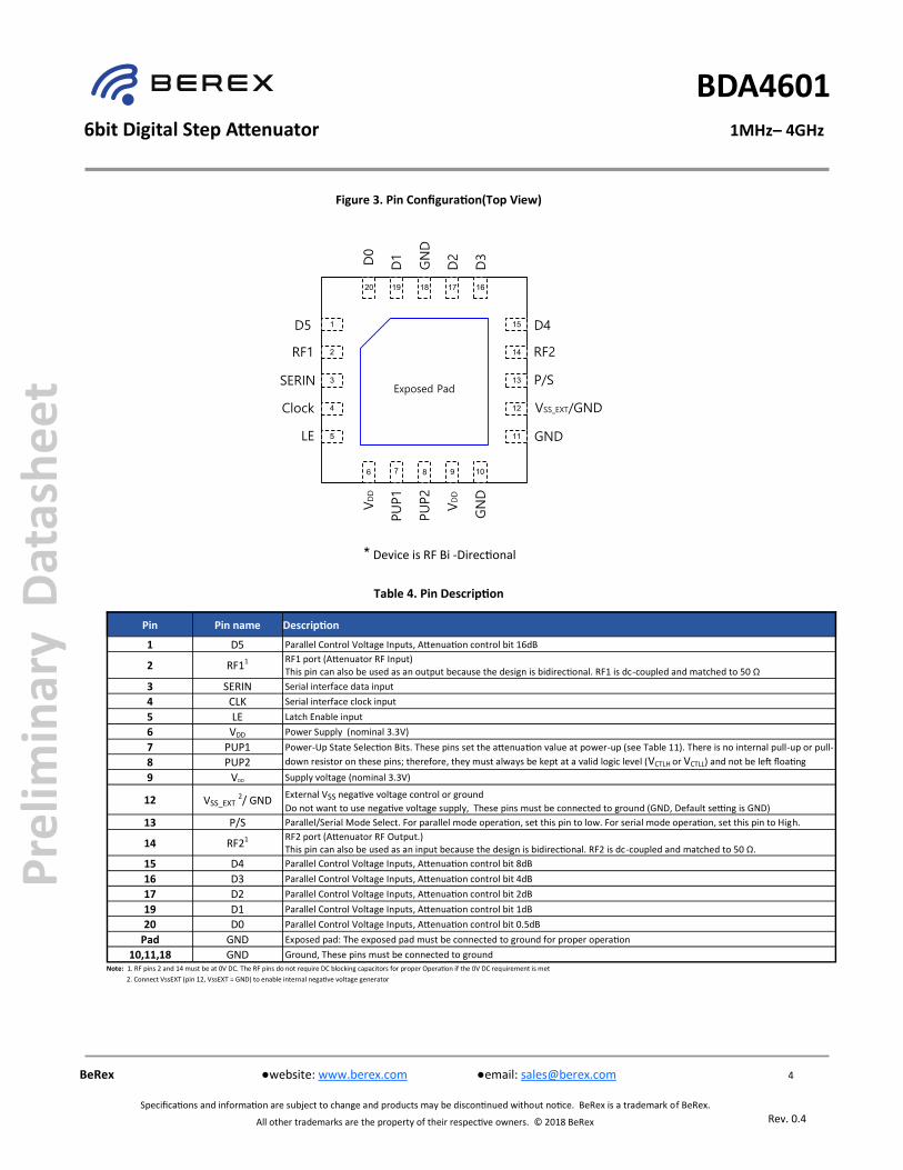
Figure 18. Attenuation Error at 1Ghz vs Temperature over Attenuation State Figure 19. Attenuation Error at 2Ghz vs Temperature over Attenuation State
Figure 20. Attenuation Error at 3Ghz vs Temperature over Attenuation State
Figure 22. Compression3 at 2.14GHz vs. Input Power over Major Attenuation state
Figure 21. Attenuation Error at 4Ghz vs Temperature over Attenuation State
Figure 23. Compression at 2.14GHz and Minimum Attenuation State1 vs. Input Power
over Temperature
Typical Performance Data @ 25°and VDD = 3.3V, All data has PCB insertion loss de-embedded, unless otherwise noted
Typical RF Performance Plot - BDA4601 EVK - PCB
Note: 1. Minimum Attenuation state means that the attenuation setting is 0dB. 2. Maximum Attenuation state means that the attenuation setting is 31.5dB. 3. Input 0.1dB Compression
-2
-1.5
-1
-0.5
0
0.5
1
1.5
2
0 5 10 15 20 25 30
Att
en
ua
tio
n E
rro
r [d
B]
Attenuation Setting [dB]
+25°C
-40°C
+105°C
-2
-1.5
-1
-0.5
0
0.5
1
1.5
2
0 5 10 15 20 25 30
Att
en
ua
tio
n E
rro
r [d
B]
Attenuation Setting [dB]
+25°C
-40°C
+105°C
-2
-1.5
-1
-0.5
0
0.5
1
1.5
2
0 5 10 15 20 25 30
Att
en
ua
tio
n E
rro
r [d
B]
Attenuation Setting [dB]
+25°C
-40°C
+105°C
-4
-3
-2
-1
0
1
2
0 5 10 15 20 25 30
Att
en
ua
tio
n E
rro
r [d
B]
Attenuation Setting [dB]
+25°C
-40°C
+105°C
-0.5
-0.4
-0.3
-0.2
-0.1
0
0.1
0.2
0.3
0.4
0.5
20 22 24 26 28 30 32 34
Com
pres
sion
[dB
]
Input Power[dBm]
+25°C
-40°C
+105°C
-0.5
-0.4
-0.3
-0.2
-0.1
0
0.1
0.2
0.3
0.4
0.5
20 22 24 26 28 30 32 34
Com
pres
sion
[dB
]
Input Power[dBm]
0dB
15.5dB
31.5dB

10
Pre
limin
ary
Dat
ash
eet
Rev. 0.4
BeRex website: www.berex.com email: [email protected]
Specifications and information are subject to change and products may be discontinued without notice. BeRex is a trademark of BeRex.
All other trademarks are the property of their respective owners. © 2018 BeRex
6bit Digital Step Attenuator 1MHz– 4GHz
BDA4601
Figure 24. Compression2 at 2.14GHz and Maximum Attenuation State1 vs. Input
Power over Temperature
Typical Performance Data @ 25°and VDD = 3.3V, All data has PCB insertion loss de-embedded, unless otherwise noted
Typical RF Performance Plot - BDA4601 EVK - PCB
Figure 25. IIP3 at 1.8GHz vs. Attenuation setting over Temperature
Figure 26. IIP3 at 1.95GHz vs. Attenuation setting over Temperature
Figure 28. IIP3 at 2.45GHz vs. Attenuation setting over Temperature
Figure 27. IIP3 at 2.15GHz vs. Attenuation setting over Temperature
Note: 1. Maximum Attenuation state means that the attenuation setting is 31.5dB.
2. Input 0.1dB Compression
-0.5
-0.4
-0.3
-0.2
-0.1
0
0.1
0.2
0.3
0.4
0.5
20 22 24 26 28 30 32 34
Com
pres
sion
[dB
]
Input Power[dBm]
+25°C
-40°C
+105°C
10
20
30
40
50
60
70
0.0 5.0 10.0 15.0 20.0 25.0 30.0
IIP
3 [
dB
]
Attenuation Setting [dB]
+25°C
-40°C
+105°C
10
20
30
40
50
60
70
0.0 5.0 10.0 15.0 20.0 25.0 30.0
IIP
3 [
dB
]
Attenuation Setting [dB]
+25°C
-40°C
+105°C
10
20
30
40
50
60
70
0.0 5.0 10.0 15.0 20.0 25.0 30.0
IIP
3 [
dB
]
Attenuation Setting [dB]
+25°C
-40°C
+105°C
10
20
30
40
50
60
70
0.0 5.0 10.0 15.0 20.0 25.0 30.0
IIP
3 [
dB
]
Attenuation Setting [dB]
+25°C
-40°C
+105°C
10
20
30
40
50
60
70
0.0 5.0 10.0 15.0 20.0 25.0 30.0
IIP
3 [
dB
]
Attenuation Setting [dB]
+25°C
-40°C
+105°C
Figure 28. IIP3 at 2.65GHz vs. Attenuation setting over Temperature

11
Pre
limin
ary
Dat
ash
eet
Rev. 0.4
BeRex website: www.berex.com email: [email protected]
Specifications and information are subject to change and products may be discontinued without notice. BeRex is a trademark of BeRex.
All other trademarks are the property of their respective owners. © 2018 BeRex
6bit Digital Step Attenuator 1MHz– 4GHz
BDA4601
BDA4601 Evaluation board Kit Description
Evaluation board Kit Introduction BDA4601 Evaluation Kit is made up of a combination of an RF board and an interface board The schematic of the BDA4601 evaluation RF board is shown in Figure 30. The BDA4601 evalu-ation RF board is constructed of a 4-layer material with a copper thickness of 0.7 mil on each layer. Every copper layer is separated with a dielectric material. The top dielectric material is 12 mil RO4003. The middle and bottom dielectric materials are FR-4, used for mechanical strength and overall board thickness of approximately 1.55mm. BDA4601 Evaluation INTERFACE board is assembled with a SP3T switches(D1~D6,LE), SP2T mechanical switch (P/S), and several header & switch.
Evaluation Board Programming Using USB Interface In order to evaluate the BDA4601 performance, the Application Software has to be installed on your computer. And The DSA application software GUI supports Latched Parallel and Serial
modes. software can be downloaded from BeRex’s website
Serial Control Mode
• Connect directly the Evaluation INTEFRACE board USB port(J3) to PC
• Set the direction of P<->S Switch to S direction
• Set the D0~D5,LE switch to the central position.
• Operate the 0~31.5dB attenuation state in GUI and then control the DSA
Latched Parallel Control Mode
• Connect directly the Evaluation INTEFRACE board USB port(J3) to PC
• Set the direction of P<->S Switch to P direction
• Set the D0~D5,LE switch to the middle position.
• Operate the 0~31.5dB attenuation state in GUI and then control the DSA
Direct Parallel Control Mode
• Set the direction of P<->S Switch to P direction
• Set LE switch to the LOW Position
• For the setting to attenuation state, D0~D5 switches can be combined in manually pro-gram, refer to Table 9.
Please refer to user manual for more detailed operation method of BDA4601 EVK.
Figure 30. BDA4601 EVK
12
Pre
limin
ary
Dat
ash
eet
Rev. 0.4
BeRex website: www.berex.com email: [email protected]
Specifications and information are subject to change and products may be discontinued without notice. BeRex is a trademark of BeRex.
All other trademarks are the property of their respective owners. © 2018 BeRex
6bit Digital Step Attenuator 1MHz– 4GHz
BDA4601
Figure 31. Evaluation Board Schematic Diagram for Parallel and Serial with PUP
Figure 33. Evaluation Board PCB Layer Information 50Ω
Figure 32. Evaluation Board PCB Layout Information 50Ω Table13. Bill of Material - Evaluation Board
No. Ref Des Part
Qty Value Description Remark
1 C1,C3,C5-C10 8 100pF CAP, 0402, CHIP Ceramic, ±0.25%
2 C2,C4 2 100nF CAP, 0402, CHIP Ceramic, ±0.25%
3 R1,R2 2 10k ohm RES, 0402, CHIP, ±5%
4 R3,R4 2 NC
5 R5,R6,R7,R16,R17 5 0 ohm RES, 0402, CHIP, ±5%
6 C41 1 10 uF TANTAL 3216 10UF 16V
7 J1,J2 2 CON SMA END LAUNCH
8 U1 1 Chip DSA, BDA4601 QFN4x4 24L
COPPER : 1oz(0.035mm), Top Layer
RO4003C : 0.305mm
COPPER : 1oz(0.035mm), GND, Inner Layer
COPPER : 1oz(0.035mm), Inner Layer
COPPER : 1oz(0.035mm), Bottom Layer
FR-4 : 0.36mm
Core FR-4 : 0.73mm
Finish
Thickn
ess : 1.5
5T
TOP
BOTTOM
RO4003C Er: 3.38
FR-4 Er: 4.5~4.8
FR-4 Er: 4.5~4.8
U1(BDA4601)
RF11
2
3
4
5
6 7 8 9 10
15
14
13
12
11
20 19 18 17 16
VDD
C8/CLK
C16/DATA
RF2
C4
C1
C2
C0.5
P/S
PUP1
PUP2
R1 10KR17
0 ohm
C41 10uF
C3 100nF
C2 100pF
C1 100pF
C10 100pF
C6 100pF
C7 100pF
C8 100pF
C9 100pF
R16 0 ohm
C4 100pF
C5 100nF
R3 NCR5 0 ohm
R6 0 ohm
R4 NC
R2 10K
VSS/GND
J1 J2
R7 0ohm
BDA4601 Evaluation board Kit Description
Note: 1. C2 and C3 should be placed near the device.

13
Pre
limin
ary
Dat
ash
eet
Rev. 0.4
BeRex website: www.berex.com email: [email protected]
Specifications and information are subject to change and products may be discontinued without notice. BeRex is a trademark of BeRex.
All other trademarks are the property of their respective owners. © 2018 BeRex
6bit Digital Step Attenuator 1MHz– 4GHz
BDA4601
Figure 34. Evaluation Board Schematic Diagram For Serial only
BDA4601 Evaluation board Kit Description
Note: 1. C2 and C3 should be placed near the device. 2. VDC(Fig35) is a 3.0V DC constant voltage supply for Power up control. When attenuator use only serial mode (Attenuation state 31.5dB)
U1(BDA4600)
RF11
2
3
4
5
6 7 8 9 10
15
14
13
12
11
20 19 18 17 16
VDD
CLK
DATA
RF2
P/S
C41 10uF
C3 100nF
C2 100pF
J1 J2
R7 0ohm
LE
Figure 35. Evaluation Board Schematic Diagram For Serial only & Power Up control
U1(BDA4600)
RF11
2
3
4
5
6 7 8 9 10
15
14
13
12
11
20 19 18 17 16
VDD
CLK
DATA
RF2
P/S
C41 10uF
C3 100nF
C2 100pF
J1 J2
R7 0ohm
LE
VDC

14
Pre
limin
ary
Dat
ash
eet
Rev. 0.4
BeRex website: www.berex.com email: [email protected]
Specifications and information are subject to change and products may be discontinued without notice. BeRex is a trademark of BeRex.
All other trademarks are the property of their respective owners. © 2018 BeRex
6bit Digital Step Attenuator 1MHz– 4GHz
BDA4601
Figure 36. Packing outline Dimension
Figure 37. Recommend Land Pattern
15
14
13
12
11
109876
1
2
3
4
5
16
17
18
19
20
4.40
2.20
2.20 4.40
0.5
Ф 0.25
0.5
0.75Pin No.1
0.25
0.5
15
Pre
limin
ary
Dat
ash
eet
Rev. 0.4
BeRex website: www.berex.com email: [email protected]
Specifications and information are subject to change and products may be discontinued without notice. BeRex is a trademark of BeRex.
All other trademarks are the property of their respective owners. © 2018 BeRex
6bit Digital Step Attenuator 1MHz– 4GHz
BDA4601
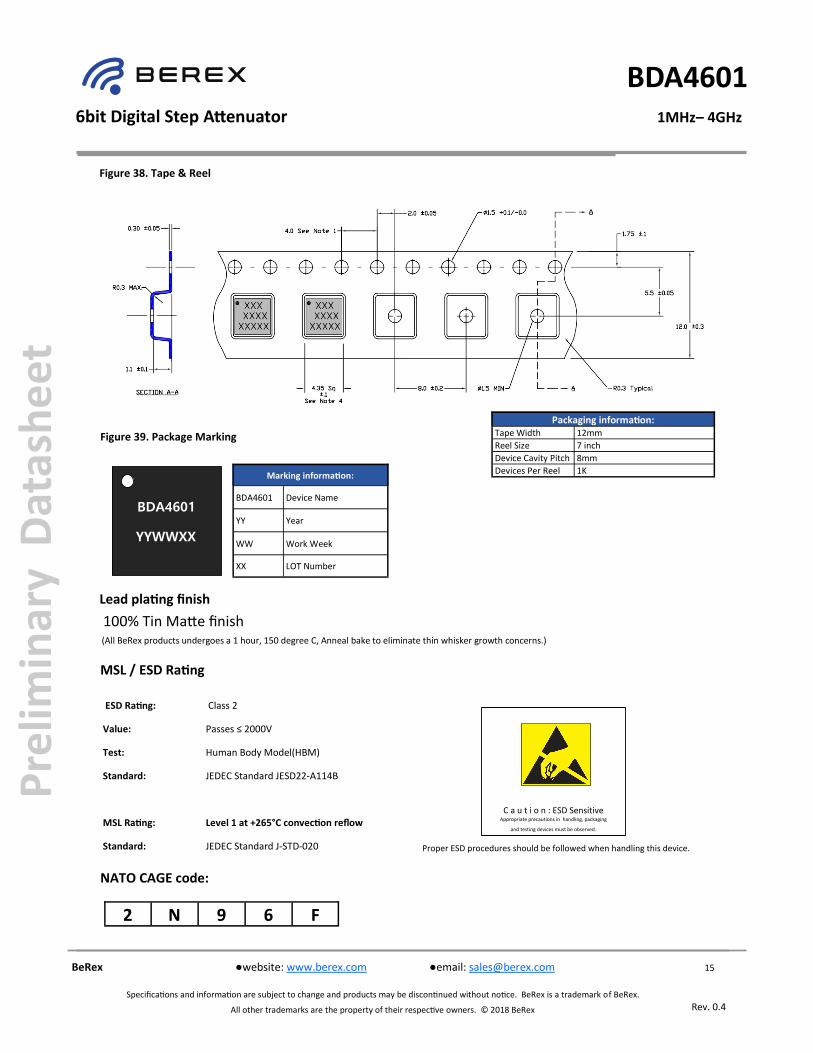
Figure 38. Tape & Reel
Lead plating finish
100% Tin Matte finish (All BeRex products undergoes a 1 hour, 150 degree C, Anneal bake to eliminate thin whisker growth concerns.)
MSL / ESD Rating
ESD Rating:
Value:
Test:
Standard:
MSL Rating:
Standard:
Class 2
Passes ≤ 2000V
Human Body Model(HBM)
JEDEC Standard JESD22-A114B
Level 1 at +265°C convection reflow
JEDEC Standard J-STD-020
NATO CAGE code:
2 N 9 6 F
Figure 39. Package Marking
BDA4601
YYWWXX
Packaging information: Tape Width 12mm
Reel Size 7 inch
Device Cavity Pitch 8mm
Devices Per Reel 1K Marking information:
BDA4601 Device Name
YY Year
WW Work Week
XX LOT Number
Proper ESD procedures should be followed when handling this device.
C a u t i o n : ESD SensitiveAppropriate precautions in handling, packaging
and testing devices must be observed.