
C. Hutchens Chap 5 ECEN 3313 Handouts 1 Chapter 5 Structure and Physical Operation I -V...
51
C. Hutchens Chap 5 ECEN 3313 Handouts 1 Chapter 5 • Structure and Physical Operation • I -V characteristics • MOSFET DC circuits • MOSFET amplifiers • Biasing MOSFETS • CMOS Inverter • High Frequency MOS model • SPICE MOSFET model parameters
-
Upload
archibald-fox -
Category
Documents
-
view
222 -
download
2
Transcript of C. Hutchens Chap 5 ECEN 3313 Handouts 1 Chapter 5 Structure and Physical Operation I -V...
C. Hutchens Chap 5 ECEN 3313 Handouts 1
Chapter 5
• Structure and Physical Operation
• I -V characteristics
• MOSFET DC circuits
• MOSFET amplifiers
• Biasing MOSFETS
• CMOS Inverter
• High Frequency MOS model
• SPICE MOSFET model parameters
C. Hutchens Chap 5 ECEN 3313 Handouts 2
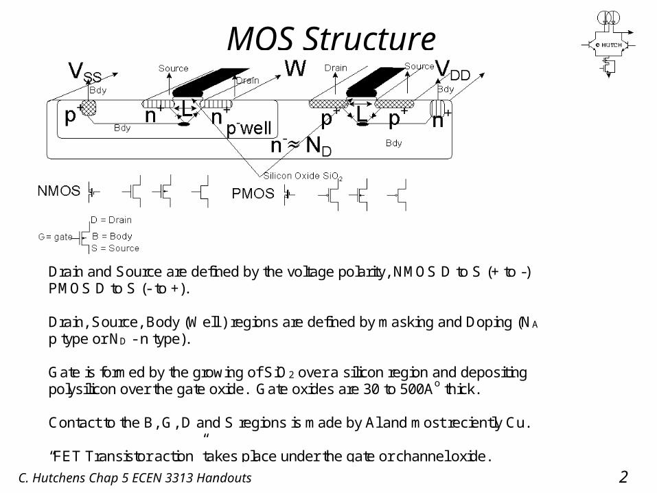
MOS Structure
Drain and Source are defined by the voltage polarity, NMOS D to S (+ to -)PMOS D to S (- to +).
Drain, Source, Body (Well ) regions are defined by masking and Doping (NA
p type or ND - n type).
Gate is formed by the growing of SiO2 over a silicon region and depositingpolysilicon over the gate oxide. Gate oxides are 30 to 500Ao thick.
Contact to the B, G, D and S regions is made by Al and most reciently Cu.
“FET Transistor action” takes place under the gate or channel oxide.
C. Hutchens Chap 5 ECEN 3313 Handouts 3
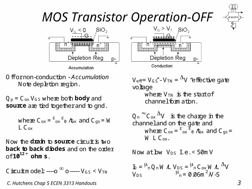
MOS Transistor Operation-OFF
Veff = VGS - VTN = V “effective gatevoltage”
where VTN is the start ofchannel formation.
Qn Cox V is the charge in thechannel and on the gate and
where Cox = ox 0 /tox and Cgs =W L Cox.
Now at low VDS I. e. < 50mV
ID = n Qn W/L VDS = n Cox W/L VVDS n = 0.06m2/V-S
Off or non-conduction - AccumulationNote depletion region.
Qp = Cox VGS where both body andsource are tied together and to gnd.
where Cox = ox 0 /tox and Cgs = WL Cox
Now the drain to source circuit is twoback to back diodes and on the orderof 1012 + ohms.
Circuit model: ----o o----- VGS < VTN
C. Hutchens Chap 5 ECEN 3313 Handouts 4
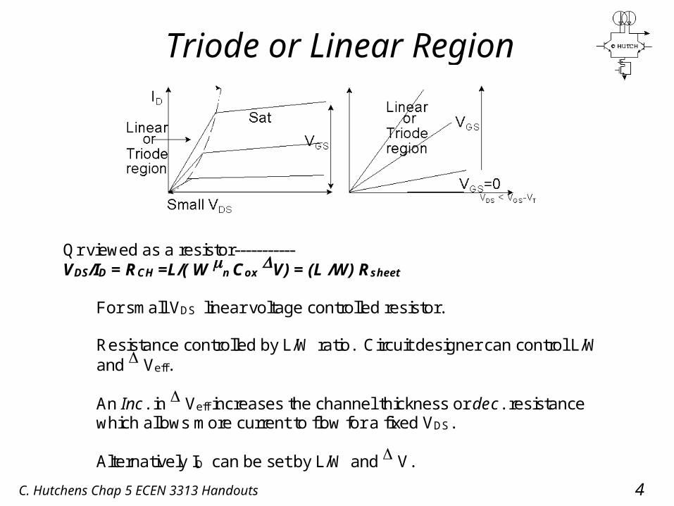
Triode or Linear Region
Qr viewed as a resistor-----------VDS/ID = RCH =L/( W n Cox V) = (L /W) Rsheet
For small VDS linear voltage controlled resistor.
Resistance controlled by L/W ratio. Circuit designer can control L/Wand Veff.
An Inc. in Veff increases the channel thickness or dec. resistancewhich allows more current to flow for a fixed VDS.
Alternatively ID can be set by L/W and V.
C. Hutchens Chap 5 ECEN 3313 Handouts 5
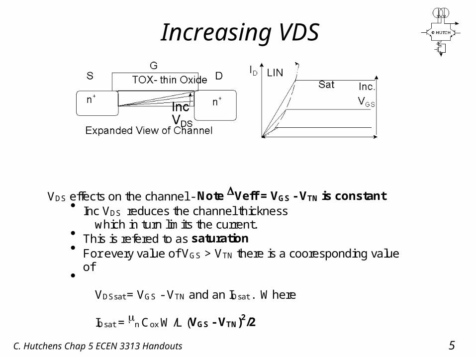
Increasing VDS
VDS effects on the channel - Note Veff = VGS - VTN is constantInc VDS reduces the channel thickness
which in turn limits the current.This is refered to as saturationFor every value of VGS > VTN there is a cooresponding value
of
VDSsat = VGS - VTN and an IDsat . Where
IDsat = n Cox W/L (VGS - VTN)2/2
C. Hutchens Chap 5 ECEN 3313 Handouts 6
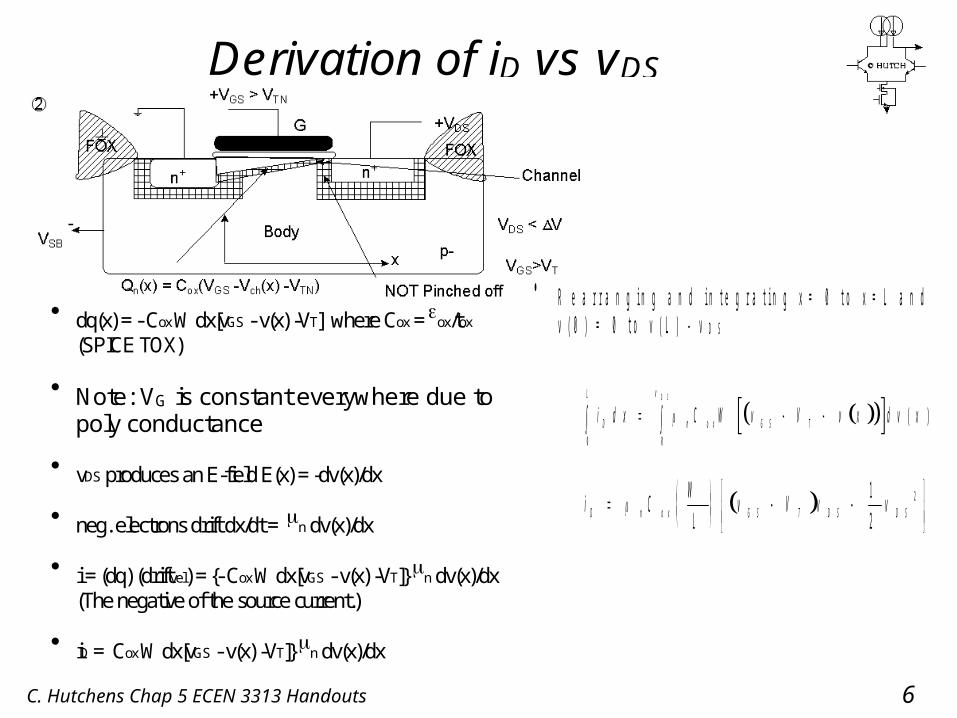
Derivation of iD vs vDS
dq(x) = - Cox W dx[vGS - v(x) -VT] where Cox = ox/tox
(SPICE TOX)
Note: VG is constant everywhere due topoly conductance
vDS produces an E-field E(x) = -dv(x)/dx
neg. electrons drift dx/dt = n dv(x)/dx
i = (dq) (driftvel) = {- Cox W dx[vGS - v(x) -VT]} n dv(x)/dx(The negative of the source current.)
iD = Cox W dx[vGS - v(x) -VT]} n dv(x)/dx
R e a r r a n g i n g a n d i n t e g r a t i n g x = 0 t o x = L a n dv ( 0 ) = 0 t o v ( L ) - v D S
i d x C W v V v x d v xD
L
n
v
o x G S T
D S
0 0 ( )
i CW
Lv V v vD n o x G S T D S D S
1
22
C. Hutchens Chap 5 ECEN 3313 Handouts 7
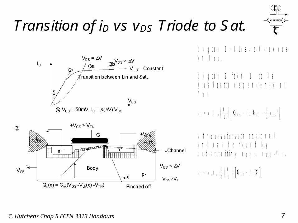
Transition of iD vs vDS Triode to Sat.
R e g i o n 1 - L i n e a r D e p e n c eo n V D S .
R e g i o n 2 f r o m 1 t o 3 aQ u a d r a t i c d e p e n c e n c e o nV D S
i CW
Lv V v vD n o x G S T D S D S
1
22
A t v D S s a t i D s a t i s r e a c h e da n d c a n b e f o u n d b ys u b s t i t u i t i n g v D S = v G S - V T .
i CW
Lv VD n o x G S T
1
22
C. Hutchens Chap 5 ECEN 3313 Handouts 8
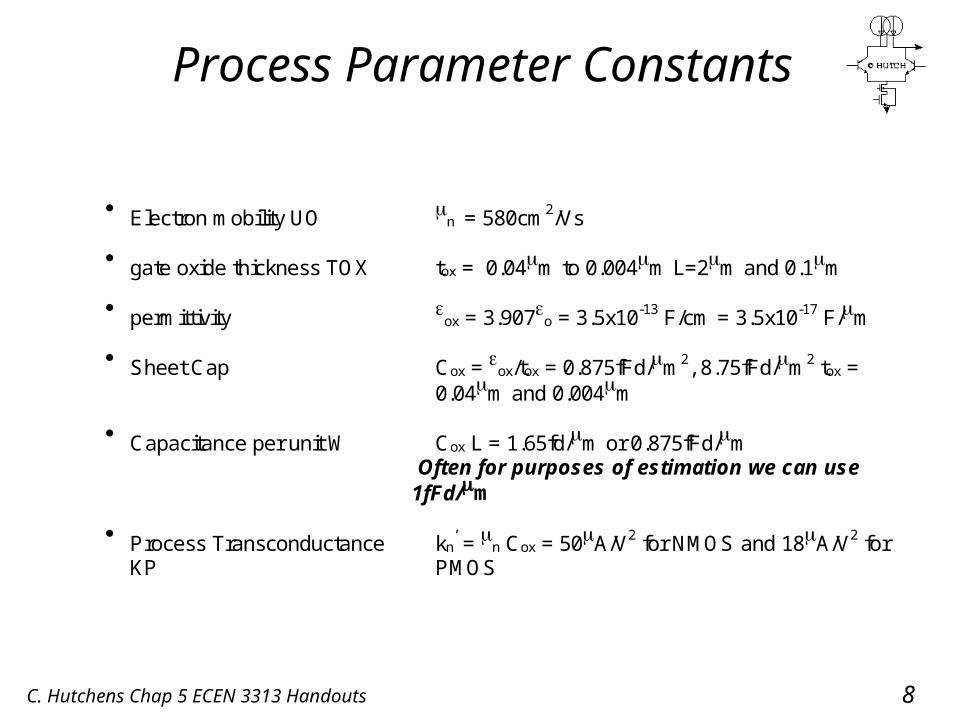
Process Parameter Constants
Electron mobility UO n = 580cm2/Vs
gate oxide thickness TOX tox = 0.04m to 0.004m L=2m and 0.1m
permittivity ox = 3.907o = 3.5x10⁻¹³ F/cm = 3.5x10⁻¹⁷ F/m
Sheet Cap Cox = ox/tox = 0.875fFd/m2, 8.75fFd/m2 tox = 0.04m and 0.004m
Capacitance per unit W Cox L = 1.65fd/m or 0.875fFd/m Often for purposes of estimation we can use
1fFd/m
Process Transconductance kn’ = n Cox = 50A/V2 for NMOS and 18A/V2 for
KP PMOS
C. Hutchens Chap 5 ECEN 3313 Handouts 9
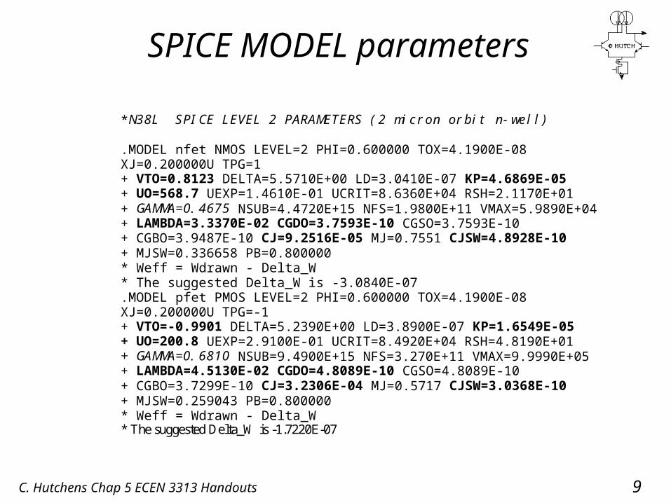
SPICE MODEL parameters
*N38L SPICE LEVEL 2 PARAMETERS (2 micron orbit n-well)
.MODEL nfet NMOS LEVEL=2 PHI=0.600000 TOX=4.1900E-08XJ=0.200000U TPG=1+ VTO=0.8123 DELTA=5.5710E+00 LD=3.0410E-07 KP=4.6869E-05+ UO=568.7 UEXP=1.4610E-01 UCRIT=8.6360E+04 RSH=2.1170E+01+ GAMMA=0.4675 NSUB=4.4720E+15 NFS=1.9800E+11 VMAX=5.9890E+04+ LAMBDA=3.3370E-02 CGDO=3.7593E-10 CGSO=3.7593E-10+ CGBO=3.9487E-10 CJ=9.2516E-05 MJ=0.7551 CJSW=4.8928E-10+ MJSW=0.336658 PB=0.800000* Weff = Wdrawn - Delta_W* The suggested Delta_W is -3.0840E-07.MODEL pfet PMOS LEVEL=2 PHI=0.600000 TOX=4.1900E-08XJ=0.200000U TPG=-1+ VTO=-0.9901 DELTA=5.2390E+00 LD=3.8900E-07 KP=1.6549E-05+ UO=200.8 UEXP=2.9100E-01 UCRIT=8.4920E+04 RSH=4.8190E+01+ GAMMA=0.6810 NSUB=9.4900E+15 NFS=3.270E+11 VMAX=9.9990E+05+ LAMBDA=4.5130E-02 CGDO=4.8089E-10 CGSO=4.8089E-10+ CGBO=3.7299E-10 CJ=3.2306E-04 MJ=0.5717 CJSW=3.0368E-10+ MJSW=0.259043 PB=0.800000* Weff = Wdrawn - Delta_W* The suggested Delta_W is -1.7220E-07
C. Hutchens Chap 5 ECEN 3313 Handouts 10
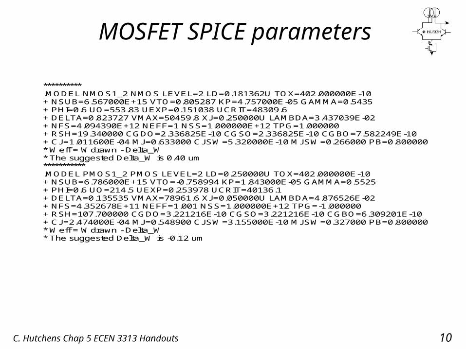
MOSFET SPICE parameters
**********.MODEL NMOS1_2 NMOS LEVEL=2 LD=0.181362U TOX=402.000000E-10+ NSUB=6.567000E+15 VTO=0.805287 KP=4.757000E-05 GAMMA=0.5435+ PHI=0.6 UO=553.83 UEXP=0.151038 UCRIT=48309.6+ DELTA=0.823727 VMAX=50459.8 XJ=0.250000U LAMBDA=3.437039E-02+ NFS=4.094390E+12 NEFF=1 NSS=1.000000E+12 TPG=1.000000+ RSH=19.340000 CGDO=2.336825E-10 CGSO=2.336825E-10 CGBO=7.582249E-10+ CJ=1.011600E-04 MJ=0.633000 CJSW=5.320000E-10 MJSW=0.266000 PB=0.800000* Weff = Wdrawn - Delta_W* The suggested Delta_W is 0.40 um***********.MODEL PMOS1_2 PMOS LEVEL=2 LD=0.250000U TOX=402.000000E-10+ NSUB=6.786000E+15 VTO=-0.758994 KP=1.843000E-05 GAMMA=0.5525+ PHI=0.6 UO=214.5 UEXP=0.253978 UCRIT=40136.1+ DELTA=0.135535 VMAX=78961.6 XJ=0.050000U LAMBDA=4.876526E-02+ NFS=4.352678E+11 NEFF=1.001 NSS=1.000000E+12 TPG=-1.000000+ RSH=107.700000 CGDO=3.221216E-10 CGSO=3.221216E-10 CGBO=6.309201E-10+ CJ=2.474000E-04 MJ=0.548900 CJSW=3.155000E-10 MJSW=0.327000 PB=0.800000* Weff = Wdrawn - Delta_W* The suggested Delta_W is -0.12 um
C. Hutchens Chap 5 ECEN 3313 Handouts 11
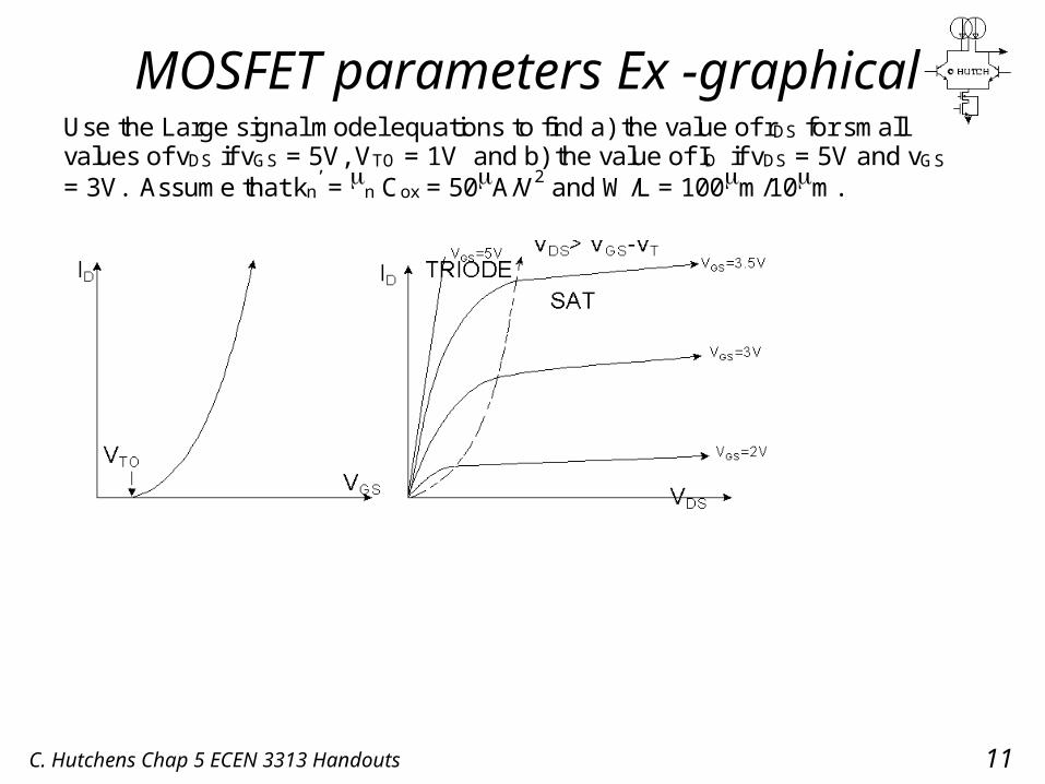
MOSFET parameters Ex -graphicalUse the Large signal model equations to find a) the value of rDS for smallvalues of vDS if vGS = 5V, VTO = 1V and b) the value of ID if vDS = 5V and vGS
= 3V. Assume that kn’ = n Cox = 50A/V2 and W/L = 100m/10m.
C. Hutchens Chap 5 ECEN 3313 Handouts 12
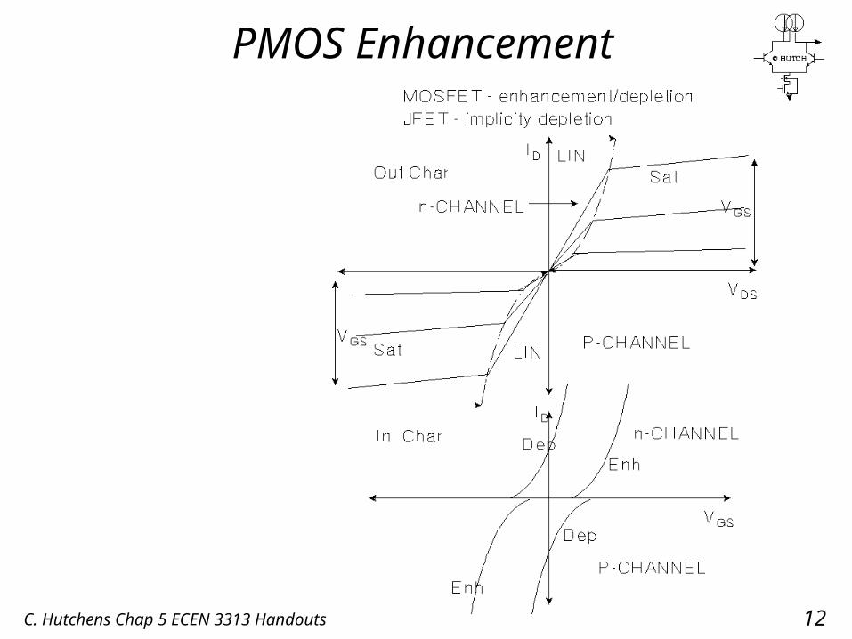
PMOS Enhancement
C. Hutchens Chap 5 ECEN 3313 Handouts 13
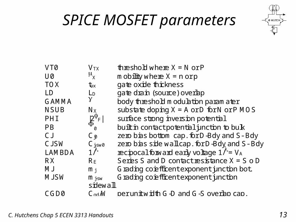
SPICE MOSFET parameters
VT0 VTX threshold where X = N or PU0
X mobility where X = n or pTOX tox gate oxide thicknessLD LD gate drain (source) overlapGAMMA body threshold modulation paramaterNSUB NX substate doping X = A or D for N or P MOSPHI |2F| surface strong inversion potentialPB
0 built in contact potential junction to bulkCJ Cj0 zero bias bottom cap. for D-Bdy and S- BdyCJSW Cj-sw0 zero bias side wall cap. for D-Bdy and S- BdyLAMBDA 1/ recipocal forward early voltage 1/= VA
RX RE Series S and D contact resistance X = S o DMJ mj Grading coiefficent exponent junction bot.MJSW mj-sw Grading coiefficent exponent junction
sidewallCGD0 Cgd/W per unit width G-D and G-S overlap cap.
C. Hutchens Chap 5 ECEN 3313 Handouts 14
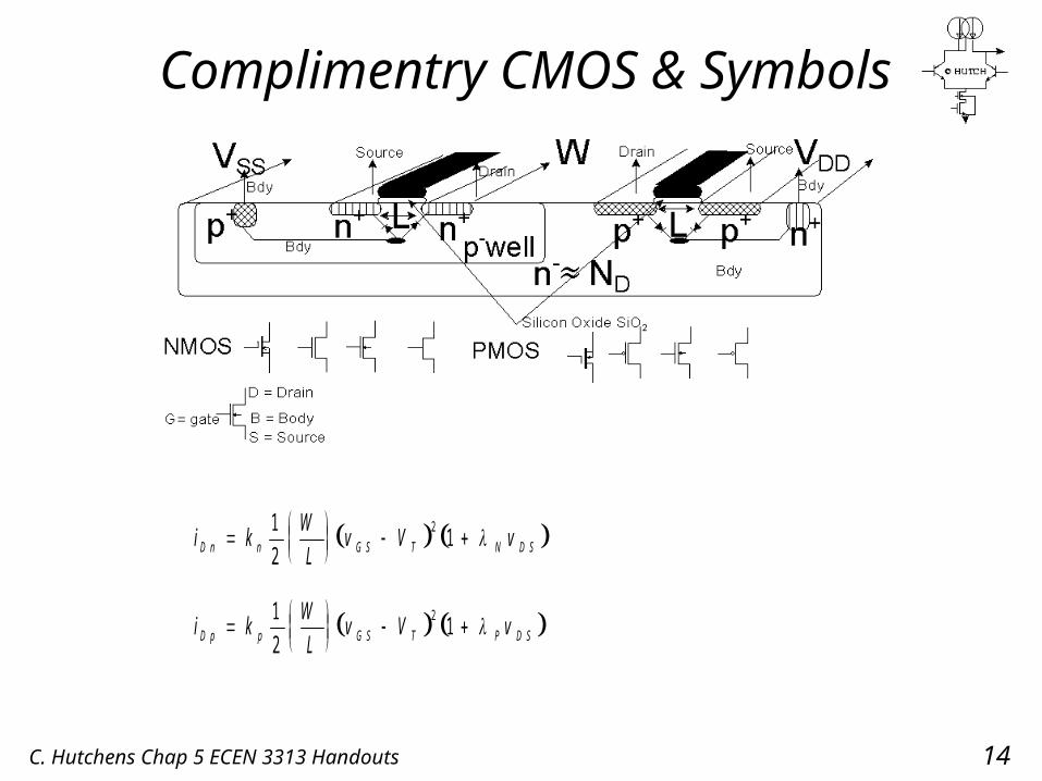
Complimentry CMOS & Symbols
i kW
Lv V vD n n G S T N D S
1
21
2
i kW
Lv V vD p p G S T P D S
1
21
2
C. Hutchens Chap 5 ECEN 3313 Handouts 15
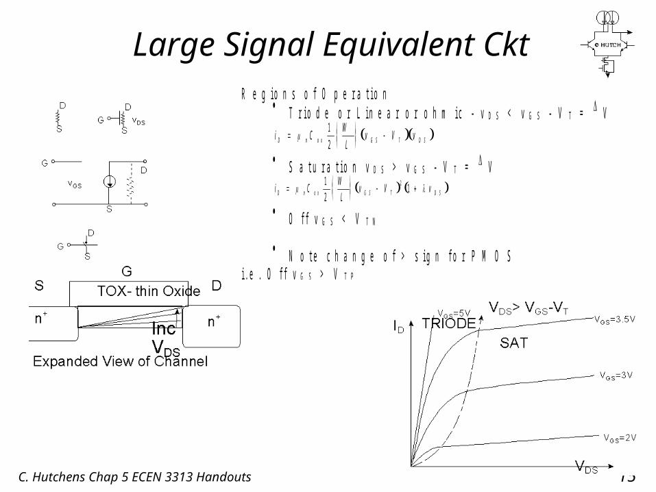
Large Signal Equivalent CktR e g i o n s o f O p e r a t i o n
T r i o d e o r L i n e a r o r o h m i c - v D S < v G S - V T = V
i CW
Lv V vD n o x G S T D S
1
2 S a t u r a t i o n v D S > v G S - V T = V
i CW
Lv V vD n o x G S T D S
1
21
2
O f f v G S < V T N
N o t e c h a n g e o f > s i g n f o r P M O Si . e . O f f v G S > V T P
C. Hutchens Chap 5 ECEN 3313 Handouts 16
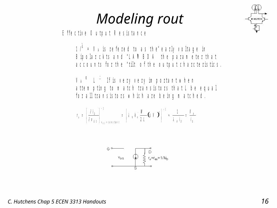
Modeling routE f f e c t i v e O u t p u t R e s i s t a n c e
1 / = V A i s r e f e r e d t o a s t h e e a r l y v o l t a g e i nB i p o l a r c k t s a n d “ L A M B D A ” t h e p a r a m e t e r t h a ta c c o u n t s f o r t h e “ t i l t ” o f t h e o u t p u t c h a r c t e r i s t i c s .
V A L I f i s v e r y v e r y i m p o r t a n t w h e na t t e m p t i n g t o m a t c h t r a n s i s t o r s t h a t L b e e q u a lf o r a l l t r a n s i s t o r s w h i c h a r e b e i n g m a t c h e d .
ri
vk
W
LV
i
V
iuD
G S v c o n s t
N nN D
A
DG S
t a n
'
12
1
2
1
C. Hutchens Chap 5 ECEN 3313 Handouts 17
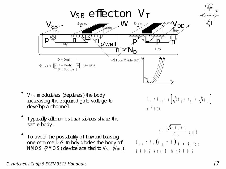
VSB modulates (depletes) the bodyincreasing the required gate voltage todevelop a channel.
Typically all or most transistors share the
same body.To avoid the possibility of forward biasing
one or more D/S to bdy diodes the body ofNMOS (PMOS) device are tied to VSS (VDD).
vSB effect on VT
V V vT T f S B f 0 2 2
w h e r e
2 q N
CX S i
o x a n d
V V vT T S B0 0 X = A f o rN M O S a n d D f o r P M O S
C. Hutchens Chap 5 ECEN 3313 Handouts 18
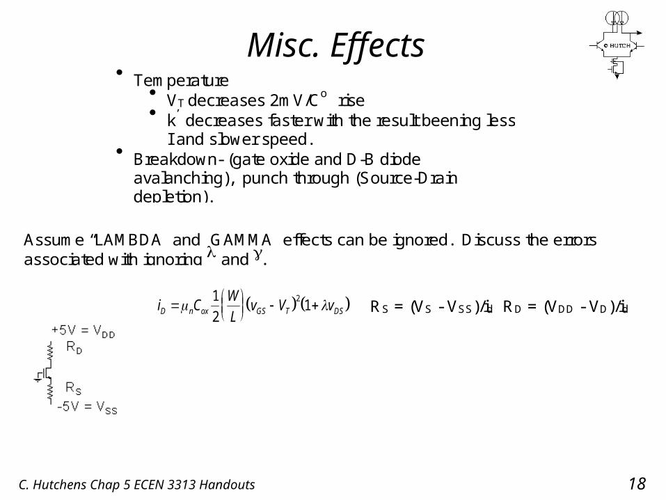
Misc. EffectsTemperature
VT decreases 2mV/Co risek’ decreases faster with the result beening less
I and slower speed.Breakdown- (gate oxide and D-B diode
avalanching), punch through (Source-Draindepletion).
Assume “LAMBDA” and ”GAMMA” effects can be ignored. Discuss the errorsassociated with ignoring and .
i CW
Lv V vD n ox GS T DS
1
21
2 RS = (VS - VSS)/id RD = (VDD - VD)/id
C. Hutchens Chap 5 ECEN 3313 Handouts 19
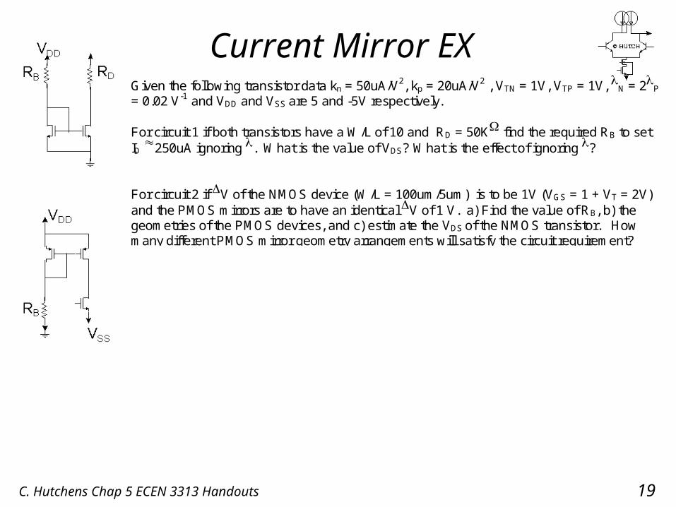
Current Mirror EXGiven the following transistor data kn = 50uA/V2, kp = 20uA/V2 , VTN = 1V, VTP = 1V, N = 2P
= 0.02 V-1 and VDD and VSS are 5 and -5V respectively.
For circuit 1 if both transistors have a W/L of 10 and RD = 50K find the required RB to setID 250uA ignoring . What is the value of VDS? What is the effect of ignoring ?
For circuit 2 if V of the NMOS device (W/L = 100um/5um) is to be 1V (VGS = 1 + VT = 2V)and the PMOS mirrors are to have an identical V of 1 V. a) Find the value of RB, b) thegeometries of the PMOS devices, and c) estimate the VDS of the NMOS transistor. Howmany different PMOS mirror geometry arrangements will satisfy the circuit requirement?
C. Hutchens Chap 5 ECEN 3313 Handouts 20
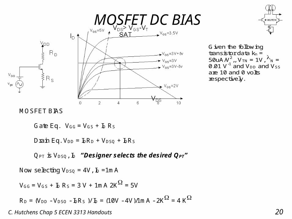
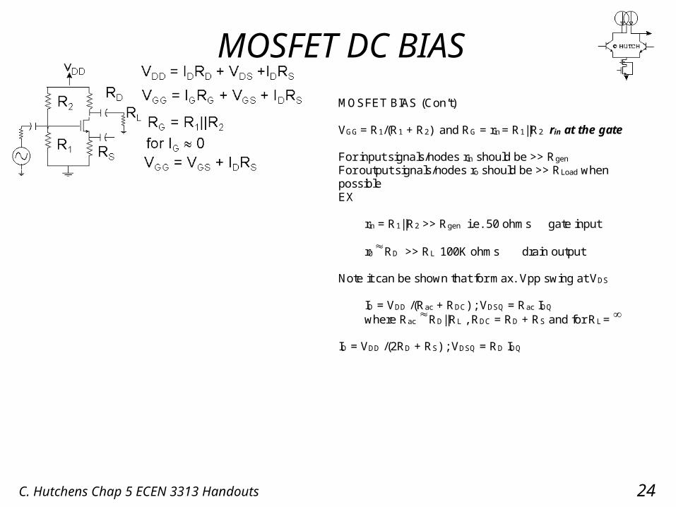
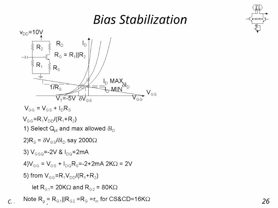
MOSFET DC BIAS
Given the followingtransistor data kn =50uA/V2,, VTN = 1V, N =0.01 V-1 and VDD and VSS
are 10 and 0 voltsrespectively.
MOSFET BIAS
Gate Eq. VGG = VGS + ID RS
Drain Eq. VDD = IDRD + VDSQ + IDRS
QPT is VDSQ, ID “Designer selects the desired QPT”
Now selecting VDSQ = 4V, ID =1mA
VGG = VGS + ID RS = 3 V + 1mA 2K = 5V
RD = (VDD - VDSQ - IDRS )/ ID = (10V - 4V)/1mA - 2K = 4 K
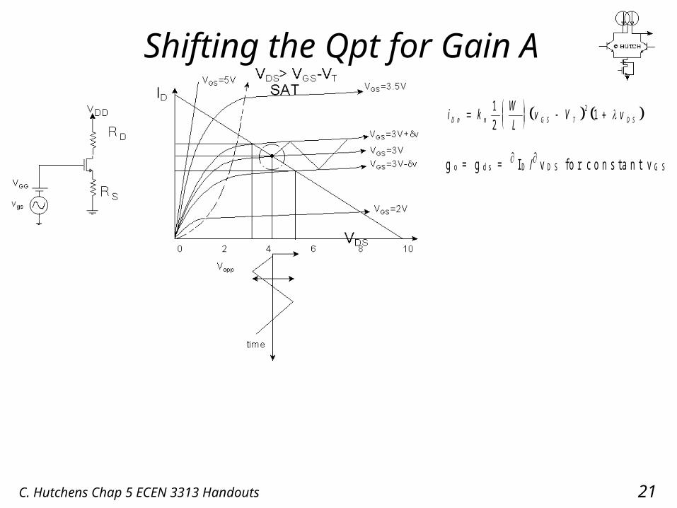
C. Hutchens Chap 5 ECEN 3313 Handouts 21
Shifting the Qpt for Gain A
i kW
Lv V vD n n G S T D S
1
21
2
g o = g d s = I D / v D S f o r c o n s t a n t v G S
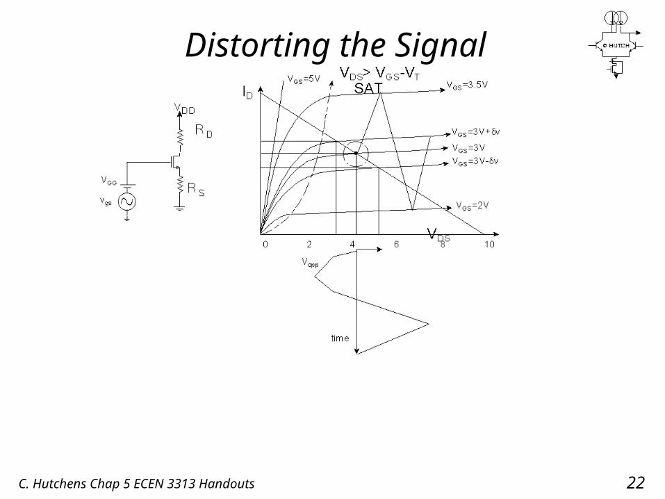
C. Hutchens Chap 5 ECEN 3313 Handouts 22
Distorting the Signal
C. Hutchens Chap 5 ECEN 3313 Handouts 23
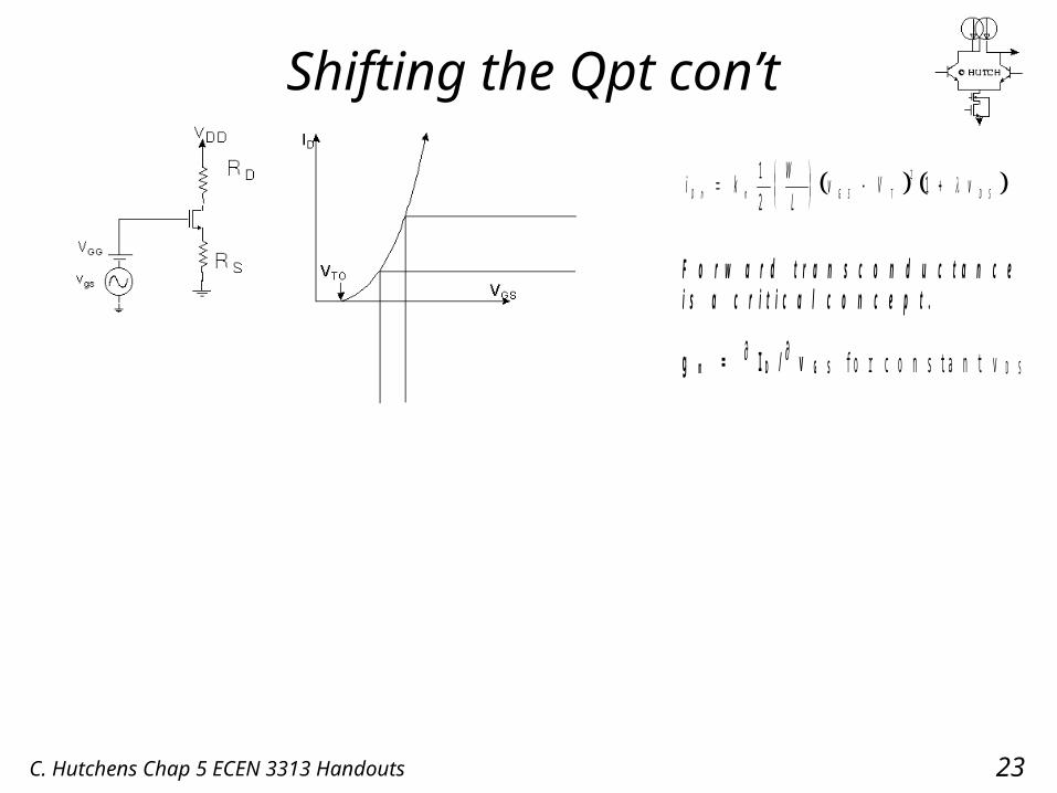
Shifting the Qpt con’t
i kW
Lv V vD n n G S T D S
1
21
2
F o r w a r d t r a n s c o n d u c t a n c ei s a c r i t i c a l c o n c e p t .
g m = I D / v G S f o r c o n s t a n t v D S
C. Hutchens Chap 5 ECEN 3313 Handouts 24
MOSFET DC BIASMOSFET BIAS (Con’t)
VGG = R1/(R1 + R2) and RG = rin = R1||R2 rin at the gate
For input signals/nodes rin should be >> Rgen
For output signals/nodes ro should be >> RLoad whenpossibleEX
rin = R1||R2 >> Rgen i.e. 50 ohms gate input
r0 RD >> RL 100K ohms drain output
Note it can be shown that for max. Vpp swing at VDS
ID = VDD /(Rac + RDC) ; VDSQ = Rac IDQ
where Rac RD||RL , RDC = RD + RS and for RL =
ID = VDD /(2RD + RS) ; VDSQ = RD IDQ
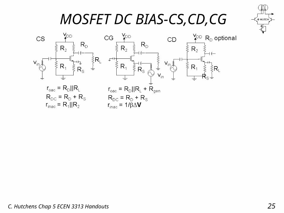
C. Hutchens Chap 5 ECEN 3313 Handouts 25
MOSFET DC BIAS-CS,CD,CG
C. Hutchens Chap 5 ECEN 3313 Handouts 26
Bias Stabilization
C. Hutchens Chap 5 ECEN 3313 Handouts 27
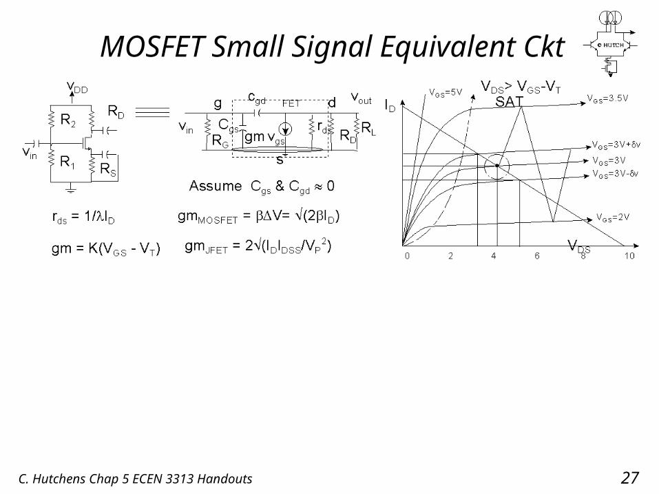
MOSFET Small Signal Equivalent Ckt
C. Hutchens Chap 5 ECEN 3313 Handouts 28
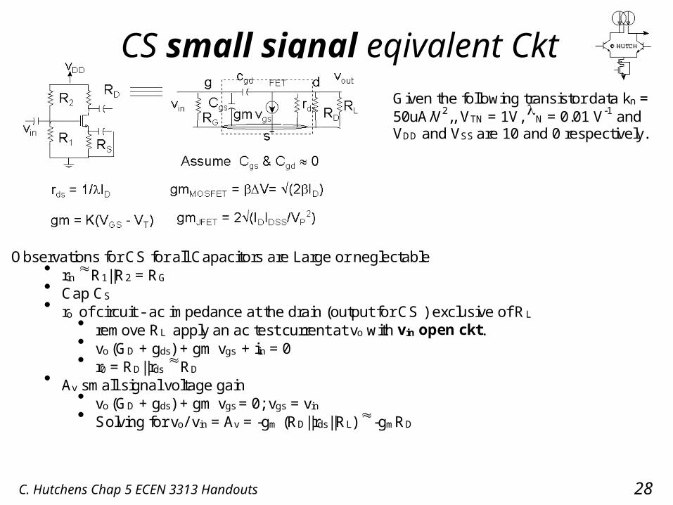
CS small signal eqivalent CktGiven the following transistor data kn =50uA/V2,, VTN = 1V, N = 0.01 V-1 andVDD and VSS are 10 and 0 respectively.
Observations for CS for all Capacitors are Large or neglectable rin R1||R2 = RG Cap CS ro of circuit - ac impedance at the drain (output for CS ) exclusive of RL
remove RL apply an ac test current at vo with vin open ckt. vo (GD + gds) + gm vgs + iin = 0 r0 = RD||rds RD
Av small signal voltage gain vo (GD + gds) + gm vgs = 0; vgs = vin Solving for vo/ vin = Av = -gm (RD||rds||RL) -gmRD
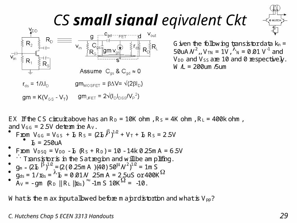
C. Hutchens Chap 5 ECEN 3313 Handouts 29
EX If the CS circuit above has an RD = 10K ohm, RS = 4K ohm, RL = 400k ohm,and VGG = 2.5V determine AV.From VGG = VGS + ID RS = (2ID/)1/2 + VT + ID RS = 2.5V
ID = 250uAFrom VDSQ = VDD - ID (RS + RD) = 10 - 14k 0.25mA = 6.5V Transistor is in the Sat region and will be amplifing.gm = (2ID )1/2 =(2( 0.25mA )(40) 50/V2)1/2 = 1mSgds = 1/ rds = ID = 0.01/V .25mA = 2.5uS or 400KAV = - gm (RD || RL ||rds) -1mS 10K = -10.
What is the max input allowed before major distortion and what is Vpp?
CS small signal eqivalent CktGiven the following transistor data kn =50uA/V2,, VTN = 1V, N = 0.01 V-1 andVDD and VSS are 10 and 0 respectively.W/L = 200um/5um

C. Hutchens Chap 5 ECEN 3313 Handouts 30
EX If the CS circuit above has an RD = 10K ohm, RS = 4K ohm, RL = 400k ohm,and VGG = 2.5V determine AV.From VGG = VGS + ID RS = (2ID/)1/2 + VT + ID RS = 2.5V
ID = 250uAFrom VDSQ = VDD - ID (RS + RD) = 10 - 14k 0.25mA = 6.5V Transistor is in the Sat region and will be amplifing.gm = (2ID )1/2 =(2( 0.25mA )(40) 50/V2)1/2 = 1mSgds = 1/ rds = ID = 0.01/V .25mA = 2.5uS or 400KAV = - gm (RD || RL ||rds) -1mS 10K = -10.
What is the max input allowed before major distortion and what is Vpp?
CS small signal eqivalent CktGiven the following transistor data kn =50uA/V2,, VTN = 1V, N = 0.01 V-1 andVDD and VSS are 10 and 0 respectively.W/L = 200um/5um
C. Hutchens Chap 5 ECEN 3313 Handouts 31
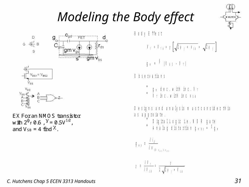
Modeling the Body effectB o d y E f f e c t
V V vT T f S B f 0 2 2
g m = ( V G S - V T )
O b s e r v a t i o n s
g m d e c . w i t h i n c . V T V T i n c . w i t h i n c v S B
D e s i g n s a n d a n a l y s i s m u s t c o n s i d e r t h i sa s a p p r o i a t e .
D i g i t a l L o g i c i . e . N O R g a t e A n a l o g d i s t o r t i o n g m b c = g m
gi
vm bD
s b v vG S D S
V
V VT
S B f S B2 2
EX For an NMOS transistorwith 2f 0.6 , = 0.5V1/2,and VSB = 4 find .
C. Hutchens Chap 5 ECEN 3313 Handouts 32
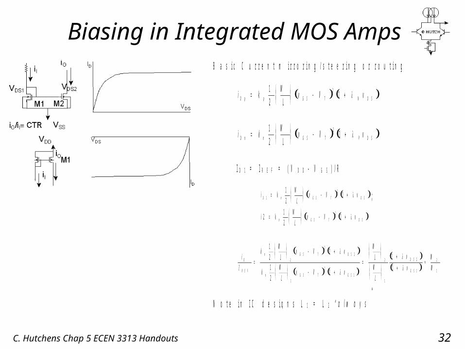
Biasing in Integrated MOS AmpsB a s i c C u r r e n t m i r r o r i n g / s t e e r i n g o r r o u t i n g
i kW
Lv V vD p p G S T N D S
1
21
2
i kW
Lv V vD n n G S T P D S
1
21
2
I D 1 = I R E F = ( V D D - V G S ) / R
i kW
Lv V vD n G S T D S1
21
21
;
i kW
Lv V vn G S T D S2
1
21
2
i
I
kW
Lv V v
kW
Lv V v
W
LW
L
v
v
W
WO
R E F
n G S T D S
n G S T G S
D S
G S
1
21
1
21
1
12
2
2
1
2
1
2
1
2
1
2
1
N o t e i n I C d e s i g n s L 1 = L 2 “ a l w a y s ”
C. Hutchens Chap 5 ECEN 3313 Handouts 33
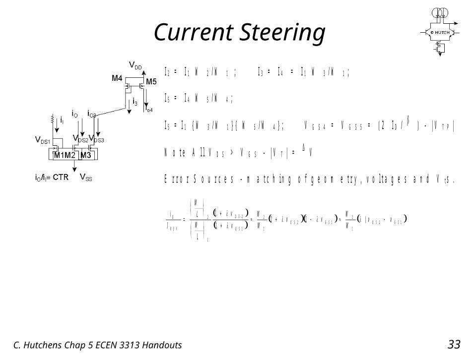
Current SteeringI 2 = I 1 W 2 / W 1 ; I 3 = I 4 = I 1 W 3 / W 1 ;
I 5 = I 4 W 5 / W 4 ;
I 5 = I 1 { W 3 / W 1 } { W 5 / W 4 } ; V G S 4 = V G S 5 = ( 2 I D / ) - | V T P |
N o t e A l l V D S > V G S - | V T | = V
E r r o r S o u r c e s - m a t c h i n g o f g e o m e t r y , v o l t a g e s a n d V t s .
i
I
W
LW
L
v
v
W
Wv v
W
Wv vO
R E F
D S
G SD S G S D S G S
2
1
2
1
2
12 1
2
12 1
1
11 1
(
C. Hutchens Chap 5 ECEN 3313 Handouts 34
IC Biasing of the Basic MOS amps
C. Hutchens Chap 5 ECEN 3313 Handouts 35
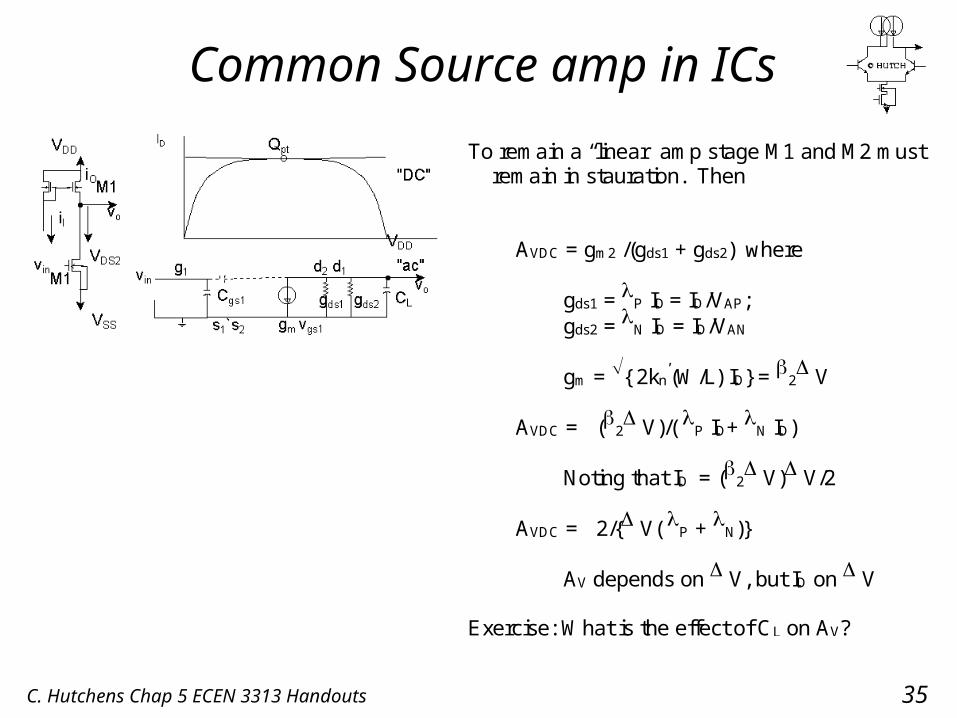
Common Source amp in ICs
To remain a “linear” amp stage M1 and M2 mustremain in stauration. Then
AVDC = gm2 /(gds1 + gds2) where
gds1 = P ID = ID/VAP; gds2 = N ID = ID/VAN
gm = { 2kn’(W/L) ID} = 2
V
AVDC = (2 V)/( P ID+ N ID)
Noting that ID = (2 V) V/2
AVDC = 2/{ V( P + N)}
AV depends on V, but ID on V
Exercise: What is the effect of CL on AV?
C. Hutchens Chap 5 ECEN 3313 Handouts 36
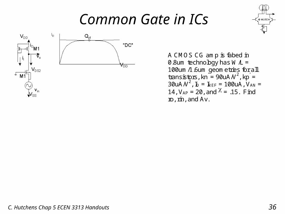
Common Gate in ICs
A CMOS CG amp is fabed in0.8um technology has W/L =100um/1.6um geometries for alltransistors, kn’ = 90uA/V2, kp’ =30uA/V2, ID = IREF = 100uA, VAN =14, VAP = 20, and = .15. Findro, rin, and Av.
C. Hutchens Chap 5 ECEN 3313 Handouts 37
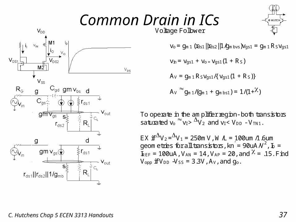
Common Drain in ICsVoltage Follower
vo = gm1 (rds1||rds2||1/gmbvs)vgs1 = gm1 RSvgs1
vin = vgs1 + vo = vgs1(1 + RS)
AV = gm1 RSvgs1/{ vgs1(1 + RS)}
AV gm1/(gm1 + gmbs1) = 1/(1+)
To operate in the amplifier region- both transistorssaturated vo vI > V2 and vI < VDD - VTN1.
EX if V2 =V1 = 250mV, W/L = 100um/1.6umgeometries for all transistors, kn’ = 90uA/V2, ID =IREF = 100uA, VAN = 14, VAP = 20, and = .15. FindVopp if VDD -VSS = 3.3V, AV, and go.
C. Hutchens Chap 5 ECEN 3313 Handouts 38
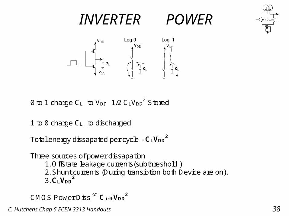
INVERTER POWER
0 to 1 charge CL to VDD 1/2 CLVDD2 Stored
1 to 0 charge CL to discharged
Total energy dissapated per cycle - CLVDD2
Three sources of power dissapation1. Offstate leakage currents(subthreshold )2. Shunt currents (During transiotion both Device are on).3. CLVDD
2
CMOS Power Diss Cleff VDD2
C. Hutchens Chap 5 ECEN 3313 Handouts 39
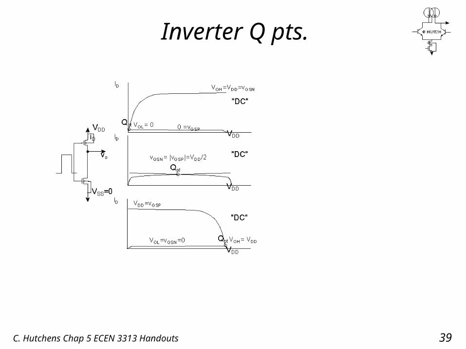
Inverter Q pts.
C. Hutchens Chap 5 ECEN 3313 Handouts 40
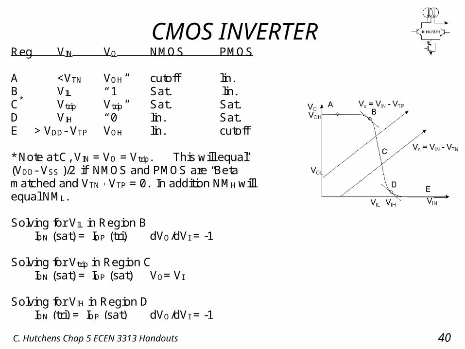
CMOS INVERTERReg VIN VO NMOS PMOS
A <VTN VOH cutoff lin.B VIL “ 1” Sat. lin.C* Vtrip Vtrip Sat. Sat.D VIH “ 0” lin. Sat.E > VDD- VTP VOH lin. cutoff
* Note at C, VIN = VO = Vtrip. This will equal(VDD- VSS )/2 if NMOS and PMOS are “Beta”matched and VTN + VTP = 0. In addition NMH willequal NML.
Solving for VIL in Region BIDN (sat) = IDP (tri) dVO/dVI = -1
Solving for Vtrip in Region CIDN (sat) = IDP (sat) VO= VI
Solving for VIH in Region DIDN (tri) = IDP (sat) dVO/dVI = -1
C. Hutchens Chap 5 ECEN 3313 Handouts 41
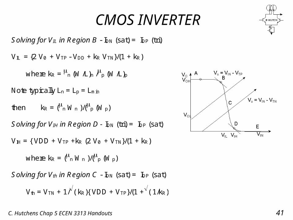
CMOS INVERTERSolving for VIL in Region B - IDN (sat) = IDP (tri)
VIL = {2 V0 + VTP - VDD + kR VTN}/(1 + kR)
where kR = n (W/L)n /p (W/L)p
Note typically Ln = Lp = Lmin
then kR = (n Wn )/(p (Wp)
Solving for VIH in Region D - IDN (tri) = IDP (sat)
VIH = { VDD + VTP +kR (2 V0 + VTN}/(1 + kR)
where kR = (n Wn )/(p (Wp)
Solving for Vth in Region C - IDN (sat) = IDP (sat)
Vth = VTN + 1/( kR){ VDD + VTP}/(1 +( 1/kR)
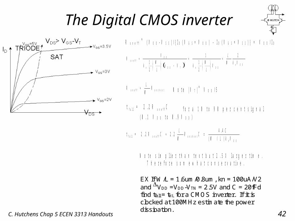
C. Hutchens Chap 5 ECEN 3313 Handouts 42
The Digital CMOS inverterR o n e f f ( V D D - V S S ) / { I D ( V G S = V D D ) - I D ( V G S = V S S ) } = V D D / I D
R o n e f f
V
kW
Lv V k
W
LV
L
W k VD D
n D D T n D Dn D D1
2
11
2
22
R o n e f f L
WR o n s h e e t N o t e | V T | V D D / 5
t = 2 . 2 Rf a l l o n e f f C f o r a 1 0 t o 9 0 p e r c e n t s i g n a l( 0 . 1 V D D t o 0 . 9 V D D )
t = 2 . 2 Rf a l l o n e f f CL
WR C
C
W L k Vo n s h e e tn D D
2 24 4
..
( / )
N o t e s i m p l i e r t h a n t e x t b u t 2 . 5 X l a r g e r t i m e .T h e r e f o r e s o m e w h a t c o n s e r v a t i v e .
EX If W/L = 1.6um/0.8um, kn = 100uA/V2and VDD =VDD-VTN = 2.5V and C = 20fFdfind tfall = tHL for a CMOS inverter. If it isclocked at 100MHz estimate the powerdissipation.
C. Hutchens Chap 5 ECEN 3313 Handouts 43
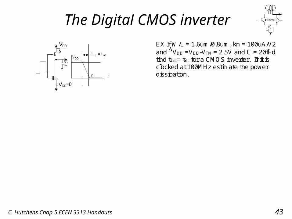
The Digital CMOS inverterEX If W/L = 1.6um/0.8um, kn = 100uA/V2and VDD =VDD-VTN = 2.5V and C = 20fFdfind tfall = tHL for a CMOS inverter. If it isclocked at 100MHz estimate the powerdissipation.
C. Hutchens Chap 5 ECEN 3313 Handouts 44
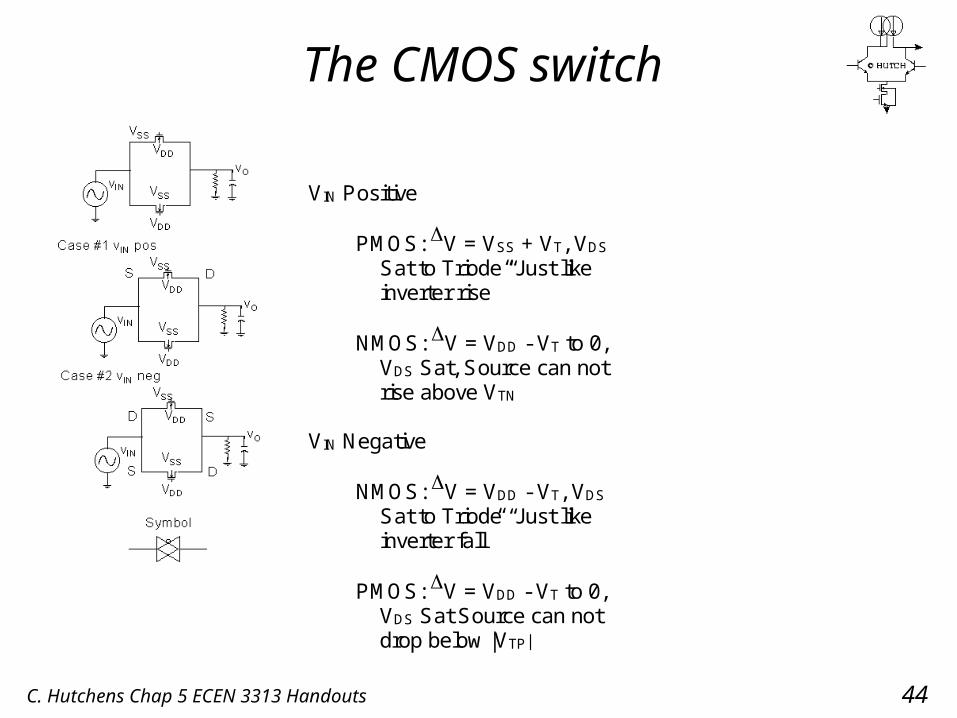
The CMOS switch
VIN Positive
PMOS: V = VSS + VT, VDS
Sat to Triode “Just likeinverter rise”
NMOS: V = VDD - VT to 0,VDS Sat, Source can notrise above VTN
VIN Negative
NMOS: V = VDD - VT, VDS
Sat to Triode “Just likeinverter fall”
PMOS: V = VDD - VT to 0,VDS Sat Source can notdrop below |VTP|
C. Hutchens Chap 5 ECEN 3313 Handouts 45
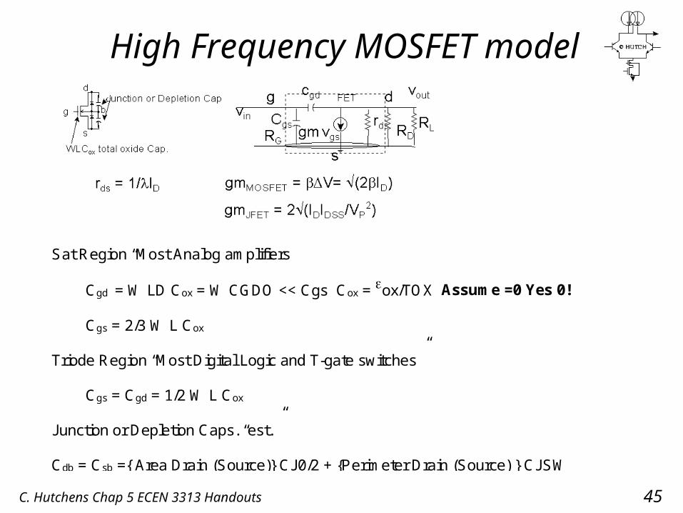
High Frequency MOSFET model
Sat Region “Most Analog amplifiers”
Cgd = W LD Cox = W CGDO << Cgs Cox = ox/TOX Assume =0 Yes 0!
Cgs = 2/3 W L Cox
Triode Region “Most Digital Logic and T-gate switches”
Cgs = Cgd = 1/2 W L Cox
Junction or Depletion Caps. “est.”
Cdb = Csb ={ Area Drain (Source)} CJ0/2 + {Perimeter Drain (Source) } CJSW
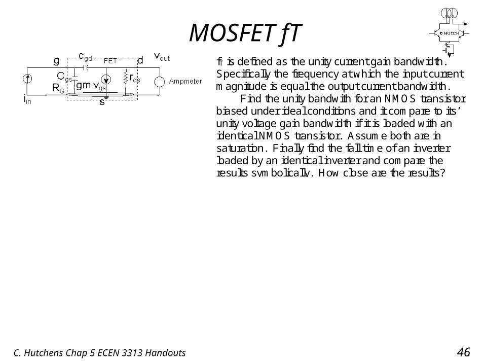
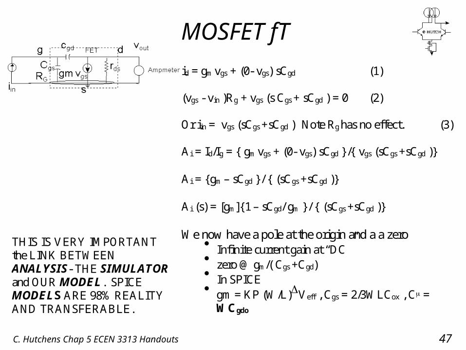
C. Hutchens Chap 5 ECEN 3313 Handouts 46
MOSFET fTfT is defined as the unity current gain bandwidth.Specifically the frequency at which the input currentmagnitude is equal the output current bandwidth.
Find the unity bandwith for an NMOS transistorbiased under ideal conditions and it compare to its’unity voltage gain bandwidth if it is loaded with anidentical NMOS transistor. Assume both are insaturation. Finally find the fall time of an inverterloaded by an identical inverter and compare theresults symbolically. How close are the results?
C. Hutchens Chap 5 ECEN 3313 Handouts 47
MOSFET fT
id = gm vgs + (0- vgs) sCgd (1)
(vgs - vin )Rg + vgs (s Cgs + sCgd ) = 0 (2)
Or iin = vgs (sCgs +sCgd ) Note Rg has no effect. (3)
Ai = Id/Ig = { gm vgs + (0- vgs) sCgd }/{ vgs (sCgs +sCgd )}
Ai = {gm – sCgd }/ { (sCgs +sCgd )}
Ai (s) = [gm]{1 – sCgd/ gm }/ { (sCgs +sCgd )}
We now have a pole at the origin and a a zero Infinite current gain at “DC” zero @ gm/( Cgs +Cgd) In SPICE gm = KP (W/L)Veff , Cgs = 2/3WLCox , C =
WCgdo
THIS IS VERY IMPORTANTthe LINK BETWEENANALYSIS- THE SIMULATORand OUR MODEL. SPICEMODELS ARE 98% REALITYAND TRANSFERABLE.
C. Hutchens Chap 5 ECEN 3313 Handouts 48
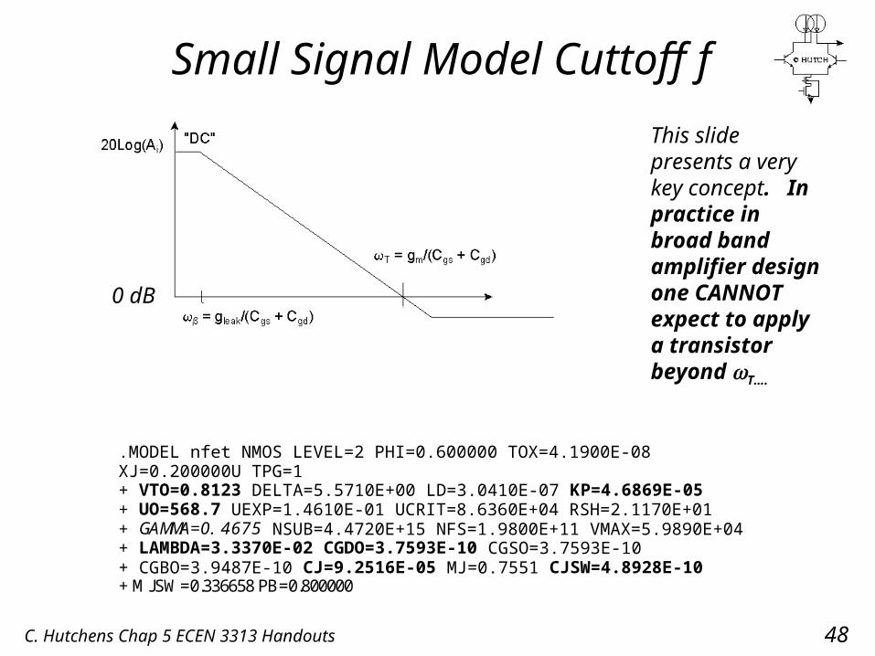
Small Signal Model Cuttoff f
This slide presents a very key concept. In practice in broad band amplifier design one CANNOT expect to apply a transistor beyond T….
.MODEL nfet NMOS LEVEL=2 PHI=0.600000 TOX=4.1900E-08XJ=0.200000U TPG=1+ VTO=0.8123 DELTA=5.5710E+00 LD=3.0410E-07 KP=4.6869E-05+ UO=568.7 UEXP=1.4610E-01 UCRIT=8.6360E+04 RSH=2.1170E+01+ GAMMA=0.4675 NSUB=4.4720E+15 NFS=1.9800E+11 VMAX=5.9890E+04+ LAMBDA=3.3370E-02 CGDO=3.7593E-10 CGSO=3.7593E-10+ CGBO=3.9487E-10 CJ=9.2516E-05 MJ=0.7551 CJSW=4.8928E-10+ MJSW=0.336658 PB=0.800000
0 dB
C. Hutchens Chap 5 ECEN 3313 Handouts 49
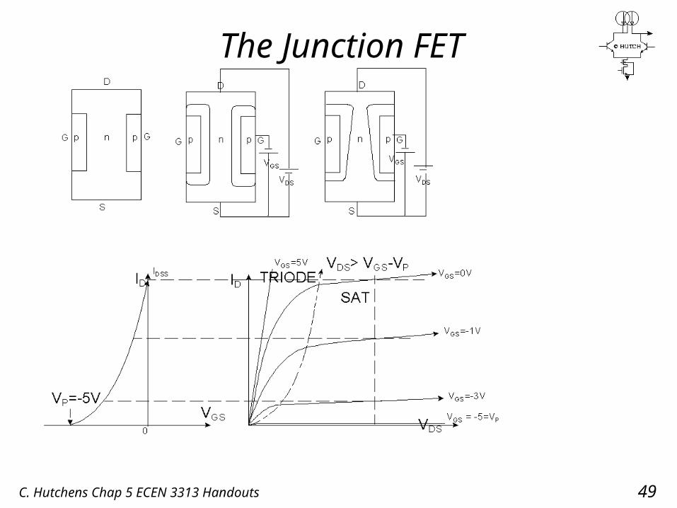
The Junction FET
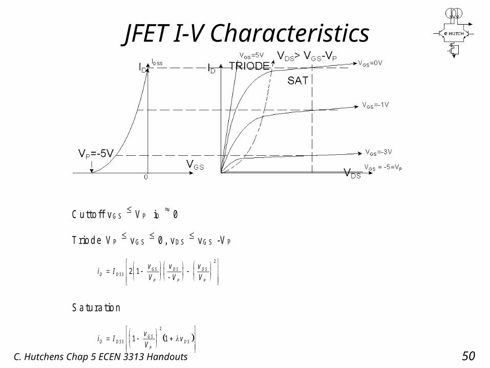
C. Hutchens Chap 5 ECEN 3313 Handouts 50
JFET I-V Characteristics
C u t to f f v G S V P iD 0
T r io d e V P v G S 0 , v D S v G S - V P
i Iv
V
v
V
v
VD D S SG S
P
D S
P
D S
P
2 12
S a tu r a t io n
i Iv
VvD D S S
G S
PD S
1 12
C. Hutchens Chap 5 ECEN 3313 Handouts 51
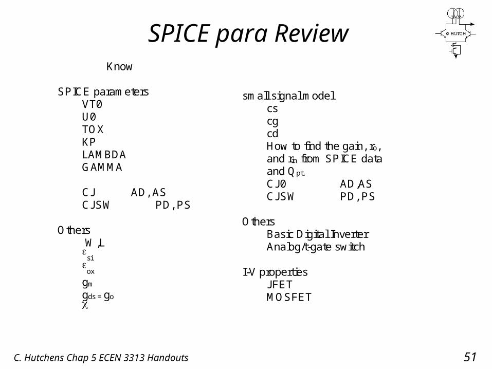
SPICE para ReviewKnow
SPICE parametersVT0U0TOXKPLAMBDAGAMMA
CJ AD, ASCJSW PD, PS
Others W,L
si
ox
gm gds = go
small signal modelcscgcdHow to find the gain, ro,and rin from SPICE dataand Qpt.
CJ0 AD,ASCJSW PD, PS
OthersBasic Digital InverterAnalog/t-gate switch
I-V propertiesJFETMOSFET


