Prepared by: Prof. Ajaykumar T. Shah Blog: aforajayshahnirma.wordpress.com.
ENABLING INTERPOSER-BASED DISINTEGRATION OF MULTI-CORE PROCESSORS
by
Ajaykumar Kannan
A thesis submitted in conformity with the requirementsfor the degree of Master of Applied Science
in the The Edward S. Rogers Sr. Department of Electrical & Computer EngineeringUniversity of Toronto
c© Copyright 2015 by Ajaykumar Kannan

Abstract
Enabling Interposer-based Disintegration of Multi-core Processors
Ajaykumar KannanMaster of Applied Science
The Edward S. Rogers Sr. Department of Electrical & Computer EngineeringUniversity of Toronto
2015
Silicon interposers enable high-performance processors to integrate a significant amount of in-package
memory, thereby providing huge bandwidth gains while reducing the costs of accessing memory. Once
the price has been paid for the interposer, there are new opportunities to exploit it and provide other
system benefits. We consider how the routing resources afforded by the interposer can be used to im-
prove the network-on-chip’s (NoC) capabilities and use the interposer to “disintegrate” a multi-core
chip into smaller chips that individually and collectively cost less to manufacture than a large mono-
lithic chip. However, distributing a system across many pieces of silicon causes the overall NoC to
become fragmented, thereby decreasing performance as core-to-core communications between differ-
ent chips must now be routed through the interposer. We study the performance-cost trade-offs of
implementing an interposer-based, multi-chip, multi-core system and propose new interposer NoC
organizations to mitigate the performance challenges while preserving the cost benefits.
ii

Acknowledgements
First, I would like to express my sincerest gratitude to my supervisor, Natalie Enright Jerger, for herguidance and motivation during my time here. I have learned a lot from her expertise in computerarchitecture, on-chip networks, and research methodologies. I have been very lucky in having her asmy mentor and she has been just wonderful to work with.
I would also like to thank Gabriel Loh at AMD Corp., for his numerous inputs, suggestions andguidance throughout the work that I have been a part of during my programme. It has been a greatopportunity and learning experience to have worked with him.
I also extend my thanks to the NEJ research group for all the support, help, and guidance. It hasbeen a privilege to have had the chance to interact and discuss various ideas and subjects with them,technical and otherwise, and get their invaluable feedback. I would also like to thank the graduatestudents in Prof. Andreas Moshovos’ research group for the help during those crucial times, and theirfeedback on our work.
I would like to thank my committee- professors Andreas Moshovos, Jason Anderson, and JoshTaylor for their insights and feedback on our work.
I would like to thank my friends and family who have helped me along the way, knowingly orunknowingly. Finally, I would like to thank my parents who started me on this path a long time agoand helped me get to this point in my life. I would not be here without them.
iii
Contents
1 Introduction 11.1 Research Highlights . . . . . . . . . . . . . . . . . . . . . . . . . . . . . . . . . . . . . . . . . 21.2 Organization . . . . . . . . . . . . . . . . . . . . . . . . . . . . . . . . . . . . . . . . . . . . . 2
2 Background 32.1 Network on Chip . . . . . . . . . . . . . . . . . . . . . . . . . . . . . . . . . . . . . . . . . . 4
2.1.1 Network Parameters and Metrics . . . . . . . . . . . . . . . . . . . . . . . . . . . . . 42.1.2 Network Topology . . . . . . . . . . . . . . . . . . . . . . . . . . . . . . . . . . . . . 5
2.2 Die-Stacking . . . . . . . . . . . . . . . . . . . . . . . . . . . . . . . . . . . . . . . . . . . . . 62.2.1 2.5D vs. 3D Stacking . . . . . . . . . . . . . . . . . . . . . . . . . . . . . . . . . . . . 7
2.3 Silicon Interposers and Their Networks . . . . . . . . . . . . . . . . . . . . . . . . . . . . . 8
3 Motivation 93.1 Chip Disintegration . . . . . . . . . . . . . . . . . . . . . . . . . . . . . . . . . . . . . . . . . 9
3.1.1 Chip Cost Analysis . . . . . . . . . . . . . . . . . . . . . . . . . . . . . . . . . . . . . 103.2 Integration of smaller chips . . . . . . . . . . . . . . . . . . . . . . . . . . . . . . . . . . . . 12
3.2.1 Silicon Interposer-Based Chip Integration . . . . . . . . . . . . . . . . . . . . . . . . 133.2.2 Limitations of Cost Analysis . . . . . . . . . . . . . . . . . . . . . . . . . . . . . . . 15
3.3 The Research Problem . . . . . . . . . . . . . . . . . . . . . . . . . . . . . . . . . . . . . . . 15
4 NoC Architecture 174.1 Baseline Architecture . . . . . . . . . . . . . . . . . . . . . . . . . . . . . . . . . . . . . . . . 174.2 Routing Protocol . . . . . . . . . . . . . . . . . . . . . . . . . . . . . . . . . . . . . . . . . . 174.3 Network Topology . . . . . . . . . . . . . . . . . . . . . . . . . . . . . . . . . . . . . . . . . 19
4.3.1 Misaligned Topologies . . . . . . . . . . . . . . . . . . . . . . . . . . . . . . . . . . . 204.3.2 The ButterDonut Topology . . . . . . . . . . . . . . . . . . . . . . . . . . . . . . . . 224.3.3 Comparing Topologies . . . . . . . . . . . . . . . . . . . . . . . . . . . . . . . . . . . 234.3.4 Deadlock Freedom . . . . . . . . . . . . . . . . . . . . . . . . . . . . . . . . . . . . . 24
4.4 Physical implementation . . . . . . . . . . . . . . . . . . . . . . . . . . . . . . . . . . . . . . 244.4.1 µbump Overheads . . . . . . . . . . . . . . . . . . . . . . . . . . . . . . . . . . . . . 25
5 Methodology and Evaluation 275.1 Methodology . . . . . . . . . . . . . . . . . . . . . . . . . . . . . . . . . . . . . . . . . . . . 27
5.1.1 Synthetic Workloads . . . . . . . . . . . . . . . . . . . . . . . . . . . . . . . . . . . . 275.1.2 SynFull Simulations . . . . . . . . . . . . . . . . . . . . . . . . . . . . . . . . . . . . 285.1.3 Full-System Simulations . . . . . . . . . . . . . . . . . . . . . . . . . . . . . . . . . . 29
5.2 Experimental Evaluation . . . . . . . . . . . . . . . . . . . . . . . . . . . . . . . . . . . . . . 305.2.1 Performance . . . . . . . . . . . . . . . . . . . . . . . . . . . . . . . . . . . . . . . . . 305.2.2 Load vs. Latency Analysis . . . . . . . . . . . . . . . . . . . . . . . . . . . . . . . . . 335.2.3 Routing Protocols . . . . . . . . . . . . . . . . . . . . . . . . . . . . . . . . . . . . . . 355.2.4 Power and Area Modelling . . . . . . . . . . . . . . . . . . . . . . . . . . . . . . . . 355.2.5 Combining Cost and Performance . . . . . . . . . . . . . . . . . . . . . . . . . . . . 375.2.6 Clocking Across Chips . . . . . . . . . . . . . . . . . . . . . . . . . . . . . . . . . . . 38
iv

5.2.7 Non-disintegrated Interposer NoCs . . . . . . . . . . . . . . . . . . . . . . . . . . . 39
6 Related Work 41
7 Future Directions & Conclusions 437.1 Future Directions . . . . . . . . . . . . . . . . . . . . . . . . . . . . . . . . . . . . . . . . . . 43
7.1.1 New Chip-design Concerns . . . . . . . . . . . . . . . . . . . . . . . . . . . . . . . . 437.1.2 Software-based Mitigation of Multi-Chip Interposer Effects . . . . . . . . . . . . . 43
7.2 Conclusion . . . . . . . . . . . . . . . . . . . . . . . . . . . . . . . . . . . . . . . . . . . . . . 44
Bibliography 45
v
List of Tables
3.1 Yield Analysis for multi-core chips . . . . . . . . . . . . . . . . . . . . . . . . . . . . . . . . 113.2 Parameters for the chip yield calculations . . . . . . . . . . . . . . . . . . . . . . . . . . . . 143.3 Yield Rates versus Percentage Active-Interposer . . . . . . . . . . . . . . . . . . . . . . . . 14
4.1 Comparison of Interposer NoC Topologies . . . . . . . . . . . . . . . . . . . . . . . . . . . 24
5.1 NoC simulation parameters . . . . . . . . . . . . . . . . . . . . . . . . . . . . . . . . . . . . 285.2 Full-System Configuration . . . . . . . . . . . . . . . . . . . . . . . . . . . . . . . . . . . . . 295.3 PARSEC Benchmark Characteristics . . . . . . . . . . . . . . . . . . . . . . . . . . . . . . . 335.4 Peak Network Operating Frequency . . . . . . . . . . . . . . . . . . . . . . . . . . . . . . . 37
vi

List of Figures
2.1 Conventional NoC . . . . . . . . . . . . . . . . . . . . . . . . . . . . . . . . . . . . . . . . . 52.2 NoC Topologies for 64-node Systems . . . . . . . . . . . . . . . . . . . . . . . . . . . . . . 52.3 Virtex-7 2000T FGPA . . . . . . . . . . . . . . . . . . . . . . . . . . . . . . . . . . . . . . . . 62.4 AMD’s HBM System . . . . . . . . . . . . . . . . . . . . . . . . . . . . . . . . . . . . . . . . 62.5 64-core Interposer System with DRAM Stacks . . . . . . . . . . . . . . . . . . . . . . . . . . 7
3.1 300mm wafers - Chip sizes versus yield . . . . . . . . . . . . . . . . . . . . . . . . . . . . . 103.2 Average number of 64-core SoCs per wafer per 100MHz bin . . . . . . . . . . . . . . . . . 123.3 Comparison of Multi-Socket and MCM RISC Microprocessor Chip Sets . . . . . . . . . . . 133.4 Normalized cost versus Execution Time . . . . . . . . . . . . . . . . . . . . . . . . . . . . . 15
4.1 Proposed 2.5D multi-chip system . . . . . . . . . . . . . . . . . . . . . . . . . . . . . . . . . 184.2 Side-View of Conventional and Proposed Design . . . . . . . . . . . . . . . . . . . . . . . . 194.3 Link utilization for a single horizontal row . . . . . . . . . . . . . . . . . . . . . . . . . . . 204.4 Baseline Topologies for the interposer . . . . . . . . . . . . . . . . . . . . . . . . . . . . . . 214.5 Perspective and side views of concentration and misalignment . . . . . . . . . . . . . . . . 214.6 Misaligned interposer NoC Topologies . . . . . . . . . . . . . . . . . . . . . . . . . . . . . . 224.7 ButterDonut Topologies . . . . . . . . . . . . . . . . . . . . . . . . . . . . . . . . . . . . . . 234.8 Active versus Passive Interposer Implementation . . . . . . . . . . . . . . . . . . . . . . . 25
5.1 Average packet latency for different topologies . . . . . . . . . . . . . . . . . . . . . . . . . 315.2 Average packet latency results - SynFull . . . . . . . . . . . . . . . . . . . . . . . . . . . . . 325.3 Distribution of message latencies . . . . . . . . . . . . . . . . . . . . . . . . . . . . . . . . . 325.4 Normalized Runtime For Full-System Simulations . . . . . . . . . . . . . . . . . . . . . . . 335.5 Latency and Saturation throughput . . . . . . . . . . . . . . . . . . . . . . . . . . . . . . . . 345.6 Latency & Saturation throughput - Separated memory & coherence traffic . . . . . . . . . 355.7 Routing Protocols . . . . . . . . . . . . . . . . . . . . . . . . . . . . . . . . . . . . . . . . . . 365.8 Power and area results in 45nm normalized to mesh . . . . . . . . . . . . . . . . . . . . . . 365.9 Delay-Cost Comparison . . . . . . . . . . . . . . . . . . . . . . . . . . . . . . . . . . . . . . 385.10 Impact of clock crossing latency on average packet latency with 16-core die . . . . . . . . 395.11 Load-latency curves for a monolithic chip . . . . . . . . . . . . . . . . . . . . . . . . . . . . 39
vii
Chapter 1
Introduction
As computers require more and more performance, it becomes imperative to design faster and cheapercomputing platforms. One of the biggest applications of computers today is their use in data-centersand server farms. Here, they are constantly running near peak performance and improving the speedor energy efficiency, even by a small margin, can have a large impact in the long run. Two importantfactors that we would like to mention here are that these high-performance systems typically have alarge number of computing cores (on the same chip, on the same mother-board, or even on differentmachines) and large amounts of memory to cater to user demands. One evolving technology thatmight be able to cater to these growing demands is the use of 3D stacking to fit more computationallogic inside a single chip. This has the advantage of occupying less area but also providing faster accessbetween components (the vertical distance to traverse would be much smaller than crossing the lengthof the chip). However, at the moment, 3D stacking has several obstacles which prevents laying outmultiple chips on top of each other in a 3-dimensional stack, the main one being thermal issues 1. Acheaper and more feasible way of approaching multi-chip integration is using a silicon interposer toconnect each of the components. This approach is known as 2.5D stacking.
A silicon interposer is essentially a large piece of silicon die with transistors and metal layers thatserves as a base for the package. Multiple chips are placed face-down (with the metal layers of thechip facing the metal layers of the interposer) on the interposer. The chip is then connected to theinterposer through micro-bumps (µbumps). The wiring layer on the interposer is used to make chip-to-chip connections. Using an interposer does not prevent the use of 3D stacking. In fact, it is possibleto place a 3D stack on top of an interposer. One such use case is to place multiple 3D-stacked DRAMon top of an interposer and interface them with a computing core. In this work, we consider such abaseline system: a 64-core chip with four 3D-DRAM stacks integrated using a silicon interposer.
1 When multiple chips are stacked, the effective surface area does not grow at the same rate as the number of logical components. Since therate of heat dissipation is proportional to the surface area and the heat generated is proportional to the number of working transistors, 3D stackingdoes not scale well.
1

CHAPTER 1. INTRODUCTION 2
1.1 Research Highlights
In this work:• We make some key observations regarding silicon-interposer-based stacking. In particular, we
note that it leaves a large amount of area on the interposer under-utilized.• We propose systems which take advantage of the unused interposer fabric to try to improve per-
formance over existing 2.5D systems.• We consider disintegrating large monolithic chips into smaller chips and consider the interposer
as a potential candidate for integrating them. We then do a cost versus performance evaluationof disintegrated chips on an interposer when compared against a monolithic core.
• We propose several new network topologies which can take advantage of the silicon interposerto provide increased bandwidth and performance over more conventional network topologies.One of the key contributions is our proposal of “misaligned” topologies which better cater tomulti-chip designs.
This work has lead to a publication in the International Symposium on Microarchitecture (MICRO-48) [35].
1.2 Organization
This thesis is divided into seven chapters including this one. In Chapter 2, we look at the backgroundof networks on chip, die stacking, and silicon interposers. We then motivate the work in Chapter 3. InChapter 4, we show the baseline design we assumed as a starting point. We then look at other possibletopologies which could have a large positive effect on the system. In Chapter 5, we first describe themethodology we used to evaluate our designs. We then evaluate our designs using this methodologyand provide the results and an analysis. In Chapter 6, we look at other works that related to the ideasthat we present in this thesis. Finally, Chapter 7 finally provides the closing arguments to this work aswell as future directions that this work might take us.
Chapter 2
Background
As computer architects, we are continuously seeking to create the next generation of computing plat-forms with one or two aims: improving performance and/or power efficiency. One key trend that haspushed computing devices forward is the scaling down of transistor sizes, allowing us to pack moretransistors and hence more logic within the same area. Industry has pushed to keep the scaling oftransistors to be in line with Moore’s law, i.e. every 18 months, chip performance would double, basicallyimplying that transistor scaling would allow us to pack twice as many transistors within the same chiparea.
Reducing transistor size has the added benefit of reducing the gate delay. This can lead to an in-creased clocking frequency. According to Borkar [14], scaling a design can reduce the gate delay andthe lateral dimensions by 30% which can lead to a frequency improvement of 1.43×, with no increase inthe power dissipation. However, it does show an increase in power if we wish to take advantage of theadditional area. To scale this increase in power dissipation back down, typically the supply voltage ofthe new process node is reduced by 30%. For the original design, this can show a decrease in power by50%. Thus, this allows us to use the extra transistor logic at no energy cost. This is essentially summedup by Dennard’s law [23] which, in essence, states that the transistor power density remains constantwith different process nodes.
However, around the years of 2005-2007, Dennard’s law started breaking down [12]. This was dueto certain assumptions that Robert Dennard made regarding MOSFET scaling which did not hold anylonger. This meant that we could no longer scale transistors down and utilize all of the additionaltransistors without sacrificing an increase in power consumption. Another key result of Dennard’s pa-per [23] was that scaled interconnect does not speed up, i.e. it provides roughly constant RC delays.Initially, the wire delays were a fraction of the critical path. However, they have become a key com-ponent, affecting the peak operating frequency [12, 13]. For uni-processors, frequency scaling was oneof the key factors leading to performance improvement in each generation. This, in addition to ther-mal considerations, led to the inability to scale uni-processor core frequency past a point. To addressthese issues, multi-core processor designs were proposed and they soon became the norm. Being ableto utilize the additional transistors, multi-core designs could improve upon earlier designs and showincreased net throughput, without having to increase the clocking frequency.
3

CHAPTER 2. BACKGROUND 4
2.1 Network on Chip
Modern Chip Multi-Processors (CMP) use buses to allow communication between the different coreson chip. However, buses do not scale well to larger number of cores, due to the contention that the busfaces when many or all cores request for it. This led the way to several new architectures to scale CMPsto a large number of cores. One such method is to route core-to-core and core-to-memory traffic usingan interconnection network on chip [18]. A conventional Network-on-Chip is shown in Figure 2.1.
A network-on-chip (NoC) replaces dedicated point-to-point links as well as the global bus witha single network. Network clients could be general purpose processors, GPUs, DSPs, memory con-trollers, or any custom logic device. Each client has a Network Interface (NI) which is connected to anetwork router (indicated as R in Figure 2.1). If a client wants to communicate with another, it sendsa packet into the network which subsequently gets routed to the appropriate destination router. Therouter finally sends it to the destination client through the Network Interface.
NoCs offer many advantages over conventional methods of on-chip communication [18]:
• On-chip wiring resources are shared between all cores. This improves the efficiency of the areaused for wiring.
• NoCs enable better scaling of multi-core processor designs.• The wiring has a more regular structure. This allows for better optimization of the electrical
properties which can result in less cross-talk.• NoCs also promote modularity; the interfaces can be standardized. For example, we can have
a standard router design and network interface, allowing easier integration of various IP cores(Intellectual Property Cores).
2.1.1 Network Parameters and Metrics
Before getting into the details about on-chip interconnection networks, it is imperative to define theparameters that are used to define networks as well as a few metrics that can be used to measure thenetwork performance.
Flits: One technique used to improve network performance is known as wormhole flow control [2].In this method, packets are divided into smaller segments known as flits. Flits use the same path andmove sequentially through the network. The flit width is the number of bits per each flit and is usuallyequal to the width of the physical link.
Hop count: A single hop is defined as when a flit moves from one router to another. Hop count issimilarly defined on a flit-level and is the total number of hops a flit makes from the starting node toits destination. We can define the average hop count for the entire network by considering all pairsof sources and destinations. A lower average hop count can imply (provided other parameters aresimilar) that the network is better connected and flits can reach their destinations faster.
Network Diameter: The network diameter is defined as the longest minimal-hop between any source-destination pair in the network. For example, the network diameter of the mesh network shown inFigure 2.1 is six: the path from the north-west corner to the south-east corner.

CHAPTER 2. BACKGROUND 5
Core+Caches
NI
R
Core+Caches
NI
R
Core+Caches
NI
R
Core+Caches
NI
R
Core+Caches
NI
R
Core+Caches
NI
R
Core+Caches
NI
R
Core+Caches
NI
R
Core+Caches
NI
R
Core+Caches
NI
R
Core+Caches
NI
R
Core+Caches
NI
R
Core+Caches
NI
R
Core+Caches
NI
R
Core+Caches
NI
R
Core+Caches
NI
R
Figure 2.1: Conventional Network on Chip
(c)DoubleButterfly (d)FoldedTorus
(a)Mesh (b)ConcentratedMesh
Figure 2.2: NoC Topologies for 64-node Systems
Bisection Bandwidth: The bisection bandwidth is the total bandwidth across a central cut (such thatthe two sides are equally divided) in the network. A higher bisection bandwidth is directly correlatedto improved network performance.
Network Latency: Network latency is the average time a packet spends in the network consideringall source-destination pairs. Similarly, average packet latency is the average time a packet takes to reachthe destination from the source. The subtle difference between the two is that average packet latencyincludes any stalls that a packet may face in the injection queue at the node. The packet latency ishigher or equal to the network latency.
2.1.2 Network Topology
The arrangement of network clients within the NoC is defined as the network topology. The topologydetermines many characteristics of the network including the number of ports per router (known asthe radix), the bisection bandwidth, channel load, and the path delay [2]. Some examples of differentnetwork topologies are shown in Figure 2.2. Each of these topologies contain 64 nodes. Figure 2.2(a)shows a mesh in which there is a one router dedicated to each node.
Concentration: Concentration is a useful technique that improves the utilization of the physical linksby connection multiple nodes to a single router on the system. The number of nodes connected to asingle router is known as the concentration factor. Figure 2.2(b, c, d) are concentrated networks witha concentration factor of 4. The original 64 router network is reduced to just 16 routers due to theconcentration. The bandwidth and the physical link width for each router remains the same and isshared between the four nodes attached to it. Additionally, their longer links result in lower averagehop count.

CHAPTER 2. BACKGROUND 6
2.2 Die-Stacking
Moore’s Law has conventionally been used to increase integration. In recent years, fundamental phys-ical limitations have slowed down the rate of transition from one technology node to the next, andthe costs of new fabs are sky-rocketing. However going forward, almost everything that can be easilyintegrated has already been integrated! What remains is largely implemented in disparate process tech-nologies (e.g., memory, analog) [10]. This is where the maturation of die-stacking technologies comesinto play. Die stacking enables the continued integration of system components in traditionally incom-patible processes. Vertical or 3D stacking [60] takes multiple silicon die and places them on top of eachother. Inter-die connectivity is provided by through-silicon vias (TSVs).
2.5D stacking [22] or horizontal stacking is another approach to die stacking as an alternative to verti-cal stacking. In this approach, multiple chips are combined by using stacking them all on top of a singlebase silicon interposer. The base interposer is a regular but larger silicon stop with the conventionalmetal layers facing upwards. Current interposer implementations are passive, i.e. they do not providetransistors on the interposer silicon layer. Only metal routing between chips and TSVs for signals en-tering/leaving the chip [50] are provided. This technology is already supported by design tools [31], isalready in some commercially-available products [50, 53], and is planned for future GPU designs [26].One recent application is AMD’s High-Bandwidth Memory [1] which combines 3D-stacked memorywith a CPU/GPU SoC Die with an interposer. This is shown in Figure 2.4. Another example is shownin Figure 2.3. Future generations could support active interposers (perhaps in an older technology) wheredevices could be incorporated on the interposer.
With 2.5D stacking, chips are typically mounted face down (in a flip-chip design) on the interposerwith an array of micro-bumps (µbumps). Current micro-bump pitches are 40-50µm, and 20µm-pitchtechnology is under development [27]. The µbumps provide electrical connectivity from the stackedchips to the metal routing layers of the interposer. Die-thinning1 is used on the interposer for TSVsto route I/O, power, and ground to the C4 bumps (which connect the interposer to the substrate).The interposer’s metal layers are manufactured with the same back-end-of-line process used for metalinterconnects on regular “2D” stand-alone chips. As such, the intrinsic metal density and physical char-acteristics (resistance, capacitance) are the same as other on-chip wires. Chips stacked horizontally onan interposer can communicate with each other with point-to-point electrical connections from a source
Figure 2.3: Virtex-7 2000T FPGA Enabled by SSITechnology [50] HBM vs GDDR5:
HBM shortens your information commute
HBM blasts through existing performance limitations
MOORE’S INSIGHT
INDUSTRY PROBLEM #1
High-Bandwidth Memory (HBM)REINVENTING MEMORY TECHNOLOGY
HBM vs GDDR5: Better bandwidth per watt 1
HBM vs GDDR5: Massive space savings
HBM vs GDDR5: Compare side by side
GDDR5 HBM
DRAM
GDDR5 HBMPer Package32-bit 1024-bitBus Width
Up to 1750MHz (7GBps) Up to 500MHz (1GBps)Clock SpeedUp to 28GB/s per chip >100GB/s per stack Bandwidth
1.5V 1.3VVoltage
TSV
IFBGA Roll
Iu-Bump
DRAM Core die
DRAM Core die
DRAM Core die
DRAM Core die
Base die
Substrate
Package
HBM: AMD and JEDEC establish a new industry standard
AMD’s history of pioneering innovations and open technologies sets industry standards and enables the entire industry to push the boundaries of what is possible.
MantleGDDRWake-on-LAN/Magic PacketDisplayPortTM Adaptive-Sync
x86-64Integrated Memory ControllersOn-die GPUsConsumer Multicore CPUs
Design and implementationAMD
Industry standardsJEDEC
ICs/PHYSK hynix
© 2015 Advanced Micro Devices, Inc. All rights reserved. AMD, the AMD Arrow logo,and combinations thereof are trademarks of Advanced Micro Devices, Inc.
1. Testing conducted by AMD engineering on the AMD Radeon™ R9 290X GPU vs. an HBM-based device. Data obtained through isolated direct measurement of GDDR5 and HBM power delivery rails at full memory utilization. Power efficiency calculated as GB/s of bandwidth delivered per watt of power consumed. AMD Radeon™ R9 290X (10.66 GB/s bandwidth per watt) and HBM-based device (35+ GB/s bandwidth per watt), AMD FX-8350, Gigabyte GA-990FX-UD5, 8GB DDR3-1866, Windows 8.1 x64 Professional, AMD Catalyst™ 15.20 Beta. HBM-1
2. Measurements conducted by AMD Engineering on 1GB GDDR5 (4x256MB ICs) @ 672mm2 vs. 1zGB HBM (1x4-Hi) @ 35mm2. HBM-2
GDDR5 can’t keep up with GPU performance growthGDDR5's rising power consumption may soon be great enough to actively stall the growth of graphics performance.
DRAMSSD
TRUEIVR
OPTICS
Stacked Memory
CPU/GPUSilicon Die
Off Chip Memory
0 10 20 30 40 50
GDDR5 10.66
HBM
GB/s of Bandwidth Per Watt
35+
Areal, to scale
94% less surface area2
1GB GDDR5
28mm
24m
m
1GB HBM
7mm
5mm
Revolutionary HBM breaks the processing bottleneckHBM is a new type of memory chip with low power consumption and ultra-wide communication lanes. It uses vertically stacked memory chips interconnected by microscopic wires called "through-silicon vias," or TSVs.
HBM DRAM Die
HBM DRAM Die
HBM DRAM Die
HBM DRAM Die
GPU/CPU/Soc DiePHY
TSV
PHY Logic Die
Interposer
Package Substrate
Microbump
110mm
90mm
Package Substrate
Interposer
Logic Die
INDUSTRY PROBLEM #2GDDR5 limits form factorsA large number of GDDR5 chips are required to reach high bandwidth. Larger voltage circuitry is also required. This determines the size of a high-performance product.
INDUSTRY PROBLEM #3On-chip integration not ideal for everythingTechnologies like NAND, DRAM and Optics would benefit from on-chip integration, but aren't technologically compatible.
TIME
TOTA
L POW
ER
PERF
ORMA
NCE
Memory Power PC Power GPU Performance
1.4x Trend
Coming Soon!
Over the history of computing hardware, the number of transistors in a dense integrated circuit has doubled approximately every two years.
(Thus) it may prove to be more economical to build large systems out of larger functions, which are separately packaged and interconnected… to design and construct a considerable variety of equipment both rapidly and economically.
*AMD internal estimates, for illustrative purposes only
Source: "Cramming more components onto integrated circuits," Gordon E. Moore, Fairchild Semiconductor, 1965
Figure 2.4: AMD’s High Bandwidth Memory Sys-tem [1]
1Most wafers start off with a thickness of around 1200 µm. This provides mechanical stability during the fabrication process. Die-thinning isdone post-fabrication in some cases where slim packages (with a smaller height profile) are required.

CHAPTER 2. BACKGROUND 7
chip’s top-level metal, through a micro-bump, across a metal layer on the interposer, back through an-other micro-bump, and finally to the destination chip’s top-level metal. Apart from the extra impedanceof the two micro-bumps, the path from one chip to the other looks largely like a conventional on-chiproute of similar length. As such, unlike conventional off-chip I/O, chip-to-chip communication acrossan interposer does not require large I/O pads, self-training clocks, advanced signalling schemes, etc.
2.2.1 2.5D vs. 3D Stacking
The two stacking styles have their own set of advantages and disadvantages. 3D stacking potentiallyprovides more bandwidth between chips. The bandwidth between two 3D-stacked chips is a functionof the chips’ common surface area. 3D stacking also incurs additional area for their TSVs due to in-creased tensile stress around them. This causes variation in the carrier mobility in the neighborhood ofthe TSVs, often requiring large “keep-out” regions to prevent nearby cells from being affected [3, 46].On the other hand, the bandwidth between 2.5D-stacked chips is bound by their perimeters. Addition-ally, the 2.5D-stacked chips are flipped face down on the interposer so that the top-layer metal directlyinterfaces with the interposer micro-bumps and therefore, do no require TSVs on the individual chipsthemselves.
Another limitation of vertical (3D) stacking is that the size of the processor chip limits how muchDRAM can be integrated into the package. Each subsequent chip is typically of the same or smallersize. With 2.5D stacking, the capacity of the integrated DRAM is limited by the size of the interposerrather than the processor. The chips can also have large variability in dimensions.
For multi-core SoC designs, 2.5D stacking is compelling because it does not preclude 3D stacking. Inparticular, 3D-stacked DRAMs may be used, but instead of placing a single DRAM stack directly on topof a processor, stacks may be placed next to the processor die on the interposer. For example, Figure 2.5shows a 2.5D-integrated system with four DRAM stacks on the interposer. Using the chip dimensionsassumed in this work (Section 4.1), the same processor chip with 3D stacking could only support twoDRAM stacks (i.e., half of the integrated DRAM capacity). Furthermore, directly stacking DRAM onthe CPU chip could increase the engineering costs of in-package thermal management [17, 28, 49].
Siliconinterposer
3DDRAM
3DDRAM
3DDRAM
3DDRAM
64-coreCPUchip
Figure 2.5: An example interposer-based system integrating a 64-core processor chip with four 3Dstacks of DRAM.

CHAPTER 2. BACKGROUND 8
2.3 Silicon Interposers and Their Networks
Using 2.5D stacking to design a multi-core SoC introduces several interesting opportunities. One of themost important opportunities (with regards to this thesis) is how to interconnect different chips. In amonolithic chip, a network on chip could be used to interface different components on the chip suchas the different CPUs, caches and memory controllers. However, it is possible that these componentsare distributed across different chips. With the wiring resources on the interposers, we now have thechance to design a new set of networks catering specifically to multi-chip designs. We deal with thisfurther in Chapter 3.
Chapter 3
Motivation
The increasing core counts of multi-core (and many-core) processors demand more memory bandwidthto keep all of the cores fed with operable data. Die stacking can address the bandwidth problem whilereducing the energy-per-bit cost of accessing memory. A key initial application of die-stacking is siliconinterposer-based integration of multiple 3D stacks of DRAM, shown in Figure 2.5 [10, 45, 24], poten-tially providing several gigabytes of in-package memory1 with bandwidths already starting at 128GB/s(per stack) [32, 41].
The performance of a multi-core processor is not only limited by the memory bandwidth, but alsoby the bandwidth and latency of its NoC. The inclusion of in-package DRAM must be accompaniedby a corresponding increase in the processor’s NoC capabilities. However, increasing the networksize, link widths, and clock speed all come with significant power, area, and/or cost overheads foradditional metal layers. The presence of an interposer to interact with other chips (which provides“free” additional area in terms of logic and wiring) presents several opportunities which can help usachieve increased performance on the NoC and reduce overall costs. The interposer also allows us tointegrate more resources into one package than is possible with one chip.
In this chapter, we first look at the costs and potential benefits of breaking a large chip into smallerchips in Section 3.1. In Section 3.2, we consider how these smaller chips can be combined to replicatethe functionality of the monolithic chip (e.g. Four 16-core multi-chip system versus a 64-core chip).Finally, in Section 3.3, we do a preliminary analysis of the costing of doing this, as well as present theresearch problem that this thesis deals with.
3.1 Chip Disintegration
Manufacturing costs of integrated circuits are increasing at a dramatic rate. The cost of a chip scaleswith its size. A larger chip’s high cost comes from two sources:
Geometry: The geometry of a larger chip lets fewer chips fit on a wafer. Figure 3.1 shows two 300mmwafers. Figure 3.1(a) is filled with 297mm2 chips whereas Figure 3.1(b) is filled with 148.5mm2 chips.192 larger chips can fit on a single wafer for a total area utilization of 5.70× 104mm2. The smaller chips
1Several gigabytes of memory is unlikely to be sufficient for high-performance systems and will likely still require tens or hundreds of giga-bytes of conventional (e.g., DDR) memory outside of the processor package. Management of a multi-level memory hierarchy is not the focus of thiswork.
9

CHAPTER 3. MOTIVATION 10
16.5mm x 18mm = 297mm2
(a) 297mm216.5mm x 9mm = 148.5mm2
(b) 148.5mm2
Figure 3.1: Example 300mm wafers with two different chip sizes showing the overall number of chipsand the impact on yield of an example defect distribution.
can be packed more tightly (using the area around the periphery of the wafer). This results in 395 chipsper chip (5.87× 104mm2) which is a 3% increase in the total computational area.
Manufacturing Defects: Larger chips are more prone to manufacturing defects. Defects can appearon the wafer during the manufacturing process. They are not dependent on the size of the die. If adefect is present within the boundaries of the die, it renders the die inoperable. For a large die, a singledefect wastes more silicon than when it kills a smaller die. Figure 3.1 shows an example distributionof defects on two wafers that renders some fraction of the chips inoperable. We used Monte Carlosimulations (using defect rates from manufacturing datasheets) to simulate defects on both the chipsizes. For the average case, this reduces the 192 original large die to 162 good die per wafer (GDPW),resulting in a ∼16% yield loss. For the half-sized die, we go from 395 die to 362 GDPW for a ∼8% yieldloss. In general, a smaller chip gets you more chips, and more of them work.
3.1.1 Chip Cost Analysis
Smaller chips may be cheaper but they also provide less functionality. For example, a dual-core chip(ignoring caches for now) may take half as much area as a quad-core chip. The natural line of thoughtmight lead one to the question “can you just replace larger chips with combinations of smaller chips?” As-suming that is possible to do so, we could have the functionality of a larger chip while maintainingthe economic advantages of smaller chips. We make use of analytical yield models with a fixed cost-per-wafer assumption and automated tools for computing die-per-wafer [25] to consider a range ofdefect densities. We can assume a 300mm wafer and a baseline monolithic 64-core die of size 16.5mm× 18mm (the same assumption is used in the recent interposer-NoC paper [24]). Smaller-sized chipscan be derived by halving the longer of the two dimensions (e.g., 32-core chip is 16.5mm × 9mm). Theyield rate for individual chips is estimated using a simple classic model [54]:
Yield =
(1 +
D0n Acrit
α
)−α
CHAPTER 3. MOTIVATION 11
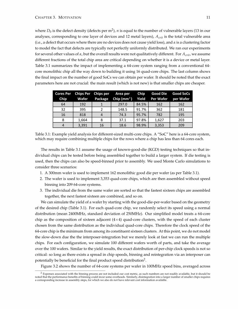
where D0 is the defect density (defects per m2), n is equal to the number of vulnerable layers (13 in ouranalyses, corresponding to one layer of devices and 12 metal layers), Acrit is the total vulnerable area(i.e., a defect that occurs where there are no devices does not cause yield loss), and α is a clustering factorto model the fact that defects are typically not perfectly uniformly distributed. We ran our experimentsfor several other values of α, but the overall results were not qualitatively different. For Acrit, we assumedifferent fractions of the total chip area are critical depending on whether it is a device or metal layer.Table 3.1 summarizes the impact of implementing a 64-core system ranging from a conventional 64-core monolithic chip all the way down to building it using 16 quad-core chips. The last column showsthe final impact on the number of good SoCs we can obtain per wafer. It should be noted that the exactparameters here are not crucial: the main result (which is not new) is that smaller chips are cheaper.
Cores Per Chip
Chips Per Wafer
Chips per Package
Area per Chip (mm2)
Chip Yield
Good Die Per Wafer
Good SoCs per Wafer
64 192 1 297.0 84.5% 162 16232 395 2 148.5 91.7% 362 18116 818 4 74.3 95.7% 782 1958 1,664 8 37.1 97.8% 1,627 2034 3,391 16 18.6 98.9% 3,353 209
2
Table 3.1: Example yield analysis for different-sized multi-core chips. A “SoC” here is a 64-core system,which may require combining multiple chips for the rows where a chip has less than 64 cores each.
The results in Table 3.1 assume the usage of known-good-die (KGD) testing techniques so that in-dividual chips can be tested before being assembled together to build a larger system. If die testing isused, then the chips can also be speed-binned prior to assembly. We used Monte Carlo simulations toconsider three scenarios:
1. A 300mm wafer is used to implement 162 monolithic good die per wafer (as per Table 3.1).2. The wafer is used to implement 3,353 quad-core chips, which are then assembled without speed
binning into 209 64-core systems.3. The individual die from the same wafer are sorted so that the fastest sixteen chips are assembled
together, the next fastest sixteen are combined, and so on.We can simulate the yield of a wafer by starting with the good-die-per-wafer based on the geometry
of the desired chip (Table 3.1). For each quad-core chip, we randomly select its speed using a normaldistribution (mean 2400MHz, standard deviation of 250MHz). Our simplified model treats a 64-corechip as the composition of sixteen adjacent (4×4) quad-core clusters, with the speed of each clusterchosen from the same distribution as the individual quad-core chips. Therefore the clock speed of the64-core chip is the minimum from among its constituent sixteen clusters. At this point, we do not modelthe slow-down due the the interposer-integration but we merely look at fast we can run the multiplechips. For each configuration, we simulate 100 different wafers worth of parts, and take the averageover the 100 wafers. Similar to the yield results, the exact distribution of per-chip clock speeds is not socritical: so long as there exists a spread in chip speeds, binning and reintegration via an interposer canpotentially be beneficial for the final product speed distribution2.
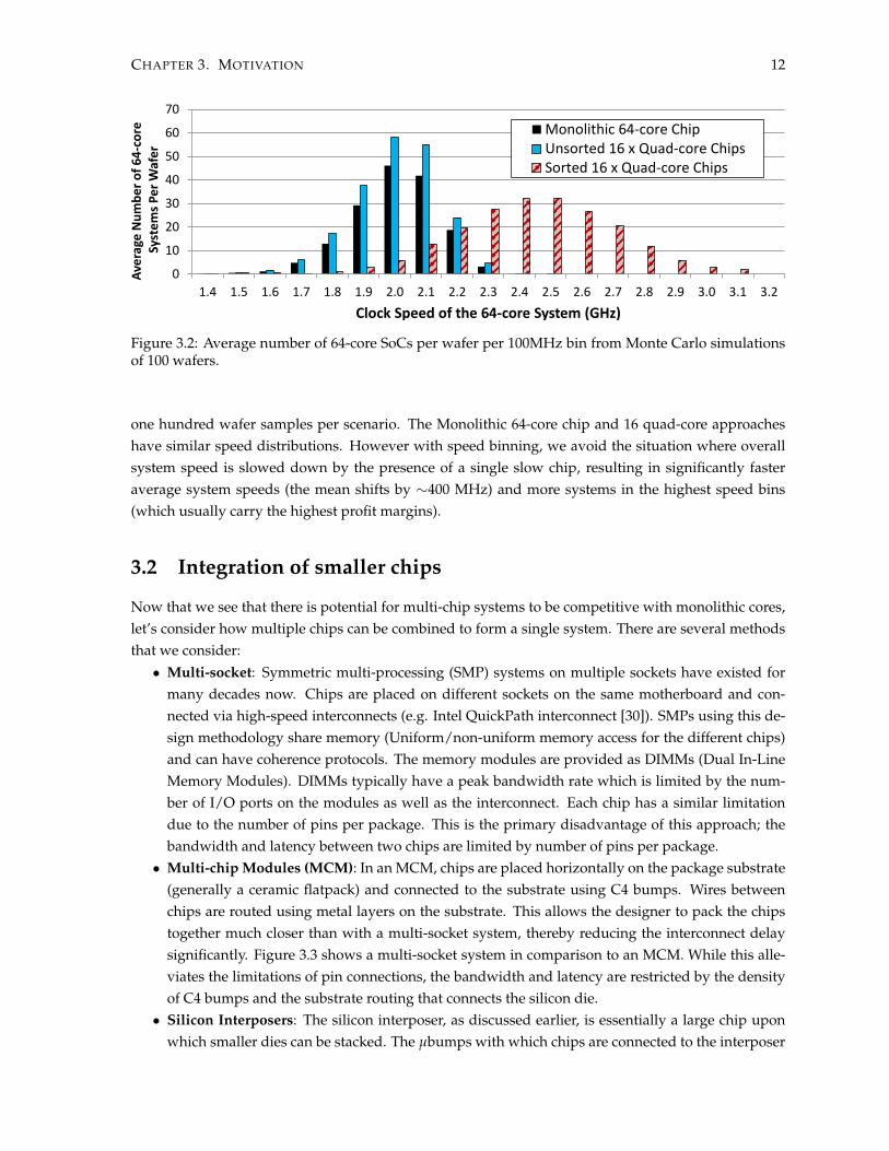
Figure 3.2 shows the number of 64-core systems per wafer in 100MHz speed bins, averaged across
2 Expenses associated with the binning process are not included our cost metric, as such numbers are not readily available, but it should benoted that the performance benefits of binning could incur some overheads. Similarly, disintegration into a larger number of smaller chips requiresa corresponding increase in assembly steps, for which we also do not have relevant cost information available.
CHAPTER 3. MOTIVATION 12
0
10
20
30
40
50
60
70
1.4 1.5 1.6 1.7 1.8 1.9 2.0 2.1 2.2 2.3 2.4 2.5 2.6 2.7 2.8 2.9 3.0 3.1 3.2
Ave
rage
Nu
mb
er
of
64
-co
reSy
ste
ms
Pe
r W
afe
r
Clock Speed of the 64-core System (GHz)
Monolithic 64-core ChipUnsorted 16 x Quad-core ChipsSorted 16 x Quad-core Chips
Figure 3.2: Average number of 64-core SoCs per wafer per 100MHz bin from Monte Carlo simulationsof 100 wafers.
one hundred wafer samples per scenario. The Monolithic 64-core chip and 16 quad-core approacheshave similar speed distributions. However with speed binning, we avoid the situation where overallsystem speed is slowed down by the presence of a single slow chip, resulting in significantly fasteraverage system speeds (the mean shifts by ∼400 MHz) and more systems in the highest speed bins(which usually carry the highest profit margins).
3.2 Integration of smaller chips
Now that we see that there is potential for multi-chip systems to be competitive with monolithic cores,let’s consider how multiple chips can be combined to form a single system. There are several methodsthat we consider:• Multi-socket: Symmetric multi-processing (SMP) systems on multiple sockets have existed for
many decades now. Chips are placed on different sockets on the same motherboard and con-nected via high-speed interconnects (e.g. Intel QuickPath interconnect [30]). SMPs using this de-sign methodology share memory (Uniform/non-uniform memory access for the different chips)and can have coherence protocols. The memory modules are provided as DIMMs (Dual In-LineMemory Modules). DIMMs typically have a peak bandwidth rate which is limited by the num-ber of I/O ports on the modules as well as the interconnect. Each chip has a similar limitationdue to the number of pins per package. This is the primary disadvantage of this approach; thebandwidth and latency between two chips are limited by number of pins per package.
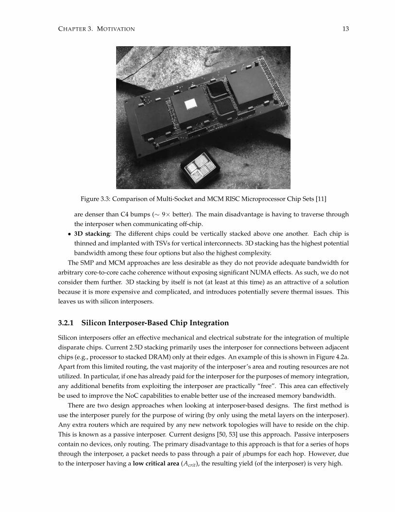
• Multi-chip Modules (MCM): In an MCM, chips are placed horizontally on the package substrate(generally a ceramic flatpack) and connected to the substrate using C4 bumps. Wires betweenchips are routed using metal layers on the substrate. This allows the designer to pack the chipstogether much closer than with a multi-socket system, thereby reducing the interconnect delaysignificantly. Figure 3.3 shows a multi-socket system in comparison to an MCM. While this alle-viates the limitations of pin connections, the bandwidth and latency are restricted by the densityof C4 bumps and the substrate routing that connects the silicon die.
• Silicon Interposers: The silicon interposer, as discussed earlier, is essentially a large chip uponwhich smaller dies can be stacked. The µbumps with which chips are connected to the interposer
CHAPTER 3. MOTIVATION 13
Multichip Modules (MCMs)
INTEGRATED CIRCUIT ENGINEERING CORPORATION 12-13
Source: nChip/ICE, “Roadmaps of Packaging Technology” 15882
Figure 12-18. Comparison of Conventional and MCM RISC Microprocessor Chip Sets
Figure 12-19. Thin-Film Multichip Modules and Equivalent Single-Chip Packages
Source: Advanced Packaging Systems/ICE, “Roadmaps of Packaging Technology” 16208
Figure 3.3: Comparison of Multi-Socket and MCM RISC Microprocessor Chip Sets [11]
are denser than C4 bumps (∼ 9× better). The main disadvantage is having to traverse throughthe interposer when communicating off-chip.
• 3D stacking: The different chips could be vertically stacked above one another. Each chip isthinned and implanted with TSVs for vertical interconnects. 3D stacking has the highest potentialbandwidth among these four options but also the highest complexity.
The SMP and MCM approaches are less desirable as they do not provide adequate bandwidth forarbitrary core-to-core cache coherence without exposing significant NUMA effects. As such, we do notconsider them further. 3D stacking by itself is not (at least at this time) as an attractive of a solutionbecause it is more expensive and complicated, and introduces potentially severe thermal issues. Thisleaves us with silicon interposers.
3.2.1 Silicon Interposer-Based Chip Integration
Silicon interposers offer an effective mechanical and electrical substrate for the integration of multipledisparate chips. Current 2.5D stacking primarily uses the interposer for connections between adjacentchips (e.g., processor to stacked DRAM) only at their edges. An example of this is shown in Figure 4.2a.Apart from this limited routing, the vast majority of the interposer’s area and routing resources are notutilized. In particular, if one has already paid for the interposer for the purposes of memory integration,any additional benefits from exploiting the interposer are practically “free”. This area can effectivelybe used to improve the NoC capabilities to enable better use of the increased memory bandwidth.
There are two design approaches when looking at interposer-based designs. The first method isuse the interposer purely for the purpose of wiring (by only using the metal layers on the interposer).Any extra routers which are required by any new network topologies will have to reside on the chip.This is known as a passive interposer. Current designs [50, 53] use this approach. Passive interposerscontain no devices, only routing. The primary disadvantage to this approach is that for a series of hopsthrough the interposer, a packet needs to pass through a pair of µbumps for each hop. However, dueto the interposer having a low critical area (Acrit), the resulting yield (of the interposer) is very high.
CHAPTER 3. MOTIVATION 14
Parameter Value
n 13
Fraccrit (wire) 0.2625
Fraccrit (logic) 0.7500
a 1.5
Table 3.2: Parameters for thechip yield calculations
D0 500 1000 1500 2000 2500
Passive 98.5% 97.0% 95.5% 94.1% 92.7%
Active 1% 98.4% 96.9% 95.4% 93.9% 92.5%
Active 10% 98.0% 96.1% 94.2% 92.4% 90.7%
Fully-active 87.2% 76.9% 68.5% 61.5% 55.6%
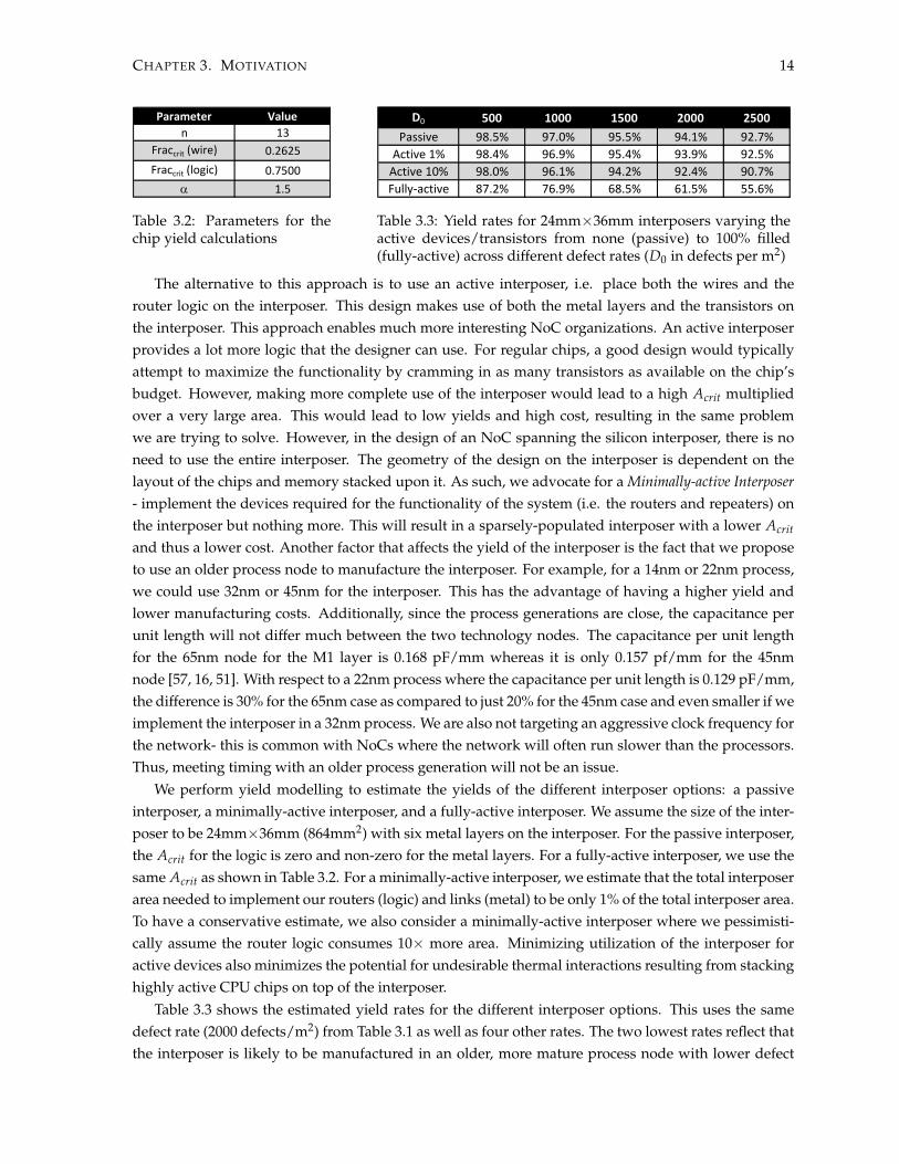
Table 3.3: Yield rates for 24mm×36mm interposers varying theactive devices/transistors from none (passive) to 100% filled(fully-active) across different defect rates (D0 in defects per m2)
The alternative to this approach is to use an active interposer, i.e. place both the wires and therouter logic on the interposer. This design makes use of both the metal layers and the transistors onthe interposer. This approach enables much more interesting NoC organizations. An active interposerprovides a lot more logic that the designer can use. For regular chips, a good design would typicallyattempt to maximize the functionality by cramming in as many transistors as available on the chip’sbudget. However, making more complete use of the interposer would lead to a high Acrit multipliedover a very large area. This would lead to low yields and high cost, resulting in the same problemwe are trying to solve. However, in the design of an NoC spanning the silicon interposer, there is noneed to use the entire interposer. The geometry of the design on the interposer is dependent on thelayout of the chips and memory stacked upon it. As such, we advocate for a Minimally-active Interposer- implement the devices required for the functionality of the system (i.e. the routers and repeaters) onthe interposer but nothing more. This will result in a sparsely-populated interposer with a lower Acrit
and thus a lower cost. Another factor that affects the yield of the interposer is the fact that we proposeto use an older process node to manufacture the interposer. For example, for a 14nm or 22nm process,we could use 32nm or 45nm for the interposer. This has the advantage of having a higher yield andlower manufacturing costs. Additionally, since the process generations are close, the capacitance perunit length will not differ much between the two technology nodes. The capacitance per unit lengthfor the 65nm node for the M1 layer is 0.168 pF/mm whereas it is only 0.157 pf/mm for the 45nmnode [57, 16, 51]. With respect to a 22nm process where the capacitance per unit length is 0.129 pF/mm,the difference is 30% for the 65nm case as compared to just 20% for the 45nm case and even smaller if weimplement the interposer in a 32nm process. We are also not targeting an aggressive clock frequency forthe network- this is common with NoCs where the network will often run slower than the processors.Thus, meeting timing with an older process generation will not be an issue.
We perform yield modelling to estimate the yields of the different interposer options: a passiveinterposer, a minimally-active interposer, and a fully-active interposer. We assume the size of the inter-poser to be 24mm×36mm (864mm2) with six metal layers on the interposer. For the passive interposer,the Acrit for the logic is zero and non-zero for the metal layers. For a fully-active interposer, we use thesame Acrit as shown in Table 3.2. For a minimally-active interposer, we estimate that the total interposerarea needed to implement our routers (logic) and links (metal) to be only 1% of the total interposer area.To have a conservative estimate, we also consider a minimally-active interposer where we pessimisti-cally assume the router logic consumes 10× more area. Minimizing utilization of the interposer foractive devices also minimizes the potential for undesirable thermal interactions resulting from stackinghighly active CPU chips on top of the interposer.
Table 3.3 shows the estimated yield rates for the different interposer options. This uses the samedefect rate (2000 defects/m2) from Table 3.1 as well as four other rates. The two lowest rates reflect thatthe interposer is likely to be manufactured in an older, more mature process node with lower defect
CHAPTER 3. MOTIVATION 15
0.7
0.8
0.9
1.0
64 32 16 8 4
No
rma
lize
d C
os
t / M
es
sa
ge
La
ten
cy
(lo
we
r is
be
tte
r)
Cores per Chip
D=1500
D=2000
D=2500
Avg. Latency
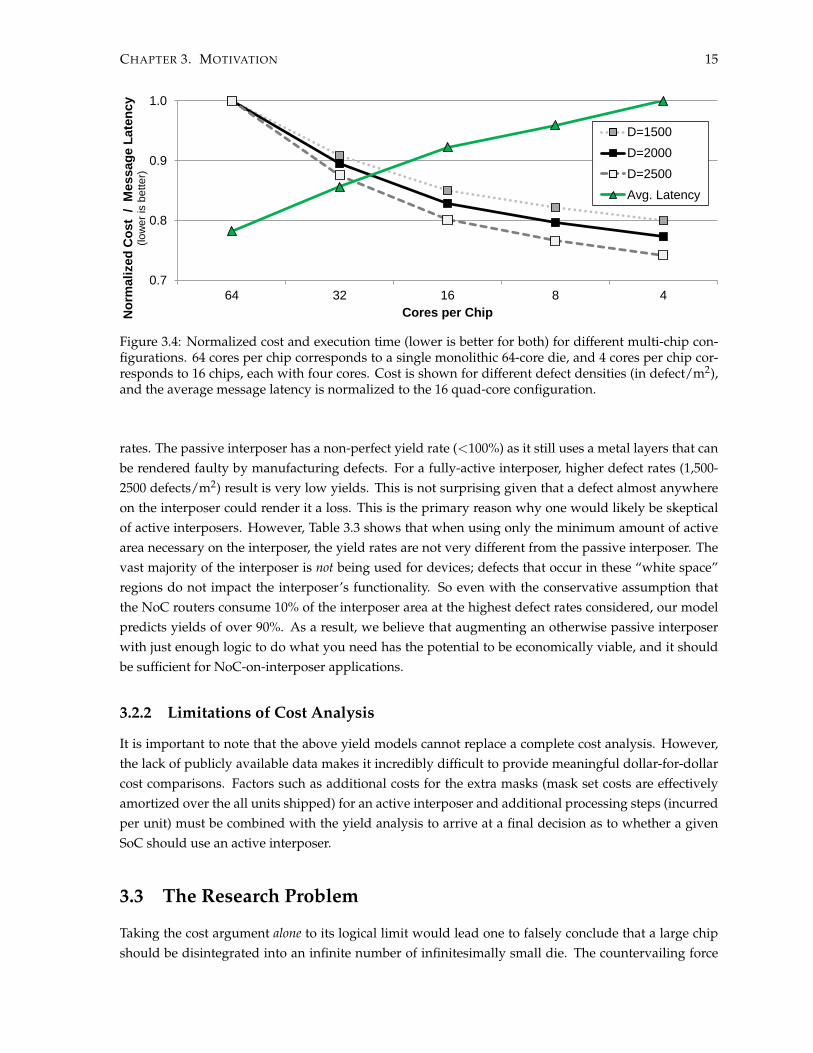
Figure 3.4: Normalized cost and execution time (lower is better for both) for different multi-chip con-figurations. 64 cores per chip corresponds to a single monolithic 64-core die, and 4 cores per chip cor-responds to 16 chips, each with four cores. Cost is shown for different defect densities (in defect/m2),and the average message latency is normalized to the 16 quad-core configuration.
rates. The passive interposer has a non-perfect yield rate (<100%) as it still uses a metal layers that canbe rendered faulty by manufacturing defects. For a fully-active interposer, higher defect rates (1,500-2500 defects/m2) result is very low yields. This is not surprising given that a defect almost anywhereon the interposer could render it a loss. This is the primary reason why one would likely be skepticalof active interposers. However, Table 3.3 shows that when using only the minimum amount of activearea necessary on the interposer, the yield rates are not very different from the passive interposer. Thevast majority of the interposer is not being used for devices; defects that occur in these “white space”regions do not impact the interposer’s functionality. So even with the conservative assumption thatthe NoC routers consume 10% of the interposer area at the highest defect rates considered, our modelpredicts yields of over 90%. As a result, we believe that augmenting an otherwise passive interposerwith just enough logic to do what you need has the potential to be economically viable, and it shouldbe sufficient for NoC-on-interposer applications.
3.2.2 Limitations of Cost Analysis
It is important to note that the above yield models cannot replace a complete cost analysis. However,the lack of publicly available data makes it incredibly difficult to provide meaningful dollar-for-dollarcost comparisons. Factors such as additional costs for the extra masks (mask set costs are effectivelyamortized over the all units shipped) for an active interposer and additional processing steps (incurredper unit) must be combined with the yield analysis to arrive at a final decision as to whether a givenSoC should use an active interposer.
3.3 The Research Problem
Taking the cost argument alone to its logical limit would lead one to falsely conclude that a large chipshould be disintegrated into an infinite number of infinitesimally small die. The countervailing force

CHAPTER 3. MOTIVATION 16
is performance. While breaking a large system into smaller pieces may improve overall yield, goingto a larger number of smaller chips increases the amount of chip-to-chip communication that must berouted through the interposer. In an interposer-based multi-core system with a NoC distributed acrosschips and the interposer, smaller chips create a more fragmented NoC resulting in more core-to-coretraffic routing across the interposer, which eventually becomes a performance bottleneck. Figure 3.4shows the cost reduction for three different defect rates, all showing the relative cost benefit of disinte-gration. The figure also shows the relative impact on performance3. So while more aggressive levels ofdisintegration provide better cost savings, it is directly offset by a reduction in performance.
The problem we explore is how we can get the cost benefits of a disintegrated chip organizationwhile providing an NoC architecture that still behaves similarly in terms of performance to one imple-mented on a single monolithic chip. We aim to do this by utilizing the additional resources availableon the interposer to design networks specifically for 2.5D systems instead of just using edge-to-edgeconnections. These new networks will utilize resources on both the interposer and on each of the chips.This allows for a variety of optimizations which can help reduce the average number of hops betweendifferent cores as well as to memory. We can also route packets in such a way so as to distribute the net-work load across the resources on and off-chip. We discuss the challenges and our proposal to addressthem in Chapter 4.
3 We show the average message latency for all traffic (coherence and main memory) in a synthetic uniform-distribution workload, where CPUchips and the interposer respectively use 2D meshes vertically connected through µbumps. See Chapter 5 for full details.
Chapter 4
NoC Architecture
4.1 Baseline Architecture
The baseline design that we serves as the starting point of our design is shown in Figure 4.1. Thisarchitecture is a 2.5D system with four 16-core CPU chips. The interposer in this design is relativelylarge but fits within an assumed reticle limit of 24mm×36mm. On the interposer are four 16-core chipsas well as four 3D DRAM stacks. Each chip is of the size 7.75mm × 7.75mm. The DRAM stacks (eachof size 8.75mm × 8.75mm) are placed on either side of the multi-core die. Each of these four stacks areassumed to have a size similar to a JEDEC Wide-IO DRAM [33, 37]. Each stack has four channels1, with16 channels in total. The chip-to-chip spacing is assumed to be 0.5mm for all pairs shown in the figure.
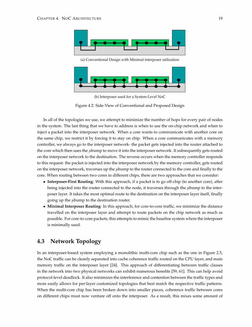
Current 2.5D designs utilize the interposer for chip-to-chip routing and for vertical connections tothe package substrate for power, ground, and I/O [53]. In current industry designs, the interposeris used minimally. Therefore, we decided to use a passive interposer for the baseline design. In thisdesign, the DRAM stacks are integrated with four 16-core multi-core chips on a passive interposer.There are only edge-to-edge connections between the multiple chips as shown in Figure 4.2a.
Our proposal seeks to make use of the unused routing resources available on the interposer layerto implement a system-level NoC. This concept is illustrated in Figure 4.2b. Thus, in addition to theon-chip network, there is a secondary (logical) 10× 8 mesh network on the interposer which connectsthe various chips as well as the four DRAM stacks where each core has its own link into the interposer.Each core in each of the four chips has a connection (through µbumps) to the the interposer layer,totalling 16 connections per each multi-core chip and four connections for each DRAM stack (one foreach memory channel).
4.2 Routing Protocol
When a core wants to communicate off-chip (either with a core on another chip or with memory), ithas to use the interposer network or a combination of the on-chip and the interposer network to reachits destination. There are many cases where there are multiple possible paths that a packet could takefrom source to destination. The quality of a path can be measured by the number of hops requiredfor a packet to be routed from the source to the destination. A lower hop count implies that a packet
1Having multiple channels for each DRAM memory stack increases the maximum bandwidth of the memory module.
17

CHAPTER 4. NOC ARCHITECTURE 18
36mm
24mm
8.75mm
8.75mm
0.5mm
7.75mm
3D-DRAM
16-corechipSiliconInterposerFigure 4.1: Top View of evaluated 2.5D multi-core system with four DRAM stacks placed on either sideof the processor dies
can reach the destination in fewer steps. The hop count directly influences the average packet latencywhich is a good indicator of the network performance. For a given network, varying the routing pro-tocol can have an effect on the system performance. In most cases, we can statically determine theminimal paths (in terms of hop count and latency). However, in certain cases, there are multiple mini-mal paths. Therefore, it becomes imperative to specify a routing protocol which can be used to resolvesuch ambiguities.
For standard 2D mesh-based NoCs, the most common routing protocol is Dimension Order Routing(DOR). DOR can either be XY or YX for 2D networks. DOR-XY first routes a packet along the horizontallinks (through the shortest path) to the appropriate column. It then routes the packet vertically (again,along the shortest path) until it reaches its destination. DOR-YX routes vertically first and then hori-zontally. When we look at 2.5D networks, we are adding a third dimension. There are two ways wecan look at these networks. The first is to look at the system as two separate NoCs and provide a rout-ing protocol for each independently and have an overseeing protocol which controls when a packetswitches between the two networks. The second is to consider the network as a 3-dimensional networkwith the vertical links constituting the Z-axis. For simpler network topologies, the second approach issimpler since it does not require any modification of earlier protocols. However, we will use the firstmethod since it allows finer control of resource utilization on the interposer and on chip. This allows usto specify the routing protocol for the on chip network, the interposer network, and when (and where)packets switch between the two sub-networks.
For the on-chip component, all architectures that we use in thesis are a standard mesh and thuswe use simple DOR-XY routing. For the interposer component, mesh-based topologies use DOR-XY.The double butterfly uses extended destination tag routing [2]. The ButterDonut topology (Subsec-tion 4.3.2) uses table-based routing.
CHAPTER 4. NOC ARCHITECTURE 19
(a) Conventional Design with Minimal interposer utilization
(b) Interposer used for a System-Level NoC
Figure 4.2: Side-View of Conventional and Proposed Design
In all of the topologies we use, we attempt to minimize the number of hops for every pair of nodesin the system. The last thing that we have to address is when to use the on-chip network and when toinject a packet into the interposer network. When a core wants to communicate with another core onthe same chip, we restrict it by forcing it to stay on chip. When a core communicates with a memorycontroller, we always go to the interposer network- the packet gets injected into the router attached tothe core which then uses the µbump to move it into the interposer network. It subsequently gets routedon the interposer network to the destination. The reverse occurs when the memory controller respondsto this request: the packet is injected into the interposer network by the memory controller, gets routedon the interposer network, traverses up the µbump to the router connected to the core and finally to thecore. When routing between two cores in different chips, there are two approaches that we consider:
• Interposer-First Routing: With this approach, if a packet is to go off-chip (to another core), afterbeing injected into the router connected to the node, it traverses through the µbump to the inter-poser layer. It takes the most optimal route to the destination on the interposer layer itself, finallygoing up the µbump to the destination router.
• Minimal Interposer Routing: In this approach, for core-to-core traffic, we minimize the distancetravelled on the interposer layer and attempt to route packets on the chip network as much aspossible. For core-to-core packets, this attempts to mimic the baseline system where the interposeris minimally used.
4.3 Network Topology
In an interposer-based system employing a monolithic multi-core chip such as the one in Figure 2.5,the NoC traffic can be cleanly separated into cache coherence traffic routed on the CPU layer, and mainmemory traffic on the interposer layer [24]. This approach of differentiating between traffic classesin the network into two physical networks can exhibit numerous benefits [59, 61]. This can help avoidprotocol-level deadlock. It also minimizes the interference and contention between the traffic types andmore easily allows for per-layer customized topologies that best match the respective traffic patterns.When the multi-core chip has been broken down into smaller pieces, coherence traffic between coreson different chips must now venture off onto the interposer. As a result, this mixes some amount of
CHAPTER 4. NOC ARCHITECTURE 20
Lin
k U
tiliz
atio
n
(a) (c) (b)
Monolithic 64-core chip on 2D Mesh
4x 16-core chips on 2D Mesh
4x 16-core chips on Concentrated Mesh
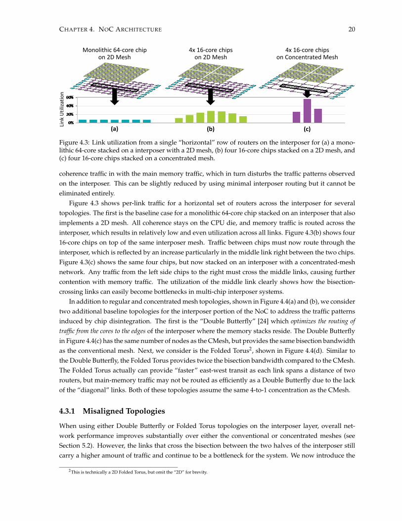
Figure 4.3: Link utilization from a single “horizontal” row of routers on the interposer for (a) a mono-lithic 64-core stacked on a interposer with a 2D mesh, (b) four 16-core chips stacked on a 2D mesh, and(c) four 16-core chips stacked on a concentrated mesh.
coherence traffic in with the main memory traffic, which in turn disturbs the traffic patterns observedon the interposer. This can be slightly reduced by using minimal interposer routing but it cannot beeliminated entirely.
Figure 4.3 shows per-link traffic for a horizontal set of routers across the interposer for severaltopologies. The first is the baseline case for a monolithic 64-core chip stacked on an interposer that alsoimplements a 2D mesh. All coherence stays on the CPU die, and memory traffic is routed across theinterposer, which results in relatively low and even utilization across all links. Figure 4.3(b) shows four16-core chips on top of the same interposer mesh. Traffic between chips must now route through theinterposer, which is reflected by an increase particularly in the middle link right between the two chips.Figure 4.3(c) shows the same four chips, but now stacked on an interposer with a concentrated-meshnetwork. Any traffic from the left side chips to the right must cross the middle links, causing furthercontention with memory traffic. The utilization of the middle link clearly shows how the bisection-crossing links can easily become bottlenecks in multi-chip interposer systems.
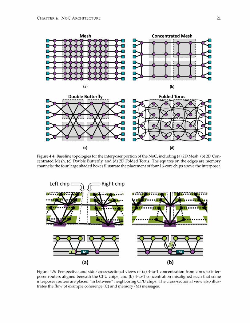
In addition to regular and concentrated mesh topologies, shown in Figure 4.4(a) and (b), we considertwo additional baseline topologies for the interposer portion of the NoC to address the traffic patternsinduced by chip disintegration. The first is the “Double Butterfly” [24] which optimizes the routing oftraffic from the cores to the edges of the interposer where the memory stacks reside. The Double Butterflyin Figure 4.4(c) has the same number of nodes as the CMesh, but provides the same bisection bandwidthas the conventional mesh. Next, we consider is the Folded Torus2, shown in Figure 4.4(d). Similar tothe Double Butterfly, the Folded Torus provides twice the bisection bandwidth compared to the CMesh.The Folded Torus actually can provide “faster” east-west transit as each link spans a distance of tworouters, but main-memory traffic may not be routed as efficiently as a Double Butterfly due to the lackof the “diagonal” links. Both of these topologies assume the same 4-to-1 concentration as the CMesh.
4.3.1 Misaligned Topologies
When using either Double Butterfly or Folded Torus topologies on the interposer layer, overall net-work performance improves substantially over either the conventional or concentrated meshes (seeSection 5.2). However, the links that cross the bisection between the two halves of the interposer stillcarry a higher amount of traffic and continue to be a bottleneck for the system. We now introduce the
2This is technically a 2D Folded Torus, but omit the “2D” for brevity.
CHAPTER 4. NOC ARCHITECTURE 21
(c) (d)
(a) (b)
Mesh Concentrated Mesh
Double Butterfly Folded Torus
Figure 4.4: Baseline topologies for the interposer portion of the NoC, including (a) 2D Mesh, (b) 2D Con-centrated Mesh, (c) Double Butterfly, and (d) 2D Folded Torus. The squares on the edges are memorychannels; the four large shaded boxes illustrate the placement of four 16-core chips above the interposer.
(a) (b)
C M M
Left chip Right chip
Figure 4.5: Perspective and side/cross-sectional views of (a) 4-to-1 concentration from cores to inter-poser routers aligned beneath the CPU chips, and (b) 4-to-1 concentration misaligned such that someinterposer routers are placed “in between” neighboring CPU chips. The cross-sectional view also illus-trates the flow of example coherence (C) and memory (M) messages.
CHAPTER 4. NOC ARCHITECTURE 22
(a) (b) (c)
Folded Torus(X) Folded Torus(X+Y) Double Butterfly (X)
Figure 4.6: Example implementations of misaligned interposer NoC topologies: Folded Torus mis-aligned in the (a) X-dimension only, (b) both X and Y, and (c) a Double Butterfly misaligned in theX-dimension.
concept of a “misaligned” interposer topology. For our concentrated topologies thus far, every fourCPU cores in a 2×2 grid share an interposer router that was placed in between them, as shown in bothperspective and side/cross-sectional views in Figure 4.5(a). So for a 4×4 16-core chip, there would befour “concentrating” router nodes aligned directly below each quadrant of the CPU chip.
A misaligned interposer network offsets the location of the interposer routers. Cores on the edge ofone chip now share a router with cores on the edge of the adjacent chip as shown in Figure 4.5(b). Thechange is subtle but important: with an “aligned” interposer NoC, the key resources shared betweenchip-to-chip coherence and memory traffic are the links crossing the bisection line, as shown in thebottom of Figure 4.5(a). If both a memory-bound message (M) and a core-to-core coherence message(C) wish to traverse the link, then one must wait as it serializes behind the other. With misalignedtopologies, the shared resource is now the router. As shown in the bottom of Figure 4.5(b), this simpleshift allows chip-to-chip and memory traffic to flow through a router simultaneously, thereby reducingqueuing delays for messages to traverse the network’s bisection cut.
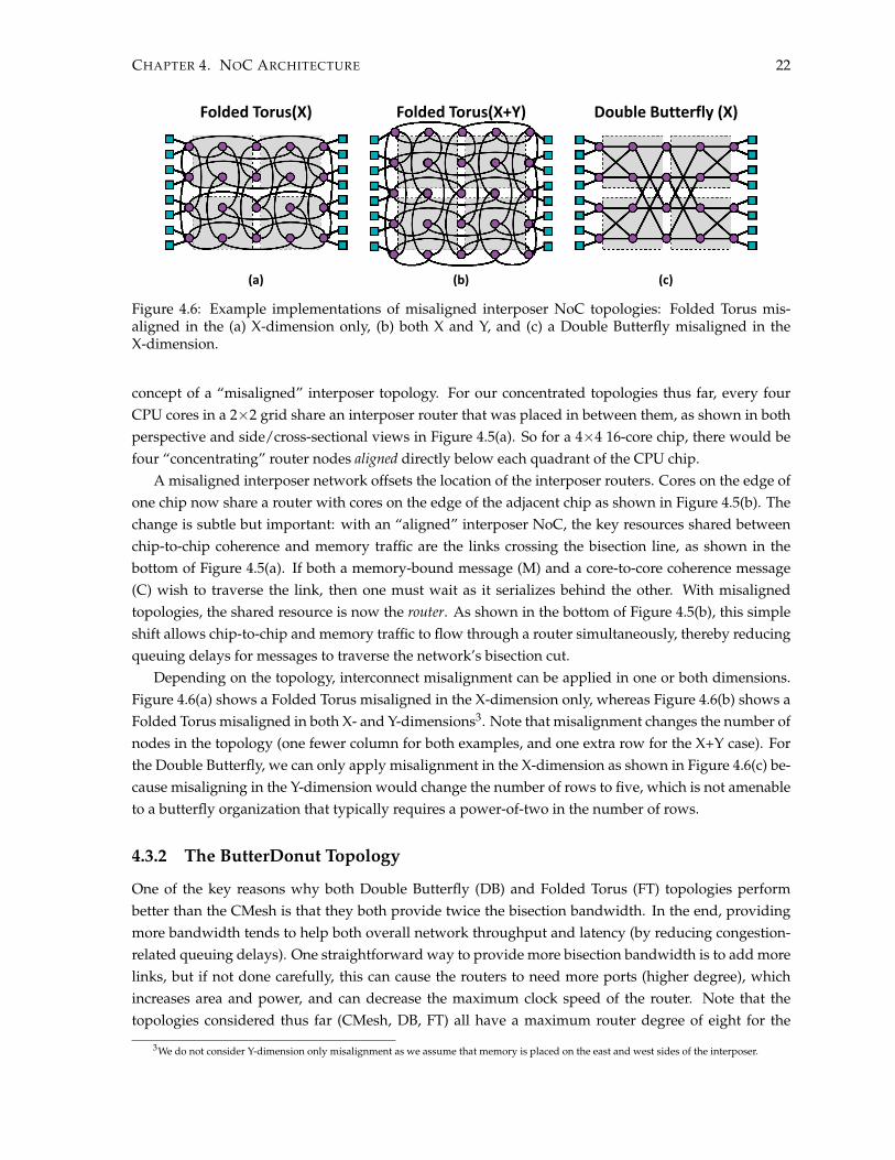
Depending on the topology, interconnect misalignment can be applied in one or both dimensions.Figure 4.6(a) shows a Folded Torus misaligned in the X-dimension only, whereas Figure 4.6(b) shows aFolded Torus misaligned in both X- and Y-dimensions3. Note that misalignment changes the number ofnodes in the topology (one fewer column for both examples, and one extra row for the X+Y case). Forthe Double Butterfly, we can only apply misalignment in the X-dimension as shown in Figure 4.6(c) be-cause misaligning in the Y-dimension would change the number of rows to five, which is not amenableto a butterfly organization that typically requires a power-of-two in the number of rows.
4.3.2 The ButterDonut Topology
One of the key reasons why both Double Butterfly (DB) and Folded Torus (FT) topologies performbetter than the CMesh is that they both provide twice the bisection bandwidth. In the end, providingmore bandwidth tends to help both overall network throughput and latency (by reducing congestion-related queuing delays). One straightforward way to provide more bisection bandwidth is to add morelinks, but if not done carefully, this can cause the routers to need more ports (higher degree), whichincreases area and power, and can decrease the maximum clock speed of the router. Note that thetopologies considered thus far (CMesh, DB, FT) all have a maximum router degree of eight for the
3We do not consider Y-dimension only misalignment as we assume that memory is placed on the east and west sides of the interposer.
CHAPTER 4. NOC ARCHITECTURE 23
(a) (b)
ButterDonut Misaligned ButterDonut(X)
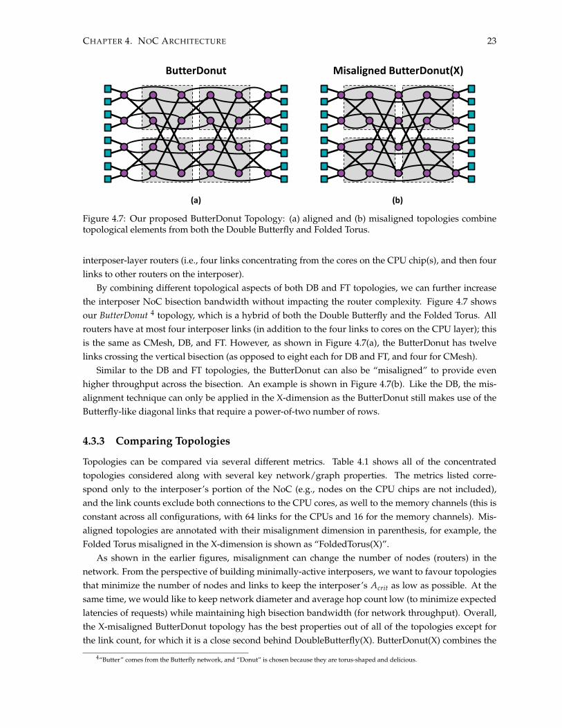
Figure 4.7: Our proposed ButterDonut Topology: (a) aligned and (b) misaligned topologies combinetopological elements from both the Double Butterfly and Folded Torus.
interposer-layer routers (i.e., four links concentrating from the cores on the CPU chip(s), and then fourlinks to other routers on the interposer).
By combining different topological aspects of both DB and FT topologies, we can further increasethe interposer NoC bisection bandwidth without impacting the router complexity. Figure 4.7 showsour ButterDonut 4 topology, which is a hybrid of both the Double Butterfly and the Folded Torus. Allrouters have at most four interposer links (in addition to the four links to cores on the CPU layer); thisis the same as CMesh, DB, and FT. However, as shown in Figure 4.7(a), the ButterDonut has twelvelinks crossing the vertical bisection (as opposed to eight each for DB and FT, and four for CMesh).
Similar to the DB and FT topologies, the ButterDonut can also be “misaligned” to provide evenhigher throughput across the bisection. An example is shown in Figure 4.7(b). Like the DB, the mis-alignment technique can only be applied in the X-dimension as the ButterDonut still makes use of theButterfly-like diagonal links that require a power-of-two number of rows.
4.3.3 Comparing Topologies
Topologies can be compared via several different metrics. Table 4.1 shows all of the concentratedtopologies considered along with several key network/graph properties. The metrics listed corre-spond only to the interposer’s portion of the NoC (e.g., nodes on the CPU chips are not included),and the link counts exclude both connections to the CPU cores, as well to the memory channels (this isconstant across all configurations, with 64 links for the CPUs and 16 for the memory channels). Mis-aligned topologies are annotated with their misalignment dimension in parenthesis, for example, theFolded Torus misaligned in the X-dimension is shown as “FoldedTorus(X)”.
As shown in the earlier figures, misalignment can change the number of nodes (routers) in thenetwork. From the perspective of building minimally-active interposers, we want to favour topologiesthat minimize the number of nodes and links to keep the interposer’s Acrit as low as possible. At thesame time, we would like to keep network diameter and average hop count low (to minimize expectedlatencies of requests) while maintaining high bisection bandwidth (for network throughput). Overall,the X-misaligned ButterDonut topology has the best properties out of all of the topologies except forthe link count, for which it is a close second behind DoubleButterfly(X). ButterDonut(X) combines the
4“Butter” comes from the Butterfly network, and “Donut” is chosen because they are torus-shaped and delicious.

CHAPTER 4. NOC ARCHITECTURE 24
Topology Nodes Links Diameter Avg Hop Bisection Links
CMesh 24 (6x4) 38 8 3.33 4
DoubleButterfly 24 (6x4) 40 5 2.70 8
FoldedTorus 24 (6x4) 48 5 2.61 8
ButterDonut 24 (6x4) 44 4 2.51 12
FoldedTorus(X) 20 (5x4) 40 4 2.32 8
DoubleButterfly(X) 20 (5x4) 32 4 2.59 8
FoldedTorus(XY) 25 (5x5) 50 4 2.50 10
ButterDonut(X) 20 (5x4) 36 4 2.32 12Mis
alig
ned
Table 4.1: Comparison of the different interposer NoC topologies studied in this paper. In the nodecolumn, n×m in parenthesis indicates the organization of router nodes. Bisection Links are the numberof links crossing the vertical bisection cut.
best of all of the other non-ButterDonut topologies, while providing 50% more bisection bandwidth.
4.3.4 Deadlock Freedom
The Folded Torus and ButterDonut topologies are susceptible to network-level deadlock due to thepresence of rings within a dimension (either along the X-axis or the Y-axis) of the topology. Two con-ventional approaches have been widely employed to avoid deadlock in torus networks: virtual chan-nels [2] and bubble flow control [48]. Virtual channels (VCs) are separate buffers/queues which sharethe physical link in a router. An escape virtual channel can be used to ensure deadlock freedom. Inan escape VC, a deadlock-free routing function is used (usually by restricting certain turns). When apacket is stuck in the network for a certain period of time (when it is under deadlock), it moves intothe escape VC which it can use to reach the destination without another chance of deadlocking. In thiswork, we leverage recently proposed flit-level bubble flow control [15, 44] to avoid deadlock in theserings. However, with torus-based networks, even by restricting turns, there are rings in a single dimen-sion which has the potential to form a deadlock cycle. Bubble Flow Control [48] is a flow control protocoltargeted at these types of networks to mitigate this issue and it does so using just a single virtual chan-nel. Puente et al. show that for wormhole switching in a torus-based network, each uni-directional ringis deadlock-free if there exists at least one worm-bubble located anywhere in the ring after packet injec-tion. As the ButterDonut topology only has rings in the x-dimension, bubble flow control is applied inthat dimension only and typical wormhole is applied for packets transiting through the y-dimension5.
4.4 Physical implementation
As discussed in Section 3.2.1, we advocate for a minimally-active interposer. To implement the NoCon an active interposer6, we simply place both the NoC links (wires) and the routers (transistors) on
5 This discussion treats diagonal links as y-dimension links. For the Folded Torus, bubble flow control must be applied in both dimensions.As strict dimension order routing cannot be used in the ButterDonut topology (packets can change from x to y and from y to x dimensions), anadditional virtual channel is required. We modify the original routing algorithm for the DoubleButterfly networks [24]; routes that double-back(head E-W and then W-E on other links) are not possible due to disintegration. Table-based routing based on extended destination tag routingcoupled with extra VCs maintain deadlock freedom for these topologies.
6Current publicly-known designs have not implemented an active interposer but we believe there is a strong case for it in the future.

CHAPTER 4. NOC ARCHITECTURE 25
Router on active interposer
Router on CPU die
All logic/gates on CPU die
Only metal routing on passive interposer
(a)
(b)
CPU Die
Interposer
CPU Die
Interposer
Figure 4.8: (a) Implementation of a NoC with routers on both the CPU die and an active interposer, and(b) an implementation where all routing logic is on the CPU die, and a passive interposer only providesthe interconnect wiring for the interposer’s portion of the NoC.
the interposer layer. However, most current implementations use a passive interposer. Figure 4.8(a)shows a small example NoC with the interposer layer’s partition of the NoC completely implementedon the interposer. For the near future, however, it is expected that only passive, device-less interposerswill be commonly used. Figure 4.8(b) shows an implementation where the active components of therouter (e.g., buffers, arbiters) are placed on the CPU die, but the NoC links (e.g., 128 bits/direction)still utilize the interposer’s routing resources. This approach enables the utilization of the interposer’smetal layers for NoC routing at the cost of some area on the CPU die to implement the NoC’s logiccomponents.7 Both NoCs in Figure 4.8 are topologically and functionally identical, but have differentphysical organizations to match the capabilities (or lack thereof) of their respective interposers.
4.4.1 µbump Overheads
We assume a µbump pitch of 45µm [53]. For a 128-bit bi-directional NoC link, we would need 270signals (128 bits for data and 7 bits of side-band control signals in each direction) taking up 0.55mm2 ofarea. For an active interposer, each node on the chip requires one set of vertical interconnects. For each16-core chip, this will take up 8.8mm2 of area (from the top metal layer) which amounts to less than15% of the CPU chip area.
For a passive interposer, if the interposer layer is used to implement a mesh of the same size asthe CPU-layer, each node would need to have four such links (for each N/S/E/W direction). Thetotal area overhead for the µbumps for each 16-core chip would be 35.2mm2, or nearly half (58%) ofour assumed 7.75mm×7.75mm multi-core processor die. To reduce the µbump area overheads for apassive-interposer implementation, we use concentration [6]. Every four nodes in the CPU layer’sbasic mesh are concentrated into a single node of the interposer-layer NoC. Figure 4.5 shows differentviews of this. The side view illustrates the interposer nodes as logically being on the interposer layer(for the passive interposer case, the logic and routing are split between the CPU die and the interposeras described earlier). Usage of a concentrated topology for the interposer layer provides a reductionof the µbump overheads by a factor of four, down to 8.8mm2- the same overhead as with an activeinterposer design. Concentration for the active interposer case does not have any benefit since each
7If the “interposer links” are too long and would otherwise require repeaters, the wires can “resurface” back to the active CPU die to berepeated. This requires some additional area on the CPU die for the repeaters as well as any corresponding µbumparea, but this is not significantlydifferent than long conventional wires that also need to be broken up into multiple repeated segments.

CHAPTER 4. NOC ARCHITECTURE 26
node would still require just one set of vertical interconnects- the same as the base case.
Summary
In this chapter, we described the various designs that we proposed, specifically for 2.5D multi-chipinterposer systems. In the next chapter, we explain the methodology we used to evaluate our proposeddesigns and analyze the results from this methodology.
Chapter 5
Methodology and Evaluation
In this chapter, we first describe the methodology used for the evaluation of the NoC designs fromChapter 4. We then do a extensive evaluation using multiple methods including synthetic workloadsas well as full-system simulations. We then present these results and our observations about them.
5.1 Methodology
To comprehensively evaluate our designs, we first tested the various topologies using synthetic trafficon a cycle-level network simulator. We then tested out designs using SynFull [5] workloads. Finally,we looked at Full-System simulations using a cycle-accurate multi-core processor simulator.
5.1.1 Synthetic Workloads
To evaluate the performance of various 2.5D NoC topologies for our disintegrated systems, we useBookSim, a cycle-level network simulator [34], with the configuration parameters listed in Table 5.1.BookSim provides set a basic network topologies, routers, flow control, and arbiters.
Network Topologies and Routing
BookSim does not, by default, support the types of network topologies that we described in Chapter 4.We designed a new method of specifying the various nodes and routers in the system where we canspecify the topology of the chip network as well as the interposer network. The interposer topology, inmost cases, had to be re-defined for each case as they were unique to our design. We also introducedflags to control whether the interposer topology was to be misaligned or not. The size of the chip canalso be varied in terms of the number of nodes along the x-axis and y-axis independently. We alsoenable the specification of its link latency (which is a default parameter) as well as a link priority. Thelink priority is used to generate the routing table: this is done using a minimum-path algorithm. Bychoosing an appropriate set of priorities for each type of link in the system, it is possible to choose be-tween minimal-interposer routing and interposer-first routing. Additionally, we can specify the routingalgorithm for each of the two networks.
27
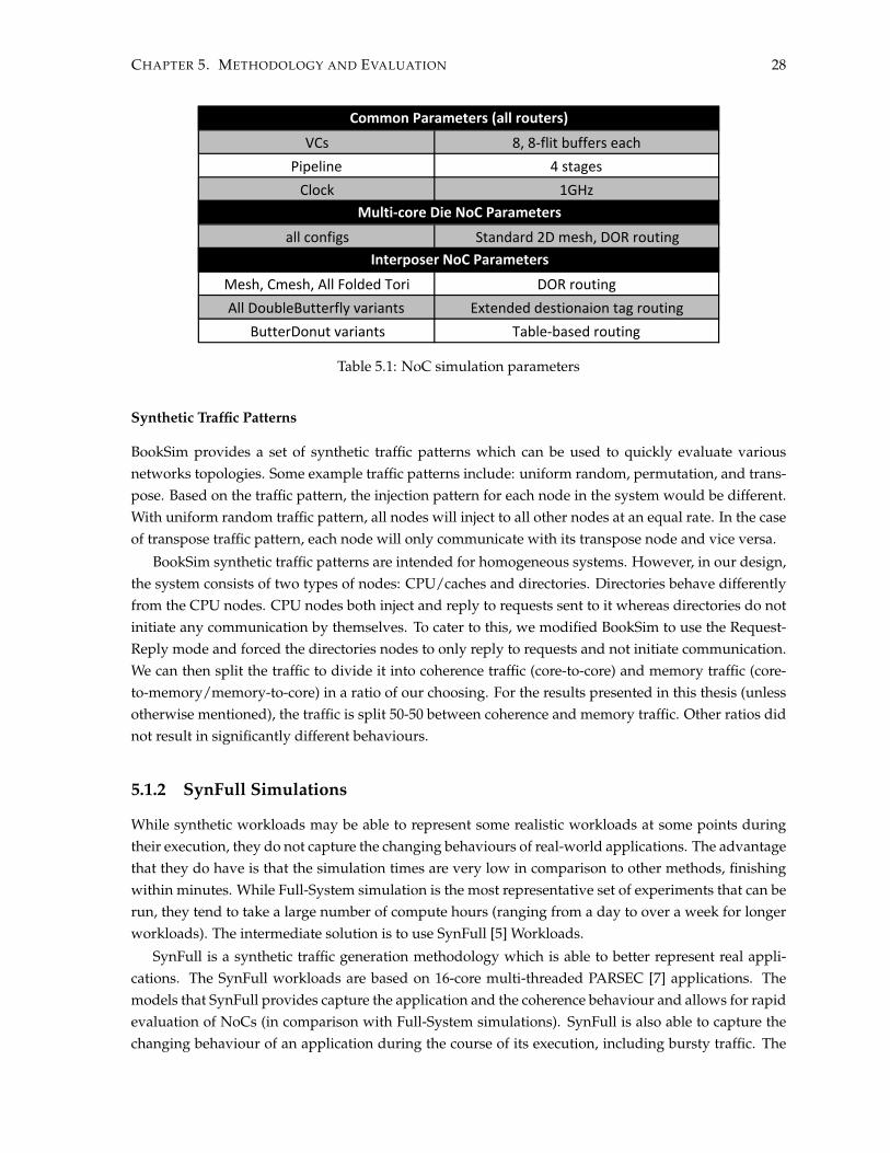
CHAPTER 5. METHODOLOGY AND EVALUATION 28
VCs 8,8-flitbufferseachPipeline 4stagesClock 1GHz
allconfigs Standard2Dmesh,DORrouting
Mesh,Cmesh,AllFoldedTori DORroutingAllDoubleButterflyvariants Extendeddestionaiontagrouting
ButterDonutvariants Table-basedrouting
CommonParameters(allrouters)
Multi-coreDieNoCParameters
InterposerNoCParameters
Table 5.1: NoC simulation parameters
Synthetic Traffic Patterns
BookSim provides a set of synthetic traffic patterns which can be used to quickly evaluate variousnetworks topologies. Some example traffic patterns include: uniform random, permutation, and trans-pose. Based on the traffic pattern, the injection pattern for each node in the system would be different.With uniform random traffic pattern, all nodes will inject to all other nodes at an equal rate. In the caseof transpose traffic pattern, each node will only communicate with its transpose node and vice versa.
BookSim synthetic traffic patterns are intended for homogeneous systems. However, in our design,the system consists of two types of nodes: CPU/caches and directories. Directories behave differentlyfrom the CPU nodes. CPU nodes both inject and reply to requests sent to it whereas directories do notinitiate any communication by themselves. To cater to this, we modified BookSim to use the Request-Reply mode and forced the directories nodes to only reply to requests and not initiate communication.We can then split the traffic to divide it into coherence traffic (core-to-core) and memory traffic (core-to-memory/memory-to-core) in a ratio of our choosing. For the results presented in this thesis (unlessotherwise mentioned), the traffic is split 50-50 between coherence and memory traffic. Other ratios didnot result in significantly different behaviours.
5.1.2 SynFull Simulations
While synthetic workloads may be able to represent some realistic workloads at some points duringtheir execution, they do not capture the changing behaviours of real-world applications. The advantagethat they do have is that the simulation times are very low in comparison to other methods, finishingwithin minutes. While Full-System simulation is the most representative set of experiments that can berun, they tend to take a large number of compute hours (ranging from a day to over a week for longerworkloads). The intermediate solution is to use SynFull [5] Workloads.
SynFull is a synthetic traffic generation methodology which is able to better represent real appli-cations. The SynFull workloads are based on 16-core multi-threaded PARSEC [7] applications. Themodels that SynFull provides capture the application and the coherence behaviour and allows for rapidevaluation of NoCs (in comparison with Full-System simulations). SynFull is also able to capture thechanging behaviour of an application during the course of its execution, including bursty traffic. The

CHAPTER 5. METHODOLOGY AND EVALUATION 29
Chip 4,16-corechips(64coresintotal)Core 2GHz,Out-of-Order,8-wide,192-instructionROB
L1Caches 32kBprivateeachforL1-Instruction,L1-Data,2-wayassocL2Caches 512kBshared,unified,distributedcache,8-wayassoc
CoherenceProtocol Directory-BasedMOESI
Type 4,3D-StackedDRAMChannels 4-channelsperstackDataBus 128-bitBusSpeed 1.6GHz
CPUConfiguration
MemoryConfiguration
Table 5.2: Gem5 Configuration for Full-System Simulation
authors of SynFull [5] provide their source code as well as an interface with BookSim for a 16-core sys-tem. We use SynFull in a multi-programmed environment (with four instances of SynFull) and interfaceit with BookSim. We use a non-trivial mapping of each of the SynFull nodes to our network; the fourinstances are interleaved onto the network so that each 16-core chip has four cores from each instance ofSynFull. This prevents the localization of a single program on to a single chip (which would eliminatechip-to-chip communication). Additionally, we include a simple latency-based memory model for thememory controllers.
As mentioned earlier, the authors provide models for a subset of the PARSEC [7] benchmarks. Wecluster these benchmarks into one of three categories based on the Per-Node Average Accepted PacketRate (for the entire simulation). We denote these clusters as low, medium, and high groups. The highgroup is likely to stress the network more than the medium group.• Low: barnes, blackscholes, bodytrack, cholesky, fluidanimate, lu_cb, raytrace, swaptions, wa-
ter_nsquared, water_spatial• Medium: facesim, radiosity, volrend• High: fft, lu_ncb, radix
Since each of these models only simulates a 16-threaded model, we combine four models to obtain amulti-programmed workload that makes use of all 64 cores in our system. We interleave the threadsfrom the four programs such that each chip has four threads from each program. To obtain eachcombination of four programs, we chose four benchmarks at random from the three groups (L=low,M=medium, H=high) to form a number of workloads. We limited the combinations such that eachworkload falls into one of the following sets: L-L-L-L, M-M-L-L, M-M-M-M, H-H-L-L, H-H-M-M. Wecompute the geometric mean for each set and present them in Subsection 5.2.1.
5.1.3 Full-System Simulations
Full-System simulators simulate all of the cores, caches, and memory sub-system in addition to thenetwork. For our experiments, we use gem5 [9], a cycle-accurate multi-core processor simulator tosimulate the cores, caches, and memory sub-system. We interface gem5 with BookSim [34] and useBookSim as the network simulator. The system configuration is shown in Table 5.2.
We simulate a 64-core SMP system running the Linux kernel version 2.6.28. Each core has it’s ownprivate L1 cache and a slice of the shared L2 cache. There are 16 directories in total. The memorycontrollers are co-located with the directories. The cores, caches, and directories are mapped to their

CHAPTER 5. METHODOLOGY AND EVALUATION 30
corresponding nodes in the network in BookSim. With this setup, we run multi-threaded (with 64threads) versions of the PARSEC [7] applications (simmedium dataset). The threads of the applicationsare distributed across the 64 cores and they share/contend for all 16 memory channels. We use a trivialallocation of the threads in this study where threads are allocated from the north-west corner (movingacross first, then down). Each program is executed for over one billion instructions.
Simulation Framework
These evaluation approaches cover a wide range of network utilization scenarios and exercise bothcache coherence traffic and memory traffic. With the exception of the cost-performance analysis inSection 3.2.1, our performance results do not factor in benefits from speed binning individual chipsin a disintegrated system. Our performance comparisons across different granularities of disintegra-tion show only the cycle-level trade-offs of the different configurations. If the binning benefits wereincluded, then the overall performance benefits of our proposal would be even greater.
5.2 Experimental Evaluation
In this section, we explore network performance under different chip-size assumptions and comparelatency and saturation throughput across a range of aligned and misaligned topologies. Our evaluationuses synthetic workloads, SynFull traffic patterns, and full-system workloads. We considered the linklatency for the µbump to be similar to the link latency of the on-chip network due to the similarityin the impedance of the µbump and on-chip wiring [29]. We also evaluate the power and area of theproposed topologies and present a unified cost-performance analysis.
5.2.1 Performance
Figure 5.1(a) shows the average packet latency for the Mesh, CMesh, DB, FT, and ButterDonut topolo-gies assuming uniform random traffic with 50% coherence requests and 50% memory requests at a 0.05injection rate. At a low injection rate, latency is primarily determined by hop count; as expected, themesh performs the worst. As the number of cores per die decreases, the mesh performance continuesto get worse as more and more packets must pay the extra hops on to the interposer to reach their des-tinations. For the other topologies, performance actually improves when going from a monolithic die todisintegrated organizations. This is because the static routing algorithms keep coherence messages onthe CPU die; in a monolithic chip, the coherence messages miss out on the concentrated, low hop-countinterposer networks. DB, FT, and ButterDonut all have similar performance due to similar hop countsand bisection bandwidths.
At low loads, the results are similar for other coherence/memory ratios as the bisection links arenot yet a bottleneck. The results show that any of these networks are probably good enough to supporta disintegrated chip at low traffic loads. Disintegrating a 64-core CPU into four chips provides the bestperformance, although further reduction in the sizes of individual chips (e.g., to 8 or even 4 cores) doesnot cause a significant increase in average packet latency.
Figure 5.1(b) shows the average packet latency for Folded Torus (FT), Double Butterfly (DB), andButterDonut along with their misaligned variants. Note that the y-axis is scaled up to make it easier
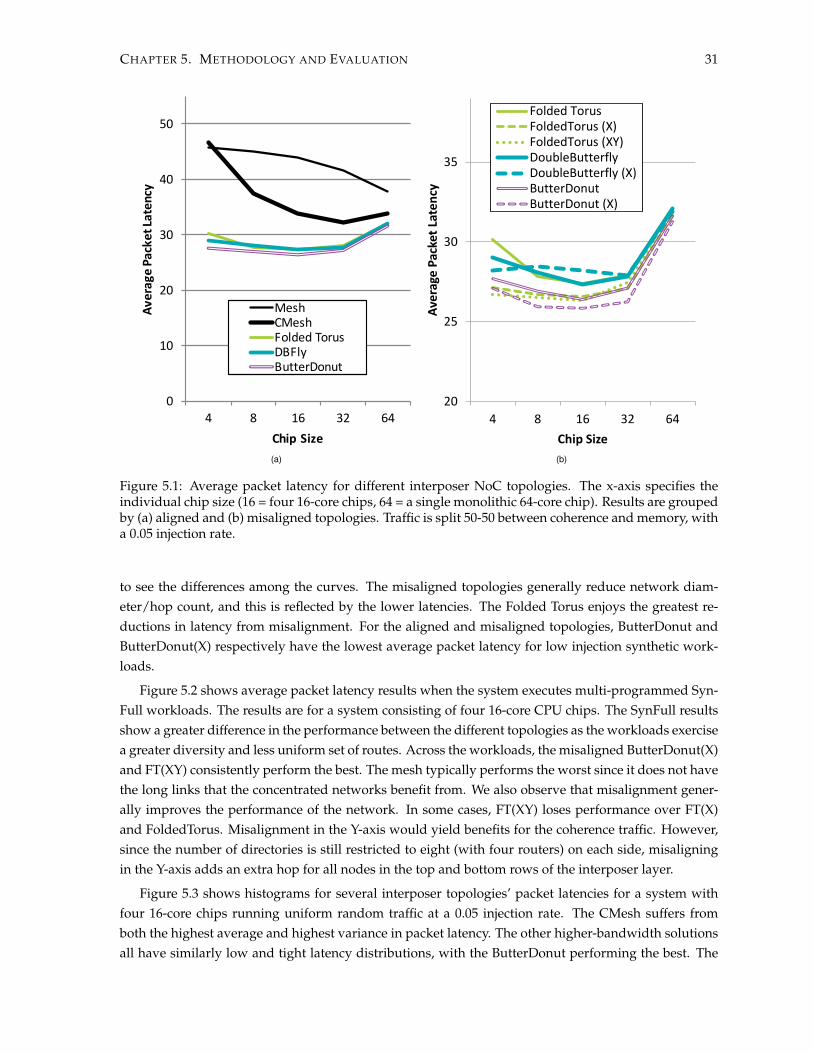
CHAPTER 5. METHODOLOGY AND EVALUATION 31
0
10
20
30
40
50
4 8 16 32 64
AveragePacketLa
tency
ChipSize
MeshCMeshFoldedTorusDBFlyButterDonut
20
25
30
35
4 8 16 32 64A
vera
ge P
acke
t La
ten
cyChip Size
Folded TorusFoldedTorus (X)FoldedTorus (XY)DoubleButterflyDoubleButterfly (X)ButterDonutButterDonut (X)
(a) (b)
Figure 5.1: Average packet latency for different interposer NoC topologies. The x-axis specifies theindividual chip size (16 = four 16-core chips, 64 = a single monolithic 64-core chip). Results are groupedby (a) aligned and (b) misaligned topologies. Traffic is split 50-50 between coherence and memory, witha 0.05 injection rate.
to see the differences among the curves. The misaligned topologies generally reduce network diam-eter/hop count, and this is reflected by the lower latencies. The Folded Torus enjoys the greatest re-ductions in latency from misalignment. For the aligned and misaligned topologies, ButterDonut andButterDonut(X) respectively have the lowest average packet latency for low injection synthetic work-loads.
Figure 5.2 shows average packet latency results when the system executes multi-programmed Syn-Full workloads. The results are for a system consisting of four 16-core CPU chips. The SynFull resultsshow a greater difference in the performance between the different topologies as the workloads exercisea greater diversity and less uniform set of routes. Across the workloads, the misaligned ButterDonut(X)and FT(XY) consistently perform the best. The mesh typically performs the worst since it does not havethe long links that the concentrated networks benefit from. We also observe that misalignment gener-ally improves the performance of the network. In some cases, FT(XY) loses performance over FT(X)and FoldedTorus. Misalignment in the Y-axis would yield benefits for the coherence traffic. However,since the number of directories is still restricted to eight (with four routers) on each side, misaligningin the Y-axis adds an extra hop for all nodes in the top and bottom rows of the interposer layer.
Figure 5.3 shows histograms for several interposer topologies’ packet latencies for a system withfour 16-core chips running uniform random traffic at a 0.05 injection rate. The CMesh suffers fromboth the highest average and highest variance in packet latency. The other higher-bandwidth solutionsall have similarly low and tight latency distributions, with the ButterDonut performing the best. The

CHAPTER 5. METHODOLOGY AND EVALUATION 32
0
10
20
30
40
50
60
70
L-L-L-LAVG M-M-L-LAVG M-M-M-MAVG H-H-L-LAVG H-H-M-MAVG
AveragePacketLa
tency
MeshCMeshFoldedTorusFoldedTorus(X)FoldedTorus(XY)ButterDonutButterDonut (X)
Figure 5.2: Average packet latency results for different multi-programmed SynFull workloads, witheach benchmark denoted by the combination of the groups they are derived from (based on averageaccepted injection rate)
0.00
0.05
0.10
0.15
0.20
0.25
0.30
0.35
0.40
10 15 20 25 30 35 40 45 50 >50Frac
tio
n o
f al
l Pac
kets
Latency
CMesh
FoldedTorus
FoldedTorus (XY)
DoubleButterfly (X)
ButterDonut (X)
Figure 5.3: Distribution of message latencies (0.05 injection rate)
low average hop counts of these NoCs keep average latency down, and the higher bandwidth reducespathological traffic jams that would otherwise result in longer tails in the distributions.
Figure 5.4 shows the full-system results for several PARSEC [7] benchmarks (with the simmediumdataset) normalized to a mesh interposer network. These results are consistent with the network latencyresults in Figure 5.1. For workloads with limited network or memory pressure, many topologies exhibitsimilar network latencies which results in little full-system performance variation across topologies.
The primary characteristics of each of the benchmarks we evaluated is shown in Table 5.3. Blacksc-holes has a small working set and little data sharing or exchange. The various threads, once they begin,are largely independent of one another. Due to this, blackscholes puts limited pressure on the mem-ory system and the network and therefore sees little difference across topologies. Bodytrack is also adata-parallel model and puts a little more pressure on the network. We observe a little more variationacross the topologies. We also notice a slightly larger improvement over the baseline (interposer meshnetwork). Canneal has an unstructured parallel-programming model. It performs cache-aware simu-lated annealing. An important aspect of canneal is that it makes use of an aggressive synchronizationstrategy. It promotes data race recovery instead of avoidance [8]. As such, it makes very little use of

CHAPTER 5. METHODOLOGY AND EVALUATION 33
0
0.2
0.4
0.6
0.8
1
1.2
1.4
blackscholes bodytrack canneal dedup ferret x264
Norm
alize
dRu
ntim
eCMeshFoldedTorusFoldedTorus (X)FoldedTorus (XY)ButterDonutButterDonut(X)
Figure 5.4: Normalized runtime (To Mesh Interposer Network) for full-system simulation with a four16-core chips
Model Granularity Sharing Exchangeblackscholes FinancialAnalysis data-parallel coarse small low lowbodyrack ComputerVision data-parallel medium medium high mediumcanneal Engineering unstructured fine unbounded high highdedup EnterpiseStorage pipeline medium unbounded high highferret SimilaritySearch pipeline medium unbounded high highx264 MediaProcessing pipeline coarse medium high high
DataUsageWorkingSetApplication ApplicationDomain
Parallelization
Table 5.3: Characteristics of the PARSEC benchmarks used in this study [8]
locks or barriers. Thus, we see around 10% improvement over the baseline when using concentrationbut little variability across the different topology. Dedup, ferret, and x264 are more memory intensiveworkloads. These kernels have a pipelined programming model to parallelize the application. Theyalso have high data sharing and exchange and a large number of locks and waits (on condition vari-ables) [8]. Due to this, we see large improvements with the FoldedTorus and the ButterDonut. We alsosee that misalignment improves the system performance in many cases. In some cases, we notice aperformance drop (which we did not observe with synthetic workloads or SynFull workloads). This islikely due to the way we allocated the threads for the full-system applications. Since we started allocat-ing threads from the north-west corner, the master thread inevitably gets allocated to the corner node.Misalignment, on general, improves performance but has a negative effect on some nodes (includingthe nodes on the edge, especially the ones on the corner). We believe that we would see improvedperformance with a random or a smart thread-to-core allocation mechanism.
5.2.2 Load vs. Latency Analysis
The SynFull simulations hint at the impact of network load on the performance of the NoC. BecauseSynFull is designed to mimic the actual injection rates and patterns of real applications, it is difficult

CHAPTER 5. METHODOLOGY AND EVALUATION 34
0
10
20
30
40
50
0.01
0.02
0.03
0.04
0.05
0.06
0.07
0.08
0.09
0.10
0.11
0.12
AveragePa
cketLa
tency
InjectionRate
MeshCMeshFoldedTorusDoubleButterflyButterDonut
0
10
20
30
40
50
0.01
0.02
0.03
0.04
0.05
0.06
0.07
0.08
0.09
0.10
0.11
0.12
AveragePa
cketLa
tency
InjectionRate
FoldedTorusFoldedTorus(X)FoldedTorus(XY)DoubleButterflyDoubleButterfly(X)ButterDonutButterDonut(X)
(a) (b)
Figure 5.5: Latency and saturation throughput for (a) conventional NoC topologies and (b) misalignedtopologies.
to use it to arbitrarily sweep a range of traffic loads. To generate latency-load plots, we revert backto synthetic uniform random traffic (50-50 coherence and memory). We evaluate a system with four16-core chips. Figure 5.5(a) and (b) show the latency-load curves for the same topologies shown earlierin Figure 5.1. For the aligned topologies, the CMesh quickly saturates as its four links crossing thebisection of the chip quickly become a bottleneck. The remaining topologies maintain consistently lowlatencies up until they hit saturation. The misaligned topologies generally follow the same trends,although FT(XY) shows a substantially higher saturation bandwidth. The reason is that the Butterfly-derived topologies are optimized for east-west traffic to route memory traffic, and as a result are slightlyimbalanced. Looking back at Figure 4.7, ButterDonut has 12 links across the east-west bisection, butonly eight links going across the north-south cut. FT(XY) on the other hand has ten links across bothbisections, and scales out better. The cost (see Table 4.1) is that FT(XY) has 25% more router nodes and39% more links than ButterDonut, which can impact the yield of the minimally-active interposer.
Figure 5.6 further breaks down the load-latency curves into (a) memory traffic only, and (b) cachecoherence traffic only. The results are fairly similar across the two traffic types, with the memory traffichaving a slightly larger spread in average latencies due to the higher diversity in path lengths (memoryrequests always have to travel farther to the edges). The plots come from the same set of experiments,and therefore the saturation onset occurs at the same point in both graphs.
In general, from standard topologies to their misaligned variants, latency decreases and saturationthroughput improves. Saturation throughput improvements come from taking pressure off of the east-west bisection links in the aligned topologies. Latency reductions come from shorter hop counts inthese networks.
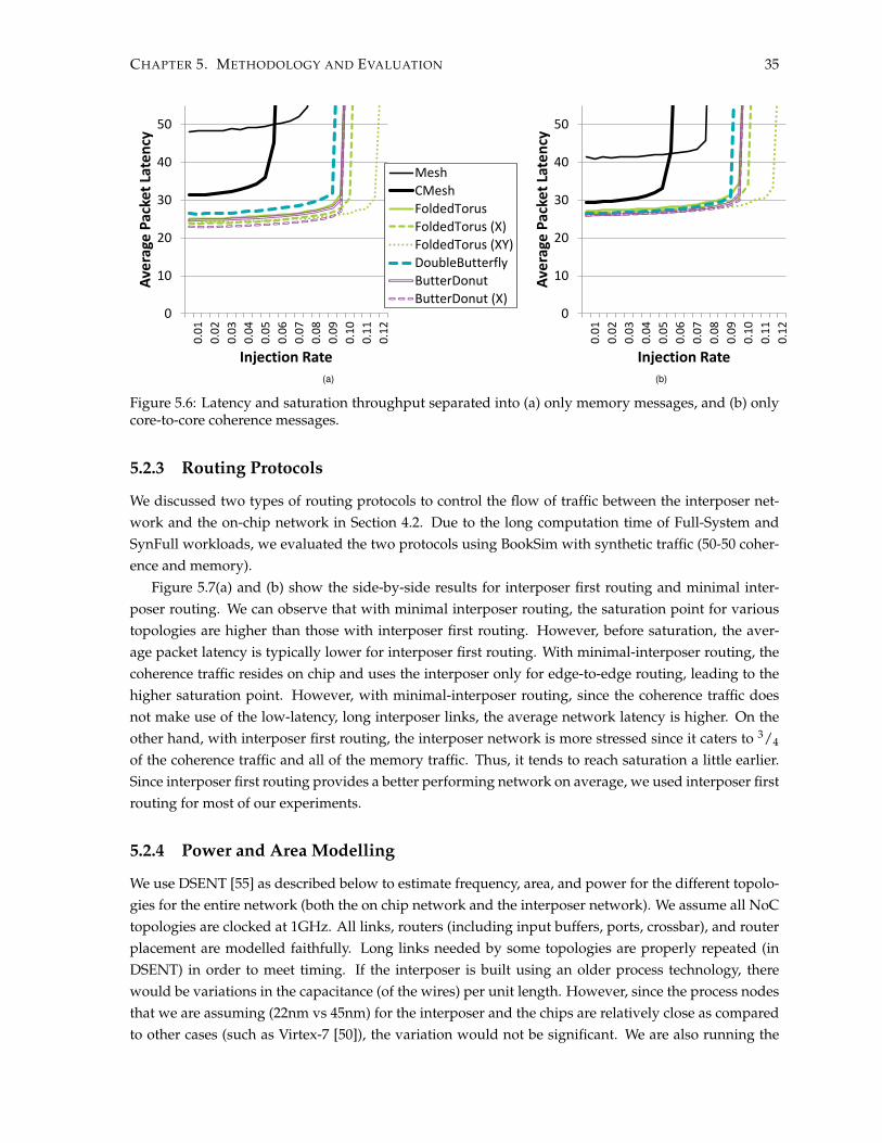
CHAPTER 5. METHODOLOGY AND EVALUATION 35
0
10
20
30
40
50
0.0
1
0.0
2
0.0
3
0.0
4
0.0
5
0.0
6
0.0
7
0.0
8
0.0
9
0.1
0
0.1
1
0.1
2
Ave
rage
Pac
ket
Late
ncy
Injection Rate
Mesh
CMesh
FoldedTorus
FoldedTorus (X)
FoldedTorus (XY)
DoubleButterfly
ButterDonut
ButterDonut (X)0
10
20
30
40
50
0.01
0.02
0.03
0.04
0.05
0.06
0.07
0.08
0.09
0.10
0.11
0.12
Ave
rage
Pac
ket
Late
ncy
Injection Rate (a) (b)
Figure 5.6: Latency and saturation throughput separated into (a) only memory messages, and (b) onlycore-to-core coherence messages.
5.2.3 Routing Protocols
We discussed two types of routing protocols to control the flow of traffic between the interposer net-work and the on-chip network in Section 4.2. Due to the long computation time of Full-System andSynFull workloads, we evaluated the two protocols using BookSim with synthetic traffic (50-50 coher-ence and memory).
Figure 5.7(a) and (b) show the side-by-side results for interposer first routing and minimal inter-poser routing. We can observe that with minimal interposer routing, the saturation point for varioustopologies are higher than those with interposer first routing. However, before saturation, the aver-age packet latency is typically lower for interposer first routing. With minimal-interposer routing, thecoherence traffic resides on chip and uses the interposer only for edge-to-edge routing, leading to thehigher saturation point. However, with minimal-interposer routing, since the coherence traffic doesnot make use of the low-latency, long interposer links, the average network latency is higher. On theother hand, with interposer first routing, the interposer network is more stressed since it caters to 3/4
of the coherence traffic and all of the memory traffic. Thus, it tends to reach saturation a little earlier.Since interposer first routing provides a better performing network on average, we used interposer firstrouting for most of our experiments.
5.2.4 Power and Area Modelling
We use DSENT [55] as described below to estimate frequency, area, and power for the different topolo-gies for the entire network (both the on chip network and the interposer network). We assume all NoCtopologies are clocked at 1GHz. All links, routers (including input buffers, ports, crossbar), and routerplacement are modelled faithfully. Long links needed by some topologies are properly repeated (inDSENT) in order to meet timing. If the interposer is built using an older process technology, therewould be variations in the capacitance (of the wires) per unit length. However, since the process nodesthat we are assuming (22nm vs 45nm) for the interposer and the chips are relatively close as comparedto other cases (such as Virtex-7 [50]), the variation would not be significant. We are also running the
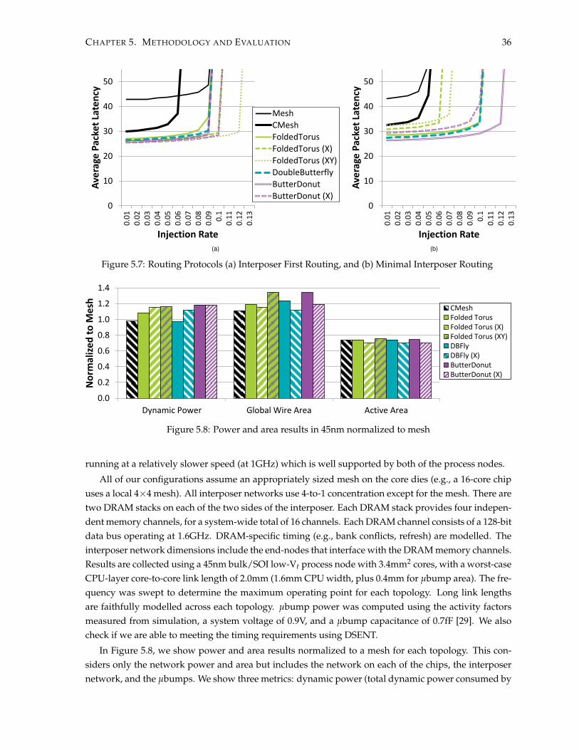
CHAPTER 5. METHODOLOGY AND EVALUATION 36
0
10
20
30
40
50
0.0
10
.02
0.0
30
.04
0.0
50
.06
0.0
70
.08
0.0
90
.10
.11
0.1
20
.13
Ave
rage
Pac
ket
Late
ncy
Injection Rate
Mesh
CMesh
FoldedTorus
FoldedTorus (X)
FoldedTorus (XY)
DoubleButterfly
ButterDonut
ButterDonut (X)0
10
20
30
40
50
0.01
0.02
0.03
0.04
0.05
0.06
0.07
0.08
0.09
0.1
0.11
0.12
0.13
Ave
rage
Pac
ket
Late
ncy
Injection Rate(a) (b)
Figure 5.7: Routing Protocols (a) Interposer First Routing, and (b) Minimal Interposer Routing
0.0
0.2
0.4
0.6
0.8
1.0
1.2
1.4
Dynamic Power Global Wire Area Active Area
No
rmal
ize
d t
o M
esh
CMeshFolded TorusFolded Torus (X)Folded Torus (XY)DBFlyDBFly (X)ButterDonutButterDonut (X)
Figure 5.8: Power and area results in 45nm normalized to mesh
running at a relatively slower speed (at 1GHz) which is well supported by both of the process nodes.
All of our configurations assume an appropriately sized mesh on the core dies (e.g., a 16-core chipuses a local 4×4 mesh). All interposer networks use 4-to-1 concentration except for the mesh. There aretwo DRAM stacks on each of the two sides of the interposer. Each DRAM stack provides four indepen-dent memory channels, for a system-wide total of 16 channels. Each DRAM channel consists of a 128-bitdata bus operating at 1.6GHz. DRAM-specific timing (e.g., bank conflicts, refresh) are modelled. Theinterposer network dimensions include the end-nodes that interface with the DRAM memory channels.Results are collected using a 45nm bulk/SOI low-Vt process node with 3.4mm2 cores, with a worst-caseCPU-layer core-to-core link length of 2.0mm (1.6mm CPU width, plus 0.4mm for µbump area). The fre-quency was swept to determine the maximum operating point for each topology. Long link lengthsare faithfully modelled across each topology. µbump power was computed using the activity factorsmeasured from simulation, a system voltage of 0.9V, and a µbump capacitance of 0.7fF [29]. We alsocheck if we are able to meeting the timing requirements using DSENT.
In Figure 5.8, we show power and area results normalized to a mesh for each topology. This con-siders only the network power and area but includes the network on each of the chips, the interposernetwork, and the µbumps. We show three metrics: dynamic power (total dynamic power consumed by
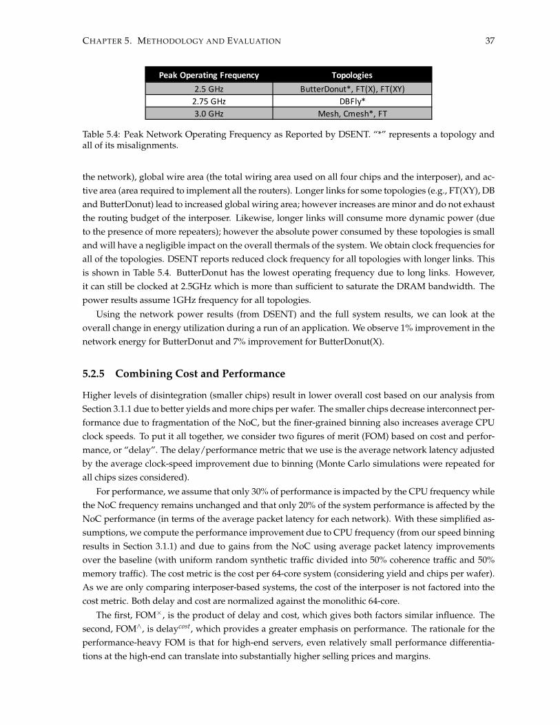
CHAPTER 5. METHODOLOGY AND EVALUATION 37
PeakOperatingFrequency Topologies2.5GHz ButterDonut*,FT(X),FT(XY)2.75GHz DBFly*3.0GHz Mesh,Cmesh*,FT
Table 5.4: Peak Network Operating Frequency as Reported by DSENT. “*” represents a topology andall of its misalignments.
the network), global wire area (the total wiring area used on all four chips and the interposer), and ac-tive area (area required to implement all the routers). Longer links for some topologies (e.g., FT(XY), DBand ButterDonut) lead to increased global wiring area; however increases are minor and do not exhaustthe routing budget of the interposer. Likewise, longer links will consume more dynamic power (dueto the presence of more repeaters); however the absolute power consumed by these topologies is smalland will have a negligible impact on the overall thermals of the system. We obtain clock frequencies forall of the topologies. DSENT reports reduced clock frequency for all topologies with longer links. Thisis shown in Table 5.4. ButterDonut has the lowest operating frequency due to long links. However,it can still be clocked at 2.5GHz which is more than sufficient to saturate the DRAM bandwidth. Thepower results assume 1GHz frequency for all topologies.
Using the network power results (from DSENT) and the full system results, we can look at theoverall change in energy utilization during a run of an application. We observe 1% improvement in thenetwork energy for ButterDonut and 7% improvement for ButterDonut(X).
5.2.5 Combining Cost and Performance
Higher levels of disintegration (smaller chips) result in lower overall cost based on our analysis fromSection 3.1.1 due to better yields and more chips per wafer. The smaller chips decrease interconnect per-formance due to fragmentation of the NoC, but the finer-grained binning also increases average CPUclock speeds. To put it all together, we consider two figures of merit (FOM) based on cost and perfor-mance, or “delay”. The delay/performance metric that we use is the average network latency adjustedby the average clock-speed improvement due to binning (Monte Carlo simulations were repeated forall chips sizes considered).
For performance, we assume that only 30% of performance is impacted by the CPU frequency whilethe NoC frequency remains unchanged and that only 20% of the system performance is affected by theNoC performance (in terms of the average packet latency for each network). With these simplified as-sumptions, we compute the performance improvement due to CPU frequency (from our speed binningresults in Section 3.1.1) and due to gains from the NoC using average packet latency improvementsover the baseline (with uniform random synthetic traffic divided into 50% coherence traffic and 50%memory traffic). The cost metric is the cost per 64-core system (considering yield and chips per wafer).As we are only comparing interposer-based systems, the cost of the interposer is not factored into thecost metric. Both delay and cost are normalized against the monolithic 64-core.
The first, FOM×, is the product of delay and cost, which gives both factors similar influence. Thesecond, FOM∧, is delaycost, which provides a greater emphasis on performance. The rationale for theperformance-heavy FOM is that for high-end servers, even relatively small performance differentia-tions at the high-end can translate into substantially higher selling prices and margins.
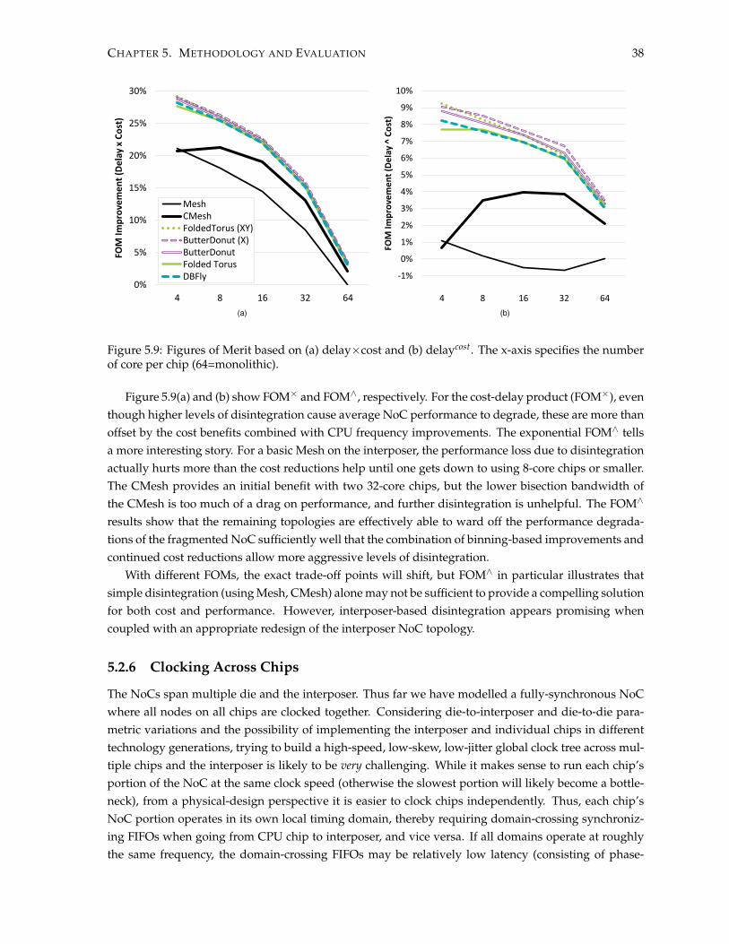
CHAPTER 5. METHODOLOGY AND EVALUATION 38
0%
5%
10%
15%
20%
25%
30%
4 8 16 32 64
FOM
Imp
rove
me
nt
(De
lay
x C
ost
)
MeshCMeshFoldedTorus (XY)ButterDonut (X)ButterDonutFolded TorusDBFly -1%
0%
1%
2%
3%
4%
5%
6%
7%
8%
9%
10%
4 8 16 32 64
FOM
Imp
rove
me
nt
(De
lay
^ C
ost
)
(a) (b)
Figure 5.9: Figures of Merit based on (a) delay×cost and (b) delaycost. The x-axis specifies the numberof core per chip (64=monolithic).
Figure 5.9(a) and (b) show FOM× and FOM∧, respectively. For the cost-delay product (FOM×), eventhough higher levels of disintegration cause average NoC performance to degrade, these are more thanoffset by the cost benefits combined with CPU frequency improvements. The exponential FOM∧ tellsa more interesting story. For a basic Mesh on the interposer, the performance loss due to disintegrationactually hurts more than the cost reductions help until one gets down to using 8-core chips or smaller.The CMesh provides an initial benefit with two 32-core chips, but the lower bisection bandwidth ofthe CMesh is too much of a drag on performance, and further disintegration is unhelpful. The FOM∧
results show that the remaining topologies are effectively able to ward off the performance degrada-tions of the fragmented NoC sufficiently well that the combination of binning-based improvements andcontinued cost reductions allow more aggressive levels of disintegration.
With different FOMs, the exact trade-off points will shift, but FOM∧ in particular illustrates thatsimple disintegration (using Mesh, CMesh) alone may not be sufficient to provide a compelling solutionfor both cost and performance. However, interposer-based disintegration appears promising whencoupled with an appropriate redesign of the interposer NoC topology.
5.2.6 Clocking Across Chips
The NoCs span multiple die and the interposer. Thus far we have modelled a fully-synchronous NoCwhere all nodes on all chips are clocked together. Considering die-to-interposer and die-to-die para-metric variations and the possibility of implementing the interposer and individual chips in differenttechnology generations, trying to build a high-speed, low-skew, low-jitter global clock tree across mul-tiple chips and the interposer is likely to be very challenging. While it makes sense to run each chip’sportion of the NoC at the same clock speed (otherwise the slowest portion will likely become a bottle-neck), from a physical-design perspective it is easier to clock chips independently. Thus, each chip’sNoC portion operates in its own local timing domain, thereby requiring domain-crossing synchroniz-ing FIFOs when going from CPU chip to interposer, and vice versa. If all domains operate at roughlythe same frequency, the domain-crossing FIFOs may be relatively low latency (consisting of phase-
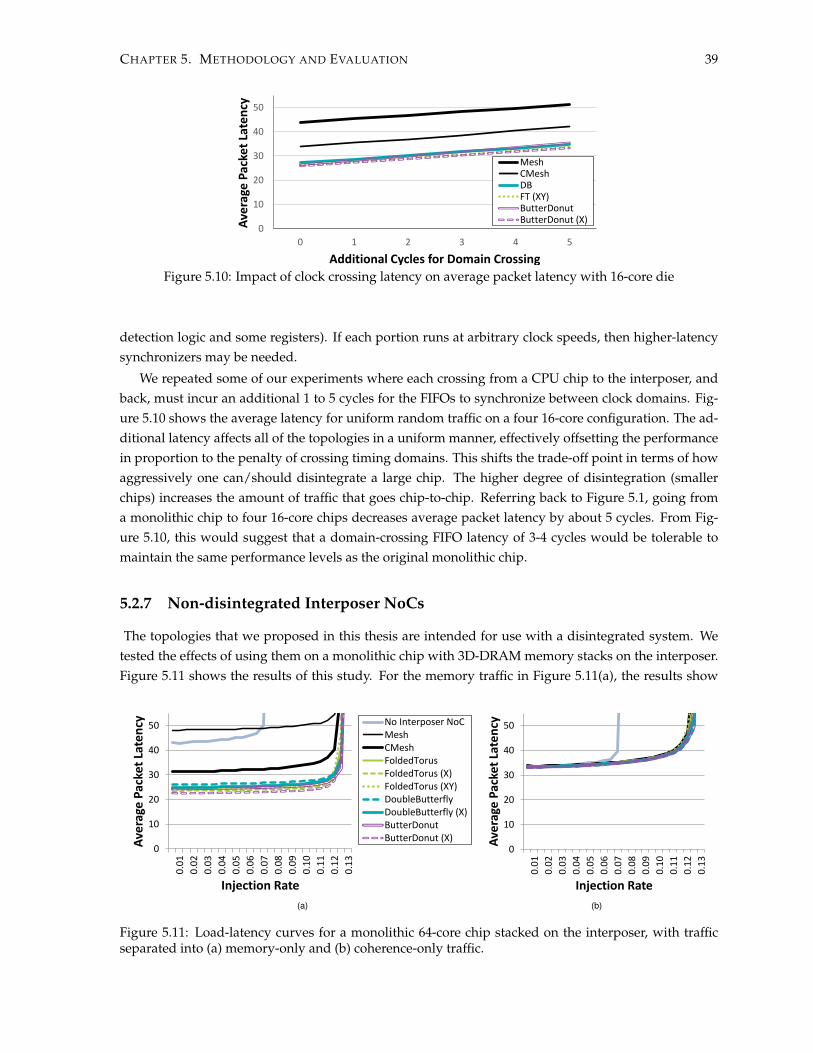
CHAPTER 5. METHODOLOGY AND EVALUATION 39
0
10
20
30
40
50
0 1 2 3 4 5A
vera
ge P
acke
t La
ten
cyAdditional Cycles for Domain Crossing
MeshCMeshDBFT (XY)ButterDonutButterDonut (X)
Figure 5.10: Impact of clock crossing latency on average packet latency with 16-core die
detection logic and some registers). If each portion runs at arbitrary clock speeds, then higher-latencysynchronizers may be needed.
We repeated some of our experiments where each crossing from a CPU chip to the interposer, andback, must incur an additional 1 to 5 cycles for the FIFOs to synchronize between clock domains. Fig-ure 5.10 shows the average latency for uniform random traffic on a four 16-core configuration. The ad-ditional latency affects all of the topologies in a uniform manner, effectively offsetting the performancein proportion to the penalty of crossing timing domains. This shifts the trade-off point in terms of howaggressively one can/should disintegrate a large chip. The higher degree of disintegration (smallerchips) increases the amount of traffic that goes chip-to-chip. Referring back to Figure 5.1, going froma monolithic chip to four 16-core chips decreases average packet latency by about 5 cycles. From Fig-ure 5.10, this would suggest that a domain-crossing FIFO latency of 3-4 cycles would be tolerable tomaintain the same performance levels as the original monolithic chip.
5.2.7 Non-disintegrated Interposer NoCs
The topologies that we proposed in this thesis are intended for use with a disintegrated system. Wetested the effects of using them on a monolithic chip with 3D-DRAM memory stacks on the interposer.Figure 5.11 shows the results of this study. For the memory traffic in Figure 5.11(a), the results show
0
10
20
30
40
50
0.0
1
0.0
2
0.0
3
0.0
4
0.0
5
0.0
6
0.0
7
0.0
8
0.0
9
0.1
0
0.1
1
0.1
2
0.1
3
Ave
rage
Pac
ket
Late
ncy
Injection Rate
No Interposer NoCMeshCMeshFoldedTorusFoldedTorus (X)FoldedTorus (XY)DoubleButterflyDoubleButterfly (X)ButterDonutButterDonut (X)
0
10
20
30
40
50
0.01
0.02
0.03
0.04
0.05
0.06
0.07
0.08
0.09
0.10
0.11
0.12
0.13
Ave
rage
Pac
ket
Late
ncy
Injection Rate
(a) (b)
Figure 5.11: Load-latency curves for a monolithic 64-core chip stacked on the interposer, with trafficseparated into (a) memory-only and (b) coherence-only traffic.

CHAPTER 5. METHODOLOGY AND EVALUATION 40
that our new approach of misaligned topologies improves upon the prior topologies even for a non-disintegrated system. Our best performing topology, ButterDonut(X), provides a ∼9% improvement inaverage packet latency over the best prior topology (the aligned DB). Optimizing NoC designs for aninterposer-based monolithic SoC was not the goal of our work, but the additional improvements are awelcome result.
Summary
In this chapter, we described the methodology we used to evaluate our designs in terms of power, area,frequency, and performance. We used DSENT for power, area, and frequency analysis. For power,we evaluated our designs using three different methods; we used synthetic traffic workloads, SynFullworkloads, and full-system simulations. Between these three types of workloads, we cover a diverseset of test-cases. We include an analysis, comparing two different types of routing protocols and studythe effects of clock jitter between the different clocking domains of the interposer network and the on-chip network We also compared our multi-chip design to a monolithic design. Effectively, we show thebenefits of our proposed designs as well as highlight a few of the disadvantages. In the next chapter,we qualitatively compare our proposed design with other recent works.
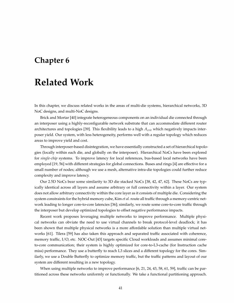
Chapter 6
Related Work
In this chapter, we discuss related works in the areas of multi-die systems, hierarchical networks, 3DNoC designs, and multi-NoC designs.
Brick and Mortar [40] integrate heterogeneous components on an individual die connected throughan interposer using a highly-reconfigurable network substrate that can accommodate different routerarchitectures and topologies [39]. This flexibility leads to a high Acrit which negatively impacts inter-poser yield. Our system, with less heterogeneity, performs well with a regular topology which reducesareas to improve yield and cost.
Through interposer-based disintegration, we have essentially constructed a set of hierarchical topolo-gies (locally within each die, and globally on the interposer). Hierarchical NoCs have been exploredfor single-chip systems. To improve latency for local references, bus-based local networks have beenemployed [19, 56] with different strategies for global connections. Buses and rings [4] are effective for asmall number of nodes; although we use a mesh, alternative intra-die topologies could further reducecomplexity and improve latency.
Our 2.5D NoCs bear some similarity to 3D die stacked NoCs [38, 42, 47, 62]. These NoCs are typ-ically identical across all layers and assume arbitrary or full connectivity within a layer. Our systemdoes not allow arbitrary connectivity within the core layer as it consists of multiple die. Considering thesystem constraints for the hybrid memory cube, Kim et al. route all traffic through a memory-centric net-work leading to longer core-to-core latencies [36]; similarly, we route some core-to-core traffic throughthe interposer but develop optimized topologies to offset negative performance impacts.
Recent work proposes leveraging multiple networks to improve performance. Multiple physi-cal networks can obviate the need to use virtual channels to break protocol-level deadlock; it hasbeen shown that multiple physical networks is a more affordable solution than multiple virtual net-works [61]. Tilera [59] has also taken this approach and separated traffic associated with coherence,memory traffic, I/O, etc. NOC-Out [43] targets specific Cloud workloads and assumes minimal core-to-core communication; their system is highly optimized for core-to-L3-cache (for Instruction cachemiss) performance. They use a butterfly to reach L3 slices and a different topology for the cores. Sim-ilarly, we use a Double Butterfly to optimize memory traffic, but the traffic patterns and layout of oursystem are different resulting in a new topology.
When using multiple networks to improve performance [6, 21, 24, 43, 58, 61, 59], traffic can be par-titioned across these networks uniformly or functionally. We take a functional partitioning approach.
41

CHAPTER 6. RELATED WORK 42
However, the presence of the interposer makes a large difference: memory traffic uses the interposer,while core traffic stays on the local core mesh. Additionally, due to the presence of multiple separate diefor our cores, our partitioning is not strict (some core traffic must use the interposer network to reachremote cores).

Chapter 7
Future Directions & Conclusions
7.1 Future Directions
The presence of two networks (on-chip and interposer) allows for a variety of designs that we have notexplored in this work. For the on-chip network, we used a standard mesh network. Using differenttypes of networks (including those with concentration) could be a good way to improve coherencetraffic on chip. Multiple networks are often used to improve performance. We could potentially usemultiple networks on the interposer to improve the performance: we could use prioritization schemessuch as [20] or [52] or we could separate different types of traffic at the physical layer (more affordablethan using multiple virtual networks [61].
7.1.1 New Chip-design Concerns
This work assumes the disintegration of a multi-core chip into smaller die, with the implicit assump-tion that all die are identical. This creates a new physical design and layout challenge as each diemust implement a symmetric interface; for example, a given die could be placed on the left side ofthe interposer or the right, and that same exact die must correctly interface with the interposer regard-less of its mounting position. Conventional SoCs have no such requirements for their layouts. Thisextends beyond functional interfaces, to issues such as power delivery (the power supply must be reli-able independent of chip placement) and thermal management (temperature may vary depending onchip location). Many of these challenges are more in the domain of physical design and EDA/CADtool optimization, but we mention it here to paint a fair picture of some of the other challenges forinterposer-based disintegration.
7.1.2 Software-based Mitigation of Multi-Chip Interposer Effects
Disintegration introduces additional challenges and opportunities for optimization at the softwarelevel. With a monolithic 64-core NoC, there is already non-uniformity in latency between varioussource-destination pairs as hop count increases, which is exacerbated in a disintegrated system. Care-ful scheduling to place communicating threads on the same chips could reduce chip-to-chip traffic andalleviate congestion on the interposer. Similarly, careful data-allocation to place frequently used datain the 3D stacks close to the threads that use the data can minimize memory latency and cut down on
43

CHAPTER 7. FUTURE DIRECTIONS & CONCLUSIONS 44
cross-interposer traffic. Coordinating scheduling decisions to simultaneously optimize for both coher-ence and memory traffic could provide further benefits but would require support from the operatingsystem. While we believe there are many interesting opportunities to involve the software layers tohelp mitigate the impacts of a multi-chip NoC organization, we leave it for future research.
7.2 Conclusion
In this work, we looked at a conventional baseline 2.5D multi-core system. We made the key insightthat if the chip is already using a silicon interposer for integration of multiple chips, any additionalresources used on the interposer (provided that timing is met) are essentially “free”. We can then usethese resources to either add more computational logic or routing. These resources can be used todesign new network topologies as well as integrate multiple chips on a single interposer die.
We propose disintegrating a large monolithic chip into multiple smaller chips. We then integratethe smaller chips on an interposer to replicate the functionality of the larger chip. We do an exten-sive cost versus performance study of this approach, considering the various trade-offs including area,power, yield, network latency, system performance, and chip speeds. We then design and evaluate NoCtopologies for 2.5D architectures. One of our key contributions here is the introduction of “misaligned”concentrated network topologies. These topologies specifically cater to cross-chip communication andshow good promise for multi-chip systems. We demonstrate that our designs can significantly improveperformance over the baseline mesh network. We show that even when under peak use in our sys-tem, the active area (router logic) can be reduced around 30% when using concentration while reapingperformance benefits. There is an increase in the global wire area (by 10-30%) as well as increase indynamic power but the overall energy can be reduced by 7%. It is important to note that this extrawiring comes from the interposer metal layers which was previously unused. Our proposal is able tooffer a method to integrate large chips while maintaining (and in cases, improving) performance. Bydoing so, we may be able to manufacture larger chips than possible on a monolithic design.
Ultimately, we show that instead of using a monolithic chip on a 2.5D interposer system, it isfavourable (in terms of energy, area, and performance) to disintegrate the large chip into multiplesmaller chips and use an underlying NoC on the interposer to replicate the original function.

Bibliography
[1] AMD Corp. High Bandwidth Memory (HBM). http://www.amd.com/Documents/High-Bandwidth-Memory-HBM.pdf.
[2] William Dally and. B. Towles. Principles and Practices of Interconnection Networks. Morgan Kauf-mann, 2003.
[3] Krit Athikulwongse, Ashutosh Chakraborty, Jae-Sok Yang, David Z. Pan, and Sung Kyu Lim.Stress-Driven 3D-IC Placement with TSV Keep-Out Zone and Regularity Study. In Intl. Conf. onComputer-Aided Design, pages 669–674, San Jose, CA, November 2010.
[4] Rachata Ausavarungnirun, Chris Fallin, Xiangyao Yu, Kevin Change, Greg Nazario, ReetuparnaDas, Gabriel Loh, and Onur Mutlu. Design and evaluation of hierarchical rings with deflectionrouting. In Proceedings of the International Symposium on Computer Architecture and High PerformanceComputing, 2014.
[5] Mario Badr and Natalie Enright Jerger. SynFull: Synthetic traffic models capturing a full range ofcache coherence behaviour. In Intl. Symp. on Computer Architecture, June 2014.
[6] J. Balfour and W. J. Dally. Design tradeoffs for tiled CMP on-chip networks. In Intl. Conf. onSupercomputing, 2006.
[7] Christian Bienia. Benchmarking Modern Multiprocessors. PhD thesis, Princeton University, January2011.
[8] Christian Bienia, Sanjeev Kumar, Jaswinder Pal Singh, and Kai Li. The parsec benchmark suite:Characterization and architectural implications. In Proceedings of the 17th international conference onParallel architectures and compilation techniques, pages 72–81. ACM, 2008.
[9] Nathan Binkert, Bradford Beckmann, Gabriel Black, Steven K. Reinhardt, Ali Saidi, ArkapravaBasu, Joel Hestness, Derek R. Hower, Tushar Krishna, Somayeh Sardashti, Rathijit Sen, KoreySewell, Muhammad Shoaib, Nilay Vaish, Mark D. Hill, and David A. Wood. gem5: A Multiple-ISA Full System Simulator with Detailed Memory Model. Computer Architecture News, 39, June2011.
[10] Bryan Black. Die Stacking is Happening. In Intl. Symp. on Microarchitecture, Davis, CA, December2013.
[11] Eric Bogatin, Dick Potter, and Laura Peters. Roadmaps of packaging technology. Integrated CircuitEngineering Scottsdale, 1997.
[12] Mark Bohr. A 30 year retrospective on dennard’s mosfet scaling paper. Solid-State Circuits SocietyNewsletter, IEEE, 12(1):11–13, 2007.
[13] Mark T Bohr et al. Interconnect scaling-the real limiter to high performance ulsi. In InternationalElectron Devices Meeting, pages 241–244. INSTITUTE OF ELECTRICAL & ELECTRONIC ENGI-NEERS, INC (IEEE), 1995.
[14] Shekhar Borkar. Design challenges of technology scaling. Micro, IEEE, 19(4):23–29, 1999.
45

BIBLIOGRAPHY 46
[15] Lizhong Chen and Timothy M. Pinkston. Worm-bubble flow control. In 19th Intl. Symp. on HighPerformance Computer Architecture, 2013.
[16] Chung-Kuan Cheng. Breaking the Wall of Interconnect: Research and Education. http://cseweb.ucsd.edu/~kuan/talk/interconnect.ppt.
[17] Jason Cong and Yan Zhang. Thermal-Driven Multilevel Routing for 3-D ICs. In 10th Asia SouthPacific Design Automation Conference, Shanghai, China, January 2005.
[18] William J Dally and Brian Towles. Route packets, not wires: On-chip interconnection networks. InDesign Automation Conference, 2001. Proceedings, pages 684–689. IEEE, 2001.
[19] Reetuparna Das, Soumya Eachempati, Asit K. Mishra, Vijaykrishnan Narayanan, and Chita R.Das. Design and evaluation of a hierarchical on-chip interconnect for next-generation cmps. InIntl. Symp. on High Performance Computer Architecture, 2009.
[20] Reetuparna Das, Onur Mutlu, Thomas Moscibroda, and Chita R Das. Aérgia: exploiting packetlatency slack in on-chip networks. In ACM SIGARCH computer architecture news, volume 38, pages106–116. ACM, 2010.
[21] Reetuparna Das, Satish Narayanasamy, Sudhir K. Satpathy, and Ronald Dreslinski. Catnap: En-ergy proportional multiple network-on-chip. In Intl. Symp. on Computer Architecture, 2013.
[22] Yangdong Deng and Wojciech Maly. Interconnect Characteristics of 2.5-D System IntegrationScheme. In Intl. Symp. on Physical Design, pages 171–175, Sonoma County, CA, April 2001.
[23] Robert H Dennard, VL Rideout, E Bassous, and AR Leblanc. Design of ion-implanted mosfet’swith very small physical dimensions. Solid-State Circuits, IEEE Journal of, 9(5):256–268, 1974.
[24] Natalie Enright Jerger, Ajaykumar Kannan, Zimo Li, and Gabriel H. Loh. NoC architectures forsilicon interposer systems. In 47th Intl. Symp. on Microarchitecture, pages 458–470, Cambridge, UK,December 2014.
[25] Michael Hackerott. Die Per Wafer Calculator. Informatic Solutions, LLC, 2011.
[26] Jen-Hsun Huang. NVidia GPU Technology Conference: Keynote. Technical report, March 2013.
[27] Ron Huemoeller. Through Silicon Via (TSV) Product Technology. Technical report, Amkor Tech-nology, February 2012. Presented to IMAPS North Carolina Chapter.
[28] Wei-Lun Hung, Greg Link, Yuan Xie, Narayanan Vijaykrishnan, and Mary Jane Irwin. Interconnectand Thermal-aware Floorplanning for 3D Microprocessors. In 7th Intl. Symp. on Quality ElectronicDesign, San Jose, CA, March 2006.
[29] Institute of Microelectronics. Process Design Kit (PDF) for 2.5D Through Silicon Interposer (TSI)Design Enablement & 2.5D TSI Cost Modeling, August 2012.
[30] An Intel. Introduction to the intel quickpath interconnect. White Paper, 2009.
[31] Michael Jackson. A Silicon Interposer-based 2.5D-IC Design Flow, Going 3D by Evolution Ratherthan by Revolution. Technical report, Synopsis Insight Newsletter, 2012. Issue 1.
[32] JEDEC. High Bandwidth Memory (HBM) DRAM. http://www.jedec.org/standards-documents/docs/jesd235.
[33] JEDEC. Wide I/O Single Data Rate (Wide I/O SDR). http://www.jedec.org/standards-documents/docs/jesd229.
[34] Nan Jiang, Daniel U. Becker, George Michelogiannakis, James Balfour, Brian Towles, John Kim,and William J. Dally. A detailed and flexible cycle-accurate network-on-chip simulator. InIntl. Symp. on Performance Analysis of Systems and Software, 2013.

BIBLIOGRAPHY 47
[35] Ajaykumar Kannan, Natalie Enright Jerger, and Gabriel H. Loh. Enabling interposer-based disin-tegration of multi-core processors. In 48th Intl. Symp. on Microarchitecture, Hawaii, US, December2015.
[36] G. Kim, J. Kim, J-H. Ahn, and J. Kim. Memory-centric system interconnect design with hybridmemory cubes. In Intl. Conf. on Parallel Architectures and Compilation Techniques, 2013.
[37] J-S. Kim, C. Oh, H. Lee, D. Lee, H-R. Hwang, S. Hwang, B. Na, J. Moon, J-G. Kim, H. Park, J-W.Ryu, K. Park, S-K. Kang, S-Y. Kim, H. Kim, J-M. Bang, H. Cho, M. Jang, C. Han, J-B. Lee, K. Kyung,J-S. Choi, and Y-H. Jun. A 1.2V 12.8GB/s 2Gb Mobile Wide-I/O DRAM with 4x128 I/Os UsingTSV-Based Stacking. In ISSCC, 2011.
[38] Jongman Kim, Chrysostomos Nicopoulos, Dongkook Park, Reetuparna Das, Yuan Xie, N. Vijaykr-ishnan, Mazin S. Yousif, and Chita R. Das. A Novel Dimensionally-Decomposed Router for On-Chip Communication in 3D Architectures. In 34th Intl. Symp. on Computer Architecture, San Diego,CA, June 2007.
[39] M. Mercaldi Kim, J. D. Davis, M. Oskin, and T. Austin. Polymorphic on-chip networks. InIntl. Symp. on Computer Architecture, 2008.
[40] M. Mercaldi Kim, M. Mehrara, M. Oskin, and T. Austin. Architectural implications of brick andmortar silicon manufacturing. In Intl. Symp. on Computer Architecture, 2007.
[41] Dong Uk Lee, Kyung Whan Kim, Kwan Weon Kim, Hongjung Kim, Ju Young Kim, Young JunPark, Jae Hwan Kim, Dae Suk Kim, Heat Bit Park, Jin Wook Shin, et al. 25.2 a 1.2 v 8gb 8-channel128gb/s high-bandwidth memory (hbm) stacked dram with effective microbump i/o test methodsusing 29nm process and tsv. In Solid-State Circuits Conference Digest of Technical Papers (ISSCC), 2014IEEE International, pages 432–433. IEEE, 2014.
[42] Feihui Li, Chrysostomos Nicopoulos, Thomas Richardson, Yuan Xie, Vijaykrishnan Narayanan,and Mahmut Kandemir. Design and Management of 3D Chip Multiprocessors Using Network-in-Memory. In 33rd Intl. Symp. on Computer Architecture, pages 130–141, Boston, MA, June 2006.
[43] Pejman Lotfi-Kamran, Boris Grot, and Babak Falsafi. NOC-Out: Microarchitecting a Scale-OutProcessor. In Intl. Symp. on Microarchitecture, pages 177–187, Vancouver, BC, December 2012.
[44] Sheng Ma, Zhiying Wang, Zonglin Liu, and Natalie Enright Jerger. Leaving one slot empty: Flitbubble flow control for torus cache-coherent NoCs. IEEE Transactions on Computers, 64:763–777,March 2015.
[45] Mike O’Connor. Highlights of the High-Bandwidth Memory (HBM) Standard. In Memory ForumWorkshop, June 2014.
[46] C. Okoro, M. Gonzalez, B. Vandevelde, B. Swinnen, G. Eneman, S. Stoukatch, E. Beyne, and D. Van-depitte. Analysis of the Induced Stresses in Silicon During Thermocompression Cu-Cu Bondingof Cu-Through-Vias in 3D-SIC Architecture. In the Electronic Components and Technology Conference,pages 249–255, Reno, NV, May 2007.
[47] Dongkook Park, Soumya Eachempati, Reetuparna Das, Asit K. Mishra, Yuan Xie, Narayana Vi-jaykrishnan, and Chita R. Das. MIRA: A Multi-layered On-chip Interconnect Router Architecture.In Intl. Symp. on Computer Architecture, pages 251–261, Beijing, China, June 2008.
[48] V. Puente, C. Izu, R. Beivide, J. A. Gregorio, F. Vallejo, and J. M. Prellezo. The adaptive bubblerouter. Journal of Parallel and Distributed Computing, 64(9):1180–1208, 2001.
[49] Kiran Puttaswamy and Gabriel H. Loh. Thermal Analysis of a 3D Die-Stacked High-PerformanceMicroprocessor. In ACM Great Lakes Symp. on VLSI, pages 19–24, Philadelphia, PA, May 2006.
[50] Kirk Saban. Xilinx Stacked Silicon Interconnect Technology Delivers Breakthrough FPGA Capac-ity, Bandwidth, and Power Efficiency. White paper, Xilinx, 2011. WP380 (v1.1).
BIBLIOGRAPHY 48
[51] T Sakurai and K Tamaru. Simple formulas for two- and three-dimensional capacitances. IEEETransactions on Electron Devices, 30(2):183–185, 1983.
[52] Joshua San Miguel and Natalie Enright Jerger. Data criticality in network-on-chip design. 2015.
[53] Mike Santarini. Stacked & Loaded: Xilinx SSI, 28-Gbps I/O Yield Amazing FPGAs. Technicalreport, Xilinx Xcell Journal, First Quarter 2011.
[54] C. H. Stapper. The Effects of Wafer to Wafer Defect Density Variations on Integrated Circuit Defectand Fault Distributions. IBM Journal of Research and Development, 29:87–97, January 1985.
[55] Chen Sun, Chia-Hsin Owen Chen, George Kurian, Lan Wei, Jason Miller, Anant Agarwal, Li-Shiuan Peh, and Vladimir Stojanovic. DSENT - a tool connecting emerging photonics with elec-tronics for opto-electronic networks-on-chip modeling. In NOCS, May 2012.
[56] Aniruddha N. Udipi, Naveen Muralimanohar, and Rajeev Balasubramonian. Towards scalable,energy-efficient, bus-based on-chip networks. In Intl. Symp. on High Performance Computer Archi-tecture, 2010.
[57] University of Texas. 65nm Wire Capacitance and Resistance Calculator. http://users.ece.utexas.edu/~mcdermot/vlsi-2/Wire_Capacitance_and_Resistance_65nm.xls.
[58] Stavros Volos, Ciprian Seiculescu, Boris Grot, Naser Khosro Pour, Babak Falsafi, and Giovanni DeMicheli. CCNoC: Specializing On-Chip Interconnects for Energy Efficiency in Cache CoherentServers. In 6th NOCS, pages 67–74, Lyngby, Denmark, May 2012.
[59] D. Wentzlaff, P. Griffin, H. Hoffmann, Liewei Bao, B. Edwards, C. Ramey, M. Mattina, Chyi-ChangMiao, J.F. Brown, and A. Agarwal. On-chip interconnection architecture of the Tile Processor.Micro, IEEE, 27(5):15 –31, Sept.-Oct. 2007.
[60] Yuan Xie, Gabriel H. Loh, Bryan Black, and Kerry Bernstein. Design Space Exploration for 3DArchitecture. ACM Journal of Emerging Technologies in Computer Systems, 2(2):65–103, April 2006.
[61] Y. J. Yoon, N. Concer, M. Petracca, and L. Carloni. Virtual channels vs. multiple physical networks:a comparative analysis. In Design Automation Conference, 2010.
[62] Aamir Zia, Sachhidh Kannan, Garret Rose, and H. Jonathan Chao. Highly-scalable 3D Clos NoCfor Many-core CMPs. In NEWCAS Conference, pages 229–232, Montreal, Canada, June 2010.


![Pemetaan Kannan[1]](https://static.fdocuments.net/doc/165x107/5695d50b1a28ab9b02a3cdb4/pemetaan-kannan1.jpg)