
Bulk Nanostructured FCC Steels With Enhanced … Reports/814 Final Report for... · Project No....
156
Project No. 09-814 Bulk Nanostructured FCC Steels With Enhanced Radiation Tolerance F lC l R&D Fuel Cycle R&D Dr. Xinghang Zhang Texas A&M University In collaboration with: Ui i f Wi i M di University of Wisconsin‐Madison Texas A&M University University of Florida Los Alamos National Laboratory Argonne National Laboratory Stu Maloy, Technical POC Sue Lesica, Federal POC
Transcript of Bulk Nanostructured FCC Steels With Enhanced … Reports/814 Final Report for... · Project No....
Project No. 09-814
Bulk Nanostructured FCC Steels With Enhanced Radiation Tolerance
F l C l R&DFuel Cycle R&D
Dr. Xinghang Zhang
Texas A&M University
In collaboration with:
U i i f Wi i M diUniversity of Wisconsin‐Madison
Texas A&M University
University of Florida
Los Alamos National Laboratory
Argonne National Laboratory
Stu Maloy, Technical POCSue Lesica, Federal POC

Annual Progress Report October 27, 2012 DE-AC07-05ID14517
1
FINAL PROGRESS REPORT
Project title: Bulk nanostructured austenitic stainless steels with enhanced radiation tolerance
Covering period: Oct. 1, 2009 through Sep. 30, 2012
Date of Report: October 27, 2012
Recipient: Texas Engineering Experiment Station
Address: Texas Engineering Experiment Station
TEES Research Services
006 WERC, Mail Stop 3406 TAMU
College Station, TX 77843-3406
Tel: 979-845-1264
Fax: 979-845-9643
URL: trsweb.tamu.edu
Award Number: DE-AC07-05ID14517
Project Number (Subcontract no.): 00088120
Subcontractors: University of Wisconsin, Madison; University of Florida
Other Partners: Dr. Stuart Maloy, Email: [email protected], Los Alamos National Laboratory
Contact(s):
Principal Investigator: Xinghang Zhang, 979-845-2143 (O), [email protected]
Co-PI: K. Ted Hartwig, 979-845-1585 (O), [email protected]
Co-PI: Todd Allen, 608-265-4083 (O), [email protected]
Co-PI: Yong Yang, 352-846-3791 (O) [email protected]
Annual Progress Report October 27, 2012 DE-AC07-05ID14517
2
1. Project Objective
The objective of this project is to increase radiation tolerance in austenitic steels through
optimization of grain size and grain boundary (GB) characteristics. The focus will be on
nanocrystalline austenitic Fe-Cr-Ni alloys with an fcc crystal structure. The long-term goal is to
design and develop bulk nanostructured austenitic steels with enhanced void swelling resistance
and substantial ductility, and to enhance their creep resistance at elevated temperatures via GB
engineering. The combination of grain refinement and grain boundary engineering approaches
allows us to tailor the material strength, ductility, and resistance to swelling by 1) changing the
sink strength for point defects, 2) by increasing the nucleation barriers for bubble formation at
GBs, and 3) by changing the precipitate distributions at boundaries.
Compared to ferritic/martensitic steels, austenitic stainless steels (SS) possess good creep
and fatigue resistance at elevated temperatures, and better toughness at low temperature.
However, a major disadvantage of austenitic SS is that they are vulnerable to significant void
swelling in nuclear reactors, especially at the temperatures and doses anticipated in the Advanced
Burner Reactor. The lack of resistance to void swelling in austenitic alloys led to the switch to
ferritic/martensitic steels as the preferred material for the fast reactor cladding application.
Recently a type of austenitic stainless steel, HT-UPS, was developed at ORNL, and is expected
to show enhanced void swelling resistance through the trapping of point defects at nanometer-
sized carbides. Reducing the grain size and increasing the fraction of low energy grain
boundaries should reduce the available radiation-produced point defects (due to the increased
sink area of the grain boundaries), should make bubble nucleation at the boundaries less likely
(by reducing the fraction of high-energy boundaries), and improve the strength and ductility
under radiation by producing a higher density of nanometer sized carbides on the boundaries.
This project will focus on void swelling but advances in processing of austenitic steels are likely
to also improve the radiation response of the mechanical properties.
2. Brief summary of major accomplishment - milestones
This is a very fruitful project. In collaboration with Dr. Jinsung Jang (KAERI, South
Korea), we have made the following major progress.

Annual Progress Report October 27, 2012 DE-AC07-05ID14517
3
(1) We examined the deformation mechanisms in ECAPed Fe-14Cr-16Ni alloys. The average
grain size has been refined from 700 microns down to ~ 400 nanometers. The yield strength of
ECAP alloys is 5-6 times greater than coarse-grained alloys, and the ductility remain very high,
~ 15% uniform elongation. What is more, these ultra fine grained alloys retain strong work
hardening capacity. This is rare as most ECAPed alloys have very little work hardening
capability. The strain rate sensitivity of the alloys is lower than bulk alloys.
(2) Ex situ isothermal annealing experiments showed the fine microstructure was thermally
stable up to 673 K, and abnormal grain growth occurred at ~ 873 K. In situ annealing studies in a
transmission electron microscope revealed the coarsening of grains. Analysis of grain growth
kinetics from 873 to 1073 K yielded activation energy of grain growth to be ~ 207 kJ/mol. The
grain growth mechanisms and annealing induced evolution of mechanical properties were
discussed.
(3) He ion irradiation resistance of ultra fine grained Fe-14Cr-16Ni alloys. At a peak fluence
level of 5.5 displacement per atom (dpa), helium bubbles, 0.5-2 nm in diameter, were observed
in both coarse-grained (CG) and ultrafine grained (UFG) alloy. The density of He bubbles,
dislocation loops, as well as radiation hardening were significantly reduced in the UFG Fe-Cr-Ni
alloy comparing to those in its CG counterpart. The results imply that radiation tolerance in bulk
metals can be effectively enhanced by refinement of microstructures.
(4) Significant microstructural damage, in the form of defect clusters, typically occurs in metals
subjected to heavy ion irradiation. High angle grain boundaries have long been postulated as
sinks for defect clusters, such as dislocation loops. Here we provide direct evidence, via in situ
Kr ion irradiation under a transmission electron microscope, that high angle grain boundaries in
nanocrystalline Ni, with an average grain size of ~ 55 nm, can effectively absorb radiation
induced dislocation loops. These high angle grain boundaries significantly reduce the density and
size of radiation induced dislocation loops in nanocrystalline Ni compared to their bulk
counterparts, and thus nanocrystalline Ni achieves significant enhancement of radiation tolerance.

Annual Progress Report October 27, 2012 DE-AC07-05ID14517
4
(5) Multiscale microstructure refinement of a 12Cr-ODS steel by equal channel angular extrusion
(ECAE) is investigated by numerous microscopy techniques. The as-HIPped material showed a
bimodal microstructure. Three types of second phase particles, including Y2O3, (Cr, Fe)23C6 and
Cr oxide, were observed. The orientation correlation between Y2O3 and the matrix were found to
be (020)α // (00 4
)Y2O3 and [001]α // [110]Y2O3. After ECAE, the large grains were refined and a
homogeneous grain size was achieved. The Cr rich phases (Cr oxide and Cr carbide) were
effectively refined. Yttrium oxide particles around the prior ultrafine grain boundaries were
redistributed. Geometry change of large yttrium oxide particles from round or facet to triangular
or elliptic shaped was observed. Hardening by ~ 35 % is hypothesized through the dislocation
pile-ups mechanism against grain boundaries.
(6) During the annealing of 12 Cr ODS steel, the core-shell structure of the oxide particles was
formed, which can be understood as the original growth of the Y2O3 particles where transition
chromium oxides were formed as a case of low oxygen content in the matrix.
(7) The microstructure feature, mechanical properties and their response to heat treatment of cold
ECAEed and hot ECAEed T91 alloys were studied. Cold ECAE was more effective in grain
refinement, while hot ECAE was more effective in particle refinement. The refining mechanism
of precipitates is due to the chemical elimination of prior austenite grain boundaries during hot
ECAE, where is a potential preference nucleation site for carbides.
(8) In situ Kr radiation was performed on ECAPed Fe-14Cr-16Ni alloys. Studies show that the
dislocation loop density in ECAPed alloys is much lower than that in coarse grained (as-
received) alloys. Furthermore, no defect denuded zone was observed along grain boundaries in
UFG specimens. This may be related to the fact that grain size (~ 400 nm) is greater than TEM
foil thickness (~ 100 nm), and thus foil surfaces act as defect sinks as well.
(9) DSC experiments show that the the ECAPed Fe-14Cr-16Ni alloys should be thermally stable
at a temperature below ~600C, the materials display a radiation induced growth behavior even
at the temperature as low as 300C possible due to the irradiation assisted grain boundary
migration and coalesce of subgrains from annihilation of dislocations (grains portioned by

Annual Progress Report October 27, 2012 DE-AC07-05ID14517
5
dislocation walls). Nevertheless, the processed materials demonstrate a good radiation swelling
resistance and no voids were observed up to a dose of 50 dpa.
(10) 304L and 316L stainless were processed by ECAP. The final products have an average grain
size of ~ 100nm and grains are mostly equiaxed. The microstructure and tensile behavior of these
alloys are studied. ECAP induces significant strengthening in these alloys.
(11) The microstructure and texture evolution of oxide dispersion strengthened ferritic steel
during stepwise uniaxial tensile deformation were observed by high-resolution electron
backscattered diffraction with a newly designed deformation device. The rotation behavior of
individual ferrite grains as well as overall preferred orientation were traced and analyzed. The
tendency describes that the grains rotate towards the stable orientation of 〈1 0 0〉//ND and
〈1 1 1〉//ND. The degree of rotation was dependent on their initial orientation. Vickers
hardness test and transmission electron microscope analysis were performed before and after
uniaxial tensile deformation to correlate the microstructure with its mechanical properties.
(12) Fe ion irradiation of ECAPed Fe-17Cr-12Ni-2.5Mo alloys indicated that the crystal
structure of irradiated sample surface has changed from FCC to BCC phase. The sizes of the
newly developed BCC grains were consistent with the ion irradiation depth, which could be
estimated by molecular dynamics simulations.
Project Organization:

Annual Progress Report October 27, 2012 DE-AC07-05ID14517
6
3. Project status - major progress
Major progress
Several projects have been running in parallel at each institution and through intimate
collaborations. As each project contains several tasks listed in the above schematics, it is natural
to group the projects based on their focus (rather tasks). For the sake of clarity, we summarized
below the major progress of 12 projects, each led by an institution with mutual collaborations.
Section A. US contribution
A1. Deformation mechanisms of ultrafine grained Fe-Cr-Ni alloy processed by ECAP
Lead organization (Texas A&M, Xinghang Zhang, K. Ted Hartwig)
In the previous annual report, we have presented preliminary studies on mechanical
properties of ECAPed Fe-Cr-Ni alloys. In this report, we present the complete studies of
deformation mechanisms in Fe-Cr-Ni alloys.
The material used in the ECAP experiments was Fe-14Cr-16Ni (wt.%) ternary alloy,
fabricated by vacuum cast and subsequent hot isostatic pressing, the initial average grain size is ~
700 µm. ECAP experiments were performed in a split die with channels intersecting at a contact
angle of 90°, which yield an effective strain of ~1.15 per single pass. The billet was machined to
be 19 × 19 × 152 mm, and eight passes ECAE were carried out on the sample at 500oC using
route Bc, which means that between subsequent passes, the sample was rotated by 90°
continuously around its longitudinal axes.
35 40 45 50 55 60 65 70 75 80
(220)
Inte
nsity
(a
.u.)
2
As-Received
As-Processed
(200)
(111)
(110)
Fig.1.1. XRD profile of the as-received CG and as-processed UFG Fe-Cr-Ni alloy. The as-received sample is fully austenitic, and there is a small α΄ (110) peak appears in the as-processed sample, which was taken from the longitudinal plane.
Annual Progress Report October 27, 2012 DE-AC07-05ID14517
7
Fig.1.1 shows the XRD profiles of as-received coarse grained (CG) and as-processed
ultra fine grained (UFG) Fe-Cr-Ni alloy. The as-received sample is fully austenitic. The as-
processed sample was taken from the longitudinal plane of the ECAPed billet. As shown in Fig.
1.1, a small α΄ (110) martensite peak appears. The peak intensity of austenite phase reduces and
the full width half maximum (FWHM) increases after ECAP experiments due to grain
refinement.
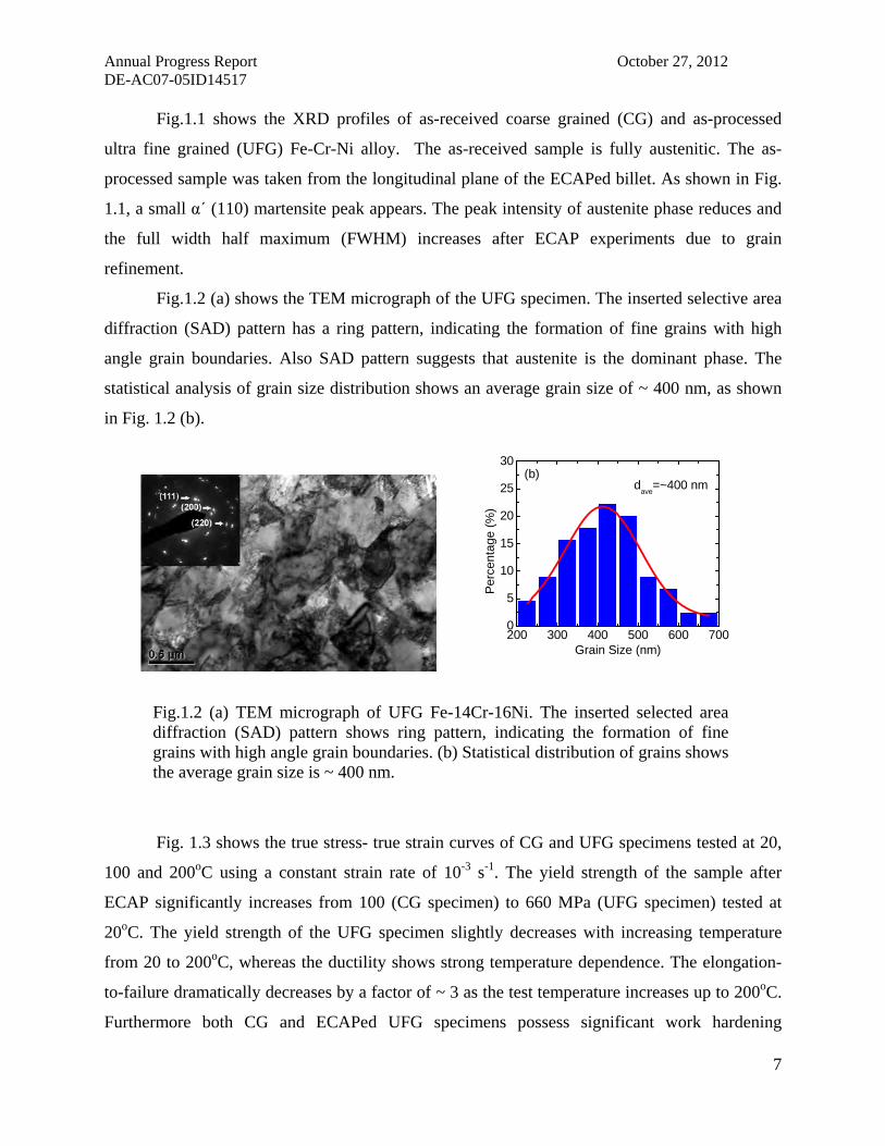
Fig.1.2 (a) shows the TEM micrograph of the UFG specimen. The inserted selective area
diffraction (SAD) pattern has a ring pattern, indicating the formation of fine grains with high
angle grain boundaries. Also SAD pattern suggests that austenite is the dominant phase. The
statistical analysis of grain size distribution shows an average grain size of ~ 400 nm, as shown
in Fig. 1.2 (b).
200 300 400 500 600 7000
5
10
15
20
25
30
Per
cent
age
(%)
Grain Size (nm)
dave
=~400 nm(b)
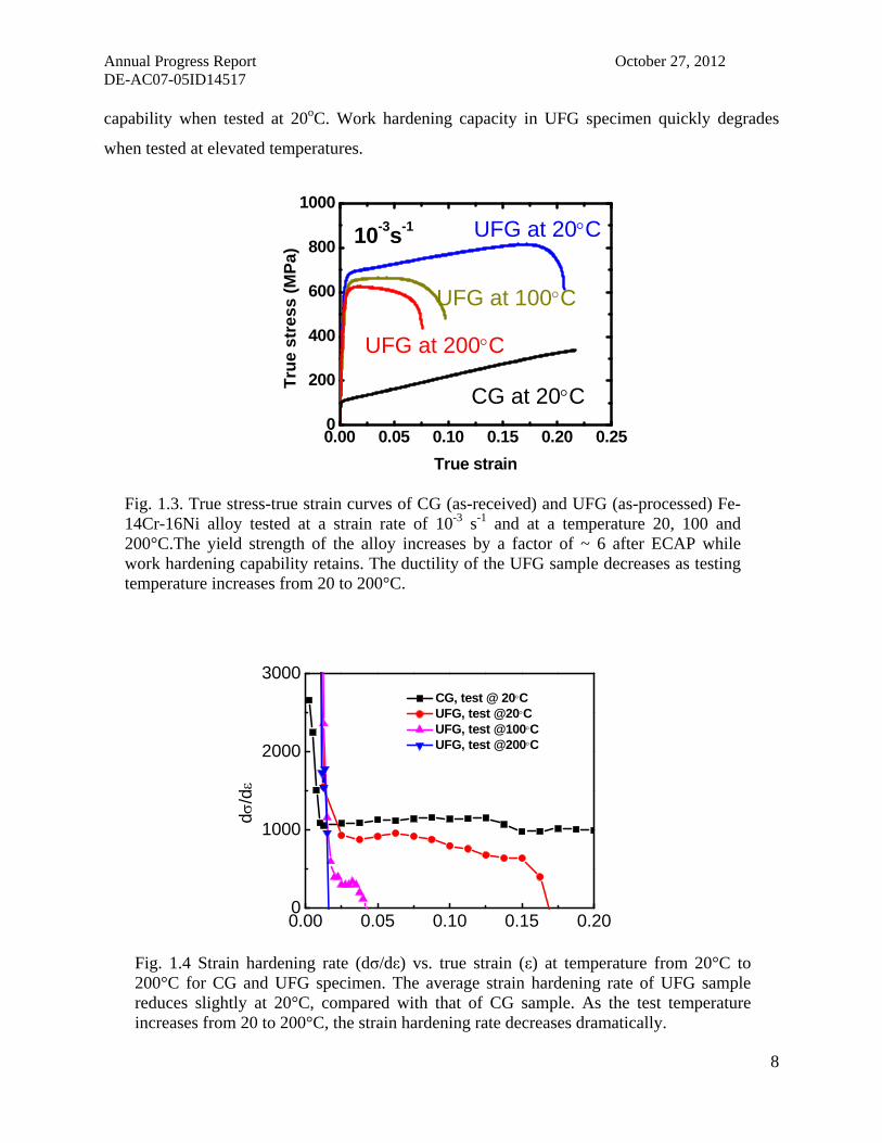
Fig. 1.3 shows the true stress- true strain curves of CG and UFG specimens tested at 20,
100 and 200oC using a constant strain rate of 10-3 s-1. The yield strength of the sample after
ECAP significantly increases from 100 (CG specimen) to 660 MPa (UFG specimen) tested at
20oC. The yield strength of the UFG specimen slightly decreases with increasing temperature
from 20 to 200oC, whereas the ductility shows strong temperature dependence. The elongation-
to-failure dramatically decreases by a factor of ~ 3 as the test temperature increases up to 200oC.
Furthermore both CG and ECAPed UFG specimens possess significant work hardening
Fig.1.2 (a) TEM micrograph of UFG Fe-14Cr-16Ni. The inserted selected area diffraction (SAD) pattern shows ring pattern, indicating the formation of fine grains with high angle grain boundaries. (b) Statistical distribution of grains shows the average grain size is ~ 400 nm.
Annual Progress Report October 27, 2012 DE-AC07-05ID14517
8
capability when tested at 20oC. Work hardening capacity in UFG specimen quickly degrades
when tested at elevated temperatures.
0.00 0.05 0.10 0.15 0.20 0.250
200
400
600
800
1000
10-3s-1
Tru
e s
tre
ss
(MP
a)
True strain
UFG at 20C
UFG at 100C
UFG at 200C
CG at 20C
0.00 0.05 0.10 0.15 0.200
1000
2000
3000 CG, test @ 20C UFG, test @20C UFG, test @100C UFG, test @200C
d/
d
Fig. 1.3. True stress-true strain curves of CG (as-received) and UFG (as-processed) Fe-14Cr-16Ni alloy tested at a strain rate of 10-3 s-1 and at a temperature 20, 100 and 200°C.The yield strength of the alloy increases by a factor of ~ 6 after ECAP while work hardening capability retains. The ductility of the UFG sample decreases as testing temperature increases from 20 to 200°C.
Fig. 1.4 Strain hardening rate (dσ/dε) vs. true strain (ε) at temperature from 20°C to 200°C for CG and UFG specimen. The average strain hardening rate of UFG sample reduces slightly at 20°C, compared with that of CG sample. As the test temperature increases from 20 to 200°C, the strain hardening rate decreases dramatically.

Annual Progress Report October 27, 2012 DE-AC07-05ID14517
9
Fig. 1.4 shows strain hardening rate (dσ/dε) as a function of a true strain (ε). Comparing
to CG specimen, the uniform strain hardening rate is slightly lower in UFG specimen tested at
20°C. As the testing temperature increases, the strain hardening rate of UFG specimen decreases
dramatically.
The SEM micrograph in Fig. 1.5 shows the fracture surface of the UFG specimen tested
at 20oC and 200°C. The dimple-like morphology dominates the fracture pattern after test
temperature of 20°C, implying that the failure mode is ductile rupture, while more area on
fracture surface tested at 200°C shows cleavage feature, as shown in Fig. 1.5 (b), although a few
dimples still can be observed.
Microstructure of the UFG sample after tensile test at 20°C was examined by TEM. As
shown in Fig. 1.6, the bright filed TEM image suggests that grains remain equiaxed, yet a higher
density of dislocations together with deformation twins are observed. The SAD pattern suggests
that austenite is still the dominant phase even though the samples were strained to a true strain of
more than 15%.
Fig. 1.5 (a) The fracture surface of UFG sample after testing at 20°C shows the dimple-like morphology. (b) The fracture surface of UFG sample subjected to the tensile test at 200°C shows dominated cleavage feature.

Annual Progress Report October 27, 2012 DE-AC07-05ID14517
10
Tensile jump tests at strain rates varying from 10-5 to 10-2 s-1 were performed to determine
the strain rate sensitivity. Fig. 1.7 (a) shows the jump test results of CG and UFG samples at
20°C. Fig. 1.7 (b) presents the jump test results for the UFG samples at 100 and 200°C up to ~
5% true strain. The numbers in Fig. 1.7 stand for the applied strain rates. For instance “-3”
represents a strain rate of 1 × 10⁻³ s-1.
0.00 0.03 0.06 0.09 0.12 0.15400
500
600
700
800
900
True strain
Tru
e st
ress
(M
Pa)
0
100
200
300
400
500
CG
True stress (M
Pa)
-3-2-3-4 -5 -4 -3UFG
-3-2-3-4 -5 -4 -3
0.00 0.01 0.02 0.03 0.04 0.05500
550
600
650
700
750
Tru
e S
tre
ss (
MP
a)
True Strain
100C
200C
-3-2 -3 -4 -5 -4 -3
-3-2 -3 -4 -5 -4 -3
UFG
Fig. 1.6. TEM micrograph of UFG specimen after tensile test at 20oC shows the retention of UFG grains with a few deformation twins. SAD pattern indicates the major phase remains austenite.
Fig. 1.7 (a) True stress-true strain curves of CG and UFG Fe-Cr-Ni alloy at 20°C, the strain rate varies between 10-5 s-1 to 10-2 s-1. (b) True stress-true strain curves of UFG specimen during jump tests at 100°C and 200°C in the first 5% plastic strain.

Annual Progress Report October 27, 2012 DE-AC07-05ID14517
11
The strain rate sensitivity exponent (m) can be calculated by
TTm ,, )log
)(1
()log
log(
(1),
where is true stress and is strain rate. The values of m can be calculated from the slope in the
plot of log vs. )log( , as shown in Fig. 1.8. At 20°C, the average value of m is estimated to be
~ 0.014 for CG specimen (the m value of bulk 304 SS at 30°C is ~ 0.012), By refining the gains,
the average m value of the UFG sample at 20°C is calculated to be ~ 0.007, and as test
temperature increases to 100 and 200°C, the m value rises to 0.009 and 0.012 respectively. The
relationship between strain rate sensitivity and activation volume v is
v
kTm
3
(2),
where k is Boltzmann constant. By using the slope of )log(3 kT vs. , we derive the activation
volume is ~ 130b3 (where b is the Burgers vector) for CG sample and ~ 38b3 for UFG sample at
20°C. At elevated temperature, the activation volume of the UFG specimen is reduced further to
be ~30b3 at 100°C and ~26b3 at 200°C.
-5 -4 -3 -21.9
2.0
2.8
2.9
log
()
(MP
a)
log()
CG @20C, m=0.0140.002
UFG @ 20C, m=0.0070.001
UFG @ 100C m=0.0090.002
UFG @200C, m=0.0120.001
Fig. 1.8 Plot of log(σ) vs. log( ), the strain rate sensitivity (m) is estimated by the slop of the curves. Average m value of CG and UFG specimen at 20C is calculated to be ~ 0.014 and ~ 0.007, respectively. For the UFG specimen, at elevated temperature, average value of m is ~ 0.009 at 100°C, and ~ 0.012 at 200°C.

Annual Progress Report October 27, 2012 DE-AC07-05ID14517
12
Strain hardening
The microstructure of Fe-Cr-Ni alloy is successfully refined by three orders of
magnitude, from 700 m for as-received material down to 400 nm by ECAP processing at
500oC. The microstructure refinement is achieved by continuous accumulation of dislocations
during severe plastic deformation. The increase of yield strength in UFG specimen at 20oC
mainly originates from the grain refinement. The contribution of martensite to hardening is
negligible as the predominant phase remains austenite after deformation. For most NC/UFG
metals and alloys produced by using severe plastic deformation (SPD), dislocation saturation is
achieved very quickly, resulting in the lack of strain hardening and diminished dislocation
activity during deformation. However, under hot working conditions, some NC/UFG metals and
alloys undergo dynamic recovery during SPD. The annihilation and rearrangement of
dislocations due to the dynamic recovery lower the average stain energy associated with the
dislocations and reduce the dislocation density inside the grains. The total dislocation density
evolution rate (
d
d) can be expressed as
d
d
d
d
d
d recostore (3),
where dstore/d stands for dislocation storage rate, which is an athermal component, and
dreco/d describes the dislocation density evolution due to dynamic recovery, which is
influenced by thermal activation. In this current study, the strain hardening rate of UFG
specimen at room temperature in the uniform deformation region is only slightly less than that of
CG specimen and the true uniform strain exceeds 15%. During ECAP processing at 500oC, the
dislocations produced by severe plastic deformation evolved into the grain boundaries and/or
annihilated by dislocations with opposite Burgers vector. Both processes lower the overall
dislocation density in grains. Dynamic recovery occurs during ECAP at elevated deformation
temperature, and consequently renders the UFG specimen strain hardening capacity when tested
at room temperature.
Annual Progress Report October 27, 2012 DE-AC07-05ID14517
13
The effect of dynamic recovery on strain hardening rate becomes stronger with increasing
temperature due to the increased mobility of dislocations. The strain hardening rate (
d
d) can be
described as
)],,([
Td
drh (4),
where h is an athermal hardening component due to dislocation storage, r is dynamic
recovery term related to the temperature, strain rate and flow stress. As shown in Fig.4, during
the uniaxial tensile tests, the strain hardening rate decreases quickly when temperature increases
to 200oC. It is likely dislocation density rapidly reduces through annihilation of dislocations or
grain boundary absorption. Both processes assist dynamic recovery and hence the strain
hardening rate is reduced. Although the strain hardening rate dramatically reduces when the
temperature rises to 200oC, the flow stresses only slight decreases. The retention of yield strength
at elevated temperature indicates that the equiaxed fine grains are thermally stable at the testing
temperature. The thermal stability of these UFG specimens will be reported elsewhere. The
moderate reduction of yield strength is a result of temperature assisted activation of dislocations
activities during the onset of plastic yielding.
Based on the Considere’s criterion, the plastic instability (necking) occurs when
)( (5)
where and are true stress and true strain, respectively. The rapid reduction of strain
hardening rate (
d
d) leads to the onset of necking at smaller strain, and thus reduces uniform
plastic strain during tensile tests.
Strain rate sensitivity of flow stress
The strain rate sensitivity of the Fe-Cr-Ni alloy reduces by a factor of 2 when the average
grain size is refined from 700 µm to 400 nm. Although the absolute flow stress increase per
strain rate of UFG specimen is larger than that of CG specimen, the m value still drops for the
smaller grain size due to the inversely proportional relationship with flow stress, in Eq.(1). A
Annual Progress Report October 27, 2012 DE-AC07-05ID14517
14
large activation volume estimated for CG specimen is related to the dislocations cutting through
the forest dislocations, while the reduced activation volume in UFG sample might be attributed
to the enhanced effect of grain boundary diffusion process. With the consideration of strain rate
sensitivity, the Hart’s instability criterion is
01)(1
md
d
(6),
It is clearly seen from the above equation that given the flow stress ( ), large strain
hardening rate (
d
d) and/or strain rate sensitivity (m) helps to sustain the homogeneous
deformation before the onset of necking. Although the average strain rate sensitivity of UFG
specimen increases from 0.007 to 0.012 by increasing the temperature from 20oC to 200oC, the
rapid drop of the strain hardening rate results in the reduction of uniform plastic strain at 200oC.
In other words, the strain rate sensitivity increase by temperature cannot compensate the decrease
of strain hardening rate, and the improvement of strain hardening would offer more resistance to
the onset of localized deformation.
A2. Thermal stability of ultra fine grains in ECAP processed Fe-14Cr-16Ni (wt.%) alloys
Lead organization (Texas A&M, Xinghang Zhang)
As-received Fe-14Cr-16Ni (wt.%) alloy had an average grain size of 700 µm. ECAP
experiments up to 8 passes at 773K were performed to refine its microstructure by using route
Bc, which means that between each subsequent pass, the sample was rotated by 90° around its
longitudinal axes. The grain boundary characteristics and phases identification of the ECAPed
sample were performed by using a LEO-1530 field emission scanning electron microscope
equipped with capability to perform electron backscattering diffraction (EBSD) analysis. Ex situ
annealing experiments were performed by using a vacuum furnace. The microstructure evolution
of the ECAPed specimen after annealing was examined with a Quanta 600 field emission
scanning electron microscope. In-situ annealing experiment was performed on a JEOL 2010
transmission electron microscope, operated at 200 kV and equipped with a Gatan SC1000
ORIUS CCD camera, at 973 K to study grain growth process. Samples for transmission electron

Annual Progress Report October 27, 2012 DE-AC07-05ID14517
15
microscopy (TEM) studies were prepared by electropolishing using a mixture of perchloric acid
and methanol solution. The microhardness of alloys was measured by using a Vickers
microhardness tester under a loading force of 200 gf for 13 seconds. The average hardness values
were determined from a minimum of 12 indentation experiments.
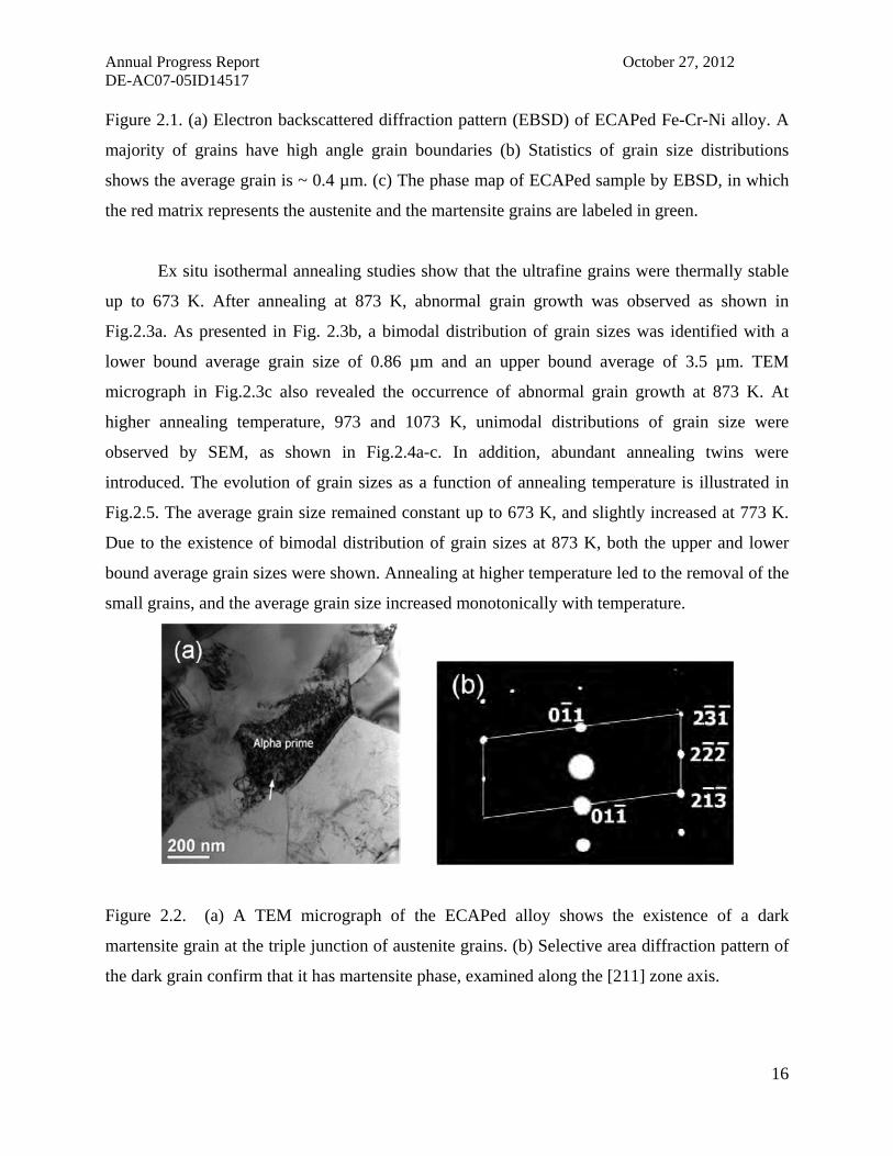
Fig.2.1 a shows the EBSD micrograph of ECAPed Fe-Cr-Ni alloy. The equiaxed
microstructure with high angle grain boundaries was formed after ECAP process. Statistics of
grain size distribution shown in Fig. 2.1b revealed an average grain size of ~ 0.4 µm. Fig.2.1c
shows the retention of predominant austenite matrix (red) with ~ 12% (area fraction) martensite
(green) dispersed along austenite grain boundaries. Martensite grains, as large as 0.3 µm, were
occasionally distributed at triple junctions of austenite grains. A TEM micrograph (Fig. 2.2a)
shows the existence of a large martensite grain at a triple junction of austenite grains. The
martensite phase appeared to have a very high density of dislocations and the inserted selected
area diffraction (SAD) pattern in Fig.2b confirmed the existence of α' martensite with body
centered cubic (bcc) structure oriented along [211] zone axis.
0.2 0.3 0.4 0.5 0.6 0.70.0
0.1
0.2
0.3
Num
ber
Fra
ctio
n
Grain size (m)
dave
=0.4m(b)
Annual Progress Report October 27, 2012 DE-AC07-05ID14517
16
Figure 2.1. (a) Electron backscattered diffraction pattern (EBSD) of ECAPed Fe-Cr-Ni alloy. A
majority of grains have high angle grain boundaries (b) Statistics of grain size distributions
shows the average grain is ~ 0.4 µm. (c) The phase map of ECAPed sample by EBSD, in which
the red matrix represents the austenite and the martensite grains are labeled in green.
Ex situ isothermal annealing studies show that the ultrafine grains were thermally stable
up to 673 K. After annealing at 873 K, abnormal grain growth was observed as shown in
Fig.2.3a. As presented in Fig. 2.3b, a bimodal distribution of grain sizes was identified with a
lower bound average grain size of 0.86 µm and an upper bound average of 3.5 µm. TEM
micrograph in Fig.2.3c also revealed the occurrence of abnormal grain growth at 873 K. At
higher annealing temperature, 973 and 1073 K, unimodal distributions of grain size were
observed by SEM, as shown in Fig.2.4a-c. In addition, abundant annealing twins were
introduced. The evolution of grain sizes as a function of annealing temperature is illustrated in
Fig.2.5. The average grain size remained constant up to 673 K, and slightly increased at 773 K.
Due to the existence of bimodal distribution of grain sizes at 873 K, both the upper and lower
bound average grain sizes were shown. Annealing at higher temperature led to the removal of the
small grains, and the average grain size increased monotonically with temperature.
Figure 2.2. (a) A TEM micrograph of the ECAPed alloy shows the existence of a dark
martensite grain at the triple junction of austenite grains. (b) Selective area diffraction pattern of
the dark grain confirm that it has martensite phase, examined along the [211] zone axis.

Annual Progress Report October 27, 2012 DE-AC07-05ID14517
17
0 1 2 3 4 5 6 7 8
0.0
0.1
0.2
0.3
0.4
Nu
mb
er F
ract
ion
Grain size (m)
upper bound,dave
=3.5m
lower bound, dave
=0.86m
(b) 873 K
Figure 2.3. (a) An SEM micrograph of UFG Fe-14Cr-16Ni after annealing at 873 K/1h shows
abnormal grain growth. (b) Statistics of grain sizes shows a bimodal distribution. The average
grain size of lower bound and upper bound is 0.86 and 3.5 µm respectively. (c) A TEM
micrograph of the alloy annealed at the same condition also shows the coexistence of small and
large grains.
2 3 4 5 6 7 8 9 100.0
0.1
0.2
0.3
0.4
Num
ber
Fra
ctio
n
Grain size (m)
(b) 973 Kd
ave=5.5 m
4 6 8 10 12 140.0
0.1
0.2
0.3
0.4
Nu
mbe
r F
ract
ion
Grain size (m)
dave
=8.4m(d) 1073 K

Annual Progress Report October 27, 2012 DE-AC07-05ID14517
18
Figure 2.4. (a) An SEM micrograph of UFG Fe-14Cr-16Ni after annealing at 973 K/1h shows
normal grain growth. Annealing twins were observed within grain. (b) Statistics of grain sizes of
the alloy annealed at 973K shows unimodal distribution with an average grain size of ~5.5 µm.
(c) An SEM micrograph of the alloy annealed at 1073 K/1h shows continuous grain growth and
the generation of annealing twins. (d) Corresponding grain size distribution is again unimodal
with an average grain size of ~ 8.4 µm.
273 473 673 873 10730
2
4
6
8
10
12
Gra
in s
ize
(m
)
Temperature (K)
upper bound
lower bound
Figure 2.6. The microstructure evolution of UFG sample subjected to in situ annealing at 973 K
inside a transmission electron microscope for various time. (a) At the onset of annealing. Five
grains are labeled as a - e. (b) Annealing for 5 minutes leads to the coalescence of grains a and b,
and c and d. Notice that grain e remains but becomes smaller. (c) After annealing for 10 minutes,
the morphology of grain e changes by presumably grain rotation.
Figure 2.5. Grain size evolution upon annealing shows that grains are rather stable up to 773 K, followed by rapid grain growth thereafter. Both the upper and lower bound average grain size are shown at 873 K, at which abnormal grain growth was observed.

Annual Progress Report October 27, 2012 DE-AC07-05ID14517
19
Microstructure evolution and grain growth in the UFG Fe-Cr-Ni alloy were observed by
in situ annealing in a transmission electron microscope. Fig.2.6 shows the bright field TEM
micrographs of the sample captured during annealing at 973 K for 0, 5, and 10 minutes. The
microstructure was manifested by several notable features. (a) At the beginning of annealing
studies, subgrains grew via rapid migration of grain boundaries, as evidenced by the coalescence
of subgrains labeled as a-d. (b) Meanwhile large grains grew by consuming small grains, which
is considered as the Ostwald ripening process, as shown by the evolution of grain e. (c)
Dislocation density inside grains and near grain boundaries was reduced and grain boundaries
became sharper and well-defined.
6 7 8 9 10-2
-1
0
1
2
3
4
ln(d
) (m
)
ln(t) (sec)
1073 K, n=2.2
973 K, n=2.3
873 K, n=3.5/normal
Figure 2.7. Plot of ln(d) vs.ln(t) at different temperatures, where d and t are grain size and
annealing time, respectively. For the normal grain growth, the grain growth exponent value (n)
are determined to be 3.5, 2.3, 2.2 at 873 K, 973 K and 1073 K, respectivly. At 873 K, the n value
for normal grain growth is determined by excluding abnormal grain growth.
Ex situ annealing experiments were performed at 873, 973 and 1073 K, for various
annealing time to investigate grain growth kinetics. The grain growth kinetics, correlating grain
size (d) to annealing time (t) is described as:
ktdd nn 0 (1),

Annual Progress Report October 27, 2012 DE-AC07-05ID14517
20
where d0 is the initial grain size, n is grain growth exponent, and k is a rate constant, which is
temperature dependent and related to the grain boundary mobility. The evolution of grain size
(ln(d)) with annealing time (ln (t)) at 873-1073 K is shown in Fig.2.7. The values of n and k can
be determined from the slopes and interceptions of the linear fit lines with the vertical axis. The
normal grain growth exponent (n) decreased from 3.5 to 2.2 when temperature increased from
873 K to 1073 K. Due to the bimodal distribution of the grain sizes at 873 K, the n value was
estimated to be 3.5 for normal grain growth excluding abnormal grain growth. The activation
energy (Q) for grain growth can be obtained from the following expression:
)exp(0 RT
Qkk
(2),
where k0 is a constant, R and T are gas constant and annealing temperature, respectively. The
average activation energy (Qave) estimated from the slope of the linear fit of the ln (k) vs. 1/T
plot was ~207 kJ/mol, as shown in Fig.2.8. The activation energy for normal grain growth
(Qnormal) excluding the contribution from abnormal grain growth was ~215 kJ/mol.
0.9 1.0 1.1 1.2-10
-8
-6
-4
-2
0
Qnormal
=215 kJ/mol
Abnormal grains
Temperature (K)
8739731073
ln(k
)
1000/T (1/K)
Qave
=207 kJ/mol
Figure 2.8. Based on the Arrhenius plot of ln(k) vs. 1/T, the average activation energy (Qave) is
calculated to be ~ 207 kJ/mol. The activation energy for normal grain growth (Qnormal) excluding
contribution from abnormal grain growth is ~215 kJ/mol.
Annual Progress Report October 27, 2012 DE-AC07-05ID14517
21
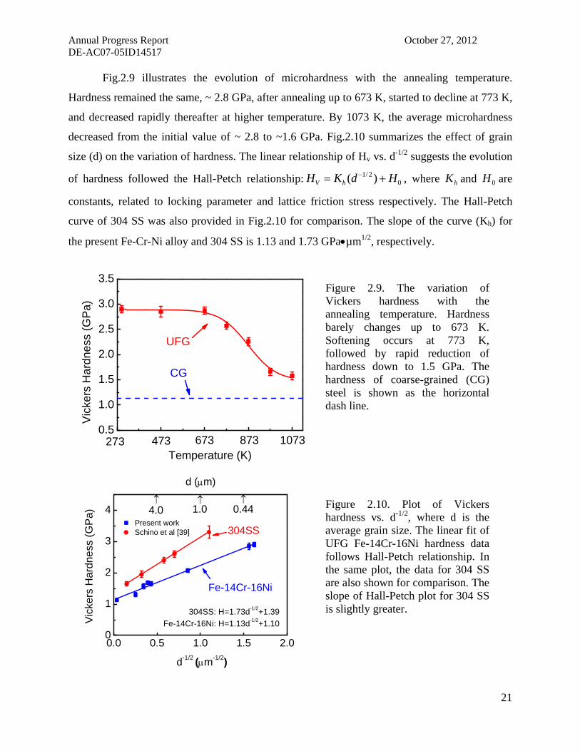
Fig.2.9 illustrates the evolution of microhardness with the annealing temperature.
Hardness remained the same, ~ 2.8 GPa, after annealing up to 673 K, started to decline at 773 K,
and decreased rapidly thereafter at higher temperature. By 1073 K, the average microhardness
decreased from the initial value of ~ 2.8 to ~1.6 GPa. Fig.2.10 summarizes the effect of grain
size (d) on the variation of hardness. The linear relationship of Hv vs. d-1/2 suggests the evolution
of hardness followed the Hall-Petch relationship: 02/1 )( HdKH hV , where hK and 0H are
constants, related to locking parameter and lattice friction stress respectively. The Hall-Petch
curve of 304 SS was also provided in Fig.2.10 for comparison. The slope of the curve (Kh) for
the present Fe-Cr-Ni alloy and 304 SS is 1.13 and 1.73 GPaµm1/2, respectively.
0.5
1.0
1.5
2.0
2.5
3.0
3.5
1073873673473273
CG
Temperature (K)
Vic
kers
Har
dne
ss (
GP
a)
UFG
0.0 0.5 1.0 1.5 2.00
1
2
3
4
Present workSchino et al [39]
4.0 1.0
Vic
kers
Har
dne
ss (
GP
a)
d-1/2 (m-1/2)
d (m)
0.44
304SS
Fe-14Cr-16Ni
304SS: H=1.73d-1/2+1.39
Fe-14Cr-16Ni: H=1.13d-1/2+1.10
Figure 2.9. The variation of Vickers hardness with the annealing temperature. Hardness barely changes up to 673 K. Softening occurs at 773 K, followed by rapid reduction of hardness down to 1.5 GPa. The hardness of coarse-grained (CG) steel is shown as the horizontal dash line.
Figure 2.10. Plot of Vickers hardness vs. d-1/2, where d is the average grain size. The linear fit of UFG Fe-14Cr-16Ni hardness data follows Hall-Petch relationship. In the same plot, the data for 304 SS are also shown for comparison. The slope of Hall-Petch plot for 304 SS is slightly greater.
Annual Progress Report October 27, 2012 DE-AC07-05ID14517
22
Heavily deformed metals with a large fraction of high angle grain boundaries can
continuously recrystallize during annealing. Humphreys et al have shown that a cellular structure
will become resistant to discontinuous growth once ~ 70% of boundaries are high angle grain
boundaries, because on average the cell boundaries will approach the conditions where they have
similar grain boundary energy and mobility. However, the UFG Fe-Cr-Ni alloy, with ~ 90% of
high angle grain boundaries (based on EBSD results that are not shown here), still show the
abnormal grain growth at ~ 873 K. There are two possible mechanisms that lead to the abnormal
grain growth in the current study. First, during ECAP process there is inhomogeneous
accumulation of dislocations within grains and coexistence of high-angle and less mobile low-
angle grain boundaries, thus there may be a large difference in the stored energy both within the
grains and at different type of grain boundaries. The difference in stored energy provides the
driving force for grain boundary migration. It is likely that recrystallization occurs preferentially
in the regions with greater stored energy, leading to rapid growth of grains locally and thus the
bimodal distribution of grain size. Second, the martensite particles might also contribute to the
abnormal grain growth. At the early annealing stage at 873K, the martensite grains, acting as
second phase particles, may generate pinning pressure on the grain boundaries. The competition
between the pinning pressure and driving force for grain growth determines whether the grains
should be stabilized or coarsen. Meanwhile, the inhomogeneous distribution of the martensite
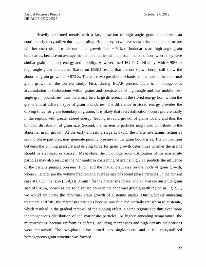
particles may also result in the non-uniform coarsening of grains. Fig.2.11 predicts the influence
of the particle pinning pressure (Fv/dp) and the matrix grain size on the mode of grain growth,
where Fv and dp are the volume fraction and average size of second phase particles. In the current
case at 873K, the ratio (Fv/dp) is 0.3µm-1 for the martensite phase, and an average austenite grain
size of 0.4µm, shown as the solid square point in the abnormal grain growth region in Fig 2.11,
we would anticipate the abnormal grain growth of austenite matrix. During longer annealing
treatment at 873K, the martensite particles became unstable and partially transform to austenite,
which resulted in the gradual removal of the pinning effect in some regions and thus even more
inhomogeneous distribution of the martensite particles. At higher annealing temperature, the
microstructure became uniform as defects, including martensites and high density dislocations
were consumed. The two-phase alloy turned into single-phase, and a full recrystallized
homogeneous grain structure was formed.

Annual Progress Report October 27, 2012 DE-AC07-05ID14517
23
The activation energy for grain boundary and volume diffusion of iron in α-iron is 164
and 280 kJ/mol, respectively. Smith and Gibbs reported activation energy for grain boundary
diffusion (180 kJ/mol) and volume diffusion of iron (284 kJ/mol) in Fe-Cr-Ni-Nb stainless steel.
Our measured average activation energy for normal grain growth, ~207 kJ/mol, is somewhere
between these values, but closer to the activation energy for grain boundary diffusion. In the
ECAPed Fe-Cr-Ni alloy, there are several important factors that dictate the activation energy of
grain growth. First, high density of dislocations in grain interiors and near grain boundaries leads
to an increase in stored energy and driving force for grain growth. Second, a large volume
fraction of high-angle grain boundaries increases atomic mobility and enhances the possibility of
grain boundary migration. Third, phase boundary (between austenite and martensite) also assists
the migration of grain boundaries. Finally, solutes (Cr and Ni) in the alloy increase the bond
strength and thus lower the atomic mobility and increase the activation energy for grain
coarsening. The first three factors can reduce the activation energy of grain growth in
comparison to lattice diffusions, and may play dominant roles in determining the relatively low
activation energy of grain growth in the current study.
0.0 0.1 0.2 0.3 0.4 0.50
2
4
6
8
10
No growth
873 K873 K 873 K
873 K873 K
Ave
rag
e m
axtr
ix g
rain
siz
e (
m)
Fv/d
p (m-1)
Normalgrowth
Abnormal growth
873 K
973 K
1073 K
Figure 2.11. Map for abnormal and normal grain growth as a function of average matrix grain
size (d) and second phase dispersion level (Fv/dp), where Fv and dp are the volume fraction and
average size of second phase particles [40]. In the present study, d = 0.4 µm, Fv/dp=0.3, the
abnormal grain growth is predicted at 873 K. Without second phase particles after annealing at

Annual Progress Report October 27, 2012 DE-AC07-05ID14517
24
973 K and 1073 K, the normal grain growth occurs. The corresponding microstructures of alloys
are shown on the same plot.
The microhardness of UFG alloys decreased when annealed at 773 K. However
microscopy studies did not reveal noticeable grain growth in this specimen. The softening at 773
K may be a consequence of reduction of dislocation density due to static recovery, and relaxation
of internal residual stress resulting from the annihilation and rearrangement of dislocations. The
softening at higher temperatures (≥ 873 K) is mainly attributed to recrystallization and grain
growth. In addition, the temperature for martensite-to-austenite phase transformation is ~ 900 K
for stainless steel, and for the current UFG alloy, no martensite phase was detected after
annealing at 973 K for 1 hour, based on the EBSD result. Thus, the removal of martensite may
also contribute to softening at higher temperatures. The slope of the Hall-Petch plot of the
present Fe-14Cr-16Ni alloy is less than that in 304SS, indicating a lower resistance of grain
boundaries to the transmission of dislocations. This phenomenon can be understood from several
aspects. First, the average shear modulus of the current alloy is smaller than that of 304 SS due to
a lower Cr concentration. The shear modulus of iron (82 GPa) and nickel (76 GPa) is close to
each other. But Cr has a much greater shear modulus, 115 GPa. Second, impurity and
precipitates such as carbides and sulphides in 304 SS, may exist along grain boundaries, and
hence lead to the enhanced grain boundary resistance to the transmission of dislocations.
In the CG and UFG Fe-Cr-Ni alloy, the grain sizes are submicron or greater, and hence
strengthening follows a typical Hall-Petch type of dislocation pile-up model, i.e. Hv increases
linearly with the increase of d-1/2. When grain size reduces to nanoscale, typically 50 nm or less,
dislocation pile-ups become increasingly difficult, and hence the dislocation bowing mechanism
may govern the hardening behaviors. A different model proposed for nanocrystalline materials
can be used here to predict the peak hardness of the Fe-Cr-Ni alloy. The critical shear stress ( )
for bowing of dislocations is expressed by:
]2
1)ln()2
31[(
)1(2
v
b
Lv
vL
Gb
(3)
where G is the shear modulus, b is the magnitude of Burgers vector, v is the Possion’s ratio.
L is the average length of dislocations, assumed to be 2/1cd , where c is 1.25 in nanoscale
regime. To convert the shear stress to hardness, the estimations of 3 and 3vH are used
in the present study. By using G = 78 GPa, b = 0.254 nm, and v = 0.33, the peak hardness is
Annual Progress Report October 27, 2012 DE-AC07-05ID14517
25
calculated to be ~ 6 GPa when the grain size is reduced to ~ 10 nm. This value is similar to what
has been observed in sputtered nanotwinned 330 SS, where the hardness is ~ 6.5 GPa with
average twin density is ~ 5 nm.
As a model alloy, the microstructure and microhardness of the Fe-Cr-Ni alloy are
thermally stable up to 673K. To meet the requirement of future advanced nuclear reactors,
methods, like alloying and addition of oxide particles, will be used to improve thermal stability
and develop radiation resistant structural materials for higher temperature applications.
A3. He ion radiation damage of ultra fine grains in ECAPed Fe-14Cr-16Ni (wt.%) alloys
Lead organization (Texas A&M, Xinghang Zhang)
The Fe-14%Cr-16%Ni ternary alloy, with initial average grain size of 700 µm, was
fabricated by vacuum cast and subsequent hot isostatic pressing. ECAP process was used to
refine the grain size of the Fe-Cr-Ni alloy down to ~ 400 nm. Helium ions at an energy of 100
keV were implanted to coarse grained and ultrafine grained Fe-Cr-Ni alloy at room temperature
to a fluence of 6 × 10¹⁶/cm2. Transmission electron microscopy (TEM) experiment was
performed on a JEOL 2010 transmission electron microscope operated at 200 keV. Cross-
sectional TEM (XTEM) samples were prepared by dimpling and low energy (3.5 keV) Ar ion
milling. The artifacts induced by Ar ion milling were removed by low energy ion polishing
process. Hardness and elastic modulus were measured at room temperature by Fischerscope HM
2000XYp instrument with a Vickers diamond indenter, using instrumented nanoindentation
technique.
SRIM, based on Monte Carlo method, was used to calculate the defect and ion
distribution in Fe-14Cr-16Ni compound irradiated by He ions at 100 keV with a fluence of
6×10¹⁶ ions/cm2. The simulation, as shown in Fig.3.1, predicts that the peak damage induced by
He collisions in the compound is ~ 5.5 dpa at a depth of ~ 250 nm, and the radiation damage
extends to a maximum depth of ~ 480 nm. The peak He concentration, with a value of ~ 4.0
at.%, occurs at a depth of ~ 320 nm.

Annual Progress Report October 27, 2012 DE-AC07-05ID14517
26
0 100 200 300 400 500 600
0
1
2
3
4
5
6
Depth (nm)
DP
A
0
1
2
3
4 He
Con
centration
(at.%)
100 keV
61016/cm2
Figure 3.2. (a) Under focused XTEM micrograph of He ion irradiated CG Fe-Cr-Ni alloy. (b)
The magnified image of region A shows bubbles align along grain boundaries. (c) The magnified
image of region B shows dislocation loops and high density of He bubbles.
Under-focused bright field XTEM micrographs of as-received, coarse grained (CG) Fe-
14Cr-16Ni alloy after He ion irradiation are shown in Fig. 3.2. Fig. 3.2 (a) presents an overview
of the irradiated region, wherein He bubbles can be clearly observed. Magnified micrographs of
Figure 3.1. Depth profile of radiation damage (displacement per atom (DPA)) and Helium concentration obtained from SRIM simulation for Fe-14Cr-16Ni alloy subjected to He ion irradiation at 100keV and a fluence of 6 × 10¹⁶/cm2.
Annual Progress Report October 27, 2012 DE-AC07-05ID14517
27
two regions, A and B in Fig. 3.2 (a), are shown in Fig. 3.2 (b) and Fig. 3.2 (c), respectively.
Bubbles appear at a depth of ~ 100 nm from surface as shown in Fig. 3.2 (b). The maximum
bubble density occurs approximately at 250 nm underneath the surface in ion irradiated Fe-Cr-Ni
alloy, as shown in Fig. 3.2 (c). The black dots in Fig. 3.2(c) are dislocation loops created by
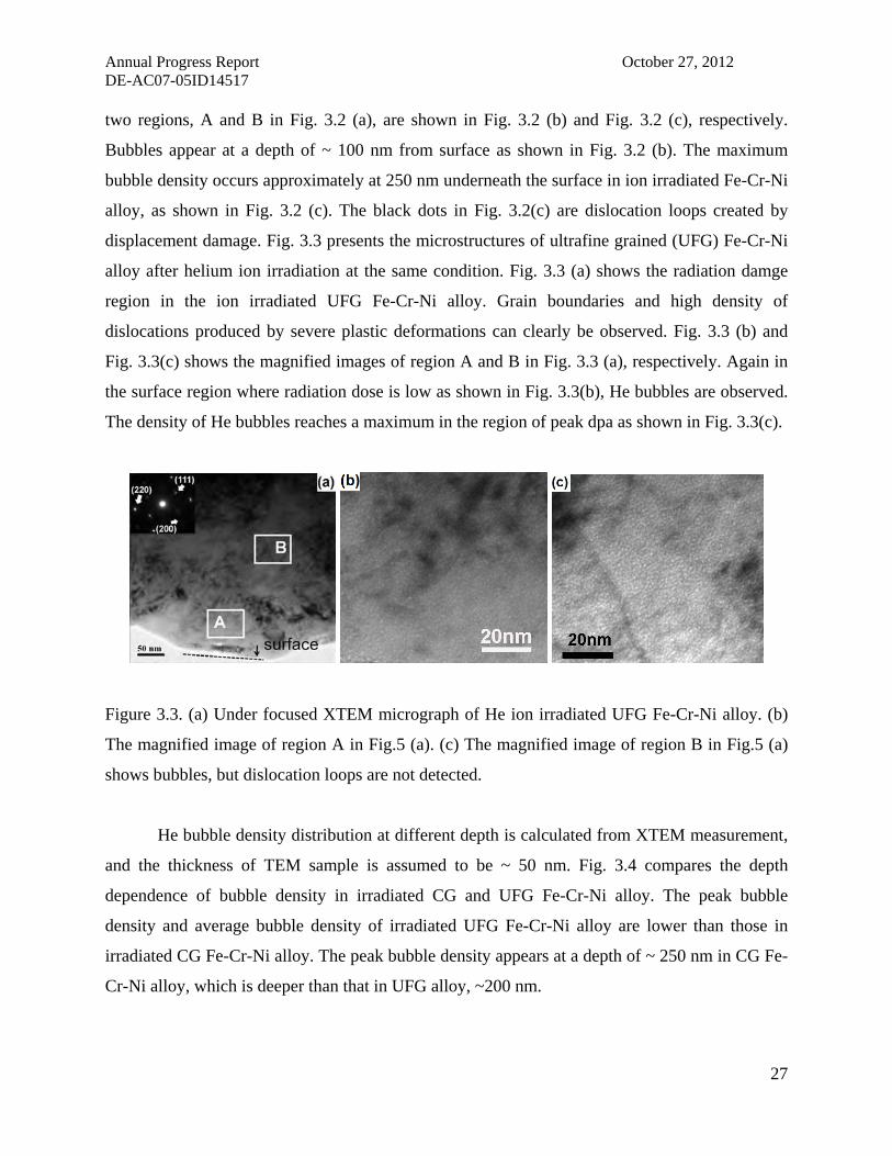
displacement damage. Fig. 3.3 presents the microstructures of ultrafine grained (UFG) Fe-Cr-Ni
alloy after helium ion irradiation at the same condition. Fig. 3.3 (a) shows the radiation damge
region in the ion irradiated UFG Fe-Cr-Ni alloy. Grain boundaries and high density of
dislocations produced by severe plastic deformations can clearly be observed. Fig. 3.3 (b) and
Fig. 3.3(c) shows the magnified images of region A and B in Fig. 3.3 (a), respectively. Again in
the surface region where radiation dose is low as shown in Fig. 3.3(b), He bubbles are observed.
The density of He bubbles reaches a maximum in the region of peak dpa as shown in Fig. 3.3(c).
Figure 3.3. (a) Under focused XTEM micrograph of He ion irradiated UFG Fe-Cr-Ni alloy. (b)
The magnified image of region A in Fig.5 (a). (c) The magnified image of region B in Fig.5 (a)
shows bubbles, but dislocation loops are not detected.
He bubble density distribution at different depth is calculated from XTEM measurement,
and the thickness of TEM sample is assumed to be ~ 50 nm. Fig. 3.4 compares the depth
dependence of bubble density in irradiated CG and UFG Fe-Cr-Ni alloy. The peak bubble
density and average bubble density of irradiated UFG Fe-Cr-Ni alloy are lower than those in
irradiated CG Fe-Cr-Ni alloy. The peak bubble density appears at a depth of ~ 250 nm in CG Fe-
Cr-Ni alloy, which is deeper than that in UFG alloy, ~200 nm.

Annual Progress Report October 27, 2012 DE-AC07-05ID14517
28
0 100 200 300 4000
1
2
3
4
5
6
Bub
ble
dens
ity (
102
4 m-3)
Depth (nm)
CG
UFG
0.4 0.6 0.8 1.0 1.2 1.4 1.6 1.8 2.00
20
40
Num
ber
frac
tion
(%)
Bubble diameter (nm)
UFG
0
20
40
CG
Fig. 3.5 presents the bubble diameter distribution in the irradiated CG and UFG Fe-Cr-Ni
alloy at the peak damage region, obtained by under-focused XTEM micrographs. The average
bubble diameter in irradiated CG and UFG Fe-Cr-Ni alloy is ~1.3 nm and ~1.0 nm, respectively.
Figure 3.4. Depth dependent He bubble density in irradiated CG (open triangles) and UFG (solid squares) Fe-Cr-Ni alloy. He bubble density in the peak damage region is reduced by in UFG alloy. Also the peak bubble density in UFG alloy appears at a shallower depth with respect to film surface.
Figure 3.5. Bubble diameter distribution in the peak damage region of He irradiated CG and UFG Fe-Cr-Ni alloy. The average bubble diameter in CG and UFG Fe-Cr-Ni alloy is 1.3 nm and 1.0 nm, respectively.

Annual Progress Report October 27, 2012 DE-AC07-05ID14517
29
200 400 600 800 1000
0.0
0.5
1.0
Har
dne
ss In
cre
ase
(GP
a)
Depth (nm)
CG Experiment UFG Experiment CG Calculation UFG Calculation
The hardness evolution of CG and UFG Fe-Cr-Ni alloys after ion irradiation is examined
at indentation depth of 200 nm to 1.0 µm and results are shown in Fig. 3.6. The hardness
increase in CG Fe-Cr-Ni alloy is a relatively constant value, ~ 0.9 GPa, when indentation depth
is between 200 and 350 nm. At greater indentation depth, the radiation hardening appears
reduced and finally saturates at a level of ~ 0.35 GPa. The depth dependent radiation hardening
in UFG Fe-Cr-Ni alloy follows a similar trend. But the magnitude of hardening at all depth is
much lower than those in CG specimen. The maximum hardening in UFG specimen is ~ 0.32
GPa, about 65% less than that in the irradiated CG Fe-Cr-Ni alloy at a depth interval of 200-250
nm. Whereas when h > 250 nm, the magnitude of radiation hardening reduces to ~ 0.05 GPa.
The following section presents our interpretations of microstructure evolution and its
correlation to radiation hardening in CG and UFG alloys.
Microstructure evolutions.
Helium bubbles have been observed in both ion irradiated CG and UFG Fe-Cr-Ni alloy.
Compared to irradiated CG materials, the reduction of peak and average He bubble density in
Figure 3.6. Hardness increase (H after ion irradiation-H before ion irradiation) of CG and UFG Fe-Cr-Ni alloy after He ion irradiation as a function of indentation depth. Radiation hardening in CG and UFG Fe-Cr-Ni alloy is indicated by open squares and open triangles, respectively. The calculated radiation hardening due to He bubbles in the peak damage region, shown by solid squares and triangles are compared with experimental values in the same figure.

Annual Progress Report October 27, 2012 DE-AC07-05ID14517
30
irradiated UFG Fe-Cr-Ni alloy indicates that the overall concentration of vacancies must have
been reduced. During radiation, vacancies and interstitials are generated as a result of
displacement cascade. These point defects can be annihilated through direct recombination,
absorbed via pre-existing defects, such as layer interfaces, dislocations, grain boundaries,
cavities, etc., or aggregated into clusters, such as helium bubbles and interstitial loops. ECAP
induced a very high density of high angle grain boundaries as well as dislocations which can act
as effective defect sinks for the recombination of the irradiation induced point defects. And
consequently ECAP specimen should possess lower density of defect clusters, as evidenced by a
lower density of He bubbles and fewer interstitial loops.
The internal pressure in a pressurized helium bubble is expressed by:
rp 2/
where p is the pressure, is the surface energy, mN /2 for stainless steel, and r is the
average radius of the bubbles. The hard sphere equation of state (EOS), Carnahan-Starling EOS,
is applied to calculate the He density in a nano-scale bubble with high pressure at 20°C:
332 )1)(1( yyyyNkT
pV
V
Ndy
6
3
where V is the volume of the bubble, N is the number of the atoms, d is the diameter of the
atom , T is the temperature and k is the Boltzmann’s constant. Based on the above equations,
the average He density in a bubble is 0.21cm3/mol for CG Fe-Cr-Ni alloy, and 0.19 cm3/mol for
UFG Fe-Cr-Ni alloy.
Hardening mechanisms
It is generally accepted that the irradiation induced hardening and embrittlement are
caused by the interaction between dislocations and irradiation-produced obstacles such as defect
clusters, loops, precipitates, void, etc. Two major mechanisms were proposed to explain the
radiation hardening: source hardening, the increase in critical stress required to move a
dislocation on its slip plane due to the pinning effect of the obstacles; and friction hardening,
where the dislocation movement is impeded by the radiation-induced defects lying close to or on
its slip plane. Compared with the friction hardening, the contribution of source hardening is
Annual Progress Report October 27, 2012 DE-AC07-05ID14517
31
relatively small. Two types of radiation induced defects, strong obstacles such as interstitial
loops, and weak obstacles like He bubbles, result in friction hardening. Two dislocation barrier
models, dispersed barrier model for the strong obstacles such as interstitial loops, voids, SFT etc.
and Friedel-Kroupa-Hirsch (FKH) model for weak obstacles like helium bubbles, have been
proposed to describe the radiation induced friction hardening in metals.
In a low temperature range, T 0.4Tm (Tm is the melting temperature), the contribution of
helium bubbles to the radiation hardening is very small at low helium concentration and it
becomes significant only when the He concentration is above a critical value, ~ 1 at.%. SRIM
simulation predicts that the helium concentration in the peak damage region is about 4 at.%. In
this study, the weak obstacle model, FKH model, is used to estimate the radiation induced yield
strength increase, Δσ,
3/2)(8
1NbdM
where M is Taylor factor, 3.06 for FCC metals, µ is shear modulus, b is Burgers vector, d is the
diameter of the bubble, N is bubble density. On the basis of the above model, the calculated
radiation hardening, estimated as three times that of the calculated Δσ, is indicated by solid
squares and triangles for the CG and UFG Fe-Cr-Ni alloy, respectively, in Fig. 3.6. The results
show that the calculated radiation hardening in the peak damage region is comparable to the
experimental value. Besides helium bubbles, dislocation loops may also contribute to the
radiation hardening. It’s difficult to distinguish the helium bubbles induced hardening and
dislocation loops induced hardening. From the XTEM images, the dislocation loop density is
very low and the average loop size is ~ 4 nm, and thus the contribution of dislocation loops is
very small based on the dispersed barrier hardening model.
A4. In situ Kr ion irradiation of coarse grained and nanocrystalline (NC) Ni
Lead organization (Texas A&M, Xinghang Zhang)
NC Ni was synthesized by pulse electrodeposition from sulfamate electrolytes.
Annealing of the as-deposited NC Ni in a vacuum furnace (10-7 torr) at 400°C for 2 hours was
performed to obtain coarse grained (CG) Ni. Plan-view transmission electron microscopy (TEM)
samples were prepared by ion milling and subsequent ion polishing. Convergent beam electron
diffraction (CBED) technique was used to estimate the Ni foil thickness.

Annual Progress Report October 27, 2012 DE-AC07-05ID14517
32
SRIM simulation was used to estimate the displacement damage profile and Kr++ ion
distribution. Displacement energy for Ni, 40 eV, was used to calculate the displacements-per-
atom (dpa). The results show that all the Kr++ ions with energy of 1 MeV will penetrate through
the first 200 nm, whereas displacement damage will be contained primarily in the TEM foil. In
situ Kr++ ion irradiation with energy of 1 MeV was conducted at room temperature in the
Intermediate Voltage Electron Microscope (IVEM) at Argonne National Laboratory, where an
ion accelerator is attached to a HITACHI H-9000NAR microscope. The microscope was
operated at 200 kV and kept on during radiation in order to record the microstructural evolution.
The average dose rate was 0.003 dpa/s.
Fig. 4.1a and b show that the average grain size of CG and NC Ni is 2.5 µm and ~ 55 nm
respectively. Fig. 4.2 presents the TEM images of CG Ni after Kr++ ion irradiation at room
temperature to a dose of 1 and 5 dpa. At 1 dpa (Fig. 2a-b) the primary radiation induced defects
were the high-density dislocation loops, as revealed by black (white) dots in the corresponding
bright (dark) field (BF and DF) TEM micrograph. Up to 5 dpa, dislocation loops joint together to
form high density of dislocation segments and networks as shown in the corresponding BF and
DF TEM micrographs in Fig. 4.2c-d. The loop density was ~ 1.76 ×10²³/m3 at 5 dpa, and density
of dislocation segments increased from ~ 2×10¹²/m2 to ~ 7×10¹³/m2. Defects appeared to
accumulate along the grain boundaries as shown in Fig. 4.2d in form of large bright defect
clusters. The same DF TEM micrograph also revealed high density of dislocation loops in one
grain, and extremely high density of bright stripes in the other grain.
Fig. 4.1 (a) Coarse grained (CG) Ni with an average grain size of 2.5 µm. (b) Nanocrystalline (NC) Ni with an average grain size of 55 nm.

Annual Progress Report October 27, 2012 DE-AC07-05ID14517
33
Fig. 4.2. TEM images of room-temperature, Kr++ ion irradiated CG Ni. (a) After irradiation up to 1 dpa, high density black dots (dislocation loops) were identified. (b) The corresponding dark field (DF) TEM image confirmed the formation of dislocation loops. (c) At 5 dpa, dislocation loops are still evident, and many of the loops joint together to form dislocation segments and
networks. The density of dislocation loops and dislocation segments was ~ 1.76 ×10²³/m3 and 7
×1013/m2. (d) The corresponding DF TEM image revealed the formation of both types of defects.
Fig. 4.3 shows the BF and DF TEM images of irradiated NC Ni to a dose of 1 and 5 dpa.
At 1 dpa and 5 dpa, dislocation loops were observed sporadically in NC Ni. Compared to Fig.
4.2, the defect cluster density was significantly lower in NC Ni, and no significant dislocation
segments were observed.

Annual Progress Report October 27, 2012 DE-AC07-05ID14517
34
Fig. 4.3. TEM images of NC Ni subjected to Kr++ ion irradiation up to 1 and 5 dpa. (a) and (b)
are corresponding BF and DF TEM micrographs of the specimen at 1 dpa. Dislocation loops
were observed sporadically. (c) and (d) are BF and DF TEM micrograph taken at 5 dpa. More
dislocation loops were observed, but no significant dislocation networks were generated. The
density of dislocation loop was ~ 8.40 ×10²²/m3.
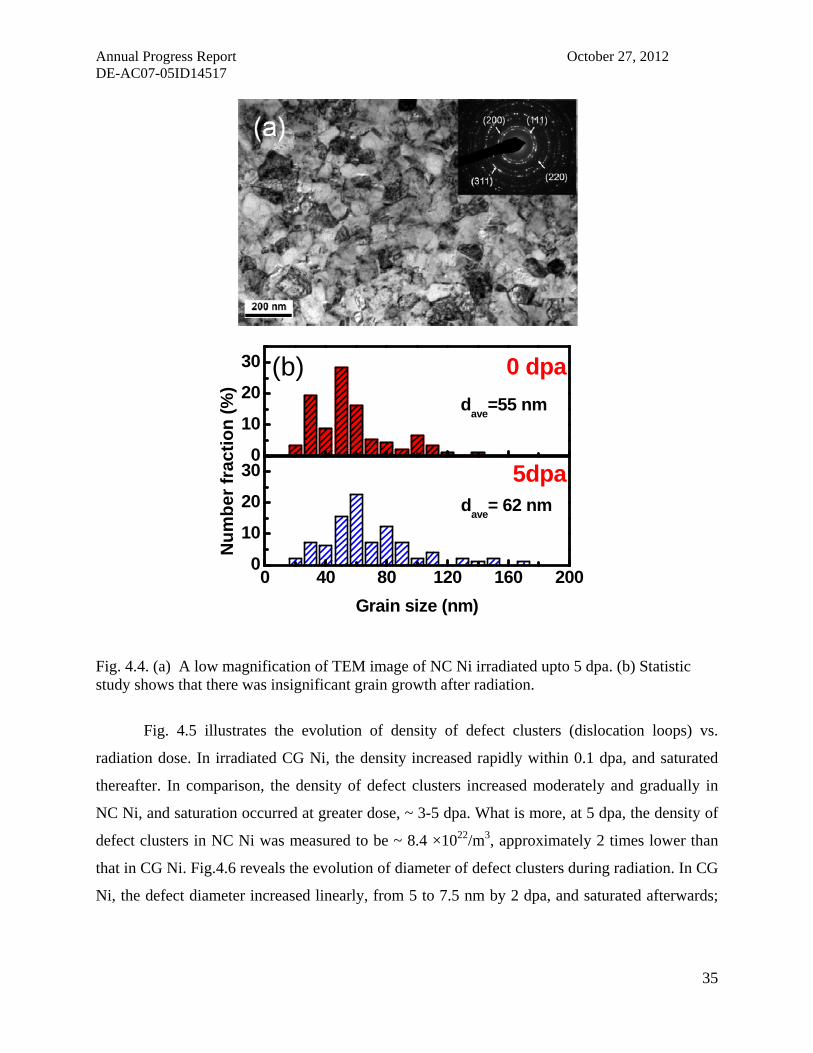
Fig.4.4a shows the low magnification TEM image of NC Ni irradiated to 5 dpa. No
significant grain growth occurred and there was no obvious change of diffraction pattern.
Comparisons of the statistical distribution of grain sizes (Fig. 4.4b) show that, after radiation, the
average grain size slightly increased from 55 to 62 nm.
Annual Progress Report October 27, 2012 DE-AC07-05ID14517
35
0 40 80 120 160 2000
10
20
30
dave
= 62 nm
Nu
mb
er f
ract
ion
(%
)
Grain size (nm)
5dpa0
10
20
30 (b)
0 dpa
dave
=55 nm
Fig. 4.4. (a) A low magnification of TEM image of NC Ni irradiated upto 5 dpa. (b) Statistic study shows that there was insignificant grain growth after radiation.
Fig. 4.5 illustrates the evolution of density of defect clusters (dislocation loops) vs.
radiation dose. In irradiated CG Ni, the density increased rapidly within 0.1 dpa, and saturated
thereafter. In comparison, the density of defect clusters increased moderately and gradually in
NC Ni, and saturation occurred at greater dose, ~ 3-5 dpa. What is more, at 5 dpa, the density of
defect clusters in NC Ni was measured to be ~ 8.4 ×10²²/m3, approximately 2 times lower than
that in CG Ni. Fig.4.6 reveals the evolution of diameter of defect clusters during radiation. In CG
Ni, the defect diameter increased linearly, from 5 to 7.5 nm by 2 dpa, and saturated afterwards;

Annual Progress Report October 27, 2012 DE-AC07-05ID14517
36
whereas in NC Ni, the diameter of defect clusters remained ~ 3.5 nm throughout the radiation
process.
0.01 0.1 1 101022
1023
1024
Def
ect C
lust
er D
ensi
ty (
m-3)
Dose (dpa)
CG Ni
NC Ni
Fig. 4.5. The density of dislocation loops of CG Ni increased rapidly within 0.1 dpa and appeared to reach saturation at ~ 0.5 dpa. Meanwhile the density of loops in NC Ni increased slowly and gradually throughout the radiation up to 5 dpa. Dislocation loop density of CG and NC Ni increases with dose in the beginning stage and then saturates to certain level. At 5 dpa, the average loop density of CG Ni is 2 times greater than that of NC Ni.
0 1 2 3 4 50
2
4
6
8
10
12
De
fect
clu
ste
r di
amet
er (
nm)
Dose (dpa)
CG Ni
NC Ni
Fig. 4.6. Dose dependent evolution of loop diameters. The diameter of loops in CG Ni increased promptly from 5 to ~ 7.5 nm by 2 dpa, and reached a plateau thereafter. In parallel, the loop diameter of NC Ni remained ~ 3.5 nm over the dose of 5 dpa.

Annual Progress Report October 27, 2012 DE-AC07-05ID14517
37
The absorption of dislocation loops by GB was frequently observed during the in situ
Kr++ ion irradiation of NC Ni. Fig.4.7 shows a typical example of microstructural evolution of
NC Ni irradiated over a dose of 1.67 - 1.72 dpa at room temperature, during which the absorption
of individual interstitial loops by GBs was observed. As shown in Fig. 4.7a, an interstitial loop, ~
4.5 nm in diameter, was observed next to GB. With 49 seconds (Fig. 4.7b), the loop diffused
towards the GB and the diameter of the loops shrank to ~ 3.8 nm. After 49.1 s, the loop was
immediately sucked into the GB, and by 49.3 s, a majority of the loop was removed by the GB.
Fig. 4.8 shows an example of frequently observed absorption of dislocation segments by GBs at
a dose spanning over 0.56-0.79 dpa at room temperature in 78 seconds. The arrows identify
several interstitial loops of interest. Initially (Fig. 4.8a) there were three interstitial loops adjacent
to the grain boundary. The closest separation distance between the grains is 8.6 nm. After 13
seconds (Fig. 4.8b), these individual loops combined together into one dislocation segment. By
28 s (Fig. 4.8c) the leading dislocation segment was absorbed by GB. In 78 s (Fig. 4.8d), the
remaining dislocation segment was absorbed by the GB. After radiation, the closest separation
between the two grains reduced to 6.9 nm.
Fig. 4.7. In situ evidence of absorption of individual loops by grain boundaries of NC Ni. The radiation dose increased from 1.67 to 1.72 dpa within 49.3 seconds. (a) The loop, pointed by an arrow, was revealed near grain boundaries. (b) In 49 s, the loop diffused towards the grain boundary accompanied by the continuous reduction of their diameters. (c) By 49.1 s, the loop rapidly migrated towards the grain boundary. (d) By 49.3 s, the loop was fully absorbed and annihilated by the grain boundaries.

Annual Progress Report October 27, 2012 DE-AC07-05ID14517
38
Fig. 4.8. In situ evidence of absorption of dislocation segment by grain boundaries of NC Ni. The radiation dose increased from 0.56 to 0.79 dpa at room temperature within 78 seconds. Interaction between grain boundary and dislocation segment is clearly observed. The arrows represent the dislocation loops. (a) Three discernible dislocation loops were located near the grain boundary, and the closet separation between the two grains is 8.6 nm. (b) With 13 seconds, the loops combine and become one dislocation segments. (c) By 28 second, the dislocation segment was absorbed continuously by the adjacent grain boundary. (d) By 78 seconds, a majority of the dislocation was absorbed except a single dislocation loop in contact with the grain boundary. Meanwhile the closet distance between the two grains is reduced to be 6.9 nm.
From the evolution of the defect density with dose, it is evident that the rate of increase of
defect density in NC Ni is much less than that in CG Ni, and that the saturated density of defect
clusters is also reduced by ~ 50% through grain refinement. These defect clusters were formed
by the aggregation of point defects. Point defects can be removed either through the
recombination of interstitials and vacancies or by the absorption by GBs (as revealed by in situ
experiments), dislocations, and precipitate, etc. In monolithic NC Ni, we assume that GBs are the
primary defect sinks. The concentration of point defects ( C , i for interstitials and v for
vacancies) can be expressed by a chemical rate equation as:

Annual Progress Report October 27, 2012 DE-AC07-05ID14517
39
CDSCCRKt
Cgb
(1)
where t is time, K is the atomic displacement rate; when i , then v ; iD and
vD are the respective diffusion coefficients for interstitials and vacancies; ivR is the
recombination rate of interstitial and vacancy. viviiv rDDR ,)(4 , where vir , is ~ 0.72 nm. gbS
is the GB sink strength. For NC Ni, 2/24 dSgb , where d is grain size, and for CG Ni,
21510 mSgb . iD and vD are calculated based on the migration energy of interstitials and
vacancies, iE and vE , respectively. For Ni at 300K, iE = 0.14 eV, and vE = 1.3 eV. When the
steady state concentration of interstitials and vacancies, siC and s
vC , is reached,
setting 0dt
dC
dt
dC vi , leads to:
2/12 ])2
()([2 iv
gb
iviv
gb
R
DS
D
D
R
K
R
DSC
(2)
Given significant grain size difference in CG Ni (~2.5µm) and NC Ni (~ 55 nm) , we can
calculate the ratio of concentration of interstitials and vacancies in CG and NC Ni at steady state:
/ / 7.87CG NC CG NCi i v vC C C C . This analysis testifies that GBs in NC Ni can effectively reduce
the concentration of point defects.
In situ radiation experiments showed that the density and diameter of dislocation loops in
CG Ni was ~ two times that of NC Ni. For the loops on {111} planes, we estimate the number of
point defects, n, in each dislocation loop by using the relationship:
2/12 )4/3( narL (3)
where Lr is the dislocation loop radius and a is the lattice parameter. Thus, we arrive that
the concentration ratio of point defects in CG and NC Ni is ~ 8, close to the results from
aforementioned calculation.
From in situ radiation experiments, Fig. 4.8, it is clear that the size of the individual
dislocation loops became smaller while the loops moved towards GBs, and eventually being
absorbed rapidly into the GB. In this case, the shrinkage of the dislocation loop and its
absorption by the GB are diffusion-controlled processes, which is most likely to be the diffusion-
controlled climb when the radiation experiments are performed at temperatures below 0.5Tm

Annual Progress Report October 27, 2012 DE-AC07-05ID14517
40
(where Tm is the melting temperature of the specimen). As GBs are sinks for vacancies, the
concentration of the vacancies near GBs will be lower than that in the grain, which leads to a
vacancy concentration gradient near GBs as shown schematically in Fig. 4.9. In the region 2, far
away from the GB, there is a saturation of vacancy concentration induced by radiation. Both
ends of interstitial loops can readily absorb vacancies from the bulk matrix, resulting in the
reduction of loop diameters. In this region, lattice diffusion is the dominant diffusion mechanism.
In region 1, there is a large vacancy concentration gradient adjacent to the GBs. The absorption
of vacancies from one end (towards matrix) of interstitial loops will lead to positive climb
(towards GB). Simultaneously vacancies will be emitted from the other end (facing GB) of
interstitial loop and hence will induce a negative climb. Both processes (absorption and emission
of vacancies) will lead to migration of dislocation loops towards GBs. Thus, the rate of migration
is expedited in the region close to GBs. The climb rate depends on the emission rate (Kem ) and
absorption rate (Kab) of vacancies. When Kem < Kab, the loop diameter will shrink during climb.
If Kem=Kab, a fast conservative climb via pipe diffusion will occur. The rate of absorption of the
dislocation loops by GBs depends on at least the following two factors. First, the separation
distance between loops and GBs. At a large separation distance, loops perform random walk by
lattice diffusion, experiencing insignificant influence of the GBs. Second, the loop diameter.
More vacancies need to be absorbed and/or emitted for the loops of larger diameter, increasing
the activation energy for pipe diffusion. The in situ studies presented here showed that individual
loops are more readily absorbed by GBs than a string of loops, i.e., dislocation segments. Wirth
et al. also reported that the smaller cluster is more mobile than larger ones at low temperature.
In the bulk region (region 2), where the lattice diffusion dominates, from migration
distance observed during in situ experiments, we estimate the diffusivity D to be ~ 2.2 nm2/s by
using the Brownian diffusion model. Based on Arrhenius’s law, the migration energy for
dislocation loops in this region is estimated to be ~ 0.28 eV. This value is very close to the
calculated activation energy for bulk diffusion in Ni, ~ 0.2 eV, in which the dislocation loops
have diameters of ~ 3.5 nm. In the region near the GBs (region 1), the pipe diffusion is the
dominant process for the climb of dislocation loops. The total diffusivity, totalD , can be explained
by Hart dislocation pipe diffusion:
)exp(01 kT
EgDDD p
total (3)
Annual Progress Report October 27, 2012 DE-AC07-05ID14517
41
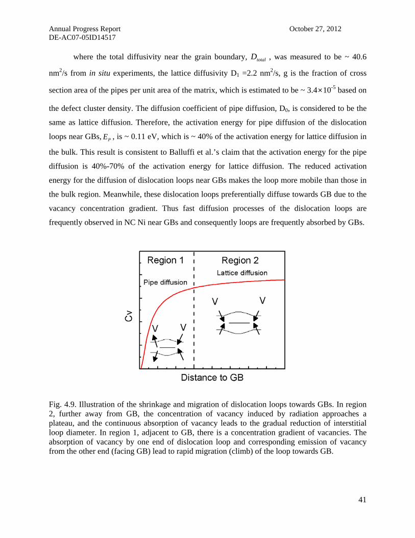
where the total diffusivity near the grain boundary, totalD , was measured to be ~ 40.6
nm2/s from in situ experiments, the lattice diffusivity D1 =2.2 nm2/s, g is the fraction of cross
section area of the pipes per unit area of the matrix, which is estimated to be ~ 3.4×10⁻⁵ based on
the defect cluster density. The diffusion coefficient of pipe diffusion, D0, is considered to be the
same as lattice diffusion. Therefore, the activation energy for pipe diffusion of the dislocation
loops near GBs, PE , is ~ 0.11 eV, which is ~ 40% of the activation energy for lattice diffusion in
the bulk. This result is consistent to Balluffi et al.’s claim that the activation energy for the pipe
diffusion is 40%-70% of the activation energy for lattice diffusion. The reduced activation
energy for the diffusion of dislocation loops near GBs makes the loop more mobile than those in
the bulk region. Meanwhile, these dislocation loops preferentially diffuse towards GB due to the
vacancy concentration gradient. Thus fast diffusion processes of the dislocation loops are
frequently observed in NC Ni near GBs and consequently loops are frequently absorbed by GBs.
Fig. 4.9. Illustration of the shrinkage and migration of dislocation loops towards GBs. In region 2, further away from GB, the concentration of vacancy induced by radiation approaches a plateau, and the continuous absorption of vacancy leads to the gradual reduction of interstitial loop diameter. In region 1, adjacent to GB, there is a concentration gradient of vacancies. The absorption of vacancy by one end of dislocation loop and corresponding emission of vacancy from the other end (facing GB) lead to rapid migration (climb) of the loop towards GB.

Annual Progress Report October 27, 2012 DE-AC07-05ID14517
42
A5. Microstructure Refinement of a 12Cr ODS Steel by Equal Channel Angular
Lead organization (Texas A&M, Xinghang Zhang, K. Ted Hartwig)
The ODS steel powders were prepared by mechanical alloying (MA). The elemental
powders were blended with 70 micron of Fe particles, Cr, Ta, V, and W particles of less than 10
microns in diameters, and 20 nm yttrium oxide (Y2O3) nanoparticles. The MA processes were
carried out using a planetary ball mill operated in a glove box protected by UHP Argon gas. The
ball-to-powder ratio was 15:1. The milling time was typically 12 hrs. After degassing, the ball
milled powders were consolidated by HIPping (hot isostatic pressing) at 1150 °C for 4 h under
100 atm pressure. The nominal chemical composition (in wt.%) of the present alloy is 12 Cr, 1.1
W, 0.2 V, 0.14 Ta, 0.002 B and 0.3 Y2O3 with the remainder being Fe. ECAE processes were
carried out on an MTS-controlled hydraulic press with 2.22×10³ kN force capacity. The ODS
rods with diameter of ~ 12 mm were ECAE processed at 700 and 300 °C respectively.
The ECAE processing conditions are summarized in Table 5.1. Processing routes B and
C involved billet rotations of 90° and 180° respectively around their long axis prior to the
sequent extrusion. A sample extruded two passes at 700 ℃ following route C is designated as
2C700. The hardness was measured by an LM 300AT micro hardness tester using a 0.3 kg force
for a loading time of 13 s. X-ray Diffraction (XRD) measurements were carried out on a Bruker-
AXS D8 diffractometer.
Table 5.1 ECAE processing condition with sample identifiers.
Identifiers ECAE route ECAE temperature (°C)
As-Hipped - -
1A300 1 300
2C700 2C 700
2B700 2B 700
Transmission electron microscopy (TEM) was performed using a JEOL 2010
transmission electron microscope operated at 200 kV. Selected area diffraction (SAD) patterns
were obtained by using an aperture with a diameter of 1.3 µm. High Resolution TEM (HRTEM)
and scanning transmission electron microscopy (STEM) were performed on an FEI Tecnai F20

Annual Progress Report October 27, 2012 DE-AC07-05ID14517
43
microscope equipped with a high angle annular dark field (HAADF) detector and an Oxford
instruments EDX detector. TEM specimens were electro polished using 10% (volume fraction)
perchloric acid methanol solution at -20 °C. Scanning electron microscopy (SEM) was
performed on an FEI Quanta 600 microscope operated at an acceleration voltage of 20 kV with a
working distance of 10 mm. The SEM samples were electrochemically etched with a KOH
solution, which selectively etched the Cr rich phases.
The as-HIPped ODS sample had a bimodal structure as shown by the representative TEM
micrograph in Fig.5.1a. The average size of coarse grains was about 2.5 µm and the maximum
grain size was ~ 8 µm. The surrounding ultrafine grains were 400 ~ 500 nm in diameter. After
2C processing (2C700), the maximum dimension of coarse grains was effectively refined to
below 2 µm and all grains became more equiaxed as shown in Fig.5.1b. When applying route B
at the same temperature (2B700), although the same amount of strain was introduced into the
specimen, the volume fraction of non-equilibrium grain boundaries and fine grains is greater as
shown in Fig.5.1c. After processing via 1A300, a smaller grain size was achieved (Fig.5.1d)
compared to that in 2B700. In the ultrafine grain zone, shown in Fig.5.2, grain refinement was
not as pronounced. The density of dislocations in grains significantly increased (Fig. 5.2c-d).
Also, a greater fraction of high-angle grain boundaries was observed in the 1A300 material as
shown by discontinuous rings in the inserted SAD pattern. The d-spacing measurement showed
that this steel had predominantly BCC structure, which was confirmed by the XRD profiles (not
shown here).
Annual Progress Report October 27, 2012 DE-AC07-05ID14517
44
Fig. 5.1.(a) Bright field TEM micrograph of as-HIPped ODS steel having a bimodal structure with larger grains of several microns and puddles of small grains of ~ 460 nm in diameter; (b-d) are TEM micrographs of ODS steel following 2C700, 2B700 and 1A300 ECAE processes.
Fig. 5.2. Comparisons of ultra-fine grains in as-HIPped and ECAE processed ODS steels. (a) Ultra-fine grains in as-HIPped ODS steel exhibit interiors that are relatively free of dislocations. After ECAE processing at (b) 2C700, (c) 2B700 and (d) 1A300, the density of dislocations in
Annual Progress Report October 27, 2012 DE-AC07-05ID14517
45
grains increases significantly. The inserted selected area diffraction (SAD) patterns show that the ODS steels subjected to ECAE processing have predominant BCC structure.
Fig. 5.3. HRTEM images of nanoscale oxide particles in the as-HIPped alloy: (a) medium-size spherical Y2O3 particle, about 8 nm in diameter with corresponding (b) FFT pattern shows the orientation relationship between the Y2O3 particle and matrix. The zone axis of the oxide particle
is [110]. (c) A 4 nm oxide nanoparticle indexed as Y2O3 examined along its [1 2
1] zone axis; and (d) a larger faceted oxide particle examined along the same zone axis as the oxide particle in (a) revealed clear phase boundaries between oxide and matrix.

Annual Progress Report October 27, 2012 DE-AC07-05ID14517
46
HRTEM examination was performed to determine the crystalline structure of the oxide
particles. As shown in Fig.5.3a, many oxide nanoparticles appear spherical with diameters of ~ 8
nm. Fast Fourier transform (FFT) of the micrograph, in Fig.5.3b, shows that the oxide particle
had a BCC Y2O3 structure with a lattice parameter of 1.06 nm. The diffraction dots near the
central beam are from the secondary diffraction of the matrix spots. The orientation relationship
between the crystalline oxide particles and the matrix (denoted as phase) derived from FFT
pattern was determined to be (020)α // (00 4
)Y2O3 and [001]α //[110]Y2O3. Smaller and larger oxide
particles were also characterized. Many larger oxide particles (Fig.5.3d) had a faceted shape
rather than the spherical shape of smaller particles. The corresponding FFT patterns show crystal
structure similar to the medium sized particles.
Fig 5.4. TEM micrographs show that (a) oxide particles were randomly distributed in the as –HIPped ODS steel. (b) Oxide particles decorate the grain boundaries of ultra-fine grains in as-HIPped specimen. (c) After ECAE (2B700), oxide particles were more uniformly distributed throughout grains. (d) Numerous oxide particles in ECAE processed samples (1A300) were deformed via shear.

Annual Progress Report October 27, 2012 DE-AC07-05ID14517
47
Fig.5.4a shows that oxides particles are well distributed inside certain grains of the as-
HIPped specimen. Other types of precipitates (Cr rich oxide particles) as indicated by circles
were also observed. A non-uniform distribution of the oxides within other larger grains was also
observed. For instance numerous oxide particles were arranged preferentially along grain
boundaries in the primary ultrafine grain region (Fig.5.4b). After ECAE at 700 °C, oxide
particles were more uniformly distributed inside grains as shown in Fig.5.4c. When applying
single pass ECAE at a lower temperature, 300 °C, triangular or elliptic shaped oxide particles
were observed as marked by arrows in Fig.5.4d. A close examination of oxide nanoparticles
shows that their structure remained BCC Y2O3 with a lattice parameter of 1.06 nm as shown in
Fig.5.5a. Some of the oxide nanoparticles tended to evolve into smaller particles (Fig.5.5b).
Fig 5.5. (a) HRTEM images of nanoscale oxide particles in specimen 1A300. The FTT patterns (upper-right from the 20 nm and lower-left from the 5 nm diameter Y2O3 oxides) show that the
oxide particles remained BCC in crystal structure (zone axis along [1
21
]). (b) Numerous oxide nanoparticles were deformed by shear stress.
Other types of precipitates were investigated further in as-HIPped specimens. Fig.5.6a
shows a “palm like” precipitate tilted to a perfect [110] zone axis. This precipitate has an FCC
structure with a lattice parameter of 1.07 nm as confirmed by the inserted SAD pattern. A STEM
image of the same location is shown in Fig.5.6b. Chemical analysis (Fig.5.6c) reveals that the
precipitate has the stoichiometry of (Cr, Fe)23C6. Other Cr rich oxide particles were also
detected. As shown in Fig.5.7a (TEM) and 7b (STEM mode), a larger particle with ellipsoidal

Annual Progress Report October 27, 2012 DE-AC07-05ID14517
48
shape was identified with the shorter dimension of ~ 500 nm. According to the EDX line scan
result, Fig.5.7c, the particle was Cr rich oxide. The enrichment of Cr inside the particle led to the
depletion of Cr in surrounding matrix. The same type of particles was also investigate by SEM
(after selectively etching by KOH solution) as shown in Fig.5.7d in order to obtain statistical
distribution of particle sizes. No pronounced geometry change was observed for the Cr oxide
particles and Cr carbides after ECAE according to the SEM results (not shown here).
Fig 5.6. (a) Bright field TEM image and the corresponding SAD pattern of (Cr, Fe)23C6 particles
in as-HIPped ODS steel; (b) STEM image of the same region and (c) the corresponding
compositional profile along line scan (black line in (b)) showing chemical composition changes
along this line.
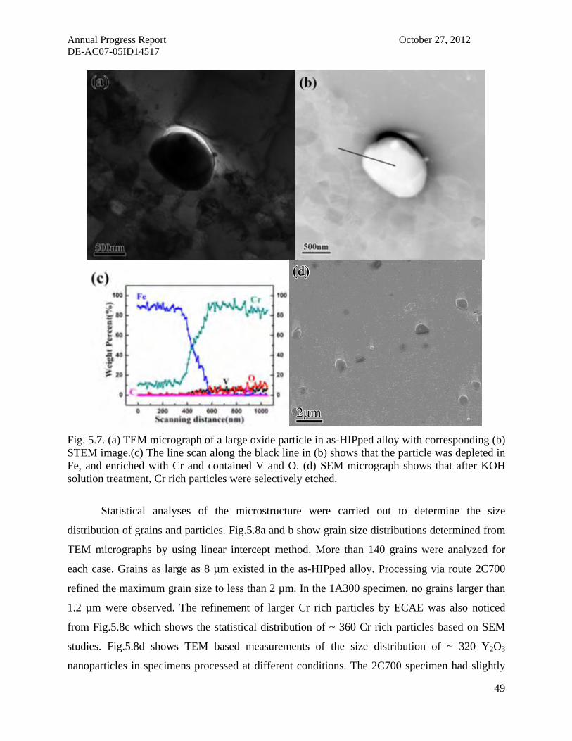
Annual Progress Report October 27, 2012 DE-AC07-05ID14517
49
Fig. 5.7. (a) TEM micrograph of a large oxide particle in as-HIPped alloy with corresponding (b) STEM image.(c) The line scan along the black line in (b) shows that the particle was depleted in Fe, and enriched with Cr and contained V and O. (d) SEM micrograph shows that after KOH solution treatment, Cr rich particles were selectively etched.
Statistical analyses of the microstructure were carried out to determine the size
distribution of grains and particles. Fig.5.8a and b show grain size distributions determined from
TEM micrographs by using linear intercept method. More than 140 grains were analyzed for
each case. Grains as large as 8 µm existed in the as-HIPped alloy. Processing via route 2C700
refined the maximum grain size to less than 2 µm. In the 1A300 specimen, no grains larger than
1.2 µm were observed. The refinement of larger Cr rich particles by ECAE was also noticed
from Fig.5.8c which shows the statistical distribution of ~ 360 Cr rich particles based on SEM
studies. Fig.5.8d shows TEM based measurements of the size distribution of ~ 320 Y2O3
nanoparticles in specimens processed at different conditions. The 2C700 specimen had slightly

Annual Progress Report October 27, 2012 DE-AC07-05ID14517
50
greater Y2O3 particles. Details of microstructural features are given in Table 5.2. The average
grain size of the matrix was reduced by a factor of two after processing via 1A300. In addition,
both the size and volume fraction of Cr rich oxide particles were reduced by ECAE processing.
The density of oxide particles was little affected, on the order of 1022/m3.
Fig.5.9 shows a Hall-Petch plot, i.e. the dependence of hardness on d-1/2, where d is the
average grain size. The hardness increased from 2.4 (as-HIPped) to 3.2 GPa (~35%) after ECAE,
and followed a linear relationship with d-1/2.
Fig. 5.8. Grain and particle distributions in as-HIPped and ECAE processed ODS alloys. (a)
Grain size distribution in as-HIPped sample shows that grains as large as 8 µm existed after
consolidation. (b) Grain size distributions showed grain refinement after ECAE processing. (c)
Cr rich particles were also refined after ECAE. (d) Insignificant variation of distribution of Y2O3
oxide particles after ECAE except that the average particle size appeared to increase slightly in
2C700 specimen.

Annual Progress Report October 27, 2012 DE-AC07-05ID14517
51
Fig. 5.9. Hall-Petch plot of ODS steels with average grain size varying from 300 to 800 nm.
Grain refinement through ECAE led to strengthening of ODS steels.
Table 5.2 Evolution of microstructural features after ECAE
Alloy
ID
Grain Cr rich phase (M23C6 and Cr
oxides)
Y2O3 nanoparticles
Average
size(µm)
Maximum
size(µm)
Average
size (µm)
Volume
fraction (%)
Density
(m-3)
Average
size(nm)
Density(m-
3)
As-
HIPed
0.77±1.09 ≥8 0.40±0.22 2.31±1.31 2.8×10¹⁶ 4.7±2.3 3×10²²
2C700 0.60±0.29 2 0.35±0.23 1.53±0.68 2.5×10¹⁶ 6.5±2.9
2B700 0.50±0.17 1.2 0.33±0.18 1.47±0.51 3.4×10¹⁶ 4.4±2.0
1A300 0.33±0.19 1.2 0.30±0.17 1.25±0.31 3.8×10¹⁶ 4.6±2.4
Microstructure of the as HIPped materials
Bimodal grain structure is commonly achieved by two methods: thermal mechanical
treatment followed by annealing and blending/consolidation of mixed powders with desirable
grain sizes and volume fractions. Zhao et al successfully fabricated bimodal ODS steels by using
blended powder of different sizes. In the present study, large grains were observed probably

Annual Progress Report October 27, 2012 DE-AC07-05ID14517
52
because of abnormal grain growth during HIPping at 1150 °C. No bimodal structure was
observed in EUROFER ODS steel by Lindau et al. This is likely because their alloy was
prepared from gas atomized master alloy, a process that may give less phase segregation. The
consolidation temperature is greater than recrystallization temperature and thus lead to the
bimodal structure.
The average diameter of Y2O3 particles in this study (~ 4.5 nm) is slightly greater than
what had been observed in previous work (≤ 3 nm). This may be related to the absence of Ti in
the current ODS steels. Titanium is apparently beneficial to the formation of smaller oxide
nanoparticles. The orientation relationship between the matrix and Y2O3 particles in the present
study is (020)α // (00 4
)Y2O3 and [001]α // [110]Y2O3. This is similar to previous studies on an FeAl
based ODS alloy although the matrix (FeAl) in that system had a CsCl structure, which is
different from the present BCC structure. Klimiankou et al showed a somewhat different
orientation relationship in EUROFER97 ODS, that is [111]FeCr//[110]Y2O3 and
(11
0)FeCr//(11
1
)Y2O3. These orientation relationships were developed during the HIPping process
as a means to minimize the interface energy between the oxide particles and matrix.
The formation of M23C6 is inevitable because of the contamination of carbon from the
balls and vials used in the MA process. The M23C6 phase was also observed by Klimiankou et al
[48] after heat treatment of a similar alloy. (Fe, Cr)23C6 can lower the ductile-to-brittle-transition-
temperature (DBTT) of the alloys. Cr rich oxide particles frequently observed in the ODS steel
formed because of excessive oxygen in the matrix.
Multi scale microstructural refinement achieved by ECAE
The effect of ECAE on microstructural refinement of the present ODS steels is
summarized as follows. First, the maximum grain size was successfully reduced from several
microns to ~ 1 µm, and a smaller average grain size with a uniform distribution was achieved.
The low temperature extrusion (1A300) was more effective in grain refinement than the high
temperature (2C700 and 2B700) process, even though less strain was applied. ECAE at 700 °C
might have triggered dynamic recrystallization that led to concurrent grain growth during
extrusion. There are two peaks in the grain size distribution chart of the 2C700 samples
(Fig.5.8b). The first peak, ~ 375 nm in average grain size, may arise from the original ultrafine
Annual Progress Report October 27, 2012 DE-AC07-05ID14517
53
grains in the as-HIPped material. The second peak, ~ 600 nm in average grain size, may be
formed by refinement of the larger grains in the as HIPped samples.
Second, the average dimension of Cr rich precipitates (M23C and Cr oxides) was refined
and their volume fraction was significantly reduced by ECAE. The refinement of precipitates
strongly suggests that ECAE is an effective route to redistribute solute, remove precipitates to
some extent, and achieve a more homogeneous microstructure. No fractured particles were
observed in this study. In fact fractured particles induced by ECAE were rarely observed except
for particular shaped particles which had a large stress concentration factor.
Third, ECAE appears to change the distribution and geometry of small Y2O3
nanoparticles. The oxide nanoparticles were not uniformly distributed in the as-HIPped material.
Numerous oxide nanoparticles were found surrounding ultra-fine grains. This is because the
oxide nanoparticles were mechanically mixed with metal powders during milling, and hence
were not fully incorporated uniformly throughout the metal grains even after long duration
mechanical alloying. After ECAE, however, most of the oxide particles were found to be
distributed uniformly throughout the matrix. Furthermore, the shape of numerous oxide particles
in the 1A300 samples was found to be ellipsoidal, implying that large shear stress induced by
ECAE may lead to morphology changes of tiny oxide nanoparticles. Although the average
particle size appeared intact in 1A300 specimens, in numerous cases, oxide nanoparticles
appeared to be “decomposed” into smaller particles (Fig. 5.5b).
4.3 Hardening mechanism
The hardness of ODS steel may be affected by three factors: dispersion strengthening
from Y2O3 particles, from the Cr rich phase, and dislocation pile-ups due to grain refinement
(Hall-Petch relationship).
First, we will estimate dispersion strengthening based on the Orowan bowling
mechanism. For simplicity we assume the system is a simplified Fe-Y2O3 alloy in which Y2O3
nanoparticles are uniformly distributed and the solid solution has negligible effect on hardening.
Dispersion hardening is then calculated by:
0
[ln( ) ]2
GAb DB
r
, (1)
where is the shear stress for bowing of dislocations; b is the magnitude of Burgers vector of a
full dislocation, and which in BCC Fe it can be written as 1/2<111>a (where a is the lattice
Annual Progress Report October 27, 2012 DE-AC07-05ID14517
54
parameter); A=1 and B=0.7 for an edge dislocation; A=1/(1- ν) and B=0.6 for a screw
dislocation. In BCC Fe, b = 0.274 nm, G = 59.7 GPa, and ν = 0.159. G and ν are the shear
modulus and Poisson’s ratio for the {110} <111> slip system, and are calculated to be 3/[4(S11-
S12)+ S44] and (2S44-4S11-8S12)/(6S11+6S12+3S44), respectively, where S11, S22 and S44 are the
compliance factors for iron. r0 is the inner cut-off radius of the dislocation core and is typically in
the range of 1~3 b. λ is the inter particle distance on a slip plane, which is given by,
1.25 2s sl r , (2)
where ls is the center to center distance of particles, and rs is the average radius of oxide particles.
The factor of 1.25 is a conservation coefficient arising from the assumption that the Y2O3 particle
is a strong barrier, and the dislocation segment would be unstable when interacting with pairs of
obstacles with a separation distance above 1.25 ls.
The parameter D is given by equation:
2
2s s
s s
r lD
r l
, (3)
where ls and rs are estimated by using the following equations,
32
3s
rl
f r
(4), and
2
4s
rr
r
, (5)
where r , 2r , 3r are the average value of r, r2, r3, where r is the diameter of a particle. f is the
volume fraction of particles. For Y2O3, the volume fraction of particles was estimated from the
weight fraction given a material density of 5.01 g/cm3.
The hardness was estimated by,
3 yH , (6)
where H is the Vickers hardness and σy is the yield strength of the material. A similar estimate of
strengthening was carried out for the Cr rich precipitates. Results are given in Tables 5.3 and 5.4.
Table 5.3 Parameters for Orowan strengthening by Y2O3 nanoparticles.
Processing (10- (10- (10- ls(10- rs(10- f λ(10-9 τs H(MPa)

Annual Progress Report October 27, 2012 DE-AC07-05ID14517
55
condition 9 m) 18 m2) 27 m3) 9 m) 9 m) (vol.%) m) (MPa) As Hiped 4.7 27.7 221 145 4.6 0.47 172 43~
67 127~206
2C700 6.5 50.3 494 183 6.1 0.47 218 37~57
108~167
2B700 4.4 23.1 163 128 4.1 0.47 152 47~74
137~225
1A300 4.6 27.6 217 148 4.7 0.47 172 44~68
127~206
Table 5.4 Parameters for Orowan strengthening by Cr rich phases.
Processing condition
(10-6
m) (10-
12m2) (10-
18 m3) ls(10-
6 m)
rs(10-
6 m) f (vol.%)
λ(10-6
m) τs
(MPa) H(MPa)
As Hiped 0.40 0.21 0.13 5.43 0.41 2.31 5.96 3.0~4.0
8.8~11.8
2C700 0.35 0.17 0.12 6.85 0.38 1.53 7.80 2.3~3.1
6.9~8.8
2B700 0.33 0.14 0.08 5.88 0.33 1.47 6.68 2.6~3.5
7.8~10.8
1A300 0.30 0.12 0.06 5.79 0.31 1.25 6.61 2.6~3.5
7.8~10.8
The magnitude of dispersion strengthening arising from both oxide particles and Cr rich
precipitates is small, varying from 10 to 200 MPa. This is insufficient to explain the magnitude
of strengthening observed in ECAE processed ODS steels.
A linear relationship between hardness and the square root of the grain size was observed
(Fig.5.9), implying that dislocation pile-up against high angle grain boundaries is the
predominant hardening mechanism, which is described by the Hall-Petch relationship. The
smallest average grain size in ECAE processed material is ~ 330 nm, a range for which the
abundant pile-up of dislocations remains available. The Hall-Petch type of hardening mechanism
is frequently observed for metallic materials subjected to sever plastic deformation.

Annual Progress Report October 27, 2012 DE-AC07-05ID14517
56
A6. Heterogeneous Nucleation and Growth of Oxide Particles in a 12Cr ODS Steel
Lead organization (Texas A&M, Xinghang Zhang, K. Ted Hartwig)
For the ODS alloys without Ti, single phase of Y2O3 particles was reported by the study
of TEM (transmission electron microscope) as the main formula of the particles. However,
detailed studies by FIM (field ion imaging) or EELS (electron energy loss spectrum ) reveal that
the particles have core-shell structures with Y, O and Mn in the cores and a V, Cr, Ta rich shell
dependent on the chemical composition in different ODS steels, which is complicated as
expected. The minor additional elements like V or Mn may play an important role as Ti does.
Although open to question, the formation of core-shell structures of the oxide particles are
explained mainly through two alternative mechanisms. The first mechanism considers shell as a
means of segregation of elements to the particle/matrix interface during the sequent cooling after
the particles were formed. The second mechanism explains the presence of the shell as necessary
to decrease the interfacial energy.
In this study, another configuration of Yttrium oxide and Chromium oxide was observed
first time instead of core-shell structure. These embedded or back to back structures of oxides
particles can serve as the supplemental understanding of the nature of the core-shell structure and
the nucleation and growth of the complex oxide particles. Alternative mechanisms are proposed
to explain the phenomenon.
The material investigated in present study was a reduced activation ferritic ODS steel,
prepared by typical processing including mechanical alloying (MA) the blended powders,
degassing and subsequent HIPping (hot isostatic pressing) process. The original sizes of powders
were 70µm of Fe, ≤10 µm of Cr, Ta, V, W and 20nm of yttrium oxide (Y2O3). MA processes
were carried out using a planetary ball mill operated in a glove box protected by ultra high purity
Argon gas. The ball-to-powder ratio was 15:1. The milling time was typically 12 hrs. The
HIPped condition was selected to be 1150℃ for 4hrs under 100 atm pressure. The nominal
chemical composition (in wt.%) of the present alloy was 12 Cr,1.1 W,0.2 V,0.14 Ta, 0.3 Y2O3
with the remainder being Fe. Post process heat treatments were carried out in quartz tube with
the protection of high purity Argon gas. 1300 ℃ annealing was carried out in sealed quartz tube
with the protection of high purity Argon gas in furnace. All the samples were furnace cooled.
The TEM specimens were prepared by mechanical grinding of 3 mm disks down to 50 µm. The
disks were then etched in a twinjet polisher with 10vol.% perchloric acid + 90vol.%methyl

Annual Progress Report October 27, 2012 DE-AC07-05ID14517
57
alcohol solution with voltage 15 ~ 30 V at -40°C. The ion milling was used as a cutting-open
method of the particles with applied energy of 3.5 kv for 5 min after electro polishing. The
microstructure and chemical analysis were performed on FEI Tecnai F20 field emission gun
TEM equipped with HAADF (high angle annular dark field) detector for STEM and Oxford
instruments EDX detector. Scanning electron microscopy (SEM) was performed on an FEI
Quanta 600 microscope operated at an acceleration voltage of 20 kV with a working distance of
10 mm. The SEM samples were electrochemically etched with a 10g/100ml KOH solution with a
voltage of 10V, which selectively etched the Cr rich phases.
Fig. 6.1. (a) Bright field TEM micrograph of as-HIPped 12-Cr ODS steel having a bimodal structure, i. e. larger grains, ~several microns in diameters, and puddles of ultrafine grains, ~250nm, spotted with black chromium oxide particles (b) Corresponding STEM image of the same region show the chemistry and thickness contrast from chromium oxide particles with various sizes.
Fig.6.1 (a) showed the representative TEM micrograph of the as-HIPped ODS steel after
electro polishing. The as-HIPped ODS steel showed a bimodal grain size structure with average
sizes about 1.7 µm of coarse grains and 250 nm of ultrafine grains (based on a statistic of 230
grains totally, grain size ≥900 nm was taken as coarse grains, others as ultrafine grains). The
black dots located at grain boundaries were Cr rich oxides. The grain boundaries as a high
diffusion path can accelerate the growth of the particles. The enrichment of Cr in the particle led

Annual Progress Report October 27, 2012 DE-AC07-05ID14517
58
to the depletion of Cr content near it, which deteriorated the corrosion resistance of the matrix
around and thus made the corrosion property discontinuous. Holes were generated at the
interfaces between the particles and matrix. Fig.6.1 (b) was the STEM image giving the chemical
contrast of the same region. The Cr rich oxides should show darker contrast for the relatively low
atomic number. But the higher thickness caused by the corrosive properties enhanced the elastic
scattering of the electrons and also shorten the distance to the detector. These factors made the
contrast of the particles brighter.
Fig. 6.2. (a) TEM micrograph of complex oxide particles in as-HIPped ODS steel with (b-g) corresponding STEM elemental mappings of Y, V , Fe, Cr, O and C.
These kind of large oxide particles existing were analysis through STEM mapping and
line scanning in either as-HIPped or annealing ODS alloy after ion milling. These large particles
located at both intragranularly and intergranularly. Fig.6.2 showed the bright field image of a
cutting-open complex oxide particle and corresponding elemental mappings. This particle
located at the grain boundaries. The center was found to be a YCrOx type particle with all of its
edges were surrounded by Cr rich oxide or Y rich oxide particles. The two Cr rich particles were
detected with similar chemical composition but different orientations. V was also detected within
the Cr rich particles. In the Y rich oxide particles, small amount of Cr was also detected. None of
elements such as C, Fe, Ta and W was detected within the particles.

Annual Progress Report October 27, 2012 DE-AC07-05ID14517
59
A large oxide particle after annealing at 900℃/10h was also shown in Fig.6.3a. This
particle located at the grain boundaries of the ultrafine grain zone. Three smaller particles were
Fig. 6.3. (a) TEM micrograph of yttrium oxide nanoparticles inside of chromium oxide particle after annealing (900℃/10h) (b) Corresponding STEM image of the same particle; (c-e) The line scan along the white arrows c, d, e in (b) shows that the chemical composition change. Particles of yttrium oxide were indentified in (c) and (e), whereas complex oxidized chromium carbide was indentified in (d).

Annual Progress Report October 27, 2012 DE-AC07-05ID14517
60
observed within the larger particle. Fig.6.3c-e confirmed the chemical composition of the three
particles in position illustrated in Fig.6.3b. Two of them were yttrium oxides and the other was
carbide. One of yttrium oxide was totally surrounded by the chromium oxide particle. The other
remained half surrounded. None of small Y2O3 particles below 20nm was observed in the large
particles. Intragrannular large oxide particles were also observed.

Annual Progress Report October 27, 2012 DE-AC07-05ID14517
61
Fig. 6.4. Comparison of dual-phase intragranular oxide particles in as-HIPped and annealed alloy (a) TEM micrograph of a dual-phase oxide particle, ~200nm in diameter, in the as-HIPped 12-Cr ODS steel;(b) STEM image of the same particle;(c) The EDX line scan along the white arrow in (b)shows that the two particles are mainly chromium oxide and yttrium oxide, respectively (d) TEM micrograph of a dual phase oxide particle after annealing (1300℃/10h) (e) The corresponding STEM image of the particle (f)The line scan across the particle indicated that the two particles are mainly chromium oxide and yttrium oxide.
Fig.6.4 showed the cutting-open particles in both as-Hipped (Fig.6.4a-c) and after
1300℃/10h annealing (Fig.6.4d-f) state within the matrix. The two oxides exhibited coherence
boundaries as shown in Fig.6.4a. The black particle in Fig.6.4b was chromium oxide and the
white particle adjacent to it was yttrium rich oxide particle, both of which were confirmed by the
EDX shown in Fig.6.4c. Small Y2O3 particles with size less than 20 nm were also observed
within chromium oxide particle. The two oxides formed a broken line interface. Stress formed
around the corner of interface within chromium oxide indicated by the change of contrast. At the
corner, the lattice parameters of chromium oxide need to match those of yttrium rich oxide
particle along two different crystalline directions simultaneously. This stress can play an
important role in the coherence and the change of the shape of the yttrium rich oxide during
annealing. Another intragranular particle was a combination of chromium oxide and yttrium
oxide with similar size in Fig.6.4d. The chemical contrast was given in Fig.6.4e by the STEM
image with confirmed line scanning shown in Fig. 6.4f. This kind of particles with similar size of
both oxides was seldom observed in as-HIPped alloy.
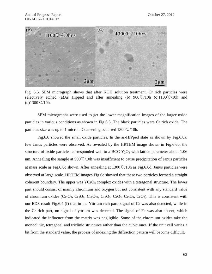
Annual Progress Report October 27, 2012 DE-AC07-05ID14517
62
Fig. 6.5. SEM micrograph shows that after KOH solution treatment, Cr rich particles were selectively etched (a)As Hipped and after annealing (b) 900℃/10h (c)1100℃/10h and (d)1300℃/10h.
SEM micrographs were used to get the lower magnification images of the larger oxide
particles in various conditions as shown in Fig.6.5. The black particles were Cr rich oxide. The
particles size was up to 1 micron. Coarsening occurred 1300℃/10h.
Fig.6.6 showed the small oxide particles. In the as-HIPped state as shown by Fig.6.6a,
few Janus particles were observed. As revealed by the HRTEM image shown in Fig.6.6b, the
structure of oxide particles corresponded well to a BCC Y2O3 with lattice parameter about 1.06
nm. Annealing the sample at 900℃/10h was insufficient to cause precipitation of Janus particles
at mass scale as Fig.6.6c shown. After annealing at 1300℃/10h as Fig.6.6d, Janus particles were
observed at large scale. HRTEM images Fig.6e showed that these two particles formed a straight
coherent boundary. The upper was YCrO3 complex oxides with a tetragonal structure. The lower
part should consist of mainly chromium and oxygen but not consistent with any standard value
of chromium oxides (Cr2O5, Cr3O8, Cr8O21, Cr2O3, CrO3, Cr3O4, CrO2). This is consistent with
our EDS result Fig.6.4 (f) that in the Yttrium rich part, signal of Cr was also detected, while in
the Cr rich part, no signal of yttrium was detected. The signal of Fe was also absent, which
indicated the influence from the matrix was negligible. Some of the chromium oxides take the
monoclinic, tetragonal and triclinic structures rather than the cubic ones. If the unit cell varies a
bit from the standard value, the process of indexing the diffraction pattern will become difficult.

Annual Progress Report October 27, 2012 DE-AC07-05ID14517
63
Fig. 6. 6. TEM micrographs of small oxide particles at various conditions (a) As-HIPped and (b)
HRTEM images at the same condition, the particle can be index as Y2O3 [110]axis;(c) Annealing
at 900 ℃ /10h (d) Annealing at 1300℃/10h show that the critical forming size of Junus particles
decreased; (d) HRTEM image at same condition as (e) with corresponding FFT, the upper
particle can be index as YCrO3 [165] axis; the lower particle didn’t match any standard Cr
oxides, the interplanar spacings were measured to be d1 = 0.44 nm, d2 = 0.45 nm, d3 = 0.51 nm
and the included angle of planes α = 124.6°
Statistical analyses of the microstructure results were performed to determine the size
distribution of both large and small oxide particles. The large particles were measured from SEM
images (250≥ particles were analyzed for each case). The small particles were measured from
TEM images (≥300 particles were analyzed for each case). The large particle was quite stable up
to 1100℃. Large Particles above 1.5 µm existed in the 1300℃/10h sample. The small particles
also coarsened around 1100℃. The size was general below 100nm.

Annual Progress Report October 27, 2012 DE-AC07-05ID14517
64
Fig. 6.7. Oxide size distribution in as-Hipped and various condition of annealing ODS alloys. No significant coarsening occurred till 1100℃ for both (a) small oxide particles and (b) large oxide particles.
To understand the nucleation and growth mechanism, the whole processing including
thermal and mechanical treatments history of the ODS steels need to be clarified. The MA
(mechanical alloying) was a complicate processing, the products of which can be influenced by
many parameters. After MA, the dissolution or not of Y2O3 into matrix was a key issue for
understanding the mechanism. To solve this, XRD experiment was performed using a Y2O3 with
amplified composition (10 times higher than the real application) two decades ago, in an ODS
alloy with addition of Ti. However, the absent of Y2O3 peak was insufficient to confirm the
dissolution of Y2O3. For the ODS without Ti addition, some researchers claimed that the Y2O3
particles were observed in the as-milled powders in their TEM observation. Other cannot find
such particles. The APT experiments of as-HIPped alloys support the idea that the Y2O3 powders
at least dissolved partially into the matrix. Experiments of SANS (small angle neuron scattering)
on the as milled powders provided evidence for the dissolution of most Y2O3 particles if not all,
with and without the addition of Ti. However, recently XRD experiment using the amplified
composition revealed that most of 10wt.% oxide particles became actually fragmentation or
amorphization rather than solid solution.No solid solution limit of the Y2O3 in Fe has been
determined after ball milling.
The nucleation of Cr oxides was explained through the following alternative mechanism
based on the general accepted case that most of the Y2O3 were dissolved into the matrix. The

Annual Progress Report October 27, 2012 DE-AC07-05ID14517
65
dissolved oxygen from Y2O3 would then either solute in the matrix or re-precipitate as oxides
particles including Y2O3, YCrO3, or other complex oxides during the HIPping and cooling
process. The first scenario was that the oxygen re-precipitates in the form of Y2O3 or YCrO3
oxides particles. Once the thus formed Y2O3 or YCrO3 particles reached the critical nucleation
size of chromium oxides particles, the chromium oxides would take it as a nucleation site on the
certain crystalline plane where they were coherence. The second scenario was that oxygen could
also first re-precipitate in the form of Y-Cr-O complex oxides particles, some of the complex
oxide were described in reference. Then during cooling process, the Y-Cr-O complex oxides
change to thermal stable phase as YCrO3 and Cr oxides where the Cr oxides took certain
precipitates plane of YCrO3 as nucleation sites. YCrO3 was not expected to form without the
excessive oxide content because Y2O3 was the most thermal stable phase in the system.
The growth of the primary dual-phase particles was clearly governed by the diffusion of
oxygen. The oxygen in the oxide particles was tightly bonded to Y, thus the oxygen
concentration was lower near the oxide particles than far away from the particles in the matrix.
So the gradient of oxygen drove the oxygen flux towards the particles, providing the oxygen for
the continuous growth of chromium oxide particles. This argument was supported by the fact
that the larger chromium oxides particles commonly formed at the grain boundaries of ultrafine
grains as diffusion along the grain boundaries was high diffusion path compared to the matrix.
The appearance of secondary dual-phase particles after the 1300℃/10h annealing
suggested that there may be some energy barrier existed for the breaking of the Y-O bond. The
oxygen concentration was lower near the larger oxide particles than smaller oxide particles. The
gradient of oxygen again drove the oxygen flux towards the larger particles. So the smaller
oxides dissolved into the matrix, however, the larger yttrium ions diffusion slower than the
oxygen. Thus the high concentration of oxygen around the particles reacted with the Chromium
in the matrix near it making the growth of the Y2O3 particles into larger complex particles. Then
after cooling, the thus formed particles changed to the thermal stable YCrO3 and Cr oxides. So
the core-shell structure may be understood as the original growth of the Y2O3 particles where
transition chromium oxides were formed as a case of low oxygen content in the matrix.

Annual Progress Report October 27, 2012 DE-AC07-05ID14517
66
A7. Enhancement of Strength and Ductility in Ultrafine-grained T91 Steel through
Thermomechanical Treatments.
Lead organization (Texas A&M, Xinghang Zhang, K. Ted Hartwig)
In the present study, we investigate the effect of processing temperature on mechanical
properties and microstructures including the grain refinement, precipitates refinement and
redistribution, and their changes after post-processing heat treatment of ECAEed T91 alloys.
Thus, high strength with good ductility was achieved through the microstructure control of
ECAEed T91 during the thermomechanical treatment. The strengthening mechanisms will be
discussed through a simple model combining the Taylor’s equation, Hall-Petch relation and
Orowan mechanism which related to the dislocation density, grain size effect and precipitates
hardening.
Nuclear reactor grade T91 used in present study was provided from Los Alamos National
Laboratory in plate form. The nominal composition of the alloy is listed in Table 7.1. The as-
received T91 are fully tempered and predominately ferritic.
Table 7.1. The chemical composition (wt.%) of as-received T91 alloys from supplier.
Cr Mo V Mn C Si Cu Ni Al Nb N P S Fe
9.376 0.911 0.189 0.379 0.085 0.336 0.080 0.097 0.032 0.080 0.042 0.019 0.0008 Bal.
Table 7.2. ECAE Processing condition with sample identifiers.
Identifiers Processing Condition
AR as received sample
AA annealing of as-received material at 800°C/1h followed by furnace cooling
1ART single pass ECAE at room temperature of AA samples
1A300 single pass ECAE at 300°C of AA samples
2B300 two passes ECAE at 300°C following route B of AA samples
2B625 two passes ECAE at 625°C following route B of AR samples
3Bc700 three passes ECAE at 300°C following route Bc of AR samples

Annual Progress Report October 27, 2012 DE-AC07-05ID14517
67
ECAE processes were carried out on an MTS-controlled hydraulic press with 225
ton/2.22×103 kN force capacity. The extrusion rate was 0.008 cm/s for cold ECAE and 1.27 cm/s
for hot ECAE. High extrusion rate at low temperature could cause shear localized. Billets were
water quenched after ECAE. The high temperature extrusion was realized by preheating 1h at the
desired temperature in a box furnace then extruded. The processing conditions of the samples are
summarized in Table 7.2.
Processing routes A and B involve billet no rotation or a rotation of 90° respectively
around their long axis prior to the subsequent extrusion. More details of processing techniques
are given in reference. Post-processing heat treatments were carried out in quartz tube with the
protection of high purity argon gas, then furnace cooled. Dogbone-shaped samples with gauge
dimensions of 8mm×3mm×1mm were cut from the ECAE processed billets using EDM (electro
discharge machining). The samples were electro polished to remove the porous oxidized layer
left by the EDM, then measured with calipers before testing. TEM specimens were electro
polished using a 10% (volume fraction) perchloric acid methanol solution at -40 °C with a
voltage between 10 ~ 20 V. Tensile testing was performed with an MTS machine at a cross head
speed of 0.008 mm/s. The hardness was measured by an LM 300AT micro hardness tester using
a 0.3 kg force for a loading time of 13s. X-ray diffraction (XRD) measurements were taken on a
Bruker-AXS D8 diffractometer. Transmission electron microscopy (TEM) was performed using
a JEOL 2010 transmission electron microscope operated at 200 kV. Selected area diffraction
(SAD) patterns were obtained by using an aperture with a diameter of 1.3 µm. Scanning
transmission electron microscope (STEM) was performed using an FEI Tecnai F20 microscope
equipped with a high angle annular dark field (HAADF) detector and an Oxford instruments
EDX detector operated at 200kV.
7.1 The microstructure evolution of T91
Fig.7.1a showed the representative low magnification TEM micrograph of as-received
(AR) T91 steel. The initial microstructure of the material includes fragmentation of the original
martensitic laths in a ferritic matrix, with the grain boundaries decorated by carbides precipitates.
The carbides are commonly in the formula of (Fe, Cr)23C6 and Nb(C, N) [26, 27]. It is a typical
resulting microstructure of a two step heat treatment process for T91. The AR material in present
study was fully tempered and predominately ferritic. Further heat treatment (annealing at 800
°C/1h, furnace cooling) of the AR material works as a conservative way to get fully ferritic.
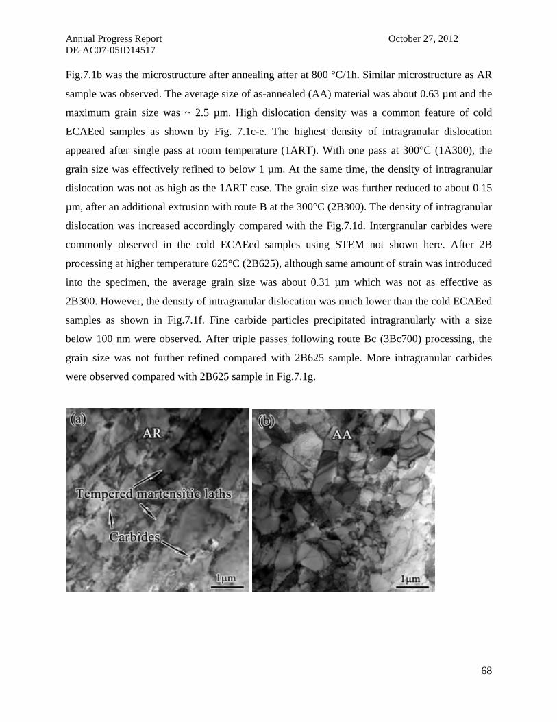
Annual Progress Report October 27, 2012 DE-AC07-05ID14517
68
Fig.7.1b was the microstructure after annealing after at 800 °C/1h. Similar microstructure as AR
sample was observed. The average size of as-annealed (AA) material was about 0.63 µm and the
maximum grain size was ~ 2.5 µm. High dislocation density was a common feature of cold
ECAEed samples as shown by Fig. 7.1c-e. The highest density of intragranular dislocation
appeared after single pass at room temperature (1ART). With one pass at 300°C (1A300), the
grain size was effectively refined to below 1 µm. At the same time, the density of intragranular
dislocation was not as high as the 1ART case. The grain size was further reduced to about 0.15
µm, after an additional extrusion with route B at the 300°C (2B300). The density of intragranular
dislocation was increased accordingly compared with the Fig.7.1d. Intergranular carbides were
commonly observed in the cold ECAEed samples using STEM not shown here. After 2B
processing at higher temperature 625°C (2B625), although same amount of strain was introduced
into the specimen, the average grain size was about 0.31 µm which was not as effective as
2B300. However, the density of intragranular dislocation was much lower than the cold ECAEed
samples as shown in Fig.7.1f. Fine carbide particles precipitated intragranularly with a size
below 100 nm were observed. After triple passes following route Bc (3Bc700) processing, the
grain size was not further refined compared with 2B625 sample. More intragranular carbides
were observed compared with 2B625 sample in Fig.7.1g.

Annual Progress Report October 27, 2012 DE-AC07-05ID14517
69
Fig. 7.1. TEM micrographs show the evolution of T91 steel. (a) As-received material contained fragment of the original martensitic laths in the ferritic matrix with carbides.(b) As-annealed material had similar microstructure with an average grain size d of 0.63 µm. (c) 1ART led to high density of dislocations. (d) 1A300 increased the density of dislocation further, and d became 0.27 µm. (e) 2B300 reduced d to 0.15 µm. (f) 2B625 had d of 0.31 µm and dislocation density inside the grains was lower than those processed at lower temperatures. (g) d in 3Bc700 specimen became 0.30 µm with relatively low density of dislocations. Numerous carbides were observed as well.

Annual Progress Report October 27, 2012 DE-AC07-05ID14517
70
Fig. 7.2. Typical bright field TEM micrographs with the SAD patterns show the grain boundary angle information of the initial and ECAE processed T91 steels (a) AR material, the zone axis is

Annual Progress Report October 27, 2012 DE-AC07-05ID14517
71
[311], low angle grain boundaries were detected between the four laths. (b) AA material, the
zone axis is [135 ], the grain boundary angle was about 5° as marked by arrows. (c) 1ART, the grain boundary angle was increased and some high angle grain boundaries were detected. (d) 1A300, the axis is again [311], all the grain boundaries detected were below 10°. (e) 2B300, high angle grain boundaries were detected hinted by the ring like diffraction pattern. (f) 2B625, high angle grain boundaries were observed and the small dots marked by the arrow were from the carbides at zone axis [011]. (g) 3Bc700, the grain boundaries were detected as predominately high angle grain boundaries.
The grain boundaries angle evolution is shown in Fig.7.2. Both AA and AR samples
showed predominately low angle grain boundaries as indicated by the inserted SAD patterns in
Fig. 7.2a-b. Grain boundary angle increased after 1A300, but still within the range of low angle
grain boundary as shown in Fig.7.2d. Meanwhile, 1ART resulted in high angle grain boundaries
according to Fig.7.2c. High angle grain boundaries were frequently observed after two or more
passes, as shown in Fig. 7.2e-g. In addition, one carbide particle was indexed as [011] zone axis
according to the diffraction pattern in Fig. 7.2f. The characteristic carbides showed an FCC
structure of M23C6 (M=Fe, Cr, Mo) with lattice parameter around 1.06 nm.
Fig.7.3 show the representative TEM micrographs of the T91 steel after heat treatment
(500°C/10h annealing). The AA samples showed more carbides precipitated along the prior
austenite and lath boundaries in Fig.7.3a. The prior austenite grain size was estimated about
20µm from the AA sample before heat treatment using a SEM image (not shown here). The
ECAE processed materials after heat treatment showed coarsened carbides. The density of
intragranular dislocation was significantly reduced in the cold ECAEed samples (1ART, 1A300
and 2B300) as shown in Fig. 7.3b-d. 1ART sample showed the largest carbides size as the high
dislocation density could accelerate the formation of carbides. The carbides in 2B625 or 3Bc700
samples also coarsened.

Annual Progress Report October 27, 2012 DE-AC07-05ID14517
72

Annual Progress Report October 27, 2012 DE-AC07-05ID14517
73
Fig. 7.3. TEM micrographs of T91 after heat treatment, 500°C/10h followed by furnace cooling.
For most specimens, (a-f), annealing induced an increase in the size and density of carbides and a
reduction of dislocation density. The average grain size was less influenced by annealing. In AA
specimen (a), more carbide particles were observed along the prior austenite grain boundaries
and the lath boundaries.
Statistical analyses of the microstructure results were performed to determine the size
distribution of grains and carbide particles. Fig.7.4a show the grain size distribution determined
from TEM micrographs by using linear intercept method (≥400 grains were analyzed for each
case). Grains as large as 2.7 µm existed in the AA alloy. Processing via route 1A300 refined the
maximum grain size to less than 1 µm. 2B300 resulted in further grain refinement to 0.6 µm with
high frequency of smaller grains. Hot ECAE processing (2B625 and 3B700) was less effective
compared with cold ECAE processing in the terms of grain refinement. The refinement of
carbides by ECAE was also noticed from Fig.7.4b ( ≥150 particles were analyzed for each case).
The refinement of carbides was not significantly by cold ECAE (1ART, 1A300, 2B300). On the
other hand, 2B625 refined the carbides size to less than 250 nm. 3Bc700 can further refine the
carbides to less than 100 nm. Hot ECAE seems more effective compared with cold ECAE in the
refining of carbides particles. After heat treatment (annealing at 500°C/10h), the carbides
coarsened slightly according to Fig.7.4c ( ≥170 particles were analyzed for each case). The
density of particle was also evaluated as shown in Fig.7.5. The thickness of the thin area in TEM
samples was assumed to be 100nm. Both the size and density showed strong correlation with the
processing temperature in Fig.7.5a. The carbides density increased six times after 3Bc700
processing compared with the AA condition. After heat treatment (500°C/10h), an increase of
density was noticed in AA and cold ECAEed samples, while a slightly decrease of density
occurred in the hot ECAEed samples as shown in Fig.7.5b.

Annual Progress Report October 27, 2012 DE-AC07-05ID14517
74
Fig. 7. 4. Grain and carbide size distributions in various T91 alloys. (a) Grain refinement
occurred in all ECAE processed specimens. 2B300 specimen showed the smallest average grain
size, about ~150nm. (b) 3Bc700 specimen had a large number of fine carbides with an average
diameter of 50nm. No significant refinement of carbides was observed in low temperature single
pass processing. 2B300 specimen showed slightly refinement of carbides. (c) After heat
treatment (500°C/10h), most carbides coarsened in the ECAE processed samples. HT:500°C
annealing 10h, furnace cooling
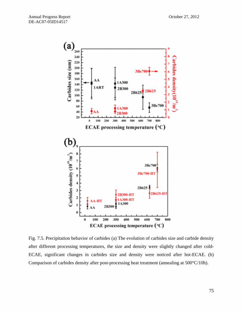
Annual Progress Report October 27, 2012 DE-AC07-05ID14517
75
Fig. 7.5. Precipitation behavior of carbides (a) The evolution of carbides size and carbide density
after different processing temperatures, the size and density were slightly changed after cold-
ECAE, significant changes in carbides size and density were noticed after hot-ECAE. (b)
Comparison of carbides density after post-processing heat treatment (annealing at 500°C/10h).

Annual Progress Report October 27, 2012 DE-AC07-05ID14517
76
7.2 Thermal stability and mechanical properties of ECAEed T91
Fig.7.6a and b show the hardness of the AA and ECAEed T91 alloys after 1h annealing
and 10h annealing at various temperatures up to 800°C. The AA sample showed good thermal
stability up to 700°C. For ECAE processed samples, the general grain coarsening started above
500°C, and significant softening occurred thereafter. The cold ECAEed samples soften after
300°C. After annealing at 700 or 800°C, the ECAE processed materials was even softer than the
AA material. After 10h annealing, the hardness of 2B625 sample slightly increased.
Fig. 7.6. Evolution of Vickers hardness after annealing for (a) 1 h and (b) 10 h. The recrystallization temperature is ~ 500°C. The ECAE processed samples were thermal stable up to 500°C/10h. Significant softening occurred above 500°C.

Annual Progress Report October 27, 2012 DE-AC07-05ID14517
77
Fig. 7.7. True stress-strain curves of T91 alloys. (a) After cold ECAE, specimens showed
significant increase in yield strength but considerable reduction of uniform elongation.
Specimens after hot ECAE exhibited moderate increase of yield strength but a retention of
ductility. (b) After annealing at 500°C/10h, specimens after cold ECAE showed significant
recovery of uniform elongation with insignificant loss of mechanical strength. Whereas the
increase of ductility for hot ECAE samples was less pronounced and an increase of tensile
strength was noticed. (c) Comparison of annealing effect on the tensile properties of cold ECAE
and hot ECAE samples.
HT:500°C annealing for 10h, furnace cooling

Annual Progress Report October 27, 2012 DE-AC07-05ID14517
78
Fig.7.7a provided a comparison of the tensile curves (true stress and true strain) of T91
alloys before and after ECAE. AA samples showed a slightly lower ultimate tensile strength
(σUTS) and yielding strength (σy) than AR samples with similar ductility. The 2B300 samples
showed the highest strength with σUTS and σy about 1031 and 982 MPa, respectively. The 3Bc700
samples exhibited the largest total elongation (ԑt=22%) and uniform strain (e=11%) among the
ECAEed samples. Fig.7.7b summarized the tensile curves of AA and ECAEed T91 steels after
annealing at 500°C for 10h. The ductility of cold ECAEed conditions (i.e.1ART, 1A300, and
2B300) improved significantly with slightly a little sacrifice of strength. By contrast, the ductility
of hot ECAEed cases (2B625, 3Bc700) remained the same, while a slight increase of strength
could be observed. After annealing, the 2B300 samples exhibit the highest strength
(σUTS=968MPa, σy=845MPa) with good ductility (ԑt=16%, e=6.5%). The 3Bc700 samples
exhibited the best ductility (ԑt=22%, e=11%) with good strength (σUTS=797MPa, σy=650MPa).
Fig.7.7c showed the typical annealing effect on the AA, cold ECAEed and hot ECAEed samples.
All the tensile test data have been collected in Table 3.
Table 7.3. Summary of the mechanical properties of the T91 steel subjected to various thermo-mechanical treatment conditions. The standard deviations are obtained from multiple independent experiments. Sample
ID
UTS(MPa) Yield strength
(MPa)
Elongation to
failure (%)
True uniform strain
(%)
Before
HT
After
HT
Before
HT
After
HT
Before
HT
After
HT
Before
HT
After HT
AR 681±4 - 508±1 - 20±2 - 10.6±1 -
AA 646±3 645±3 482±1 445±23 21±1 24±1 11.5±0.7 13.9±1.4
1ART 935±1 885±3 900±1 775±1 7.9±0.9 13±1 1.8±0.1 6.5±0.1
1A300 886±5 828±7 838±1 709±18 9.2±0.5 16±2 3±0.3 8.4±0.8
2B300 1031±1 968±3 982±1 845±15 8.5±0.1 16±2 1.8±0.1 6.5±0.7
2B625 805±2 848±22 681±16 719±13 10.9±1 13±1 5.3±0.8 5.2±0.2
3Bc700 763±15 797±23 615±3 650±3 22±2 22±1 11.1±1.6 11.1±0.8
HT:500°C annealing 10h, furnace cooling

Annual Progress Report October 27, 2012 DE-AC07-05ID14517
79
The microstructure evolution of ECAEed T91 steels
The grain refinement and evolution of grain boundary angle during ECAE was a
dislocation related process. The dislocation entangled and dislocation cells formed during
deformation. The size of the cell walls decreased with the increasing amount of strain. The cell
walls become sharper as the misorientation between two neighbor cells increased. Then the
subgrain boundaries formed through polygonization process.
The initial structure of tempered martensite laths within the same prior austenite grain
showed low angle grain boundaries in AA and AR samples. Similar results about grain
boundaries were observed by EBSD mapping of grade T91 during long time aging in early
observation. The grain size was about 3 µm. During ECAE, the density and distribution of
dislocation was strongly dependent on the temperature of deformation. Though same amount of
strain was applied, smaller grain size (~150nm) was formed during cold ECAE compared with
that of hot ECAE (~300nm), because the dislocation proliferated with slow recovery speed, so
the mean free path for dislocation interaction decreased. The 1ART sample showed higher
density of dislocation than the 1A300 sample, which can be also explained by the dynamic
recovery process during the deformation. The formation of low angle grain boundaries after
single pass was consistent with early observation in pure Al and Al alloys, because it was during
the beginning stage of dislocation interaction and the cell walls just formed, which was actually a
low angle grain boundary. After two passes, high angle grain boundaries begin to form. Three
passes following route Bc allowed the grain boundaries turned into predominated high angle
grain boundaries. Actually, route Bc was the most effective route to generate high angle grain
boundaries. The grain size of hot ECAE reached its refinement limited during 2B625 process,
because similar grain size was achieved through 3Bc700 process. The refining limited was
frequently observed in other metal and alloy systems during ECAE. The grain size and grain
angle evolution was estimated based on the transverse plane of the ECAE billets. Other
directions (such as flow plane and longitude plane) of observation may give total different
configuration. Because all the samples after ECAE processed were examined in the same plane,
the results were still comparable in the present case.
The precipitates behavior during ECAE and post-processing heat treatment
The processing of ECAE on grain refinement was well understood, but the behavior of
precipitates during ECAE was still open to question and less studied. No general conclusion was

Annual Progress Report October 27, 2012 DE-AC07-05ID14517
80
drawn from the existing results, because the precipitates behavior could be influenced by all the
thermomechanical history before or during ECAE, which was varied from case to case in
different systems. Previous results about precipitates hardening Al alloy showed the fracture of
precipitates, and a redistribution of the precipitates occurred, where the precipitates commonly
had a long plate or rod shape which exhibited a large stress concentrator. Study about Al based
metal matrix composites showed no or limited broken Al2O3 particles were observed. The high
processing temperature was supposed to be the drawback for breaking the particles. However,
there is a difference between the two kind of materials during ECAE deformation, because the
ceramic particles in metal matrix composites commonly show little solid solution into the matrix,
while precipitate hardening phases which were from the matrix can be resolved at elevated
temperature. The carbides precipitated behavior during ECAE in the present T91 alloy was
strongly dependent on the ECEA temperature. During the cold ECAE, the particles were almost
the same size and density as the AA condition. The carbide particles mostly belong to the
intergranular precipitates which located at the grain boundaries where the atoms were loosely
packed. During the hot ECAE, the carbide particles exhibited a small size with high density,
most of which belonged to the intragranular precipitates. Neither case showed broken particles.
The mechanism of the particles refinement was proposed in Fig.7.8 (Use 300°C and
700°C as examples for cold and hot ECAE). As the Fig. 7.8a-d illustrated, during the cold
ECAE, little solid solubility change to the elements consisted of carbides particles and prior
austenite grain boundaries during the temperature range of processing. During the deformation,
the particles have additional freedom at the grain boundaries, and the compression stress from
the soft matrix could not break the hard particles. Rotation of the particles could happen due to
the discontinuous of elastic and plastic properties at the interface between particles and matrix.
Finally, the prior austenite grain boundaries were mechanically broken but chemically
(segregation) and topologically (total length) conserved shown in Fig.7.8c. Actually, in Fig.7.2c,
the grain boundaries beside a carbide particle were curved by it during the deformation. Based on
the above explanation, no significant change of size or density should be expected at the
beginning stage of deformation (at least first pass). This property allowed the use of the carbides
as markers to observe the deformation behavior of prior-austenite grain boundaries. An example
of using precipitates as a marker to observe the material flow during ECAE was reported in the
reference. After annealing (500°C/10h), the size and distribution of carbide particles were

Annual Progress Report October 27, 2012 DE-AC07-05ID14517
81
changed again. The prior austenite grain boundaries were chemically and energetically favored
for the nucleation and growth of carbides. The coarsening of the precipitates could explain as the
pipe diffusion of alloying elements along dislocation cores during the aging process. The 1ART
showed the largest carbides after annealing because the highest dislocation density it possessed.
The newly formed grain boundaries could also serve as a nucleation sites for carbides particles.
Therefore, the density of carbides slightly increased.
During the hot ECAE as shown in Fig. 7.8a and e-g, solid solution process happened to
the element consisting the carbon particles and prior austenite grain boundaries. So the carbides
at triple junction or grain boundaries became smaller because they are high diffusion path shown
in Fig.7.8d. The segregation of elements at prior austenite grain boundaries begin to decrease
(shown in Fig.7.8d expressed as the thickness of the line decreased). The extrusion broke the
prior austenite grain boundaries. Repeated two or three times, the prior austenite grain
Fig. 7.8. Illustration of precipitates behavior during cold ECAE (a-b-c-d) and hot ECAE (a-e-f-g). Prior austenite grain boundary was the preference nucleation sites for carbides. The prior austenite grain boundaries were topologically and chemical conserved during cold ECAE (total length or composition was not significantly changed). The prior austenite grain boundaries were chemically eliminated during hot ECAE, so the carbides begin to precipitates randomly around the grain boundaries where the carbon concentration was slightly higher. After annealing around Tr (recrystallizaiton temperature), the dislocation density decreased and new carbides precipitates around prior austenite grain boundaries for cold ECAEed samples as shown in (d). Existing carbides begin to coarsen. For hot ECAEed samples, the carbides grew toward grain boundaries (g).
Annual Progress Report October 27, 2012 DE-AC07-05ID14517
82
boundaries were chemically eliminated, where commonly served as a preference nucleation sites
for carbides. New carbides could be precipitated in the random place due to the lost of preference
nucleation sites, commonly near the grain boundaries because the carbides dissolved there and
the carbon concentration was higher. So the carbides included the intragranular carbides which
was not dissolved and newly formed carbides during cooling process. The size of both particles
was influenced by the solid solubility of the alloying elements which was influence by the
processing temperature. The high temperature led to high solid solution, thus smaller
intragranular particles undissolved. This could explain the smaller size of particles was achieved
during hot ECAE. After annealing (500°C/10h), some of the carbides grew toward grain
boundaries during the annealing. Some intergranular particles also grew. The coherence was lost
during the annealing process. Some small particles probably dissolved due to Ostwald
coarsening process. A slightly decrease in density was observed in hot ECAE samples. If the
annealing time was long enough, both precipitates in hot ECAE and cold ECAE would reach the
equilibrium amount of precipitates.
Our discussion was based on the transverse plan of the billet processed by route B (with
three passes). The texture was not considered in the schematic. However, different route could
have different efficiency to break the prior austenite grain boundaries, thus the behavior of
precipitates probably show slightly difference. For more passes during cold ECAE, the size and
density of precipitates could also decreased because further deformation may lead to stress
assisted solid solution, which was frequently observed in mechanical alloying process. The size
was slightly refined and density decrease in 2B300 samples showed the trend consistent with this
argument.
The strengthening mechanism
The increase of the strength of ECAEed T91 alloys could come from the grain
refinement, the increasing density of dislocation and precipitates hardening. An established
strengthening model for grain refinement of pure metals or consolidated bulk metals (which
considered the strengthening from dislocation density and grain refinement) was proposed as
following[36]:
0y d (1),

Annual Progress Report October 27, 2012 DE-AC07-05ID14517
83
where σy is the yielding strength, σ0 is the lattice friction, the second term are due to the Taylor’s
equation, and the third term arises from the Hall-Petch relationship.
Considering the Orowan mechanism,
GbL
(2),
where σ is the additional strength needed due to the dislocation bypass an obstacle, L is the inter
particle distance on the slipping plane, which could relate to the particle density,
31L
n (3),
where n is the density of the particles.
The strengthening in the present study could be written as:
320 1 3y
kk Gb k Gb nd
(4),
where σy is the yielding strength, σ0 is the lattice friction, ρ is the dislocation density, d is the
average grain size, b is the burger’s vector, G is the shear modulus, n is the density of particles.
k1, k2, k3 are dependent on the material properties. k1 describes an average interaction strength
between dislocation. k2 is the grain boundary strengthen which was a function of grain
boundaries properties such as grain boundaries angles. k3 is related to the efficiency of
precipitates as an obstacle to block dislocations. The above equation is the simplest scenario
where simple rule of mixture is applied. A more accurate description of Taylor’s equation and
strain hardening was described in the literature.
The AA samples showed the lowest yielding strength, because the grain size was large
and dislocation density was low. The precipitates located at grain boundaries which showed low
efficiency to block the mobile dislocation. After cold ECAE, the dislocation density ρ was
significantly increased and the grain size d decreased, thus an enhancement in strength should be
expected. However, due to the low dislocation accumulation capability, the samples after cold
ECAE commonly showed low or no work hardening rate. Although some research showed that
after more passes the ductility could increase a few percent, that probably due to the increase
fraction of high angle grain boundaries, which change the dislocation movement mechanism to
grain boundaries sliding or rotation. The samples after hot ECAE exhibited a small dislocation
density ρ with decreased grain size d. The precipitates were located within the grain with a very

Annual Progress Report October 27, 2012 DE-AC07-05ID14517
84
high density. The strengthening also occurred. The samples after hot ECAE commonly exhibited
good work hardening rate due to the low density of dislocation after processing.
After annealing, cold ECAE samples showed decreased of strengthen and increase of
ductility due to decrease of dislocation density during recovery process. The ductility of hot
ECAE samples remained the same while a slightly increase of strength were noticed. Just like the
beginning stage of aging hardening Al alloys, the rearrange of solute atoms in the matrix should
have some influence in the friction strength σ0. Moreover, the grain boundaries angle change
(related to the k2 term in the equation) could influence the strengthen. The low angle grain
boundary was proved to be lower efficiency in the dislocation pile-ups mechanism than the high
angle grain boundaries.
A8. Grain boundary engineering on ECAP processed specimen
Lead organization: University of Florida (Yong Yang) and
University of Wisconsin, Madison (Todd Allen)
8.1 Overview
The grain structures of ECAPed model alloy, 304L and 316L Stainless steels were characterized
using Electron Backscatter Diffraction (EBSD) technology, the average grain size, grain size
distribution, and phases were fully studied. Moreover, the nanoMegas was used to study the
nano-sized grains under TEM, and the system is equipped on JEOL 2010F TEM. Figure 3.2.1
shows a basic set up of the system, which consists of beam scanning unit, high speed external
optical CCD camera and image processing, and automated indexing module. The acquired
diffraction patterns are matched again pre-calculated solutions of crystal orientation. The
selected materials were also studied using Transmission Electron Microscopy (TEM), and the
samples were prepared using an electro-polishing method (Single Jet Polish, Southbay
Technology, CA).
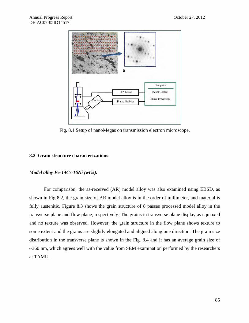
Annual Progress Report October 27, 2012 DE-AC07-05ID14517
85
Fig. 8.1 Setup of nanoMegas on transmission electron microscope.
8.2 Grain structure characterizations:
Model alloy Fe-14Cr-16Ni (wt%):
For comparison, the as-received (AR) model alloy was also examined using EBSD, as
shown in Fig 8.2, the grain size of AR model alloy is in the order of millimeter, and material is
fully austenitic. Figure 8.3 shows the grain structure of 8 passes processed model alloy in the
transverse plane and flow plane, respectively. The grains in transverse plane display as equiaxed
and no texture was observed. However, the grain structure in the flow plane shows texture to
some extent and the grains are slightly elongated and aligned along one direction. The grain size
distribution in the transverse plane is shown in the Fig. 8.4 and it has an average grain size of
~360 nm, which agrees well with the value from SEM examination performed by the researchers
at TAMU.

Annual Progress Report October 27, 2012 DE-AC07-05ID14517
86
Fig 8.2 Inverse Pole Figure (IPF) of as-received model alloy.
(a) (b)
Fig 8.3 IPF image of ECAPed Model Alloy (8 passes, 500 ºC): (a) transverse plane; (b) flow
plane.
Fig. 8.4 Grain size distribution in
the transverse plane of ECAPed
Model alloy (8 passes, 500 ºC)
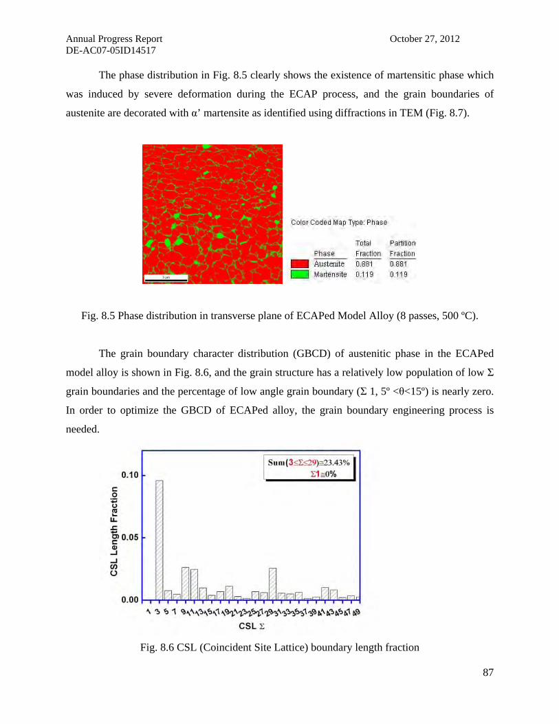
Annual Progress Report October 27, 2012 DE-AC07-05ID14517
87
The phase distribution in Fig. 8.5 clearly shows the existence of martensitic phase which
was induced by severe deformation during the ECAP process, and the grain boundaries of
austenite are decorated with α’ martensite as identified using diffractions in TEM (Fig. 8.7).
Fig. 8.5 Phase distribution in transverse plane of ECAPed Model Alloy (8 passes, 500 ºC).
The grain boundary character distribution (GBCD) of austenitic phase in the ECAPed
model alloy is shown in Fig. 8.6, and the grain structure has a relatively low population of low Σ
grain boundaries and the percentage of low angle grain boundary (Σ 1, 5º <θ<15º) is nearly zero.
In order to optimize the GBCD of ECAPed alloy, the grain boundary engineering process is
needed.
Fig. 8.6 CSL (Coincident Site Lattice) boundary length fraction
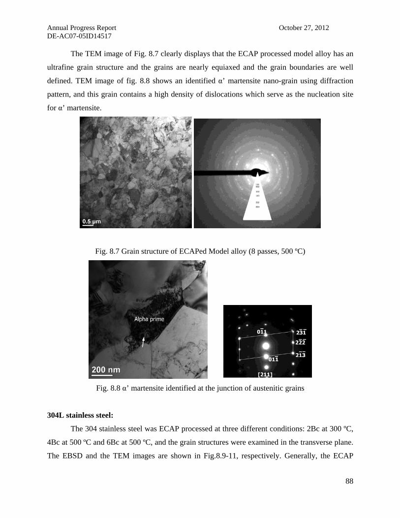
Annual Progress Report October 27, 2012 DE-AC07-05ID14517
88
The TEM image of Fig. 8.7 clearly displays that the ECAP processed model alloy has an
ultrafine grain structure and the grains are nearly equiaxed and the grain boundaries are well
defined. TEM image of fig. 8.8 shows an identified α’ martensite nano-grain using diffraction
pattern, and this grain contains a high density of dislocations which serve as the nucleation site
for α’ martensite.
Fig. 8.7 Grain structure of ECAPed Model alloy (8 passes, 500 ºC)
Fig. 8.8 α’ martensite identified at the junction of austenitic grains
304L stainless steel:
The 304 stainless steel was ECAP processed at three different conditions: 2Bc at 300 ºC,
4Bc at 500 ºC and 6Bc at 500 ºC, and the grain structures were examined in the transverse plane.
The EBSD and the TEM images are shown in Fig.8.9-11, respectively. Generally, the ECAP
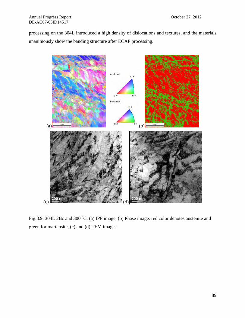
Annual Progress Report October 27, 2012 DE-AC07-05ID14517
89
processing on the 304L introduced a high density of dislocations and textures, and the materials
unanimously show the banding structure after ECAP processing.
(a) (b)
(c) (d)
Fig.8.9. 304L 2Bc and 300 ºC: (a) IPF image, (b) Phase image: red color denotes austenite and
green for martensite, (c) and (d) TEM images.

Annual Progress Report October 27, 2012 DE-AC07-05ID14517
90
(a) (b)
(c) (d)
Fig.8.10. 304L 4Bc and 500 ºC: (a) IPF image, (b) Phase image: red color denotes austenite and
green for martensite, (c) and (d) TEM images.
(a) (b)

Annual Progress Report October 27, 2012 DE-AC07-05ID14517
91
(c) (d)
Fig. 8.11 304L 6Bc and 500 ºC: (a) IPF image, (b) Phase image: red color denotes austenite and green for martensite, (c) and (d) TEM images.
316L stainless steel:
The 316L stainless steel was also ECAP processed at conditions of 2 Bc at 300 ºC and 4
Bc at 500 ºC. And compared with 304L SS, the 316L SS shows more degraded microstructures
regarding to the grain refining, uniformity of grain size, and phase transformation after ECAP
processing. The microstructures of processed 316L SS are shown in Fig. 8.12-13. Due to the
high density of dislocation density, the EBSD patterns were smeared and the image quality was
significantly degraded. TEM images show that the shear bands are the typical microstructural
features of the processed materials and the deformation twins were widely observed in the parent
austenite after deformation. The martensites might be a mixture of ε phase and α’ phase while
more TEM studies are needed.
(a) (b)
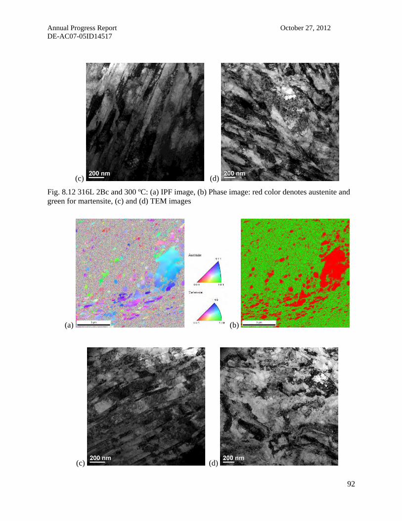
Annual Progress Report October 27, 2012 DE-AC07-05ID14517
92
(c) (d)
Fig. 8.12 316L 2Bc and 300 ºC: (a) IPF image, (b) Phase image: red color denotes austenite and green for martensite, (c) and (d) TEM images
(a) (b)
(c) (d)

Annual Progress Report October 27, 2012 DE-AC07-05ID14517
93
Fig. 8.13. 316L 4Bc and 500 ºC: (a) IPF image, (b) Phase image: red color denotes austenite and green for martensite, (c) and (d) TEM images
Ferrite content
EBSD, TEM and X-ray diffraction all show the existence of ferrite phase (martensite)
which is derived from deformed fcc crystal structure under the high shear loading. The content of
selected specimen were characterized using a ferrite scope. Figure 8.14 shows the summary of
ferrite contents in the as-received, 500°C/8 passes and 300°C/4Bc processed model alloy,
respectively. And for each sample, twenty measurements were performed. It clearly shows that
larger number of pass will definitely introduce a higher percentage of ferritic/martensitic phase
even though the processing temperature is higher.
Figure 8.14. Ferrite (Martensitic) percentages measured using a ferrite scope.
Summary
As compared with 304L and 316L, the model alloy shows the most desired grain
structures after ECAP processing. The refined grain structures are determined by both the
composition and the grain size of parent austenite. And the transformation sequence of γ→ε→α’
needs to be studied more systematically by examining the materials processed at a series of
number of passes, which can be helpful for minimizing the volume of α’ phase.

Annual Progress Report October 27, 2012 DE-AC07-05ID14517
94
8.3 Grain boundary engineering on ECAPed model alloy
The GBE parameters were originally selected based the reported GBE research on the
316 and 304 stainless steels, and in order to screen the parameters, a test matrix was conducted
as listed in the table 3.1. The cold work percentages of 0, 5 and 10% were applied on the 1.5 mm
thick flat coupons and then subjected to thermal annealing at 1027 ºC for 2, 5 and 10 minutes,
respectively. The grain structures were examined using EBSD, and the characterizations were
firstly performed on the 5% cold rolled specimen since the 5% cold work was widely reported as
an optimal thickness reduction rate for GBE on the austenitic steels.
Table 8.1. Grain boundary engineering test matrix (annealing at 1027 ºC).
Cold work (%)
Annealing
time (mins)
0 5 10
2 x x x
5 x x x
10 x x x
However, as shown previously, the ECAPed specimen has a poor thermal stability at this
annealing temperature, and a significant coarsening behavior of the grains was observed. It can
be seen that for the 5% cold worked specimen, the nanocrystalline structure readily evolved into
a micro-sized grain structure even after 2 mins thermal annealing. The EBSD characterization
was not conducted for the other two cold work conditions since this annealing temperature was
obviously too high. The significant coarsening behavior can be caused by a lowed
recrystallization temperature from ECAP process, and additionally the very low carbon content
and no carbide precipitates in the model alloy can further deteriorate the grain boundary stability
since there is lack of a pinning mechanism at GBs and they can migrate relatively freely. The
phase image of Fig.8.16 shows that all the ECAP induced martensitic phase already dissolved
after 2 min annealing.

Annual Progress Report October 27, 2012 DE-AC07-05ID14517
95
Based on previous furnace annealing experiments and the in-situ TEM heating
experiments, the temperature of 700ºC tends to be better choice for the GBE processing
temperature. And the ECAPed model alloy was annealed for 5, 20 and 60 minutes at 700 ºC,
respectively; the annealing was conducted in a box furnace and the samples were water quenched
after annealing. The annealed samples were then studied using EBSD and TEM for grain
boundary character distribution, grain coarsening and the evolution of dislocation structures.
Figure 8.17 shows that the fraction of CSL boundaries changes vs. the annealing time, and the 5
minutes annealing gives the highest portion of Σ3 as well as the fraction of 1≤Σ3≤29 boundaries.
Figure 8.18 displays the distributions of grain size of the samples after three different annealing
periods, and it can be seen that the grain size averagely increases to 2.58µm after 5 minutes,
while there a very small difference in the grain size between the 20 minutes and 60 minutes
annealed specimens as shown in Fig. 8.19. And it should be noted that the annealing at shorter
time tends to introduce a binominal distribution of grain size while the longer time annealing
promotes a normal distribution of grain size These results demonstrate that a very short time
annealing at high temperature can effectively increase the fraction of Σ grain boundary while has
a least coarsening effect on the grain size.
Figure 8.15 Grain coarsening after various annealing periods at 1027 ºC for 5% cold rolled
ECAPed model alloy.

Annual Progress Report October 27, 2012 DE-AC07-05ID14517
96
Figure 8.16. Phase image of the 2 mins annealed (1027 ºC) ECAP specimen.
Figure 8.17 Fraction of CSL boundaries vs. the annealing time.

Annual Progress Report October 27, 2012 DE-AC07-05ID14517
97
Figure 8.18 Grain size distribution vs. the annealing time.
(a) (b) (c)
Figure 8.19. OIM image of the annealed (700 ºC) specimen (a) 5 min, (b) 20 min and (c) 60 min.
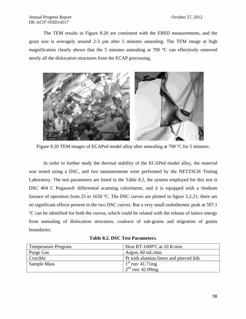
Annual Progress Report October 27, 2012 DE-AC07-05ID14517
98
The TEM results in Figure 8.20 are consistent with the EBSD measurements, and the
grain size is averagely around 2-3 µm after 5 minutes annealing. The TEM image at high
magnification clearly shows that the 5 minutes annealing at 700 ºC can effectively removed
nearly all the dislocation structures from the ECAP processing,
Figure 8.20 TEM images of ECAPed model alloy after annealing at 700 ºC for 5 minutes.
In order to further study the thermal stability of the ECAPed model alloy, the material
was tested using a DSC, and two measurements were performed by the NETZSCH Testing
Laboratory. The test parameters are listed in the Table 8.2, the system employed for this test is
DSC 404 C Pegasus® differential scanning calorimeter, and it is equipped with a rhodium
furnace of operation from 25 to 1650 ºC. The DSC curves are plotted in figure 3.2.21; there are
no significant effects present in the two DSC curves. But a very small endothermic peak at 597.1
ºC can be identified for both the curves, which could be related with the release of lattice energy
from annealing of dislocation structures, coalesce of sub-grains and migration of grains
boundaries.
Table 8.2. DSC Test Parameters.
Temperature Program Heat RT-1000ºC at 10 K/min Purge Gas Argon, 60 mL/min Crucible Pt with alumina liners and pierced lids Sample Mass 1st run: 41.71mg
2nd run: 42.09mg

Annual Progress Report October 27, 2012 DE-AC07-05ID14517
99
Figure 8.21 DSC curves for two ECAPed sample test from 25 to 1000 ºC.
A9. In situ Kr ion irradiation of ECAPed Fe-14Cr-16Ni
Lead organization: University of Florida (Yong Yang) and University of Wisconsin,
Madison (Todd Allen)
9.1 In-situ irradiation and characterizations
The ion irradiation experiments were performed using the in-situ ion beam at the
Argonne National Laboratory. And the planned irradiation conditions are listed in the Table 9.1
with the completed conditions shadowed, where the ECAP+HT denotes the heat treated
ECAPped specimen, and heat treatment condition is: annealing at 700 °C for 5 min followed by
water quenching. For each temperature condition, the irradiations were terminated at 2, 5 and 10
dpa, respectively, so the irradiated specimens can be re-examined after in-situ experiment.
However, the irradiation at 500 °C was only performed at the dose up to 2 dpa due to the
excessively receding of the electron transparent area during experiment, which can be caused by
the surface diffusion at this temperature in a high vacuum. And due to a very limited access to
the equipment, only partial of the experiments was completed.
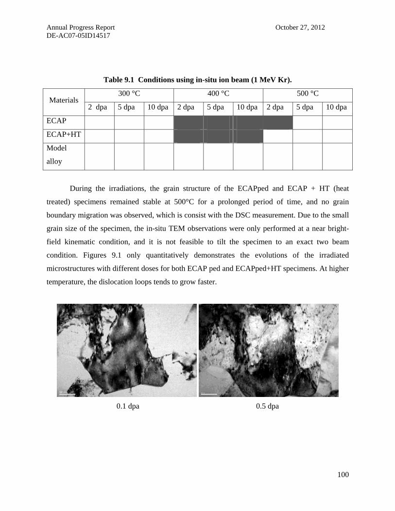
Annual Progress Report October 27, 2012 DE-AC07-05ID14517
100
Table 9.1 Conditions using in-situ ion beam (1 MeV Kr).
Materials 300 °C 400 °C 500 °C
2 dpa 5 dpa 10 dpa 2 dpa 5 dpa 10 dpa 2 dpa 5 dpa 10 dpa
ECAP
ECAP+HT
Model
alloy
During the irradiations, the grain structure of the ECAPped and ECAP + HT (heat
treated) specimens remained stable at 500°C for a prolonged period of time, and no grain
boundary migration was observed, which is consist with the DSC measurement. Due to the small
grain size of the specimen, the in-situ TEM observations were only performed at a near bright-
field kinematic condition, and it is not feasible to tilt the specimen to an exact two beam
condition. Figures 9.1 only quantitatively demonstrates the evolutions of the irradiated
microstructures with different doses for both ECAP ped and ECAPped+HT specimens. At higher
temperature, the dislocation loops tends to grow faster.
0.1 dpa 0.5 dpa

Annual Progress Report October 27, 2012 DE-AC07-05ID14517
101
1 dpa 2 dpa
5 dpa
Fig. 9.1 Microstructural evolution in ECAP model alloy irradiated at 400 °C
0.1 dpa 0.2 dpa
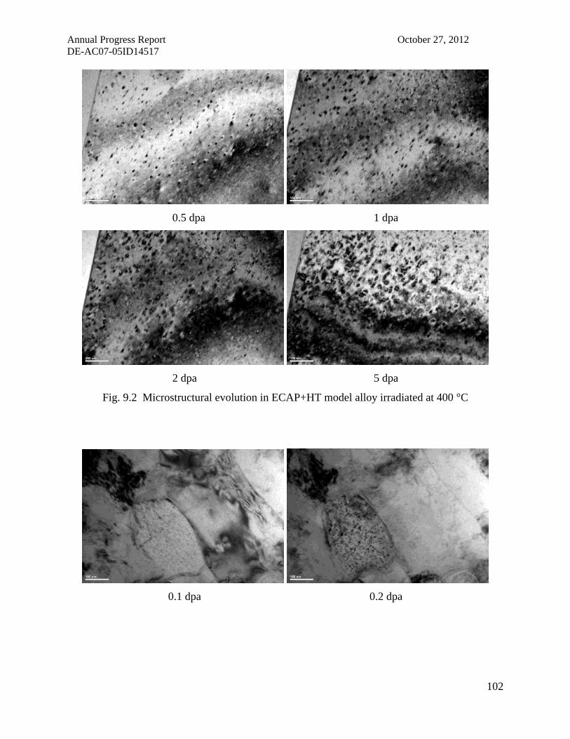
Annual Progress Report October 27, 2012 DE-AC07-05ID14517
102
0.5 dpa 1 dpa
2 dpa 5 dpa
Fig. 9.2 Microstructural evolution in ECAP+HT model alloy irradiated at 400 °C
0.1 dpa 0.2 dpa

Annual Progress Report October 27, 2012 DE-AC07-05ID14517
103
1 dpa 2 dpa
Fig. 9.3 Microstructural evolution in ECAP model alloy irradiated at 500 °C
As clearly shown in figure 9.3, the defect number tends to saturate even after only 1 dpa
while the size of dislocation loops is growing with an increasing ion fluence. Unfortunately, no
defect denude zones were observed near by the grain boundaries of the nano-sized grain (200nm)
as shown in figure 9.3 for even 500°C irradiation. The results clearly show that ~100-200nm
grain size would have a minimal effect on the point defects migration, and the spacing of grain
boundaries as defect sinks is much large than the diffusion length of point defects. In order to
improve the radiation damage resistance, a further refined grain structure is needed.
9.2 Fe2+ irradiation and characterization:
The ECAPed (8Bc, 500°C) model alloy was irradiated to 50dpa using a 5MeV F++ beam, as
shown in figure 9.4, the peak of radiation damage profile is about 1.5 m from the surface. The
TEM specimens prepared using a FIB lift-out methods as shown in Figure 9.5.

Annual Progress Report October 27, 2012 DE-AC07-05ID14517
104
Figure 9.4 SRIM calculation of the radiation damage file and implanted Fe in the 5MeV F++
irradiated ECAPed model alloy.
Figure 9.5 TEM specimen prepared using a FIB lift-out method
Microstructural examination:
As shown in Figure 9.6, the irradiated surface was well preserved by depositing a 100 nm
thick Pt by the lift out. Base on the SRIM calculation, the peak dpa is about 1.2 μm from the
surface, therefore the TEM should cover the whole irradiated zone in the irradiation direction.

Annual Progress Report October 27, 2012 DE-AC07-05ID14517
105
Figure 9.6 TEM image of Fe2+ irradiated ECAPed model alloy.
However, possible due to the saturation of defects, low irradiation temperature, and high
density of pre-existing dislocations, no clear radiation damage profile can be identified in this
irradiated sample. And the irradiated microstructure is generally decorated with a high density of
dislocation loops, as shown in Figure 9.7. The image was taken at the position about 1μm from
the irradiated surface. Additionally, no denude zones were identified nearby the grain boundary,
which might be because of the low irradiation temperature as well as the migration of grain
boundary during irradiation.
Figure 9.7. Dislocation loops and grain boundaries in Fe++ irradiated ECAPed model alloy.

Annual Progress Report October 27, 2012 DE-AC07-05ID14517
106
Nevertheless, the grain growth in irradiated zone is observable and the growth behavior is
abnormal with some large grains emerging while some very fine grains still remains intact even
after irradiation of 50dpa.
NanoMegas characterization
The grain growth of 1 MeV Kr irradiated ECAPed model alloy was quantified using
nanoMegas equipped on JEOL 2010F TEM. The TEM specimen was previously irradiated to
5dpa at 300°C using Kr ions, and the TEM image of figure 9.8 shows a high density of
dislocation loops in the irradiated microstructure. And this high density of dislocation loops
makes the measurement of grain size and boundary type impossible by using the conventional
Kikuchi pattern based EBSD technique, because high density of dislocation loops severely
distorts the lattices and smears out the Kikuchi pattern.
Figure 9.8 TEM image of Kr irradiated ECAPed model alloy.
By using NanoMegas system, the grain images were acquired with a step size of 10nm
and scanned area of 2000×2000nm2, the austenite and martensite phases were fitted over the
acquired data. Figure 9.9 shows the inverse pole image, quality map, combined quality and
orientation map and phase map, respectively. It can be seen that the size of grain slightly
increased after irradiation, and similar with the response to Fe2+ irradiation, the growth of grain
is abnormal. The martensite phase identified at the triple grain boundary junction remains

Annual Progress Report October 27, 2012 DE-AC07-05ID14517
107
nanoscale, which might be attributed to a more stable phase boundaries as compared with the
dislocation boundaries in the nanoscale austenitic phase after ECAP processing.
(a) (b)
(c) (d)
Figure 9.9. Grains of Kr irradiated ECAPed model alloy: (a) inverse pole map, (b) image quality
map, (c) combined orientation and quality image and (d) phase map (red as austenite and blue as
martensite).
Atom Probe Tomography
The Atom Probe Tomography (APT) was also applied on the ECAPed model alloy to
reveal any elemental segregation along dislocation lines or grain boundaries as well as to identify
any fine precipitates from the ECAP processing. Totally, seven APT tips were lifted out for the
electropolished specimen using FIB, and the APT was run on an IMAGO Leap at CAF-UA.
Figure 9.10 shows an example of the APT images of the ECAPed model alloy tip; it shows that
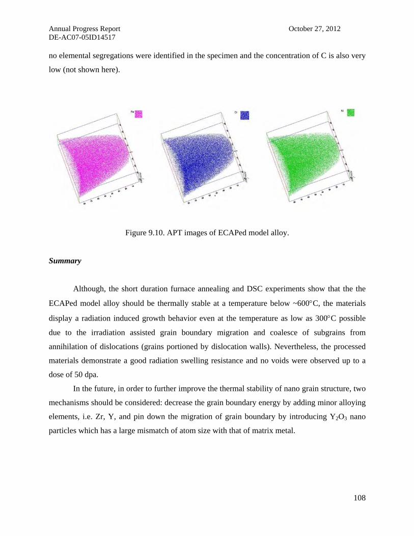
Annual Progress Report October 27, 2012 DE-AC07-05ID14517
108
no elemental segregations were identified in the specimen and the concentration of C is also very
low (not shown here).
Figure 9.10. APT images of ECAPed model alloy.
Summary
Although, the short duration furnace annealing and DSC experiments show that the the
ECAPed model alloy should be thermally stable at a temperature below ~600C, the materials
display a radiation induced growth behavior even at the temperature as low as 300C possible
due to the irradiation assisted grain boundary migration and coalesce of subgrains from
annihilation of dislocations (grains portioned by dislocation walls). Nevertheless, the processed
materials demonstrate a good radiation swelling resistance and no voids were observed up to a
dose of 50 dpa.
In the future, in order to further improve the thermal stability of nano grain structure, two
mechanisms should be considered: decrease the grain boundary energy by adding minor alloying
elements, i.e. Zr, Y, and pin down the migration of grain boundary by introducing Y2O3 nano
particles which has a large mismatch of atom size with that of matrix metal.

Annual Progress Report October 27, 2012 DE-AC07-05ID14517
109
A10. Mechanical properties of nanocrystalline 304L and 316L stainless steels processed by
ECAP. Lead organization (Texas A&M, Xinghang Zhang)
Processing
Commercial 304L and 316L stainless steel were used in this study. The starting material
for each is a long bar (rod) of pre-extruded material of an approximately one inch square cross
section from which the billets were cut. The cross-section of specimens was reduced accordingly
by milling in order to accommodate for thermal expansion of material. A nominal composition
for each is given in Table 10.1.
Table 10.1. Nominal composition of 304L and 316L SS.
Wt. % 304L 316L
Cr 18.19 15.94
Ni 8.04 10.13
Mn 1.68 1.38
Cu 0.55 -
Co 0.16 -
S 0.03 0.03
Si 0.3 0.47
N 0.08 0.77
P 0.026 0.028
Mo 0.12 2.01
C 0.02 0.028
Fe Balance Balance
There were different processing conditions for different specimens. Table 10.2 contains
the key details and identifiers that will be referenced throughout this report.
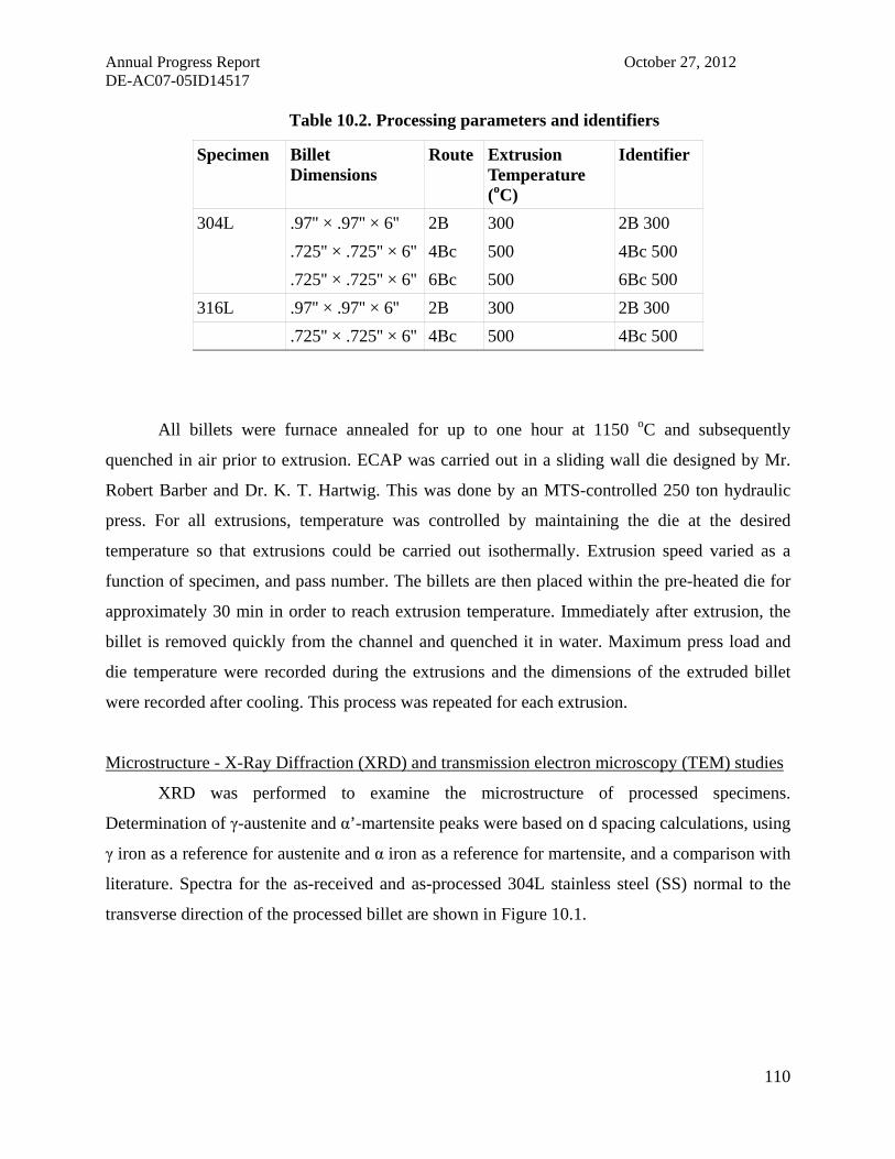
Annual Progress Report October 27, 2012 DE-AC07-05ID14517
110
Table 10.2. Processing parameters and identifiers
Specimen Billet Dimensions
Route Extrusion Temperature (oC)
Identifier
304L .97'' × .97'' × 6'' 2B 300 2B 300
.725'' × .725'' × 6'' 4Bc 500 4Bc 500
.725'' × .725'' × 6'' 6Bc 500 6Bc 500
316L .97'' × .97'' × 6'' 2B 300 2B 300
.725'' × .725'' × 6'' 4Bc 500 4Bc 500
All billets were furnace annealed for up to one hour at 1150 oC and subsequently
quenched in air prior to extrusion. ECAP was carried out in a sliding wall die designed by Mr.
Robert Barber and Dr. K. T. Hartwig. This was done by an MTS-controlled 250 ton hydraulic
press. For all extrusions, temperature was controlled by maintaining the die at the desired
temperature so that extrusions could be carried out isothermally. Extrusion speed varied as a
function of specimen, and pass number. The billets are then placed within the pre-heated die for
approximately 30 min in order to reach extrusion temperature. Immediately after extrusion, the
billet is removed quickly from the channel and quenched it in water. Maximum press load and
die temperature were recorded during the extrusions and the dimensions of the extruded billet
were recorded after cooling. This process was repeated for each extrusion.
Microstructure - X-Ray Diffraction (XRD) and transmission electron microscopy (TEM) studies
XRD was performed to examine the microstructure of processed specimens.
Determination of γ-austenite and α’-martensite peaks were based on d spacing calculations, using
γ iron as a reference for austenite and α iron as a reference for martensite, and a comparison with
literature. Spectra for the as-received and as-processed 304L stainless steel (SS) normal to the
transverse direction of the processed billet are shown in Figure 10.1.

Annual Progress Report October 27, 2012 DE-AC07-05ID14517
111
40 44 48 52 56 600
20000
40000
60000
80000
100000
Inte
nsity
(A
.U.)
2o
AR1A RT
2B 300
4Bc 500
6Bc 500
(111)
(200)' (110)
Fig. 10.1. 304L stainless steel XRD spectra for as-received and as-processed material.
The fully-annealed as-received (AR) specimen indicates a predominantly γ-austenite
phase. Subsequent processing at elevated temperatures (300oC or greater) seems also to preserve
the predominant γ-austenite with generation of a few stress-induced α'-martensite phases. The
story is significantly different for 304L SS processed at room-temperature. The spectrum shows
that α’-martensite dominates when processed at room temperature. This may explain the
difficulty in achieving more than one extrusion at this condition as significant hardening occurs
as shown later.
A similar situation arises in the 316L SS as shown in Fig. 10.2. Of worthy note is the fact
that stress-induced martensite seems to be significantly suppressed. As shown by the 1A RT
spectrum, unlike 304L 1A RT, a predominant γ-austenite is still preserved after room-
temperature processing. Indeed, α'-martensite formation is still suppressed even after higher-
temperature (300oC or greater) extrusions, and so does not appear in any significant quantity.
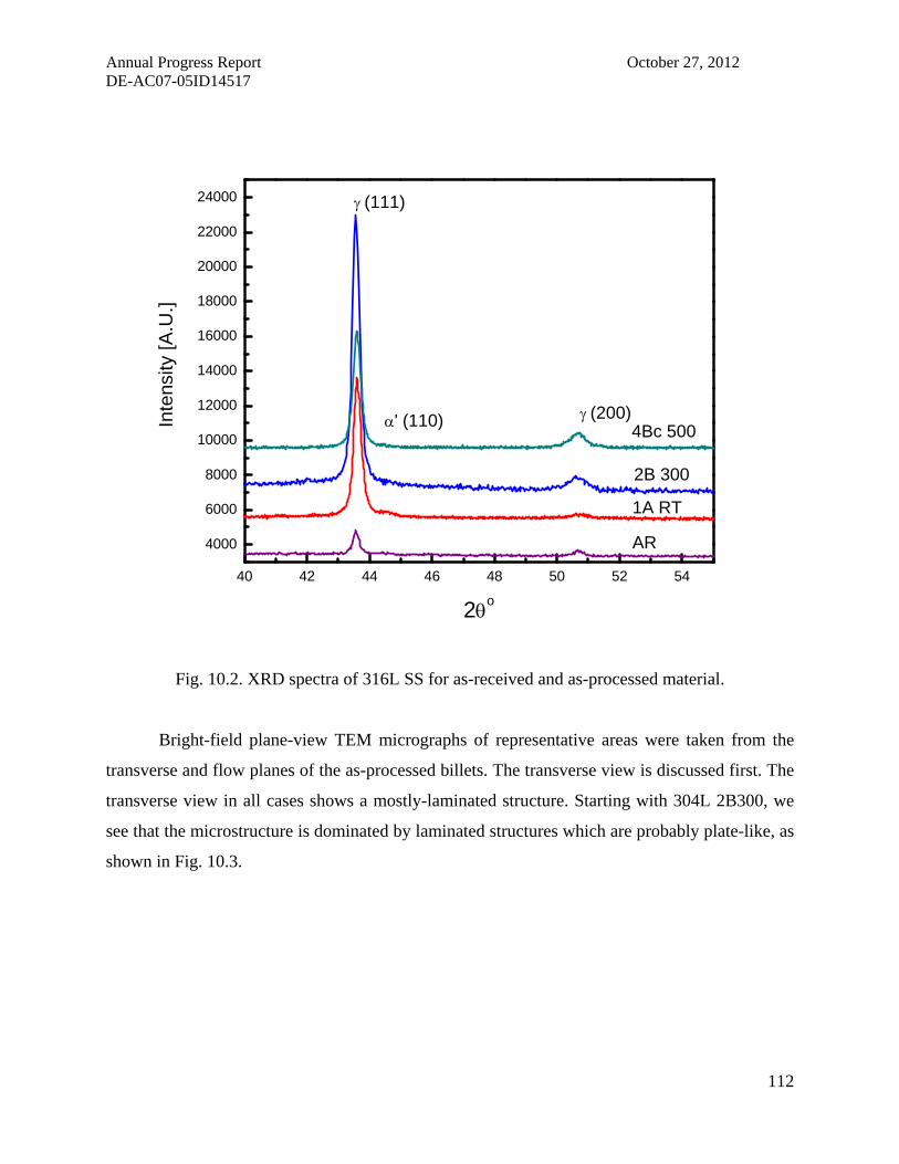
Annual Progress Report October 27, 2012 DE-AC07-05ID14517
112
40 42 44 46 48 50 52 54
4000
6000
8000
10000
12000
14000
16000
18000
20000
22000
24000
In
tens
ity [
A.U
.]
2o
AR
1A RT
2B 300
4Bc 500
(111)
(200)' (110)
Fig. 10.2. XRD spectra of 316L SS for as-received and as-processed material.
Bright-field plane-view TEM micrographs of representative areas were taken from the
transverse and flow planes of the as-processed billets. The transverse view is discussed first. The
transverse view in all cases shows a mostly-laminated structure. Starting with 304L 2B300, we
see that the microstructure is dominated by laminated structures which are probably plate-like, as
shown in Fig. 10.3.

Annual Progress Report October 27, 2012 DE-AC07-05ID14517
113
Fig. 10.3. (a) 304L 2B 300 bright field TEM micrograph showing laminated grains along
the transverse direction. Selected area diffraction pattern (SAD) (not shown here) shows
polycrystalline nature of grains with certain texture and predominant austenite structure.
Fig. 10.4. Frequency histogram of 304L 2B 300C specimen showing the unimodal character of
laminar thickness with an average laminar thickness of ~ 70 nm.
50 75 100 12502
468
1012
1416
1820
304L 2B300
D1 (nm)
Fre
quen
cy

Annual Progress Report October 27, 2012 DE-AC07-05ID14517
114
The laminar structures are highly anisotropic in dimensions indicated by the frequency
distribution for the grain size of the laminar spacing which shows an effectively unimodal
distribution which confirms a uniform structural refinement (Figure 10.4), with an average
thickness (D1) of ~ 70 nm. The length of laminations averages at ~ 1.8 μm. The continuous ring
in the selected area diffraction (SAD) pattern indicates a fine-grained polycrystalline
microstructure with certain texture. All the laminations or “columns” appear to be oriented the
same way as can be discerned by moving the viewing area around.
Further processing at higher temperature shows that the laminar structure remains, but the
length of grains decrease significantly as shown in Fig.10.5a for the 304L 4Bc 500 specimen.
The average laminar spacing increases slightly in order to accommodate the decrease in length.
Average laminar spacing (D1) becomes ~ 120 nm while the longer dimension (D2) has an
average length of ~250 nm with a bi-modal distribution, albeit with a noticeably smaller
occurrence of larger grains. Furthermore, some equiaxed grains become apparent. The bi-modal
distribution of D2 is indicative of the occurrence of grain columns being compressed as will be
more apparent in the case of the six-pass material.
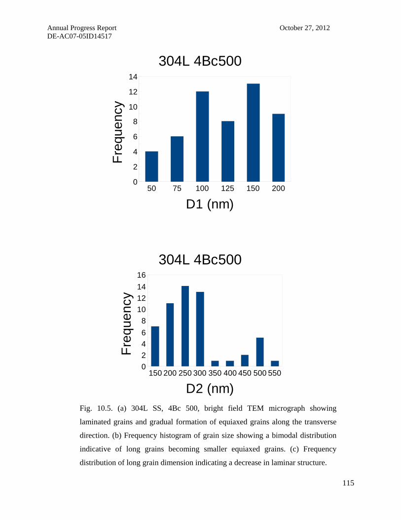
Annual Progress Report October 27, 2012 DE-AC07-05ID14517
115
50 75 100 125 150 2000
2
4
6
8
10
12
14
304L 4Bc500
D1 (nm)
Fre
quen
cy
150 200 250 300 350 400 450 500 5500
2
4
6
8
10
12
14
16
304L 4Bc500
D2 (nm)
Fre
quen
cy
Fig. 10.5. (a) 304L SS, 4Bc 500, bright field TEM micrograph showing
laminated grains and gradual formation of equiaxed grains along the transverse
direction. (b) Frequency histogram of grain size showing a bimodal distribution
indicative of long grains becoming smaller equiaxed grains. (c) Frequency
distribution of long grain dimension indicating a decrease in laminar structure.

Annual Progress Report October 27, 2012 DE-AC07-05ID14517
116
After six passes, the 304L 6Bc 500 sample undergoes even further grain refinement as is
evident in Fig. 10.6. The average laminar spacing now decreases slightly to ~ 100 nm, as shown
in Fig. 10.7a, and the size distribution takes on a more obvious unimodal characteristic which
also implies that the threshold for grain refinement is being reached. Similarly, the longer
dimension decreases further to an average size of ~ 260 nm, also with a unimodal type of
distribution as presented in Fig. 10.7b. Upon close examination of the micrograph, more
equiaxed grains can be discerned within the surrounding laminated grains. This is consistent with
the original trend established in that the long grains are now being compressed in to smaller,
equiaxed grains, which is also confirmed by the unimodal distribution.
Fig. 10.6. 304L SS processed at 4Bc 500C condition. The bright field TEM
micrograph shows predominantly equiaxed grains along the transverse direction.

Annual Progress Report October 27, 2012 DE-AC07-05ID14517
117
50 75 100 125 1500
5
10
15
20
25
30
304L 6Bc500
D1 (nm)
Fre
quen
cy
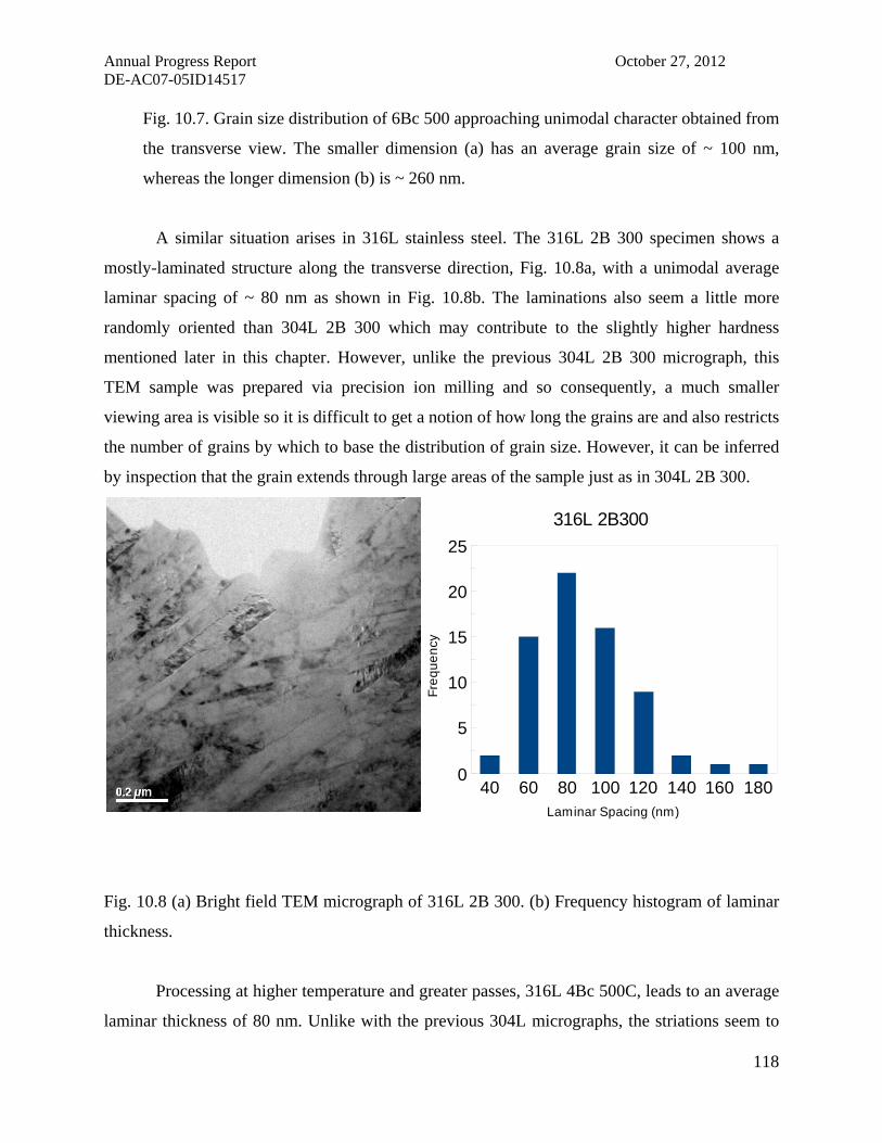
Annual Progress Report October 27, 2012 DE-AC07-05ID14517
118
Fig. 10.7. Grain size distribution of 6Bc 500 approaching unimodal character obtained from
the transverse view. The smaller dimension (a) has an average grain size of ~ 100 nm,
whereas the longer dimension (b) is ~ 260 nm.
A similar situation arises in 316L stainless steel. The 316L 2B 300 specimen shows a
mostly-laminated structure along the transverse direction, Fig. 10.8a, with a unimodal average
laminar spacing of ~ 80 nm as shown in Fig. 10.8b. The laminations also seem a little more
randomly oriented than 304L 2B 300 which may contribute to the slightly higher hardness
mentioned later in this chapter. However, unlike the previous 304L 2B 300 micrograph, this
TEM sample was prepared via precision ion milling and so consequently, a much smaller
viewing area is visible so it is difficult to get a notion of how long the grains are and also restricts
the number of grains by which to base the distribution of grain size. However, it can be inferred
by inspection that the grain extends through large areas of the sample just as in 304L 2B 300.
Fig. 10.8 (a) Bright field TEM micrograph of 316L 2B 300. (b) Frequency histogram of laminar
thickness.
Processing at higher temperature and greater passes, 316L 4Bc 500C, leads to an average
laminar thickness of 80 nm. Unlike with the previous 304L micrographs, the striations seem to
40 60 80 100 120 140 160 1800
5
10
15
20
25
316L 2B300
Laminar Spacing (nm)
Fre
qu
en
cy

Annual Progress Report October 27, 2012 DE-AC07-05ID14517
119
run randomly through the viewing area rather than aligning in a common direction, which may
also contribute to the observed hardness. The length of laminars has been dramatically reduced
compared to the 316L 2B 300C specimen. This may in fact be an evidence of a tendency to form
equiaxed grains after more ECAP extrusions. Indeed, the appearance of what may be equiaxed
grains is apparent from the TEM micrograph in fig 10.9 (a). This appearance persists throughout
the entire viewing area and so indicates a uniformity of overall microstructural refinement.
(a)
Fig. 10.9. (a) TEM micrograph of 316L 4Bc 500. (b) Frequency histogram of laminar thickness.
60 80 100 120 140 1600
5
10
15
20
25
316L 4Bc500
Transverse View
D (nm)
Fre
qu
en
cy

Annual Progress Report October 27, 2012 DE-AC07-05ID14517
120
Mechanical Properties
The hardness evolutions of 304L and 316L before and after processing are summarized in
Table 4.3. As expected, it can be seen that material hardening increases with further processing.
In both 304L and 316L, significant hardening can be seen in their respective 1A RT processing.
While this may be easily attributed primarily to the presence of martensite in 304L, it’s slightly
more difficult to account for in 316L considering the predominance of austenite with only a
slight fraction of martensite. Hardness increases steadily with further processing at higher
temperatures, however, which is consistent with the observed grain size refinement previously
discussed. The hardness of 316L seems to increase faster than that of 304L since the hardness of
316L 4Bc 500 is comparable to that of 304L 6Bc 500. This strengthening trend will also be
apparent in the results from tensile tests to be discussed later.
Table 10.3. Hardness (HIT) evolution of ECAPed samples after ECAP processing.
SS 304L SS 316L
Annealed 2.20 ± 0.05 GPa 2.10 ± 0.03 GPa
1A RT 5.70 ± 0.09 GPa 4.90 ± 0.12 GPa
2B 300 4.30 ± 0.09 GPa 4.60 ± 0.13 GPa
4Bc 500 4.80 ± 0.14 GPa 5.10 ± 0.16 GPa
6Bc 500 5.10 ± 0.17 GPa N/A
In collaboration with Dr. Maloy at Los Alamos National Laboratory, tensile tests have
been performed on three ECAPed specimens. Overall reduction in billet dimensions after
subsequent processing limited the number of tensile test samples to two. The stress-strain curves
for each processed material are presented in Fig. 10.10.
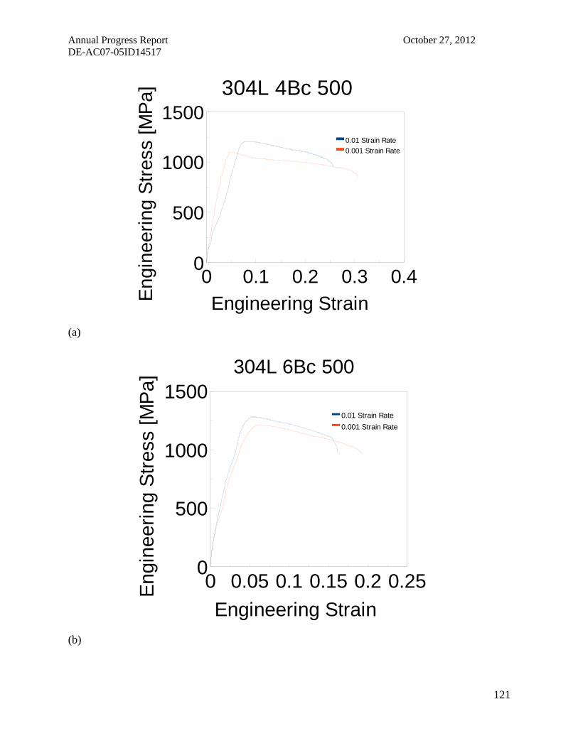
Annual Progress Report October 27, 2012 DE-AC07-05ID14517
121
(a)
(b)
0 0.1 0.2 0.3 0.40
500
1000
1500304L 4Bc 500
0.01 Strain Rate
0.001 Strain Rate
Engineering StrainEng
inee
ring
Str
ess
[MP
a]
0 0.05 0.1 0.15 0.2 0.250
500
1000
1500304L 6Bc 500
0.01 Strain Rate
0.001 Strain Rate
Engineering Strain
Eng
inee
ring
Str
ess
[MP
a]

Annual Progress Report October 27, 2012 DE-AC07-05ID14517
122
(c)
0 0.05 0.1 0.15 0.20
500
1000
1500316L 4Bc 500
0.01 Strain Rate
0.001 Strain Rate
Engineering StrainEng
inee
ring
Str
ess
[MP
a]
Fig. 10.10. Stress-Strain curves for (a) 304L 4Bc 500 (b) 304L 6Bc 500 and (c) 316L 4Bc 500. The two curves on each graph represent different strain rates.
It can be seen that there is an increase in yield stress from 304L 4Bc 500 to 304L 6Bc
500. 304L 4Bc 500 appears to be the most ductile of all the specimens considering the high
amount of strain it is able to withstand before fracture. It also appears to have a comparable yield
stress to those of 304L 6Bc 500 and 316L 4Bc 500. However, it is also important to note that
there is an evident sensitivity to strain rate in 304L 4Bc500 specimen as the yield stress increases
by about 200 MPa when the strain rate is increased by a factor of ten. This strain rate dependence
is also apparent in 304L 6Bc 500 albeit to a lesser degree. Interestingly, 316L 4Bc 500 has a
comparable yield stress and fracture strain to that of the 6-pass 304L sample indicating that
similar grain refinement is achieved in 316L, but there appears to be very limited strain rate
sensitivity in 316L SS.
The yield stress and strain at fracture for each specimen are summarized in Table 10.4.
The comparisons show that the yield strength of 304L 4Bc500 specimen is lower than the other
two specimens, but with greater strain to fracture. The yield strength and ductility of 304L
6Bc500 and 316L 4Bc 500 specimens are similar.

Annual Progress Report October 27, 2012 DE-AC07-05ID14517
123
Table 10.4. Summary of uniaxial tensile test for as-processed 304L and 316L at various strain rates.
Specimen Strain Rate [s-1] Yield Stress [GPa] Strain at Fracture
304L 4Bc 500 0.001 1.099 .31
304L 4Bc 500 0.01 1.210 .26
304L 6Bc 500 0.001 1.212 .19
304L 6Bc 500 0.01 1.285 .16
316L 4Bc 500 0.001 1.253 .16
316L 4Bc 500 0.01 1.284 .18
Analysis of fracture surfaces for all specimens, Fig. 10.11 a-c, indicates a ductile fracture
mode for all specimens tested at the same strain rate of 10-3s-1. Ductile dimples are observed in
all specimens, and they become finer in 304L specimens processed at a higher number of passes.
The dimples in 316L 4Bc 500 are comparable to those of 304L 6Bc 500 confirmed by their
comparable yield stresses and strain-at-fracture.

Annual Progress Report October 27, 2012 DE-AC07-05ID14517
124
(a)
(b)

Annual Progress Report October 27, 2012 DE-AC07-05ID14517
125
(c)
Fig. 10.11. FESEM micrographs of the fracture surfaces of (a) 304L 4Bc 500, (b) 304L 6Bc 500,
and (c) 316L 4Bc500 specimens tested at a strain rate of 10-3s-1.
Microstructure
The appeal of X-Ray diffraction is its versatility while remaining a non-destructive and
powerful technique to analyze the microstructure of materials. Our primary interest in using this
technique is to characterize the effects of ECAP on the microstructure of our stainless steels. It's
been reported in the literature that austenitic steels subjected to ECAP tend to form
predominantly martensite phases after numerous Bc processing at room temperature (ref: Bulk
nanocrystalline stainless steel fabricated by equal channel angular pressing). Huang et. al. Report
~83% volume fraction of martensite after 8 passes following this route. It appears that there is
probably a temperature dependence on this so-called deformation induced martensite
transformation (DIMT) (ref: Formation mechanism of nanostructures in austenitic stainless steel
during equal channel angular pressing ) since, our multiple passes (4 – 6) at higher temperature
did not impart such a noticable or significant quantity of martensite as can be seen from, for
example, the ECAP 4-pass specimen reported by Huang et. al. in Fig. 10.12. No information of

Annual Progress Report October 27, 2012 DE-AC07-05ID14517
126
processing temperature was made in that study by Huang et. al., however it can be inferred that it
was performed at lower temperatures than our sample based on our results for 304L.
Fig. 10.12. XRD of microstructural evolution of ECAP 304L SS as produced by Huang et. al.
Formation of Fine Austenite Grains
Microstructural refinement is achieved primarily through the action of deformation
twinning during severe plastic deformation. Plastic shear strain at the beginning of the ECAP
process produces a high density of deformation twins. These twin boundaries subdivide the
original grains in to thin plate-like grains whose thickness are in submicron regime while the
length extends through much of the original coarse grains. Successive processing via ECAP
further divides these grains due to shear deformation from different directions consequent of the
90o rotations between passes. This happens because large dislocation clusters are introduced into
the twin grains generated from the initial passes in order to accommodate further plastic strain.
These dislocations develop in to grain boundaries via the action of additional ECAP processing.

Annual Progress Report October 27, 2012 DE-AC07-05ID14517
127
ECAP also allows for the formation of fine-grained austenite grains via the mechanism of twin
fragmentation. Grain refinement mechanisms transform from that of the dislocation division
previously discussed to a so-called twin fragmentation mechanism. A limiting grain size
refinement is restricted by factors such as stacking fault energy. A high-enough stacking fault
energy tends to a fast dynamic recovery of dislocations during deformation. This prevents the
dislocations from forming in to grain boundaries. It is unclear why we would witness less
recovery of dislocations with processing at higher-than-room temperature. Twin boundaries also
act as obstacles to dislocation recovery. As mentioned earlier, results from TEM show the
formation of these platelets which gradually evolve in to equiaxed-looking grains.
Discussion - Mechanical Properties
It is well known that nanocrystalline or fine grained materials exhibit superior mechanical
properties. We see from our studies that the refined grains produce harder material with increases
in yield stress and decreased sensitivity to strain rate. It is usually suspected that finer grains
should also lead to increase in material ductility. Such was not the case in our study. We find that
there is an overall decrease in ductility from samples of lesser processing to those of more. This
is not totally unexpected since such heavy deformation due to our processing is not without
artifacts such as pores and tensile instabilities [Reference: the mechanical properties of
nanocrystalline materials], although this effect can be diminished by using tensile specimens of
such small geometry as ours. This trade of ductility for yield stress in bulk materials should thus
be expected. This may also support the notion that a high density of dislocations induced by
processing may play a role in the grain refining process. The increase in hardness is also
consistent with the notion that ECAP introduces such dislocations. While hardness is typically
reported as Vicker's hardness, we opted to report indentation hardness instead.

Annual Progress Report October 27, 2012 DE-AC07-05ID14517
128
Section B. South Korea contribution
As our South Korea counterpart mainly focused on ODS steels, here we only summary
the projects in which US side has been actively involved.
B 11. Microstructure and mechanical properties of ECAP processed ODS steels, PM 2000,
and torsion studies of 316 stainless steels.
Lead organization: KAERI (Lead by Dr. Jinsung Jiang)
11.1. ECAPed ODS steels
The microstructure of ECAPed ODS steel was also examined by TAMU as reported in
the previous section. However, the goal of TAMU experiments is to investigate He and heavy
ion irradiation induced defects. KAERI will focus on the evolution of microstructure and
mechanical properties after ECAP processes. The following summarize the contributions from
the Korean side of the team.
Fe-base oxide dispersion strengthened (ODS) alloy samples were prepared by MA
(mechanical alloying) of elemental powders of Fe with about 70 micron in diameter, Cr, Ni, Mo,
Ta, Ti of less than 10 micron, and yttria of about 20 nm in size. Two heats of the samples were of
17%Cr, 12%Ni austenitic steels; and the other two were 12%Cr ferritic-martensitic steels. MA
processes were carried out using a planetary ball mill running in the Ar-filled atmosphere
controlled glove box. Ball to powder ratio was 15:1 and the milling time was 12 hrs. For
consolidation of MA powders HIP (hot isostatic pressing) process was done at 1150oC for 4 hrs
under 100 atm pressure, following hydrogen reduction process by 5% hydrogen mixture gas to
control the oxygen content in MA powders and degassing process. Nominal compositions of
samples are shown in Table 6.1, and round rods with 12 mm in diameter and 150 mm long were
cut out from the HIP processed samples. ECAP process of ODS steel samples were carried out at
Texas A&M University
Table 11.1 Nominal composition of ODS samples for ECAP process
2101 Fe-17Cr-12Ni-2.5Mo-0.3Ti-0.3Y2O3
2102 Fe-17Cr-12Ni-2.5Mo-0.3Ti-0.3Y2O3-0.002B
2103 Fe-12Cr-1.1W-0.2V-0.14Ta-0.3Y2O3
2104 Fe-12Cr-1.1W-0.2V-0.14Ta-0.3Y2O3-0.002B

Annual Progress Report October 27, 2012 DE-AC07-05ID14517
129
Microstructural characterization
Grain boundary evolution of ECAPed ODS steel sample
For EBSD analyses all ECAPed ODS samples were mechanically polished and then
electrolytically polished in 10% perchloric acid with ethanol solution cooled with the liquid
nitrogen at 20 V for 30 sec. EBSD analyses were done with JEOL 6500F with the accelerating
voltage of 20 kV and probe current of 4 nA. The pixel step size was controlled with 0.02 micron
and carried out with Package 5 of HKL.
Band contrast of ECAPed ODS steel samples are shown in Fig. 11.1. Grain sizes of all
the ECAPed ODS samples reveal that significantly smaller than those of original ODS samples
that are in the range of 5-10 micron in diameter. Especially ODS samples with austenitic matrix
shows relatively uniform 0.5-1.0 micron in size of grains after ECAP process (Fig. 11.1 (a) and
(b) ). On the other hand the ODS samples with ferritic/martensitic matrix phase reveal grain size
distribution somewhat differently; i.e. ODS alloy sample 2103 which showed the grain size of
about 5 micron before ECAP process reveals very fine grain structure after ECAP, but the
sample 2104 with the original grain size of above 10 micron shows coarser grain structure.
Therefore the grain size distribution after ECAP process seems to dependant on the initial grain
size distribution (Fig. 11.1 (c) and (d)). Compared with ECAP 2C (rotation of 180o between
pressings) 2B samples reveals bigger aspect ratio (more elongated) of grain morphologies due to
the characteristics of 2C scheme which rotates the sample 180o between the pressings and
applies reverse shear after eformation and annihilates the directionality of the deformation.
Main texture of fcc materials which go through the simple shear deformation usually
shows {111} planes parallel to shear plane, and {110} planes to shear plane in case of bcc
materials. Shear planes and inverse pole figures of the ECAPed ODS samples are shown in Fig.
11.2 and 11.3. In 2101 and 2102 samples which have fcc structure it is explicitly shown that
{111} texture is well developed. In the sample 2104 which has bcc (ferritic/martensitic) structure
reveals well developed {110} texture, while 2103 shows not very well developed texture.

Annual Progress Report October 27, 2012 DE-AC07-05ID14517
130
(a) (b)
(c) (d)
(e) (f)
Fig. 11.1 Grain structure by EBSD band contrast map of ECAPed ODS steel samples; (a) 2101, ECAPed via 2C scheme at 800oC (b) 2102, ECAPed via 2C scheme at 800oC (c) 2103, ECAPed via 2b scheme at 800oC (d) 2101, ECAPed via 2B scheme at 800oC, (e) 2103, ECAPed via 2B scheme at 700oC, and (f) 2104, ECAPed via 2B scheme at 700oC

Annual Progress Report October 27, 2012 DE-AC07-05ID14517
131
Low angle boundary and twin boundary distributions are illustrated in Fig. 3-4 and 3-5
respectively. Low angle boundaries here are defined as the boundaries with the misfit angle
between 3 and 15o. Significant portion of the boundary contours in the band contrast maps (Fig.
3-1) appear matched with the low angle boundaries. High density of twin boundary are revealed
within 2101 and 2102 ODS samples with austenite structure, while twin boundary is very rarely
observed in 2104 sample of bcc structure with relatively large grain size.
(a) 2101 2C800 (b) 2102 2C800
(C) 2103 2C700 (d) 2104 2C700
(e) 2103 2B700 (f) 2104 2B700

Annual Progress Report October 27, 2012 DE-AC07-05ID14517
132
Fig. 11.2 Normal direction orientation map of ECAPed ODS samples
(a) 2101 2C800 (b) 2102 2C800
(c) 2103 2C700 (d) 2104 2C700
(e) 2103 2B700 (f) 2104 2B700
Fig. 11.3 Low angle grain boundary map of ECAPed ODS samples.

Annual Progress Report October 27, 2012 DE-AC07-05ID14517
133
(a) 2101 2C800 (b) 2102 2C800
(c) 2103 2C700 (d) 2104 2C700
(e) 2103 2B700 (f) 2104 2B700
Fig. 11.4 Twin boundary map pf ECAPed ODS samples
Hardness measurement

Annual Progress Report October 27, 2012 DE-AC07-05ID14517
134
Vickers hardness of ECAPed ODS samples were measured four times each and compared
with those of the samples before the process. Hardness increased significantly by ECAP
processes, except sample 2103 which showed not very big change of the grain size distribution
before and after ECAP process. Different ECAP schemes (2C vs. 2B) appear not to influence the
hardness change much. Further ECAP process with different temperature, schemes, and
especially the number of passes would be needed to understand more comprehensively the
effects of the ECAP process on the mechanical properties.
Fig. 11.5 Vickers hardness change of ECAPed ODS samples
(A: 2101; B: 2102; C: 2103; D: 2104
E : 2101 2C800; F: 2102 2C800; G: 2103 2C700; H: 2104 2C700
I: 2103 2B700; J: 2104 2B700)
11.2. In-situ microstructure analysis of PM 2000 during uniaxial deformation.
The microstructure and microtexture evolution of ODS steel during uniaxial tensile
deformation was investigated. Specimens were elongated by an in-situ uniaxial deformation
stage equipped with high-resolution electron backscattered diffraction (HR-EBSD) system.
Microstructure and orientation rotating behaviors of individual grains were traced during the
each step of the deformation process. ODS steel was found to change its crystallographic
orientation on deformation, depending on its initial orientations. Further, the relationship
between its mechanical properties and the distribution of dislocations was analyzed by

Annual Progress Report October 27, 2012 DE-AC07-05ID14517
135
transmission electron microscopy (TEM) under uniaxial deformation. This result clarifies the
knowledge of the relationship between the microstructure, mechanical properties and
deformation of ODS steel.
The nominal chemical composition of PM 2000 is Fe-20Cr-5.5Al-0.5Ti-0.5Y2O3 (in
wt.%). Fig. 11.6 shows the specially designed micro deformation device used to measure the
crystallographic orientation change by EBSD during uniaxial tension. The uniaxial tensile
sample was obtained from the edge of the extruded bar and its tensile direction was parallel to
the extrusion direction. The specimen was polished mechanically down to a thickness of 300 μm.
Electro polishing was carried out for 30 s at 20 V and a flow rate of 20 using a solution of 10 %
perchloric acid and 90 % ethanol. To measure the strain amount and trace the microstructure of
the same area during deformation, four rectangular micro indentation marks were placed on the
specimen surface of length 140 μm, as shown in Fig. 11.6 (a). Macroscopic strains at each
deformation step were obtained by measuring the relative displacement of the indentation marks
along the tensile direction in the SEM images. The tensile strain was measured to be about 17 %
along one direction. Fig. 11.6 (b) and (c) are digital images of the micro deformation device
before and after the uniaxial tensile test.
Fig. 11.6 Schematic representation and images of uniaxial deformation device for EBSD measurements (a) Sample shape for uniaxial deformation (thickness = 300mm), images of uniaxial deformation device (b) before and (c) after uniaxial deformation.
(a) (b)
(c)
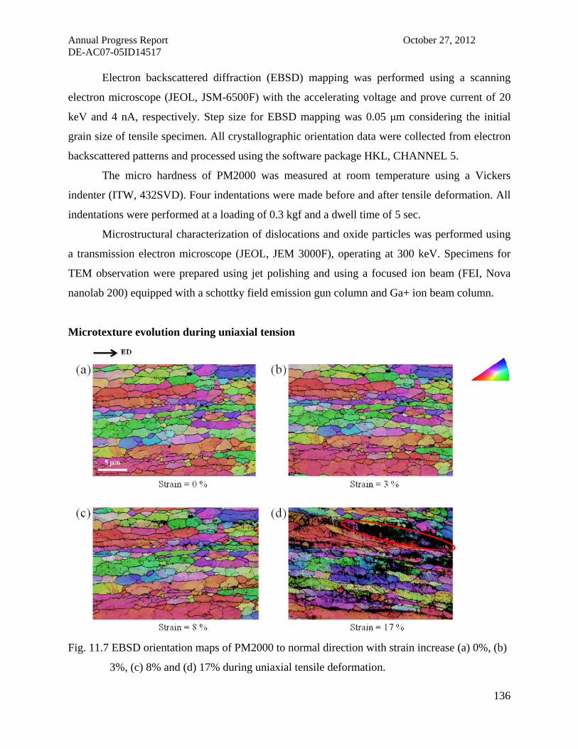
Annual Progress Report October 27, 2012 DE-AC07-05ID14517
136
Electron backscattered diffraction (EBSD) mapping was performed using a scanning
electron microscope (JEOL, JSM-6500F) with the accelerating voltage and prove current of 20
keV and 4 nA, respectively. Step size for EBSD mapping was 0.05 μm considering the initial
grain size of tensile specimen. All crystallographic orientation data were collected from electron
backscattered patterns and processed using the software package HKL, CHANNEL 5.
The micro hardness of PM2000 was measured at room temperature using a Vickers
indenter (ITW, 432SVD). Four indentations were made before and after tensile deformation. All
indentations were performed at a loading of 0.3 kgf and a dwell time of 5 sec.
Microstructural characterization of dislocations and oxide particles was performed using
a transmission electron microscope (JEOL, JEM 3000F), operating at 300 keV. Specimens for
TEM observation were prepared using jet polishing and using a focused ion beam (FEI, Nova
nanolab 200) equipped with a schottky field emission gun column and Ga+ ion beam column.
Microtexture evolution during uniaxial tension
Fig. 11.7 EBSD orientation maps of PM2000 to normal direction with strain increase (a) 0%, (b)
3%, (c) 8% and (d) 17% during uniaxial tensile deformation.

Annual Progress Report October 27, 2012 DE-AC07-05ID14517
137
Tensile deformation was discontinued at three different uniaxial strains to investigate the
various characteristics before necking. Fig. 11.7 (a) exhibits elongated grains of size 1-7 µm
along the ED. The aspect ratio of the grains increased with an increase in grain size because of
the elongation of grains along the tensile direction. The grains rotated towards the stable
orientation, and highly deformed grains increase as observed from dark contrast in the
orientation map (Fig. 11.7 (d)). The area of the green region indicates that <101>//ND decreases
as the uniaxial strain increases. The areas of the red and blue regions indicate that <001>//ND
and <111>//ND increase with the strain, respectively. It is indicated that <101>//ND rotates
towards <001>//ND or <111>//ND during uniaxial deformation.
Vickers hardness test and TEM analysis
SEM images of Vickers indentation marking indented before and after deformation are
shown in Fig. 11.8 (a). Four indentation marks are clearly seen on both images, highlighted with
blue and red circles. The average diagonal distance of each specimen before and after
deformation is 39.7μm and 43.5μm, respectively. Fig. 11.8 (b) shows the relation between the
average Vickers hardness and the indented area. The graph indicates that 17 % of the hardness
increases during uniaxial deformation. That is, the increase in hardness is related to the
hardening mechanism by deformation known as work hardening.

Annual Progress Report October 27, 2012 DE-AC07-05ID14517
138
Fig. 11.8 (a) SEM images of micro Vickers indentation marking at as extruded area and
deformed area, (b) average Vickers hardness related to indentation areas.
The TEM sample was prepared by jet polishing before deformation and its high
resolution microstructure images are shown in Fig. 11.9. Dark field images were taken the
scanning transmission electron microscopy (STEM) mode to obtain clear contrast images of
oxide particles and dislocations. Oxide particles of 10-20 nm were uniformly dispersed inside the
grains. A few particles over 100 nm were also observed. A number of dislocations are pinned by
oxide particles because the sample is hot extruded without any heat post-treatment.
(a) (b)
Fig. 11.9. STEM dark field images of as extruded area.
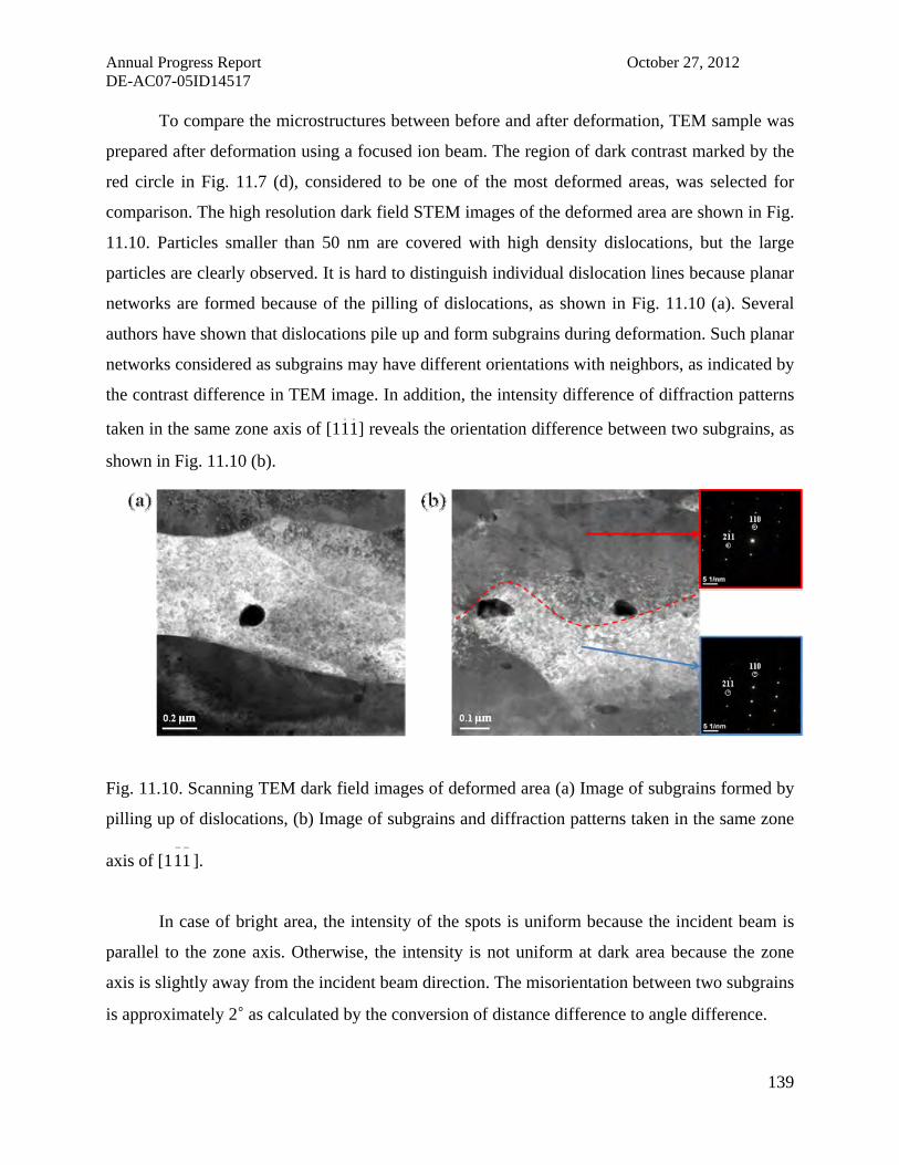
Annual Progress Report October 27, 2012 DE-AC07-05ID14517
139
To compare the microstructures between before and after deformation, TEM sample was
prepared after deformation using a focused ion beam. The region of dark contrast marked by the
red circle in Fig. 11.7 (d), considered to be one of the most deformed areas, was selected for
comparison. The high resolution dark field STEM images of the deformed area are shown in Fig.
11.10. Particles smaller than 50 nm are covered with high density dislocations, but the large
particles are clearly observed. It is hard to distinguish individual dislocation lines because planar
networks are formed because of the pilling of dislocations, as shown in Fig. 11.10 (a). Several
authors have shown that dislocations pile up and form subgrains during deformation. Such planar
networks considered as subgrains may have different orientations with neighbors, as indicated by
the contrast difference in TEM image. In addition, the intensity difference of diffraction patterns
taken in the same zone axis of [11-
1-
] reveals the orientation difference between two subgrains, as
shown in Fig. 11.10 (b).
Fig. 11.10. Scanning TEM dark field images of deformed area (a) Image of subgrains formed by
pilling up of dislocations, (b) Image of subgrains and diffraction patterns taken in the same zone
axis of [111
].
In case of bright area, the intensity of the spots is uniform because the incident beam is
parallel to the zone axis. Otherwise, the intensity is not uniform at dark area because the zone
axis is slightly away from the incident beam direction. The misorientation between two subgrains
is approximately 2° as calculated by the conversion of distance difference to angle difference.

Annual Progress Report October 27, 2012 DE-AC07-05ID14517
140
The effect of oxide particles and dislocations on microstructures and their mechanical
properties was investigated by Vickers hardness test and TEM analysis. A 17 % increase in
hardness was found after deformation because the microstructure development was related to the
dislocations and oxide particles. This study suggested that the finely dispersed oxide particles
might contribute to form a cell structure of dislocation entanglement which increases not only the
hardness of the material but also the orientation spreads in the microstructure.
11.3. Shear and inverse shear deformation by torsion of 316L stainless steel
During torsion the sample material experiences simple shear deformation without volume
change. The extent of the deformation could be easily and quantitatively controlled during
torsion test and the microstructural change could be observed with the deformation. Shear strain
during torsion is defined by = tan (), and texture is usually developed by the same amount of
tensile and compression force which are perpendicularly working each other. Two deformation
modes are possible; the inverse shear deformation is that the sample is deformed in the other
(reverse) direction with the same amount after one simple torsion (shear) deformation. In this
case total shear becomes macroscopically zero, but the deformed structure is not completely
reversible and the remained deformation becomes more distinctive as the extent of shear
becomes bigger.
Torsion specimen was prepared with SUS 316L. Test section was 5 mm in diameter; 10
mm in length and the grip portion was 30 mm square bar with the total sample length of 70 mm.
After the torsion test the sample surface (perpendicular to the cylinder sample radius) was
observed using TEM/EBSD (ASTAR).
Torsion samples before and after the test are shown in Fig. 11.11. The increasing amount
of shear deformation from 0 to 0.4, 0.8, and up to 1.6 is clearly revealed in Fig. 11.11 (c).
(a)
(b)

Annual Progress Report October 27, 2012 DE-AC07-05ID14517
141
(c)
Fig. 11.11. Torsion test samples of 316L stainless steel; before and after the tests with the marks.
(a) (b) (c)
(d) (e) (f)
Fig. 11.12 TEM and EBSD analyses of torsion tested 316L stainless steel sample;
(a) TEM BFmicrograph, (b) Phase map (blue: austenite, red: martensite), (c)
Reliability, (d) Normal direction orientation map, (e) sub-grain boundary map (3 o
< misorientation < 15o), and (f) twin boundary (3) map

Annual Progress Report October 27, 2012 DE-AC07-05ID14517
142
B12. Microstructural Evolution of ECAPed Fe–17Cr-12Ni-2.5Mo austenitic alloys with Fe+
and H+ ion irradiation
Lead organization: KAERI (Lead by Dr. Jinsung Jiang)
In this study, microstructure evolutions of the Fe-17Cr-12Ni-2.5Mo and ODS alloys during
Fe+ and H+ ion irradiations were investigated. Radiation-induced defect distributions have been
examined; it was observed that the interstitials traveled further than substitutions and interacted
with grain boundaries preferentially. Moreover, it was observed that crystal structure of
irradiated sample surface was changed from FCC to BCC while the Fe-17Cr-12Ni-2.5Mo alloys
were irradiated with Fe+ ion. The sizes of the newly developed BCC grains were coincident with
the ion irradiation depth, which could be estimated by simulation (SRIM 2012 software).
Chemical compositions of Fe-17Cr-12Ni-2.5Mo alloys are shown in table 12.1. Additional
2 wt% Mn and 1 w% Si were included in sample A, it was the contents of commercial 316
stainless steel. Excluding the Mn and Si contents, additional Ti and Y2O3 were added in sample
B, it was the contents of 316-type ODS stainless steel. The ODS sample was fabricated by
mechanical alloying and hot isostatic pressing processes. Elemental metal powders with yttria
powder of 30nm in size were mechanically alloyed by using a Pulverisette-5 planetary ball mill
at 200 rpm in an Ar atmosphere for 12h with a ball to powder ratio of 15:1. The MA powder was
then filled into a 304 stainless steel can, followed by degassing at 500ºC under 10-3 Pa for 1h and
sealing. The MA powder was consolidated at 1150ºC under 100MPa for 4h. The hipped bar was
then pre-heated at 1200ºC for 2h and hot rolled into a 15 mm thick plate, which corresponds to a
reduction ratio of 50%. Normalizing was performed at 1050ºC for 1h and tempering was carried
out at 750ºC for 2h. The sample was then isothermally annealed at 1250ºC for 500 h under
vacuum.
Table 12.1 Chemical composition of Fe-17Cr-12Ni-2.5Mo alloy specimens
Fe Cr Ni Mo Mn Si Ti Y2O3
A Bal 17 12 2.5 2 1 - -
B Bal. 17 12 2.5 - - 0.3 0.3
2.54 × 2.54 × 15.24 cm sized square bar of Fe-17Cr-12Ni-2.5Mo alloys were processed by
ECAP. Two different process steps are applied; the first one is a conventional ECAP process of
one pass at 25ºC (route A), the other one is a ECAP process of two passes at 800ºC, which

Annual Progress Report October 27, 2012 DE-AC07-05ID14517
143
include one more ECAP step after 180º rotation of route A processed sample (route B). After the
ECAP, samples were implanted with Fe+ and H+ ions at room temperature. The energy of Fe+ ion
source was 100keV, 2.0×1017cm-2, and the energy of H+ ion source was 120 keV, 2.0×1018cm-2,
respectively. The microstructure evolutions were investigated by TEM to examine the density of
voids, dislocations, and radiation induced segregation. The crystal structure and misorientations
in microstructures have been characterized using ASTAR, which enables orientation and phase
mapping with TEM.
In Figure 12.1, TEM micrograph of sample A and B were shown after ECAP process.
Sample A was ECAPed along the route ‘A’ at 25ºC, and Sample B was ECAPed along the route
‘C’ at 800ºC, respectively. The specimen was homogeneously deformed in figure 1(a); lots of
defects are generated in the sample, fine planar boundaries were aligned along the shear band
direction with a width of 50nm. On the other hands, an equi-axed fine grains are observed in
figure 1(b), they are induced by recrystallization with an average grain size of 500nm after
ECAP at 800°C. Those two different samples were subjected to ion irradiation tests.
Figure 12.1. TEM micrograph of sample A and B after ECAP process. (a) Sample A was
ECAPed along the route ‘A’ at 25ºC. (b) Sample B was ECAPed along the route ‘C’ at 800ºC
In figure 12.2, ion irradiation facility of KAERI is introduced. The management and
operation of the machine in figure 2(a) is currently supported by Proton Engineering Frontier
Project. Metal ions such as Ni, Cu, Co, Cr, Fe, etc. can be accelerated up to 100 keV, and the gas
ions such as He, Kr, Xe, Ar, Ne, H, etc. can be accelerated up to 120 keV. Proton Engineering

Annual Progress Report October 27, 2012 DE-AC07-05ID14517
144
Frontier Project recently tries to enlarge the acceleration voltage more than 100MeV. In figure
2(b), the irradiation samples are shown. The backing plate was made of copper, which is efficient
for thermal conduction. Samples were attached to the backing plate within the area of 5 cm X 5
cm square. Fe+ ions were irradiated at 100keV, and the dose was 2.0×10¹⁷ions/cm2. H+ ions were
irradiated at 120keV, and the dose was 2.0×10¹⁸ions/cm2.
Figure 12.2 (a) Ion irradiation facility at Gyeongju site, KAERI (b) ion irradiation test samples.
The facility is currently maintained and operated by Proton Engineering Frontier Project.
In figure 12.3, the penetration depths of ions on the Iron surface were estimated using a
molecular dynamics simulation (The software named SRIM2012). It was also assumed that Fe+
ions were irradiated at 100keV, 2.0×1017cm-2, and H+ ions were irradiated at 120keV,
2.0×1018cm-2. The results showed that the peak of Fe+ ions profile in sample would be at 30nm,
and the peak of H+ ions profile in sample would be at 500nm, respectively.
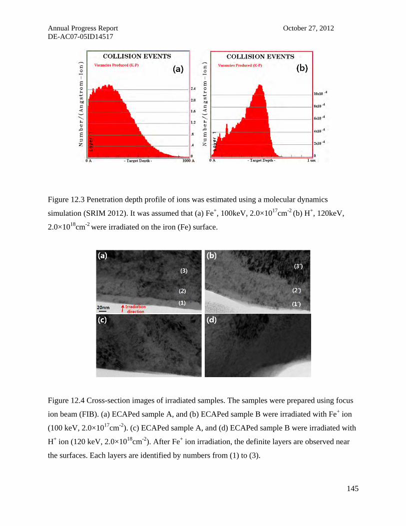
Annual Progress Report October 27, 2012 DE-AC07-05ID14517
145
Figure 12.3 Penetration depth profile of ions was estimated using a molecular dynamics
simulation (SRIM 2012). It was assumed that (a) Fe+, 100keV, 2.0×1017cm-2 (b) H+, 120keV,
2.0×1018cm-2 were irradiated on the iron (Fe) surface.
Figure 12.4 Cross-section images of irradiated samples. The samples were prepared using focus
ion beam (FIB). (a) ECAPed sample A, and (b) ECAPed sample B were irradiated with Fe+ ion
(100 keV, 2.0×1017cm-2). (c) ECAPed sample A, and (d) ECAPed sample B were irradiated with
H+ ion (120 keV, 2.0×1018cm-2). After Fe+ ion irradiation, the definite layers are observed near
the surfaces. Each layers are identified by numbers from (1) to (3).

Annual Progress Report October 27, 2012 DE-AC07-05ID14517
146
Figure 12.4 Cross-section images of irradiated samples are observed. The samples were
prepared using focus ion beam (FIB). ECAPed sample A, and sample B were irradiated with Fe+
ion source (100keV, 2.0×1017cm-2), and H+ ion source (120 keV, 2.0×1018cm-2). The damage
layers were shown near the surfaces. Specially, the definite layers are observed after Fe+ ion
irradiation. In figure 4(a), each layer was identified by numbers from (1) to (3). It was suspected
that the layer (1) and (2) are developed after irradiation, (3) is the base material. The depth was
estimated 50nm, it was coincident with the molecular dynamics simulation results. The boundary
between (1) and (2) was located in the 20nm depth, it can be the peak of ion irradiation profile.
In figure 4(b), The similar layers were observed, however, the depth of (1’) and (2’) seemed
deeper than figure 1(a). It was suspected that the grain boundaries distributions before irradiation
affected damage layer construction. In figure 4(c) and 4(d) shows H+ ion irradiation effect on the
same samples, such kind of definite layers were not observed. The H+ ions are the interstitial, the
behavior would be quite different from the substitutions, Fe+ ions.
Figure 12.5 Cross-section images of ECAPed sample A after irradiation with Fe+ ion (100 keV,
2.0×1017cm-2). Three layers which were identified in figure 4 were particularly observed from (1)
to (3), and corresponding diffraction patterns were obtained.

Annual Progress Report October 27, 2012 DE-AC07-05ID14517
147
In figure 12.5, cross-section images of ECAPed sample A after irradiated with Fe+ ion
(100keV, 2.0×1017cm-2) are suggested by magnified images. Three layers were particularly
observed from (1) to (3), and corresponding diffraction patterns were obtained. It was observed
that the crystal structure of damaged layer (1) was quite different from base material (3). Lattice
parameters could not be match as a same crystal structure. It was suspected that some major
changes were involved, such as recrystallization or phase transformation.
In figure 12.6, cross-section images of ECAPed sample B after irradiated with H+ ion (120
keV, 2.0×1018cm-2). The definite layers were observed near the surfaces. In figure 12.6(a), nano-
sized pores are finely distributted at the surface, and in figure 12.6(b), pores were gathered at the
defects such as dislocations or grain boundaries. However, there were no crystallographic change
even in the surface area, all irradiated part of samples seemed to be in one grain.
Figure 12.6 Cross-section images of ECAPed sample B after irradiation with H+ ion (120 keV,
2.0×1018cm-2). The definite layers were observed near the surfaces. (a) Nano-sized pores are
finely distributted near the surface. (b) cavities appeared to gather at the defects such as
dislocations or grain boundaries.

Annual Progress Report October 27, 2012 DE-AC07-05ID14517
148
In figure 12.7, schematic of ASTAR system is shown, basic operation concept is
introduced. ASTAR is the system which enables orientation and phase mapping with
transmission electron microscopes. It can be simply described that the TEM was accompanied by
automated diffraction pattern analysis system. The ASTAR system is effective for visualizing
crystallographic information of a sample, while it simultaneously shows the TEM micrograph.
In figure 12.8, microstructure evolutions of 17Cr-12Ni-2.5Mo alloy after Fe+ and H+ ion
irradiation was characterized using ASTAR. A virtual bright field image and a corresponding
misorientation distribution map of ECAPed sample A after irradiated with Fe+ ion irradiation
(100keV, 2.0×1017cm-2) are shown in figure 9(a) and 9(b), respectively. The same images of
ECAPed sample B after irradiated with H+ ion (120 keV, 2.0×1018cm-2) are shown in figure
12.9(c) and 9(d), respectively.
Figure 12.7 ASTAR: An orientation and phase mapping system equipped with TEM.

Annual Progress Report October 27, 2012 DE-AC07-05ID14517
149
In figure 12.9, phase and grain orientations of 17Cr-12Ni-2.5Mo alloy after Fe+ ion
irradiation (100keV, 2.0×1017cm-2) were characterized using ASTAR. In figure 9(a), reliability
factor map is shown. The reliability represents the accuracy of matching diffraction pattern data
between the calculated one and experimentally obtained one. While the reliability map is white,
the mismatch between them is small. Corresponding phase map, and grain map are shown in
figure 12.9(b) and (c), respectively. It was observed that the ion beam damaged layers at the
surface of sample A had BCC crystal structure. It means that the crystal structure of irradiated
sample surface was changed from FCC to BCC while the Fe-17Cr-12Ni-2.5Mo alloys were
irradiated with Fe+ ion. The reliability map in figure 12.9(a) supports this observation, the pattern
mismatch was suspected to be small because the color was white in the corresponding region of
reliability map.
Figure 12.8 Microstructure characterization using ASTAR (a) a virtual BF image, and (b) a
misorientation distribution map of ECAPed sample A after irradiation with Fe+ ion (100 keV,
2.0×1017cm-2) (c) a virtual BF image, and (d) a misorientation distribution map of ECAPed
sample B after irradiation with H+ ion (120 keV, 2.0×1018cm-2).

Annual Progress Report October 27, 2012 DE-AC07-05ID14517
150
Figure 12.9. Microstructure characterization by using ASTAR (a) reliability factor map, (b)
phase map, and (c) grain map of sample A after irradiation with Fe+ ion (100 keV; 2.0×1017cm-
2).
In this study, Fe-17Cr-12Ni-2.5Mo alloys were fabricated and processed by ECAP. Those
ECAPed samples were implanted with Fe+ and H+ ions at room temperature. The energy of Fe+
ion source was 100keV, 2.0×1017cm-2, and the energy of H+ ion source was 120 keV,
2.0×1018cm-2, respectively. The microstructure evolutions were investigated by TEM to examine
the density of voids, dislocations, and radiation induced segregation. The crystal structure and
misorientations in microstructures have been characterized using ASTAR, which enables
orientation and phase mapping with TEM. It was observed that the crystal structure of irradiated
sample surface was changed from FCC to BCC while the Fe-17Cr-12Ni-2.5Mo alloys were
irradiated with Fe+ ion. The sizes of the newly developed BCC grains were coincident with the
ion irradiation depth, which could be estimated by molecular dynamics simulation.
Project Milestone/Deliverable Summary:
Include a milestone/deliverable summary per template below.
Activities Milestone/Deliverable
Description
Planned
Completion
Year
Completion
Year
Preparation of Fe-Cr-Ni model
alloy and MA powder sample
Fe-Cr-Ni model alloy
sample 2009 2009

Annual Progress Report October 27, 2012 DE-AC07-05ID14517
151
(1 x 1 x 6 in)
MA powders of Fe-Cr-Ni
ECAP of austenitic steel
specimens
Nanocrystalline austenitic
alloy sample 2009 2009
ECAP of ODS alloy specimen or
Powder Consolidation of MA
powders
Nanocrystalline ODS alloy
sample 2010 2010
Interface/Grain boundary
modification by TMT
Optimum TMT conditions 2010 2010
Analyses of Interface/Grain
boundary Character & Stability
Interface/Grain boundary
engineered samples
(distinct increase of low
CSL boundary fraction)
2010 2010
Investigation of mechanical
behavior (Hardness, H/T tensile,
toughness)
Mechanical data of nano-
grain, grain boundary
engineered, and irradiated
samples
2010 2010
Ion irradiation of proton & He
ions
Irradiated samples 2011 2011
Characterization of ion irradiated
samples (irradiation cavity size
distribution, irradiation
hardening)
Irradiated samples & their
characters (morphology &
size distribution of
irradiation cavities by HR-
TEM & SANS)
2012 2012
Conference presentations/Journal
publications
Report to DOE/US & NRF/ROK
4-5
presentation/publication
per year
as requested
2012 2012
List of Publications
Presentations:

Annual Progress Report October 27, 2012 DE-AC07-05ID14517
152
1. X. Zhang, L. Shao, H. Wang and E.G. Fu, “Dose dependent radiation tolerance in Cu/V X.
Zhang, L. Shao, H. Wang and E.G. Fu, “Dose dependent radiation tolerance in Cu/V
multilayers”, MRS fall meeting, 2009, Boston, MA (oral presentation).
2. X. Zhang, Y. Yang, C. Sun, J. Gonzalez, T. Allen, and K.T. Hartwig, “Radiation damage in
nanostructured metallic materials”, Advanced Materials Working Group Meeting, University
of California, Santa Barbara, March 2010, organized by Dr. Stuart Maloy and DOE program
managers.
3. X. Zhang, “Radiation tolerant metallic multilayers and bulk ultra-fine grained steels”,
Engineering Conference International, “Innovative Materials Immune to Radiation”, Vail,
CO, Aug. 2010.
4. X. Zhang, C. Sun, Y. Yang, T. Allen, and K.T. Hartwig, “Mechanical properties and
radiation tolerance of ultra-fine grained FeCrNi alloy”, MRS fall meeting, Boston, MA, Nov.
30-Dec. 2, 2010.
5. C. Sun, J. Gonzalez, Y. Yang, T.R. Allen, S. A. Maloy, K.T. Hartwig, and X. Zhang,
E.G. Fu, “Deformation mechanisms of ultra-fine grained Fe-Cr-Ni alloys”, TMS
annual, 2011.
6. Yong Yang, Cheng Sun, Xinghang Zhang and Todd Allen, “Effect of Grain Size and
Grain Boundaries on the Proton Irradiation Response of Nanostructured Austenitic
Model Alloy”, TMS annual 2011, San Diego, CA.
7. Xinghang Zhang, L. Shao, H. Wang, E.G. Fu, Nan Li, A. Misra, Y-Q Wang, “Radiation
Tolerant Metallic Multilayers”, TMS annual 2012, Orlando, FL.
8. C. Sun, J. Ma, K.Y. Yu, K. T Hartwig, L. Shao, S.A. Maloy , X Zhang, “Mechanical
Properties and Radiation Response of Ultrafine Grained Fe-Cr-Ni Alloy”, TMS annual 2012,
Orlando, FL.
9. Yong Yang, Cheng Sun, Xinghang Zhang, Todd Allen, Irradiation Response of
Nanostructured Austenitic Model Alloy, TMS annual 2012, Orlando, FL.
10. Suk Hoon Kang, Hyung-Ha Jin, Jinsung Jang, Do Hyun Kim, Kyu Hwan Oh, Xinghang
Zhang, David C. Foley, and Karl Hartwig, “Microstructural evolution of 316L stainless steel
during ECAP process” TMS 2011 Annual Meeting, San Diego, CA, USA, Mar 2011

Annual Progress Report October 27, 2012 DE-AC07-05ID14517
153
11. Suk Hoon Kang, Jinsung Jang, Hyung-Ha Jin, Kyu Hwan Oh, “Microstructure evolution and
EBSD Band Contrast” International Union of Microbeam Analysis Society–V, Seoul, Korea,
May 2011
12. Kyu Hwan Oh, Heung Nam Han, Jun Hyun Han, Suk Hoon Kang, Do Hyun Kim, Se Jong
Kim, Yong Seok Choi “In-situ Observation of Multi-axial Deformation Behavior of Steels
using EBSD” International Union of Microbeam Analysis Society–V , Seoul, Korea, May
2011
13. D.H. KIM, EBSD measurement of deformation behavior and orientation change in dual
phase steel sheet during equi-biaxial tension, TMS 2011. (Poster)
14. Y.S. CHOI, In-situ microstructure evolution of oxide dispersion strengthened ferritic steel
under uniaxial deformation, DIANA I 2011. (Poster), Apr. 2011, Aussois, France
15. K.H. OH, In-situ Observation of Multi-axial Deformation Behavior of Steels using EBSD
Technique, IUMAS 2011. (Invited)
16. Y.S. CHOI, In-situ microstructure evolution of pure aluminum under plane strain tension,
TMS 2012. (Oral)
17. J.H. HAN, In-situ observation of dynamic recrystallization in aluminum at room temperature,
ReX GG 2013. (Oral, Abstract accepted)
Invited talks
18. “Microstructure and deformation mechanisms of ECAP processed FeCrNi alloys”, Thermec
2011, Quebec, Canada, 2011.
19. “Radiation tolerant metallic multilayers and bulk ultra-fine grained steels”, The 5th Annual
Asia-Pacific Nuclear Energy Forum on Materials for Nuclear Applications, June 2011,
Berkeley, CA.
Publications:
1. X. Zhang, E.G. Fug, A. Misra, M. J. Demkowicz, and R. G. Hoagland, “Interfaceenabled
defect reduction in He ion irradiated metallic multilayers”, JOM, Volume 62, Number 12,
75-78, DOI: 10.1007/s11837-010-0185-5, 2010 (review article).
Annual Progress Report October 27, 2012 DE-AC07-05ID14517
154
2. C. Sun, K. Y. Yu, J. H. Lee, Y. Liu, H.Wang, L. Shao, S. A. Maloy, K.T. Hartwig, and X.
Zhang, “Enhanced radiation tolerance of ultrafine grained Fe-Cr-Ni alloy”, J. Nuclear
Materials, 420 (2012) 235.
3. X. Zhang, “Radiation damage in nanostructured multilayers” (invited review article) J.
Engineering Science and Technology, under review.
4. K. Y. Yu, Y. Liu, C. Sun, E. Fu, H. Wang, L. Shao, X. Zhang, Radiation damage in
helium ion irradiated nanocrystalline Fe, Journal of Nuclear Materials, 425 (2012):140-
146.
5. C. Sun, Y. Yang, Y. Liu, K.T. Hartwig, H. Wang, S. A. Maloy, T.R. Allen, X. Zhang ,
Thermal stability of ultrafine grained Fe-Cr-Ni alloy, Materials Science and
Engineering, A, 542 (2012):64-70.
6. Hoon-Hwe Cho, Suk Hoon Kang, Sung-Hwan Kim, Kyu Hwan Oh, Heung Ju Kim,
Woong-Seong Chang, Heung Nam Han, “Microstructural evolution in friction stir
welding of high-strength line pipe steel”, Materials and Design, Volume 34, February
2012, 258–267
7. Y.S. Choi, D.H. Kim, S.-H. Kim, S.H. Kang, J. Jang, H.N. Han, and K.H. Oh, “In situ
microstructure evolution of oxide dispersion strengthened ferritic steel under uniaxial
deformation”, Journal of Nuclear Materials 428 (2012) 98–102
8. Suk Hun Kang, Hyung Ha Jin, Jinsung Jang, Yong Seok Choi, and Kyu Hwan Oh, “A
quantitative approach of microstructure evolutions by EBSD pattern quality variations”,
Microscopy and Microanalysis, submitted
9. C. Sun, M. Song, K. Y. Yu, Y. Chen, M. A. Kirk, M. Li, H. Wang, X. Zhang, In situ
evidence of defect cluster absorption by grain boundaries in irradiated nanocrystalline Ni,
Metallurgical and Materials Transactions A, submitted.
10. M. Song, C. Sun, J. Jang, C. H. Han, T. K. Kim, K. T. Hartwig, and X. Zhang,
Microstructure Refinement of a 12Cr ODS Steel by Equal Channel Angular Extrusion,
submitted.
Manuscript in preparation: N/A
11. C. Sun, S. A. Maloy, K.T. Hartwig, Y. Yang, T.R. Allen, and X. Zhang, “Deformation
mechanisms of ECAP processed Fe-Cr-Ni alloys”, in preparation.

Annual Progress Report October 27, 2012 DE-AC07-05ID14517
155
12. C. Sun, M. Kirk, M. Li, K. T. Hartwig and X.Zhang,”in situ radiation of nanocrystalline
304 stainless steel”, in preparation.
13. C. Sun, S. A. Maloy, K. T. Hartwig, L. Shao, and X. Zhang, “Heavy ion irradiation of
304 stainless steel at elevated temperature to a dose of 300dpa”, in preparation.
14. Y. Yang, T.R. Allen, C. Sun, S.A. Maloy, K.T. Hartwig, and X. Zhang, “Grain boundary
engineering of ECAPed Fe-Cr-Ni alloys”, in preparation.
15. Y. Yang, T.R. Allen, C. Sun, S.A. Maloy, K.T. Hartwig, and X. Zhang, “In situ radiation
studies of ultra fine grained Fe-Cr-Ni alloys”, in preparation.
Summary and Benefit statement
This is a very successful project that falls right under the current theme of NanoNuclear.
Significant amount of work has been performed to refine the microstructure of austenitic
stainless steels. Studies show that these nanograined steels have extraordinary radiation tolerance
against He, Kr and Fe ion irradiation compared with their coarse grained counterparts.
Meanwhile the nanograined steels have high strength and maintained reasonable ductility.
Nanocrystalline 304 and 316L stainless steels are thermally stable up to 600oC. The next step
(phase 2) of the project shall be 1) investigation of the neutron radiation tolerance of these
nanograined steels; and 2) radiation resistance up to 300 dpa.
Furthermore our collaborations with South Korea collaborators through INERI have been
very fruitful. We have proved that ECAP is efficient to change the chemistry and refine the size
and distribution of oxide nanoparticles. ECAP is thus a promising technique for thermo-
mechanical treatment of a variety of steels and alloys.
More than a dozen research articles have been (or will be) published as a result of this
project. Numerous talks (including invited talks) have been delivered at national and
international conference. 5 Graduate students have been supported by this project.
We are grateful for collaborations with Dr. Stuart Maloy at Los Alamos National
Laboratory on mechanical testing and Dr. Don Brown on neutron scattering studies. We
acknowledge the access to Argonne-IVEM in situ radiation facility and collaboration with Drs.
Mark Kirk and Meimei Li at Argonne National Laboratory.