
Bulk MEMS 2013, Part 2 [email protected]. Micro hot plate: how many litho steps ? Pt heater...
34
Bulk MEMS 2013, Part 2 sami.franssila@aalt o.fi
-
Upload
ross-norton -
Category
Documents
-
view
223 -
download
2
Transcript of Bulk MEMS 2013, Part 2 [email protected]. Micro hot plate: how many litho steps ? Pt heater...
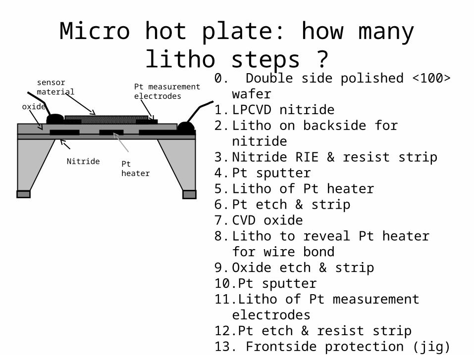
Micro hot plate: how many litho steps ?
Pt heaterNitride
Pt measurement electrodes
sensor material
oxide
0. Double side polished <100> wafer1. LPCVD nitride2. Litho on backside for nitride3. Nitride RIE & resist strip4. Pt sputter5. Litho of Pt heater6. Pt etch & strip7. CVD oxide8. Litho to reveal Pt heater for wire bond9. Oxide etch & strip10.Pt sputter11.Litho of Pt measurement electrodes12.Pt etch & resist strip13. Frontside protection (jig)14.Backside KOH etch15.Sensor material depo & patterning
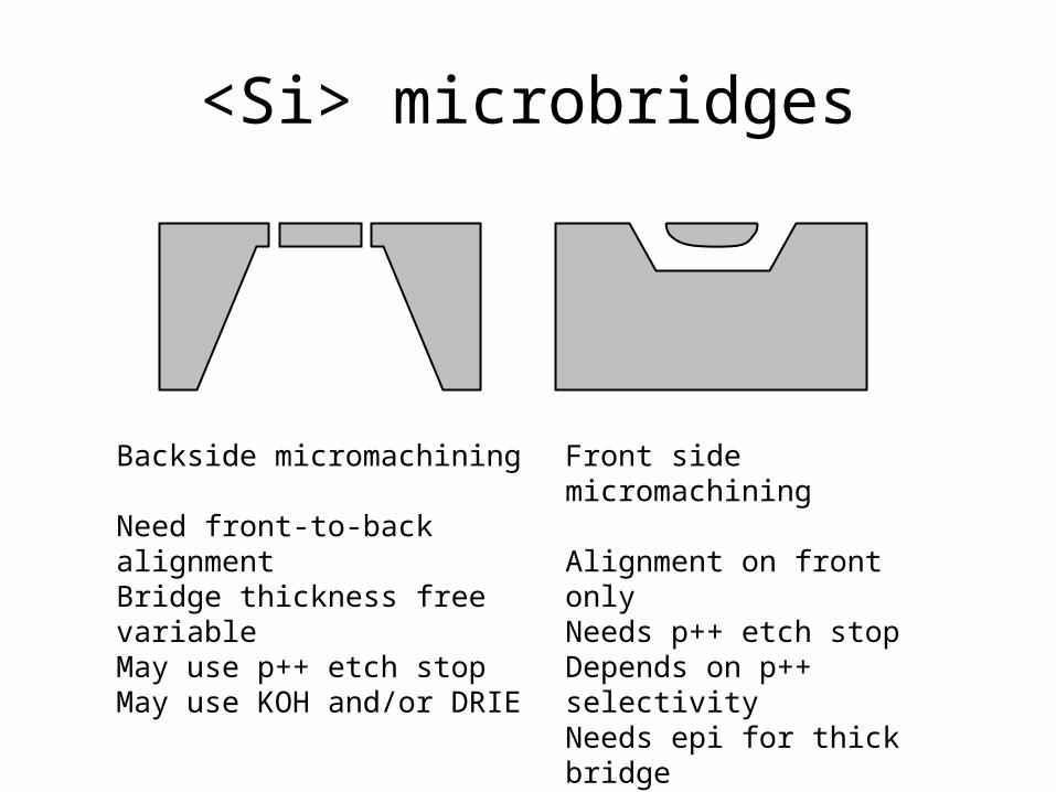
<Si> microbridges
Backside micromachining
Need front-to-back alignmentBridge thickness free variableMay use p++ etch stopMay use KOH and/or DRIE
Front side micromachining
Alignment on front onlyNeeds p++ etch stopDepends on p++ selectivityNeeds epi for thick bridgeWider bridge depth under larger

Double side alignment
Double sided lithography requires DSP wafers
(Double Side Polished)
Some alignments are critical but not all !
Often the backside structures are large, and not critically aligned to top side features.

Alignment: diffused piezoresistors
Piezoresistors have to be positioned at the maximum defelection region
OK NOT OK
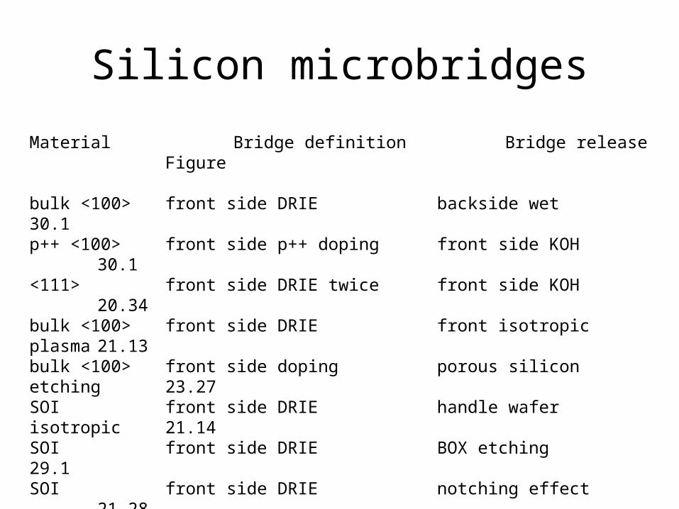
Silicon microbridges
Material Bridge definition Bridge release Figure bulk <100> front side DRIE backside wet 30.1p++ <100> front side p++ doping front side KOH 30.1<111> front side DRIE twice front side KOH 20.34bulk <100> front side DRIE front isotropic plasma 21.13bulk <100> front side doping porous silicon etching 23.27SOI front side DRIE handle wafer isotropic 21.14SOI front side DRIE BOX etching 29.1SOI front side DRIE notching effect 21.28cavity SOI front side DRIE none required 30.18
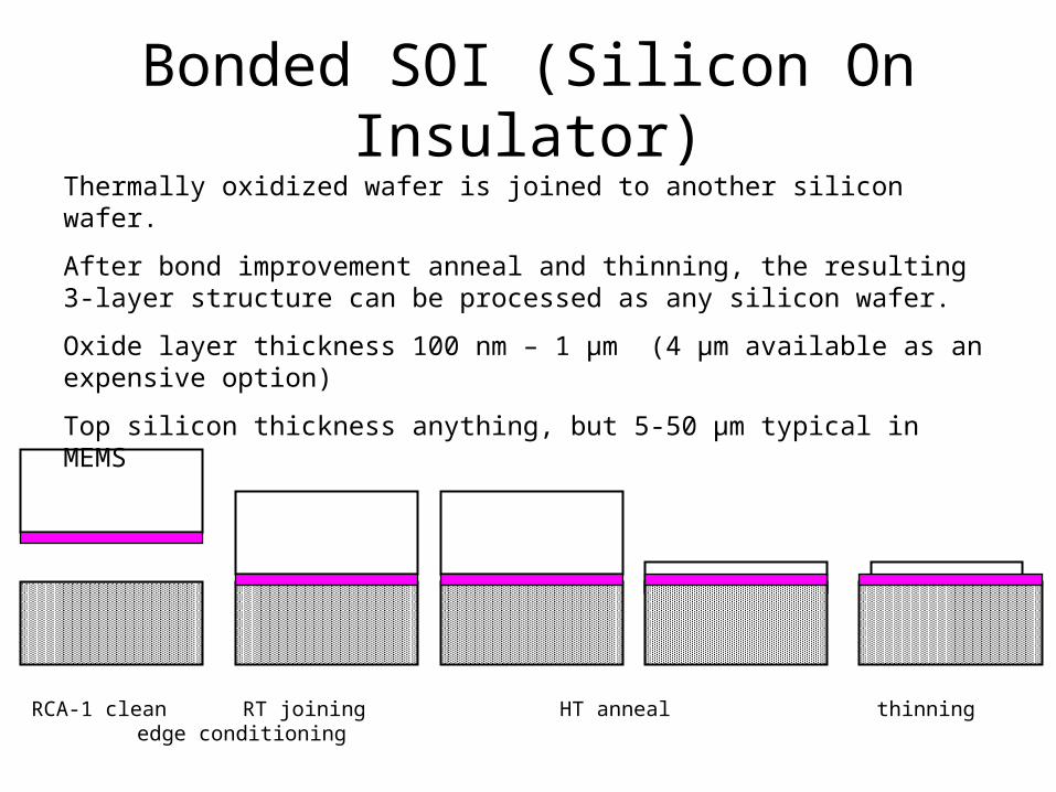
Bonded SOI (Silicon On Insulator)
RCA-1 clean RT joining HT anneal thinning edge conditioning
Thermally oxidized wafer is joined to another silicon wafer.
After bond improvement anneal and thinning, the resulting 3-layer structure can be processed as any silicon wafer.
Oxide layer thickness 100 nm – 1 µm (4 µm available as an expensive option)
Top silicon thickness anything, but 5-50 µm typical in MEMS
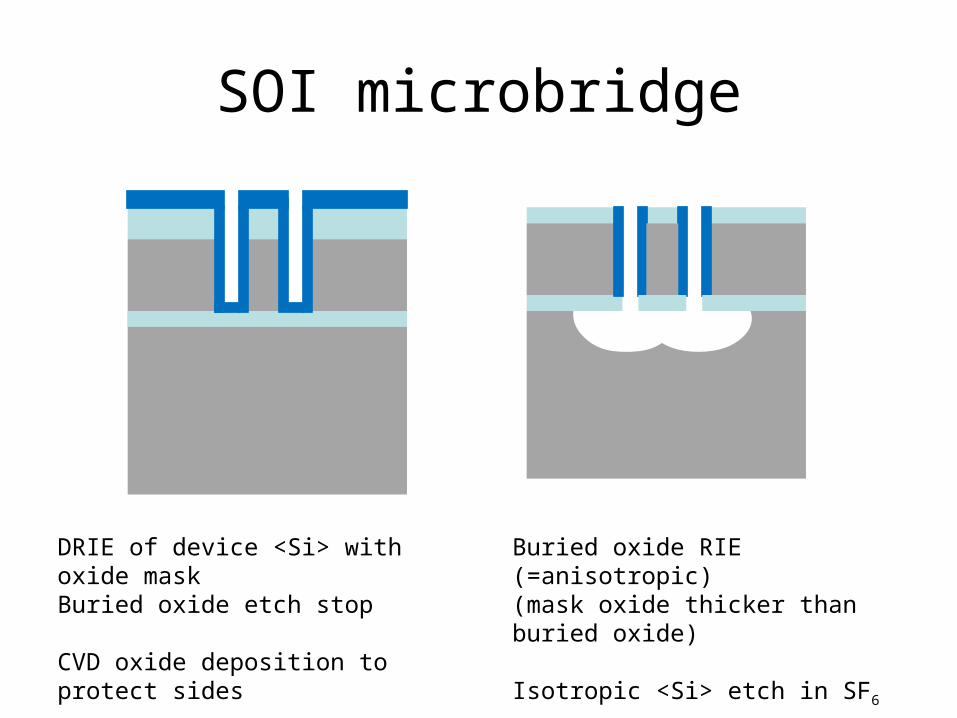
SOI microbridge
DRIE of device <Si> with oxide maskBuried oxide etch stop
CVD oxide deposition to protect sides
Buried oxide RIE (=anisotropic)(mask oxide thicker than buried oxide)
Isotropic <Si> etch in SF6
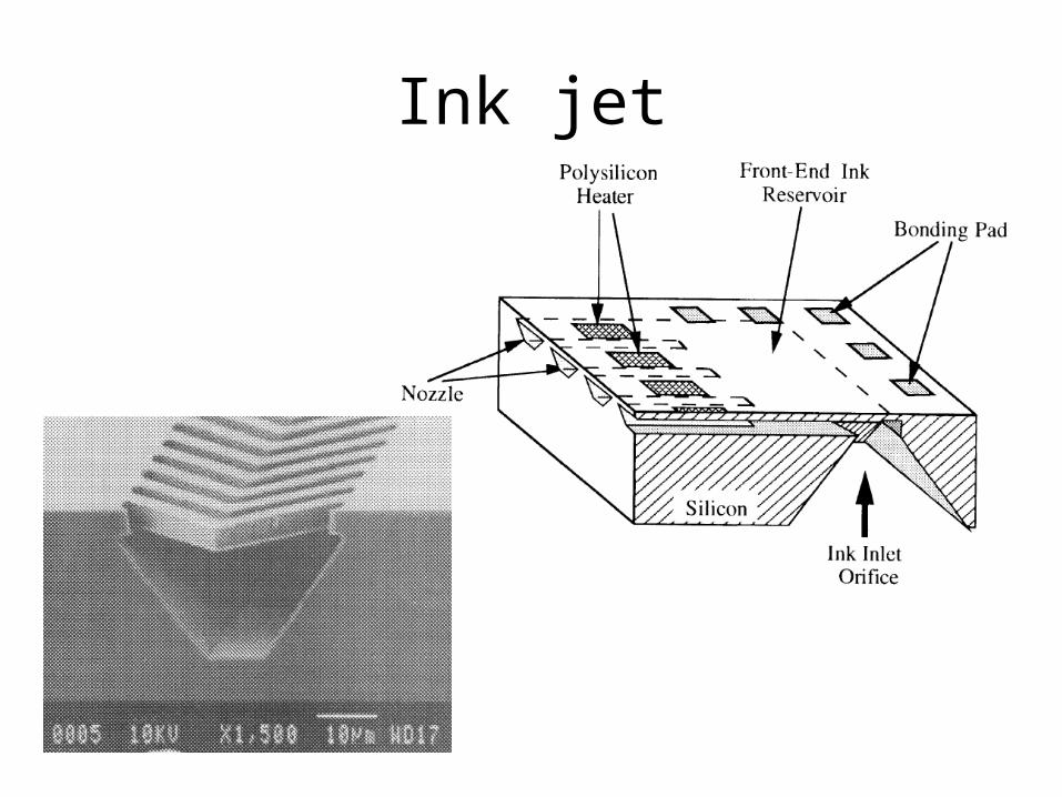
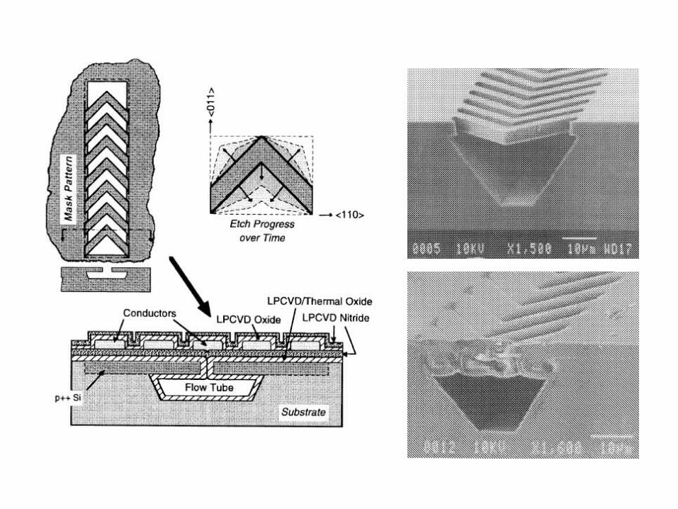
Ink jet


Ink jet (2) Process flow for ink jet: Thermal oxidation, 1 µm thickLitho #1: chip area definitionOxide etchingBoron diffusion, 2 µm deepLitho #2: chevron pattern: 1 µm widthRIE of silicon, 4 µm deepAnisotropic silicon etching to undercut
p++ chevronsThermal oxidationLPCVD nitride deposition for chevron
roof sealingEtchback (or polishing) of nitrideLPCVD polysilicon depositionPoly doping, 20 Ohm/sq
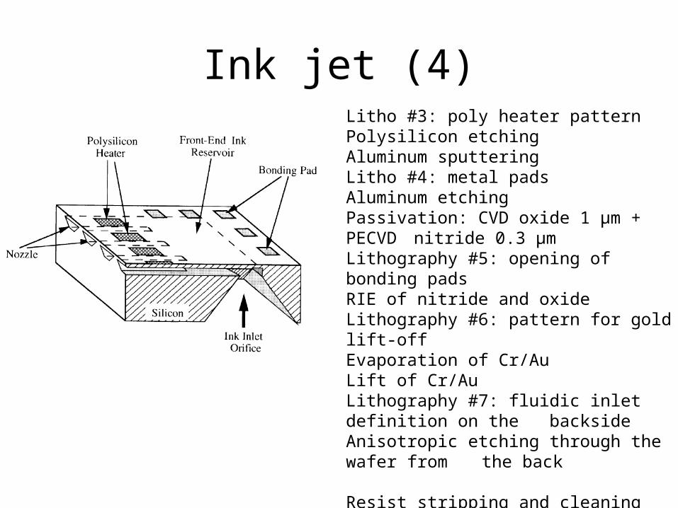
Ink jet (4)Litho #3: poly heater patternPolysilicon etchingAluminum sputteringLitho #4: metal padsAluminum etchingPassivation: CVD oxide 1 µm + PECVD
nitride 0.3 µmLithography #5: opening of bonding padsRIE of nitride and oxideLithography #6: pattern for gold lift-off Evaporation of Cr/Au Lift of Cr/AuLithography #7: fluidic inlet definition on the
backsideAnisotropic etching through the wafer from
the back Resist stripping and cleaning steps omitted
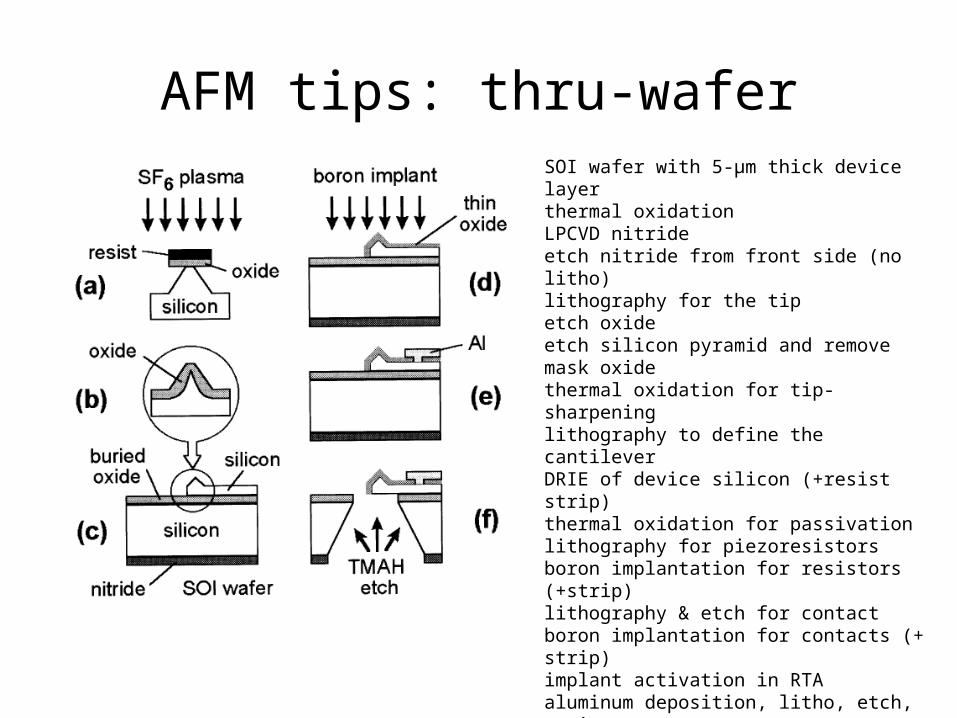
AFM tips: thru-waferSOI wafer with 5-μm thick device layerthermal oxidation LPCVD nitrideetch nitride from front side (no litho)lithography for the tipetch oxideetch silicon pyramid and remove mask oxidethermal oxidation for tip-sharpeninglithography to define the cantilever DRIE of device silicon (+resist strip)thermal oxidation for passivationlithography for piezoresistorsboron implantation for resistors (+strip)lithography & etch for contactboron implantation for contacts (+ strip)implant activation in RTA aluminum deposition, litho, etch, stripFront protection: polyimide spinningbackside nitride litho & etch & stripbackside TMAH anisotropic etch buried oxide etchingpolyimide plasma removal

In-plane vs. out-of-plane needles
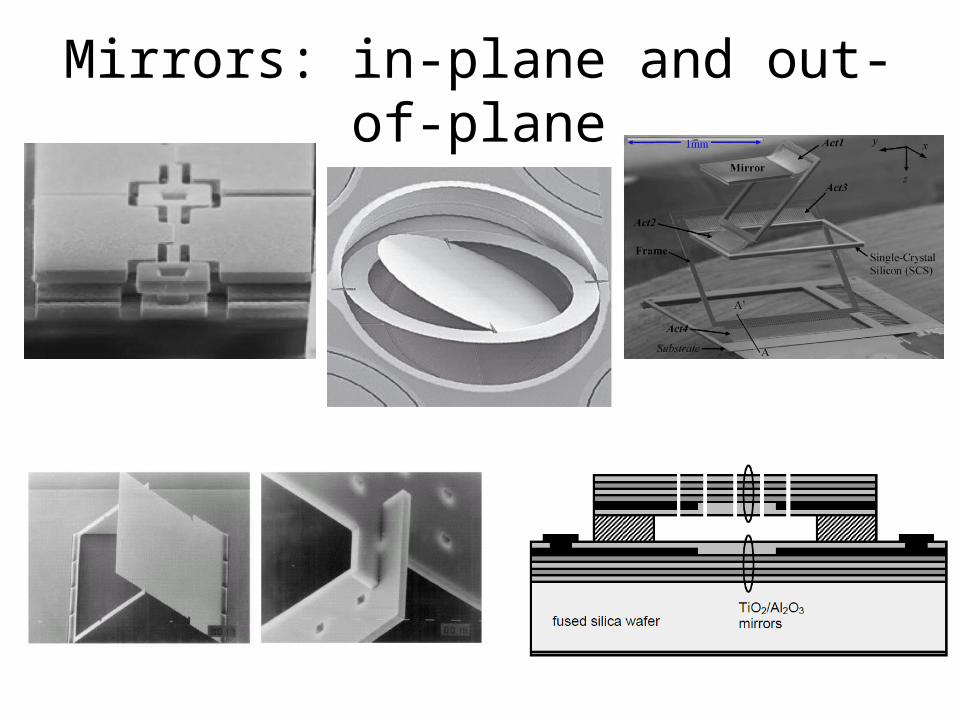
Mirrors: in-plane and out-of-plane
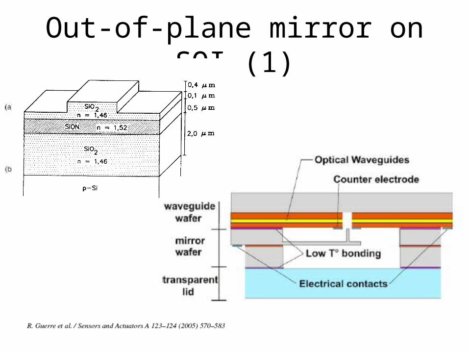
Out-of-plane mirror on SOI (1)
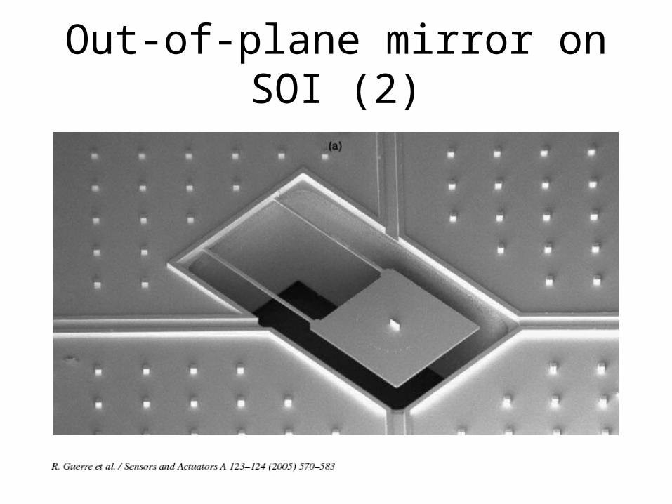
Out-of-plane mirror on SOI (2)

Bonding: critical vs. non-critical
Al
Capacitor gap defined by bonding Microchannel defined by bonding

Bonded microphoneMembrane (top) wafer:Thermal oxidation & oxide patterningNitride deposition & top side nitride etchMembrane metallization (Cr/Au)KOH etch half way
Silicon backplate wafer:OxidationPeeling mask KOH etchingOxidationMetallization (Cr/Au)
Final processing:Gold-gold thermocompression bondingKOH etchingAluminum metallization through shadow mask
Fig. 30.8

Another bonded microphone
Backplate chip with acoustic holes
Membrane chip with Au/Sn solder bumbs
acoustic holes
air gap

IR spectrometer

Integrated accelerometer
Takao, H. et al: A CMOS integrated three-axis accelerometer fabricated with commercial CMOS technology and bulk micromachining, IEEE TED 48 (2001), p. 1961
Anodic bonding: silicon-to-glass
Hermetic cavity (vacuum)

Packaging by capping wafer
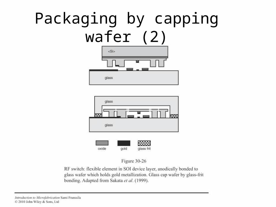
Packaging by capping wafer (2)

Cavity-SOI
oxide Al electrode
Si membrane
ground electrode
air cavity
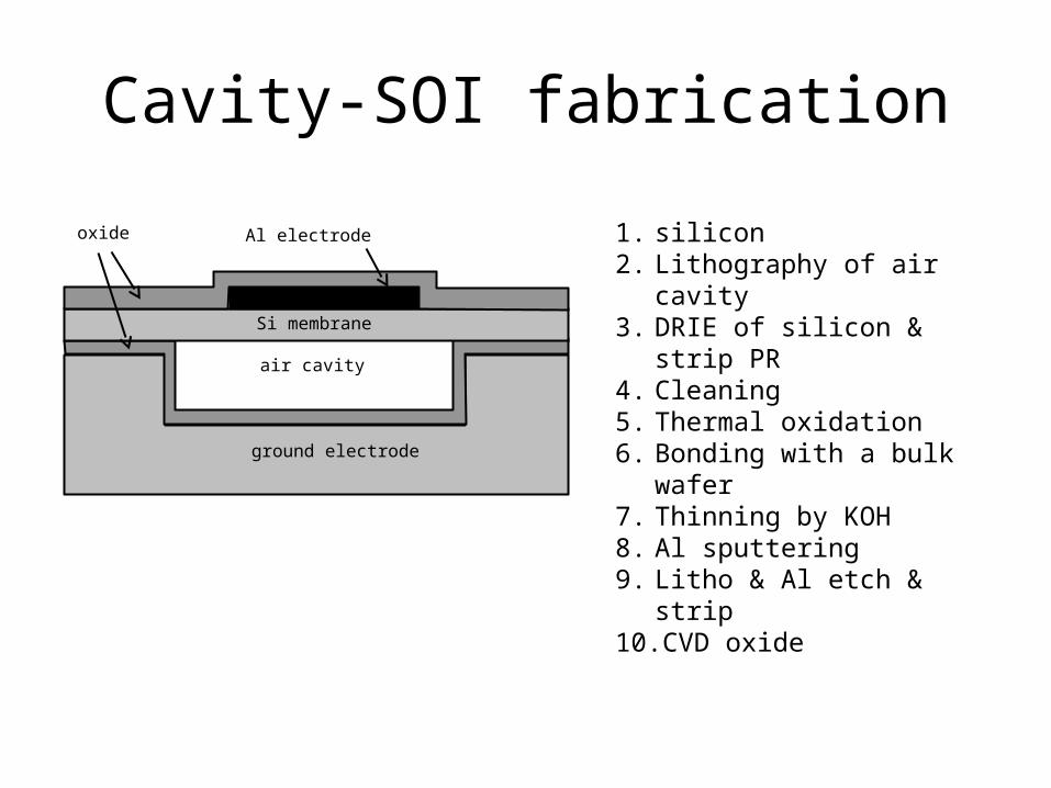
Cavity-SOI fabrication
oxide Al electrode
Si membrane
ground electrode
air cavity
1. silicon2. Lithography of air cavity3. DRIE of silicon & strip PR4. Cleaning5. Thermal oxidation6. Bonding with a bulk wafer7. Thinning by KOH8. Al sputtering9. Litho & Al etch & strip10.CVD oxide
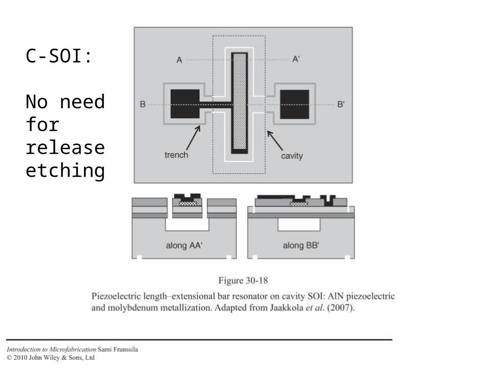
C-SOI:
No need for release etching

CMOS-MEMS integration
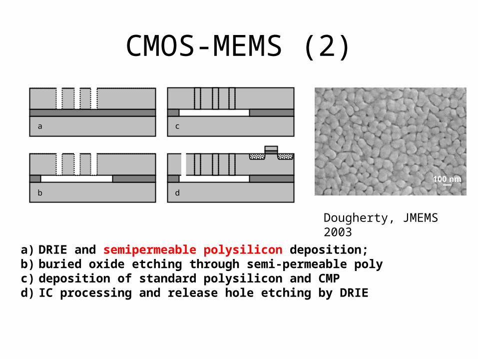
CMOS-MEMS (2)
a
b
c
d
a) DRIE and semipermeable polysilicon deposition; b) buried oxide etching through semi-permeable polyc) deposition of standard polysilicon and CMPd) IC processing and release hole etching by DRIE
Dougherty, JMEMS 2003

CMOS-MEMS
a b
b) single crystal silicon MEMS by backside DRIE
a) thin film MEMS by front side dry plasma release;
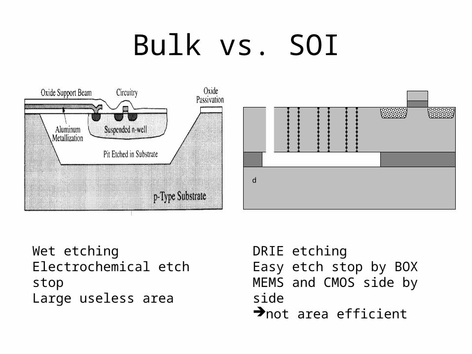
Bulk vs. SOI
d
Wet etchingElectrochemical etch stopLarge useless area
DRIE etchingEasy etch stop by BOXMEMS and CMOS side by sidenot area efficient
SummaryWafer selection: •<100> SSP wafers ?•<100> DSP wafers ?•SOI wafers ?Materials compatibility: •How high temperature does glass wafer tolerate ? •Can cavity-SOI really be processed like standard wafer ?•What are the limitations of piezoelectric materials ?Process-device interactions: •Can thermal diffusion be used or is I/I preferred ?•Is DRIE etch profile ciritical or non-critical•Will the wafers bend due to thin film stresses ?Equipment and process capability:•How can we clean wafers with released structures ?•How thick roof can we deposit ?•Can thick bonded wafer stacks be inserted to wafer boats ?

Summary (2)
Design rules: •What is the smallest allowed linewidth on front side ?•What is the minimum linewidth for backside thru-wafer DRIE ?•What is front-to-back alignment accuracy ?Mask considerations:•Which photomasks are critical, which are non-critical ?•Does etch undercutting need to be compensated on the mask ?Order of process steps:•Should front side processing be completed before backside processing ?•Can any steps be done after thin membrane formation ?•Can any steps be done after thru-wafer holes have been made ?Reliability: •How do stresses build up when more layers are deposited ?•What vacuum does the resonator cavity need ?•What leak rate is allowed in the resonator cavity ?