Brushless DC Motor Controller - TI. · PDF file1features description/ordering information...
24
1FEATURES DESCRIPTION UC2625-EP www.ti.com .................................................................................................................................................................................................. SLUS802 – MARCH 2008 BRUSHLESS DC MOTOR CONTROLLER • Controlled Baseline • Drives Power MOSFETs or Power Darlingtons Directly – One Assembly Site • 50-V Open Collector High-Side Drivers – One Test Site • Latched Soft Start – One Fabrication Site • High-speed Current-Sense Amplifier with Ideal • Extended Temperature Performance of –55°C Diode to 125°C • Pulse-by-Pulse and Average Current Sensing • Enhanced Diminishing Manufacturing Sources (DMS) Support • Over-Voltage and Under-Voltage Protection • Enhanced Product-Change Notification • Direction Latch for Safe Direction Reversal • Qualification Pedigree (1) • Tachometer (1) Component qualification in accordance with JEDEC and • Trimmed Reference Sources 30 mA industry standards to ensure reliable operation over an • Programmable Cross-Conduction Protection extended temperature range. This includes, but is not limited to, Highly Accelerated Stress Test (HAST) or biased 85/85, • Two-Quadrant and Four-Quadrant Operation temperature cycle, autoclave or unbiased HAST, electromigration, bond intermetallic life, and mold compound life. Such qualification testing should not be viewed as justifying use of this component beyond specified performance and environmental limits. The UC2625 motor controller integrates most of the functions required for high-performance brushless dc motor control into one package. When coupled with external power MOSFETs or Darlingtons, this device performs fixed-frequency PWM motor control in either voltage or current mode while implementing closed loop speed control and braking with smart noise rejection, safe direction reversal, and cross-conduction protection. Although specified for operation from power supplies between 10 V and 18 V, the UC2625 can control higher voltage power devices with external level-shifting components. The UC2625 contains fast, high-current push-pull drivers for low-side power devices and 50-V open-collector outputs for high-side power devices or level shifting circuitry. The UC2625 is characterized for operation over the military temperature range of –55°C to 125°C. 1 Please be aware that an important notice concerning availability, standard warranty, and use in critical applications of Texas Instruments semiconductor products and disclaimers thereto appears at the end of this data sheet. PRODUCTION DATA information is current as of publication date. Copyright © 2008, Texas Instruments Incorporated Products conform to specifications per the terms of the Texas Instruments standard warranty. Production processing does not necessarily include testing of all parameters. Copyright © 2008, Texas Instruments Incorporated
Transcript of Brushless DC Motor Controller - TI. · PDF file1features description/ordering information...
1FEATURES
DESCRIPTION
UC2625-EPwww.ti.com .................................................................................................................................................................................................. SLUS802–MARCH 2008
BRUSHLESS DC MOTOR CONTROLLER
• Controlled Baseline • Drives Power MOSFETs or Power DarlingtonsDirectly– One Assembly Site
• 50-V Open Collector High-Side Drivers– One Test Site• Latched Soft Start– One Fabrication Site• High-speed Current-Sense Amplifier with Ideal• Extended Temperature Performance of –55°C
Diodeto 125°C• Pulse-by-Pulse and Average Current Sensing• Enhanced Diminishing Manufacturing Sources
(DMS) Support • Over-Voltage and Under-Voltage Protection• Enhanced Product-Change Notification • Direction Latch for Safe Direction Reversal• Qualification Pedigree (1) • Tachometer(1) Component qualification in accordance with JEDEC and • Trimmed Reference Sources 30 mA
industry standards to ensure reliable operation over an• Programmable Cross-Conduction Protectionextended temperature range. This includes, but is not limited
to, Highly Accelerated Stress Test (HAST) or biased 85/85, • Two-Quadrant and Four-Quadrant Operationtemperature cycle, autoclave or unbiased HAST,electromigration, bond intermetallic life, and mold compoundlife. Such qualification testing should not be viewed asjustifying use of this component beyond specifiedperformance and environmental limits.
The UC2625 motor controller integrates most of the functions required for high-performance brushless dc motorcontrol into one package. When coupled with external power MOSFETs or Darlingtons, this device performsfixed-frequency PWM motor control in either voltage or current mode while implementing closed loop speedcontrol and braking with smart noise rejection, safe direction reversal, and cross-conduction protection.Although specified for operation from power supplies between 10 V and 18 V, the UC2625 can control highervoltage power devices with external level-shifting components. The UC2625 contains fast, high-current push-pulldrivers for low-side power devices and 50-V open-collector outputs for high-side power devices or level shiftingcircuitry.The UC2625 is characterized for operation over the military temperature range of –55°C to 125°C.
1
Please be aware that an important notice concerning availability, standard warranty, and use in critical applications ofTexas Instruments semiconductor products and disclaimers thereto appears at the end of this data sheet.
PRODUCTION DATA information is current as of publication date. Copyright © 2008, Texas Instruments IncorporatedProducts conform to specifications per the terms of the TexasInstruments standard warranty. Production processing does notnecessarily include testing of all parameters.Copyright © 2008, Texas Instruments Incorporated
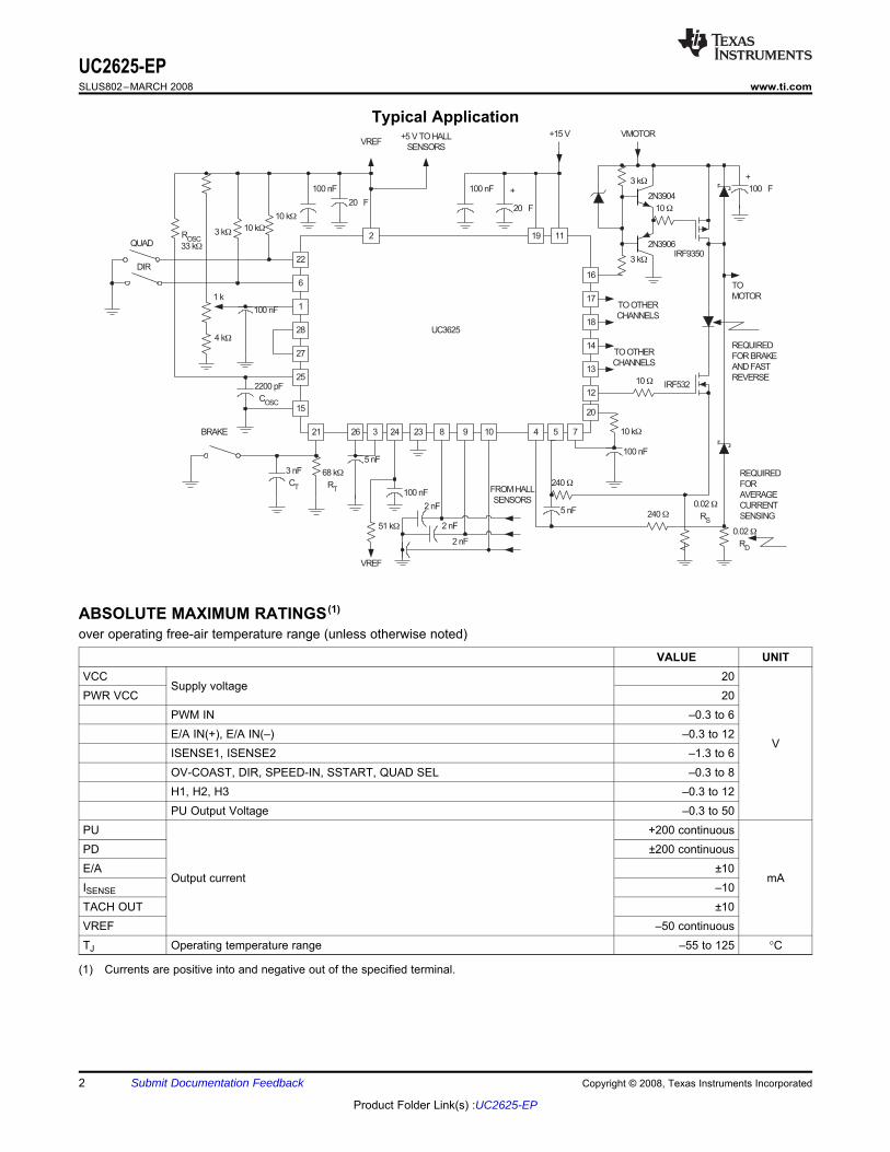
Typical Application
21
27
25
22
6
28
1
15
24326
10 kW
3 kW10 kW
2 19
20
16
11
20 m F
100 nF
20 m F
100 nF +
ROSC
33 kW
2200 pF
COSC
68 kW
RT
3 nF
CT
BRAKE
5 nF
100 nF
23 8 9 10 4 5 7
2 nF
2 nF
2 nF
100 nF
10 kW
5 nF 240 W
240 W
17
18
14
13
12
3 kW
2N3906
100 nF
1 k
4 kW
TOOTHER
CHANNELS
TOOTHER
CHANNELS
10 W
2N3904
10 W
IRF9350
IRF532
3 kW
FROMHALL
SENSORS
VMOTOR+15 V+5 V TOHALL
SENSORSVREF
0.02 W
RS
TO
MOTOR
0.02 W
RD
REQUIRED
FOR
AVERAGE
CURRENT
SENSING
REQUIRED
FOR BRAKE
AND FAST
REVERSE
100 m F
+
UC3625
DIR
QUAD
51 kW
VREF
ABSOLUTE MAXIMUM RATINGS (1)
UC2625-EPSLUS802–MARCH 2008 .................................................................................................................................................................................................. www.ti.com
over operating free-air temperature range (unless otherwise noted)
VALUE UNITVCC 20
Supply voltagePWR VCC 20
PWM IN –0.3 to 6E/A IN(+), E/A IN(–) –0.3 to 12
VISENSE1, ISENSE2 –1.3 to 6OV-COAST, DIR, SPEED-IN, SSTART, QUAD SEL –0.3 to 8H1, H2, H3 –0.3 to 12PU Output Voltage –0.3 to 50
PU +200 continuousPD ±200 continuousE/A ±10
Output current mAISENSE –10TACH OUT ±10VREF –50 continuousTJ Operating temperature range –55 to 125 °C
(1) Currents are positive into and negative out of the specified terminal.
2 Submit Documentation Feedback Copyright © 2008, Texas Instruments Incorporated
Product Folder Link(s) :UC2625-EP
PWR VCC
RC-OSC
PWM IN
E/A OUT
VCC
SSTART
OV-COAST
QUAD SEL
E/A IN(-)
ISENSE
VREF
H3
SPEED-IN
H2
ISENSE1
ISENSE2
DIR
E/A IN(+)
H1
PDC PUB
RC-BRAKE
TACH-OUT
PUA
PDB
PDA GND
PUC
14
13
12
11
10
9
8
7
6
5
4
3
2
1
15
16
17
18
19
20
21
22
23
24
25
26
27
28
UC2625-EPwww.ti.com .................................................................................................................................................................................................. SLUS802–MARCH 2008
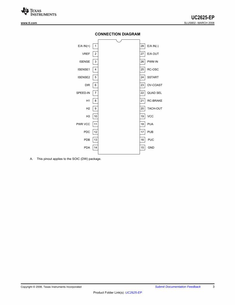
CONNECTION DIAGRAM
A. This pinout applies to the SOIC (DW) package.
Copyright © 2008, Texas Instruments Incorporated Submit Documentation Feedback 3
Product Folder Link(s) :UC2625-EP
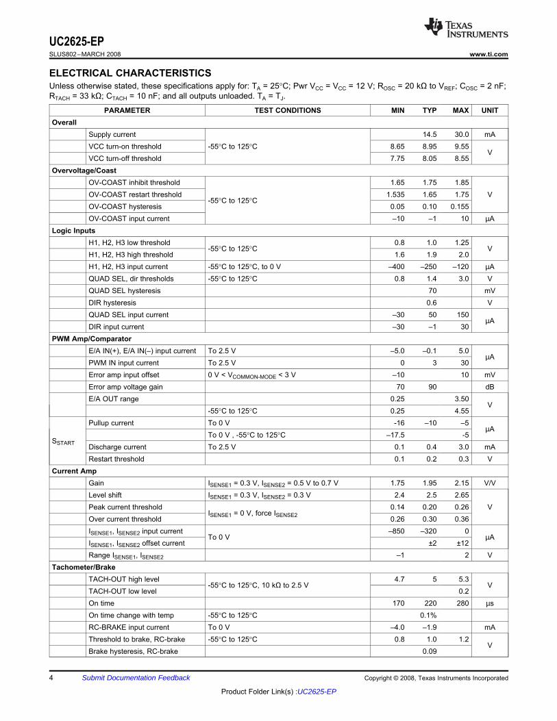
ELECTRICAL CHARACTERISTICS
UC2625-EPSLUS802–MARCH 2008 .................................................................................................................................................................................................. www.ti.com
Unless otherwise stated, these specifications apply for: TA = 25°C; Pwr VCC = VCC = 12 V; ROSC = 20 kΩ to VREF; COSC = 2 nF;RTACH = 33 kΩ; CTACH = 10 nF; and all outputs unloaded. TA = TJ.
PARAMETER TEST CONDITIONS MIN TYP MAX UNITOverall
Supply current 14.5 30.0 mAVCC turn-on threshold -55°C to 125°C 8.65 8.95 9.55
VVCC turn-off threshold 7.75 8.05 8.55
Overvoltage/CoastOV-COAST inhibit threshold 1.65 1.75 1.85OV-COAST restart threshold 1.535 1.65 1.75 V
-55°C to 125°COV-COAST hysteresis 0.05 0.10 0.155OV-COAST input current –10 –1 10 µA
Logic InputsH1, H2, H3 low threshold 0.8 1.0 1.25
-55°C to 125°C VH1, H2, H3 high threshold 1.6 1.9 2.0H1, H2, H3 input current -55°C to 125°C, to 0 V –400 –250 –120 µAQUAD SEL, dir thresholds -55°C to 125°C 0.8 1.4 3.0 VQUAD SEL hysteresis 70 mVDIR hysteresis 0.6 VQUAD SEL input current –30 50 150
µADIR input current –30 –1 30
PWM Amp/ComparatorE/A IN(+), E/A IN(–) input current To 2.5 V –5.0 –0.1 5.0
µAPWM IN input current To 2.5 V 0 3 30Error amp input offset 0 V < VCOMMON-MODE < 3 V –10 10 mVError amp voltage gain 70 90 dBE/A OUT range 0.25 3.50
V-55°C to 125°C 0.25 4.55
Pullup current To 0 V -16 –10 –5µA
To 0 V , -55°C to 125°C –17.5 -5SSTART Discharge current To 2.5 V 0.1 0.4 3.0 mA
Restart threshold 0.1 0.2 0.3 VCurrent Amp
Gain ISENSE1 = 0.3 V, ISENSE2 = 0.5 V to 0.7 V 1.75 1.95 2.15 V/VLevel shift ISENSE1 = 0.3 V, ISENSE2 = 0.3 V 2.4 2.5 2.65Peak current threshold 0.14 0.20 0.26 V
ISENSE1 = 0 V, force ISENSE2Over current threshold 0.26 0.30 0.36ISENSE1, ISENSE2 input current –850 –320 0
To 0 V µAISENSE1, ISENSE2 offset current ±2 ±12Range ISENSE1, ISENSE2 –1 2 V
Tachometer/BrakeTACH-OUT high level 4.7 5 5.3
-55°C to 125°C, 10 kΩ to 2.5 V VTACH-OUT low level 0.2On time 170 220 280 µsOn time change with temp -55°C to 125°C 0.1%RC-BRAKE input current To 0 V –4.0 –1.9 mAThreshold to brake, RC-brake -55°C to 125°C 0.8 1.0 1.2
VBrake hysteresis, RC-brake 0.09
4 Submit Documentation Feedback Copyright © 2008, Texas Instruments Incorporated
Product Folder Link(s) :UC2625-EP
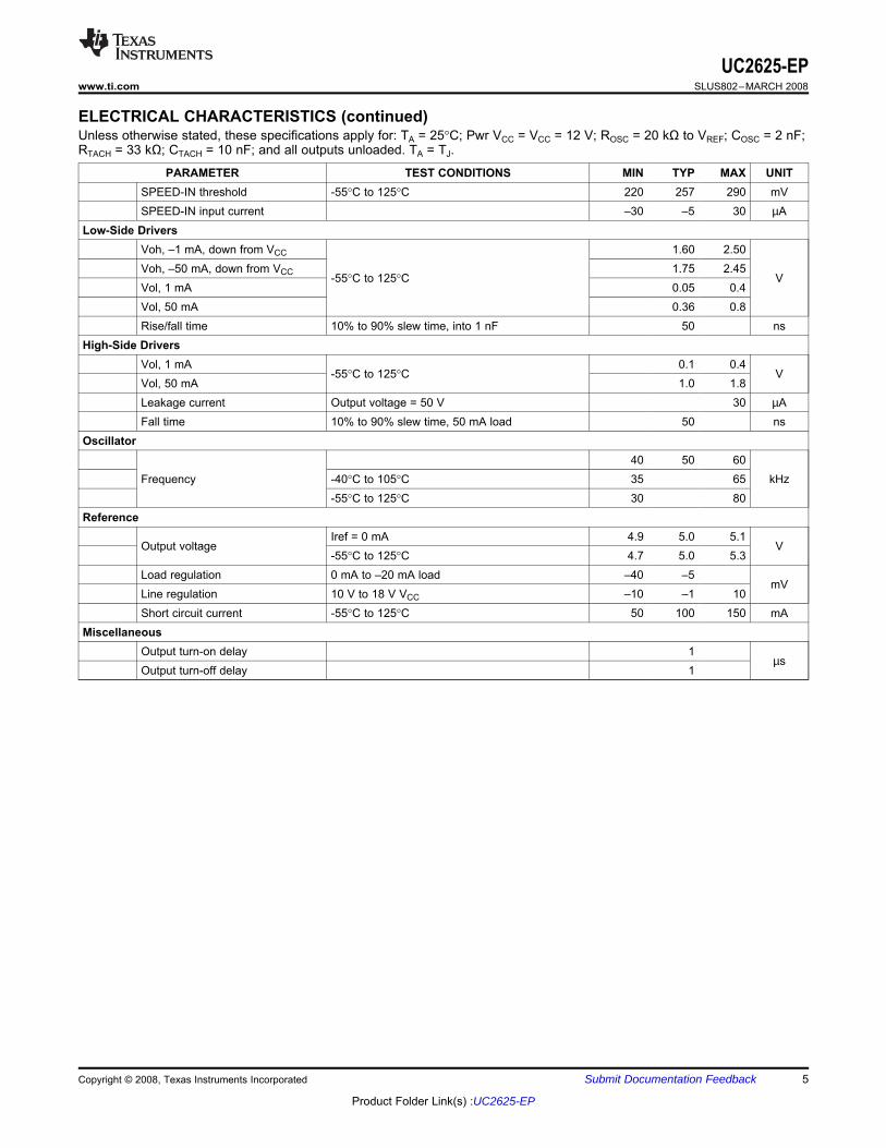
UC2625-EPwww.ti.com .................................................................................................................................................................................................. SLUS802–MARCH 2008
ELECTRICAL CHARACTERISTICS (continued)Unless otherwise stated, these specifications apply for: TA = 25°C; Pwr VCC = VCC = 12 V; ROSC = 20 kΩ to VREF; COSC = 2 nF;RTACH = 33 kΩ; CTACH = 10 nF; and all outputs unloaded. TA = TJ.
PARAMETER TEST CONDITIONS MIN TYP MAX UNITSPEED-IN threshold -55°C to 125°C 220 257 290 mVSPEED-IN input current –30 –5 30 µA
Low-Side DriversVoh, –1 mA, down from VCC 1.60 2.50Voh, –50 mA, down from VCC 1.75 2.45
-55°C to 125°C VVol, 1 mA 0.05 0.4Vol, 50 mA 0.36 0.8Rise/fall time 10% to 90% slew time, into 1 nF 50 ns
High-Side DriversVol, 1 mA 0.1 0.4
-55°C to 125°C VVol, 50 mA 1.0 1.8Leakage current Output voltage = 50 V 30 µAFall time 10% to 90% slew time, 50 mA load 50 ns
Oscillator40 50 60
Frequency -40°C to 105°C 35 65 kHz-55°C to 125°C 30 80
ReferenceIref = 0 mA 4.9 5.0 5.1
Output voltage V-55°C to 125°C 4.7 5.0 5.3
Load regulation 0 mA to –20 mA load –40 –5mV
Line regulation 10 V to 18 V VCC –10 –1 10Short circuit current -55°C to 125°C 50 100 150 mA
MiscellaneousOutput turn-on delay 1
µsOutput turn-off delay 1
Copyright © 2008, Texas Instruments Incorporated Submit Documentation Feedback 5
Product Folder Link(s) :UC2625-EP
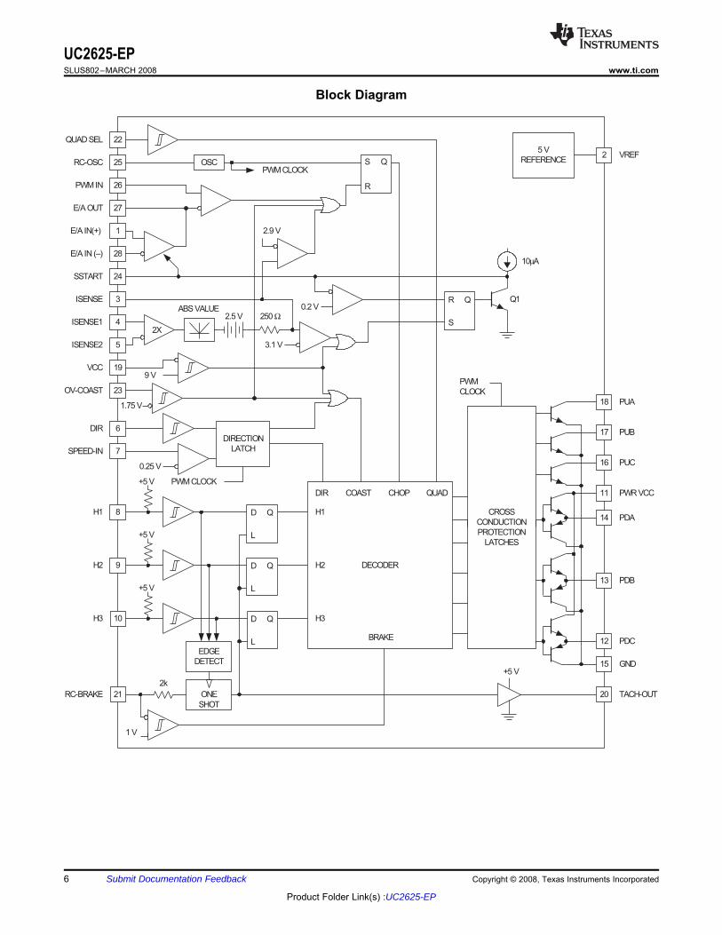
Block Diagram
22
26
252
QUAD SEL
RC-OSC
PWMIN
27
28
1
E/A OUT
E/A IN(+)
E/A IN (–)
OSC S Q
R
S
QR
PWMCLOCK
24SSTART
3ISENSE
4ISENSE1
5ISENSE2
19VCC
23OV-COAST
6DIR
7SPEED-IN
2X
2.5 V 250 Ω
2.9 V
Q1
10µA
3.1 V
9 V
DIRECTION
LATCH
0.25 V
PWMCLOCK
8H1
9H2
L
QD
L
QD
L
QD10H3
+5 V
+5 V
+5 V
EDGE
DETECT
ONE
SHOT
21RC-BRAKE
2k
1 V
DIR COAST CHOP QUAD
H2
H1
H3
BRAKE
DECODER
CROSS
CONDUCTION
PROTECTION
LATCHES
18 PUA
17 PUB
16 PUC
14 PDA
13 PDB
12 PDC
15 GND
20 TACH-OUT
11 PWR VCC
+5 V
VREF5 V
REFERENCE
PWM
CLOCK
1.75 V
ABS VALUE 0.2 V
UC2625-EPSLUS802–MARCH 2008 .................................................................................................................................................................................................. www.ti.com
6 Submit Documentation Feedback Copyright © 2008, Texas Instruments Incorporated
Product Folder Link(s) :UC2625-EP
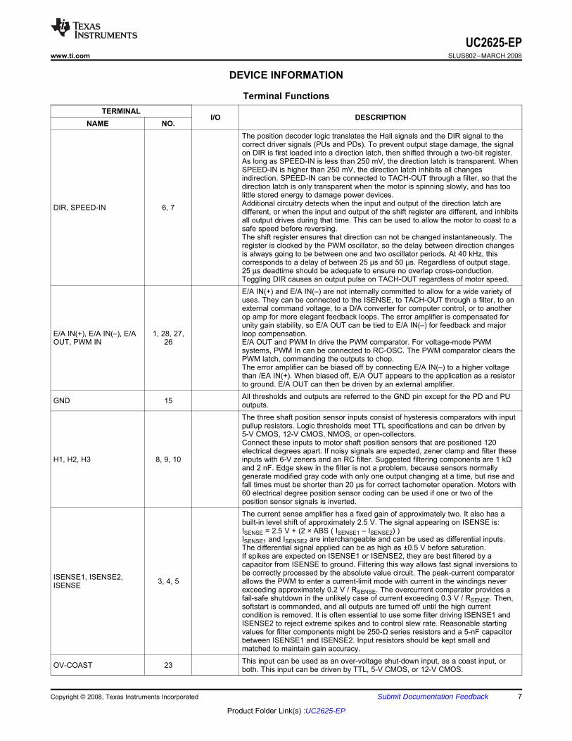
DEVICE INFORMATION
UC2625-EPwww.ti.com .................................................................................................................................................................................................. SLUS802–MARCH 2008
Terminal FunctionsTERMINAL
I/O DESCRIPTIONNAME NO.
The position decoder logic translates the Hall signals and the DIR signal to thecorrect driver signals (PUs and PDs). To prevent output stage damage, the signalon DIR is first loaded into a direction latch, then shifted through a two-bit register.As long as SPEED-IN is less than 250 mV, the direction latch is transparent. WhenSPEED-IN is higher than 250 mV, the direction latch inhibits all changesindirection. SPEED-IN can be connected to TACH-OUT through a filter, so that thedirection latch is only transparent when the motor is spinning slowly, and has toolittle stored energy to damage power devices.Additional circuitry detects when the input and output of the direction latch areDIR, SPEED-IN 6, 7 different, or when the input and output of the shift register are different, and inhibitsall output drives during that time. This can be used to allow the motor to coast to asafe speed before reversing.The shift register ensures that direction can not be changed instantaneously. Theregister is clocked by the PWM oscillator, so the delay between direction changesis always going to be between one and two oscillator periods. At 40 kHz, thiscorresponds to a delay of between 25 µs and 50 µs. Regardless of output stage,25 µs deadtime should be adequate to ensure no overlap cross-conduction.Toggling DIR causes an output pulse on TACH-OUT regardless of motor speed.E/A IN(+) and E/A IN(–) are not internally committed to allow for a wide variety ofuses. They can be connected to the ISENSE, to TACH-OUT through a filter, to anexternal command voltage, to a D/A converter for computer control, or to anotherop amp for more elegant feedback loops. The error amplifier is compensated forunity gain stability, so E/A OUT can be tied to E/A IN(–) for feedback and major
E/A IN(+), E/A IN(–), E/A 1, 28, 27, loop compensation.OUT, PWM IN 26 E/A OUT and PWM In drive the PWM comparator. For voltage-mode PWM
systems, PWM In can be connected to RC-OSC. The PWM comparator clears thePWM latch, commanding the outputs to chop.The error amplifier can be biased off by connecting E/A IN(–) to a higher voltagethan /EA IN(+). When biased off, E/A OUT appears to the application as a resistorto ground. E/A OUT can then be driven by an external amplifier.All thresholds and outputs are referred to the GND pin except for the PD and PUGND 15 outputs.The three shaft position sensor inputs consist of hysteresis comparators with inputpullup resistors. Logic thresholds meet TTL specifications and can be driven by5-V CMOS, 12-V CMOS, NMOS, or open-collectors.Connect these inputs to motor shaft position sensors that are positioned 120electrical degrees apart. If noisy signals are expected, zener clamp and filter these
H1, H2, H3 8, 9, 10 inputs with 6-V zeners and an RC filter. Suggested filtering components are 1 kΩand 2 nF. Edge skew in the filter is not a problem, because sensors normallygenerate modified gray code with only one output changing at a time, but rise andfall times must be shorter than 20 µs for correct tachometer operation. Motors with60 electrical degree position sensor coding can be used if one or two of theposition sensor signals is inverted.The current sense amplifier has a fixed gain of approximately two. It also has abuilt-in level shift of approximately 2.5 V. The signal appearing on ISENSE is:ISENSE = 2.5 V + (2 × ABS ( ISENSE1 – ISENSE2) )ISENSE1 and ISENSE2 are interchangeable and can be used as differential inputs.The differential signal applied can be as high as ±0.5 V before saturation.If spikes are expected on ISENSE1 or ISENSE2, they are best filtered by acapacitor from ISENSE to ground. Filtering this way allows fast signal inversions tobe correctly processed by the absolute value circuit. The peak-current comparatorISENSE1, ISENSE2, 3, 4, 5 allows the PWM to enter a current-limit mode with current in the windings neverISENSE exceeding approximately 0.2 V / RSENSE. The overcurrent comparator provides afail-safe shutdown in the unlikely case of current exceeding 0.3 V / RSENSE. Then,softstart is commanded, and all outputs are turned off until the high currentcondition is removed. It is often essential to use some filter driving ISENSE1 andISENSE2 to reject extreme spikes and to control slew rate. Reasonable startingvalues for filter components might be 250-Ω series resistors and a 5-nF capacitorbetween ISENSE1 and ISENSE2. Input resistors should be kept small andmatched to maintain gain accuracy.This input can be used as an over-voltage shut-down input, as a coast input, orOV-COAST 23 both. This input can be driven by TTL, 5-V CMOS, or 12-V CMOS.
Copyright © 2008, Texas Instruments Incorporated Submit Documentation Feedback 7
Product Folder Link(s) :UC2625-EP
UC2625-EPSLUS802–MARCH 2008 .................................................................................................................................................................................................. www.ti.com
Terminal Functions (continued)TERMINAL
I/O DESCRIPTIONNAME NO.
These outputs can drive the gates of N-channel power MOSFETs directly or theycan drive the bases of power Darlingtons if some form of current limiting is used.They are meant to drive low-side power devices in high-current output stages.
PDA, PDB, PDC 12, 13, 14 Current available from these pins can peak as high as 0.5 A. These outputs featurea true totem-pole output stage. Beware of exceeding device power dissipationlimits when using these outputs for high continuous currents. These outputs pullhigh to turn a “low-side” device on (active high).These outputs are open-collector, high-voltage drivers that are meant to drivehigh-side power devices in high-current output stages. These are active lowoutputs, meaning that these outputs pull low to command a high-side device on.These outputs can drive low-voltage PNP Darlingtons and P-channel MOSFETsPUA, PUB, PUC 16, 17, 18 directly, and can drive any high-voltage device using external charge pumptechniques, transformer signal coupling, cascode level-shift transistors, oropto-isolated drive (high-speed opto devices are recommended). (Seeapplications).This supply pin carries the current sourced by the PD outputs. When connectingPD outputs directly to the bases of power Darlingtons, the PWR VCC pin can bePWR VCC 11 current limited with a resistor. Darlington outputs can also be "Baker Clamped" withdiodes from collectors back to PWR VCC. (See Applications)The device can chop power devices in either of two modes, referred to as“two-quadrant” (Quad Sellow) and “four quadrant” (Quad Sel high). Whentwo-quadrant chopping, the pulldown power devices are chopped by the output ofthe PWM latch while the pullup drivers remain on. The load chops into onecommutation diode, and except for back-EMF, will exhibit slow discharge currentand faster charge current. Two-quadrant chopping can be more efficient thanQUAD SEL 22 four-quadrant.When four-quadrant chopping, all power drivers are chopped by the PWM latch,causing the load current to flow into two diodes during chopping. This modeexhibits better control of load current when current is low, and is preferred in servosystems for equal control over acceleration and deceleration. The QUAD SEL inputhas no effect on operation during braking.Each time the TACH-OUT pulses, the capacitor tied to RC-BRAKE dischargesfrom approximately 3.33 V down to 1.67 V through a resistor. The tachometerpulse width is approximately T = 0.67 RT CT, where RT and CT are a resistor andcapacitor from RC-BRAKE to ground. Recommended values for RT are 10 kΩ to500 kΩ, and recommended values for CT are 1 nF to 100 nF, allowing timesbetween 5 µs and 10 ms. Best accuracy and stability are achieved with values inthe centers of those ranges.RC-BRAKE also has another function. If RC-BRAKE pin is pulled below the brake
RC-BRAKE 21 threshold, the device enters brake mode. This mode consists of turning off all threehigh-side devices, enabling all three low-side devices, and disabling thetachometer. The only things that inhibit low-side device operation in braking arelow-supply, exceeding peak current, OV-COAST command, and the PWMcomparator signal. The last of these means that if current sense is implementedsuch that the signal in the current sense amplifier is proportional to braking current,the low-side devices will brake the motor with current control. (See applications)Simpler current sense connections results in uncontrolled braking and potentialdamage to the power devices.The UC3625 can regulate motor current using fixed-frequency pulse widthmodulation (PWM). The RC-OSC pin sets oscillator frequency by means of timingresistor ROSC from the RC-OSC pin to VREF and capacitor COSC from RC-OSCto Gnd. Resistors 10 kΩ to 100 kΩ and capacitors 1 nF to 100 nF works the best,but frequency should always be below 500 kHz. Oscillator frequency isapproximately:
RC-OSC 25 F = 2/(ROSC x COSC )Additional components can be added to this device to cause it to operate as afixed off-time PWM rather than a fixed frequency PWM, using the RC-OSC pin toselect the monostable time constant.The voltage on the RC-OSC pin is normally a ramp of about 1.2 V peak-to-peak,centered at approximately 1.6 V. This ramp can be used for voltage-mode PWMcontrol, or can be used for slope compensation in current-mode control.
8 Submit Documentation Feedback Copyright © 2008, Texas Instruments Incorporated
Product Folder Link(s) :UC2625-EP
UC2625-EPwww.ti.com .................................................................................................................................................................................................. SLUS802–MARCH 2008
Terminal Functions (continued)TERMINAL
I/O DESCRIPTIONNAME NO.
Any time that VCC drops below threshold or the sensed current exceeds theover-current threshold, the soft-start latch is set. When set, it turns on a transistorthat pulls down on SSTART. Normally, a capacitor is connected to this pin, and thetransistor will completely discharge the capacitor. A comparator senses when theNPN transistor has completely discharged the capacitor, and allows the soft-startlatch to clear when the fault is removed. When the fault is removed, the soft-startcapacitor charges from the on-chip current source.SSTART clamps the output of the error amplifier, not allowing the error amplifierSSTART 24 output voltage to exceed SSTART regardless of input. The ramp on RC-OSC canbe applied to PWM In and compared to E/A OUT. With SSTART discharged below0.2 V and the ramp minimum being approximately 1.0 V, the PWM comparatorkeeps the PWM latch cleared and the outputs off. As SSTART rises, the PWMcomparator begins to duty-cycle modulate the PWM latch until the error amplifierinputs overcome the clamp. This provides for a safe and orderly motor start-upfrom an off or fault condition. A 51-kΩ resister is added between VREF andSSTART to ensure switching.Any change in the H1, H2, or H3 inputs loads data from these inputs into theposition sensor latches. At the same time data is loaded, a fixed-width 5-V pulse istriggered on TACH-OUT. The average value of the voltage on TACH-OUT isdirectly proportional to speed, so this output can be used as a true tachometer forspeed feedback with an external filter or averaging circuit which usually consists of
TACH-OUT 20 a resistor and capacitor.Whenever TACH-OUT is high, the position latches are inhibited, such that duringthe noisiest part of the commutation cycle, additional commutations are notpossible. Although this effectively sets a maximum rotational speed, the maximumspeed can be set above the highest expected speed, preventing false commutationand chatter.This device operates with supplies between 10 V and 18 V. Under-voltage lockoutkeeps all outputs off below 7.5 V, insuring that the output transistors never turn on
VCC 19 until full drive capability is available. Bypass VCC to ground with an 0.1-µF ceramiccapacitor. Using a 10-µF electrolytic bypass capacitor as well can be beneficial inapplications with high supply impedance.This pin provides regulated 5 V for driving Hall-effect devices and speed controlcircuitry. VREF reaches 5 V before VCC enables, ensuring that Hall-effect devices
VREF 2 powered from VREF becomes active before the UC3625 drives any output. Forproper performance VREF should be bypassed with at least a 0.1-µF capacitor toground.
Copyright © 2008, Texas Instruments Incorporated Submit Documentation Feedback 9
Product Folder Link(s) :UC2625-EP
TYPICAL CHARACTERISTICS
On
Tim
e0.001
CT – F
0.01 0.11 s
10 s
100 s
10 ms
1 ms
100 ms
RT – 10 kRT – 30 k
RT – 100 kRT – 500 k
0.001 0.01 0.1100 Hz
1 kHz
10 kHz
100 kHz
1 MHz
Osc
illat
or
Fre
qu
ency
COSC (F)
ROSC – 10 k
ROSC – 10 k
ROSC – 100 k
-75
Temperature – C
-50 -25 0 755025 125100
Sup
ply
Cur
rent
– m
A
0
2
4
6
8
10
12
14
16
18
20
-75
Temperature – C
-50 -25 0 755025 125100
Sof
t Sta
rt C
urre
nt –
A
-15
-14
-13
-12
-11
-10
-9
-8
-7
-6
-5
UC2625-EPSLUS802–MARCH 2008 .................................................................................................................................................................................................. www.ti.com
Oscillator Frequency Tachometer on Timevs vs
COSC and ROSC RT and CT
Figure 1. Figure 2.
Supply Current Soft-Start Pullup Currentvs vs
Temperature Temperature
Figure 3. Figure 4.
10 Submit Documentation Feedback Copyright © 2008, Texas Instruments Incorporated
Product Folder Link(s) :UC2625-EP
-75
Temperature – C
-50 -25 0 755025 125100
Sof
t Sta
rt C
urre
nt –
mA
0
.25
.50
.75
1.00
1.25
ISENSE2 – ISENSE1 – V
I SE
NS
E –
V
0.50.0-0.52.5
3
3.5
UC2625-EPwww.ti.com .................................................................................................................................................................................................. SLUS802–MARCH 2008
TYPICAL CHARACTERISTICS (continued)
Soft-Start Discharge Current Current Sense Amplifier Transfer Functionvs vs
Temperature ISENSE2 – ISENSE1
Figure 5. Figure 6.
Copyright © 2008, Texas Instruments Incorporated Submit Documentation Feedback 11
Product Folder Link(s) :UC2625-EP
APPLICATION INFORMATION
Cross Conduction Prevention
EDGE
FINDER
SHIFT
REGS Q
QR
S Q
QR
PUA
PDAPULL
DOWN
PULL UP
FROM
DECODER
PWM
CLK
UC2625-EPSLUS802–MARCH 2008 .................................................................................................................................................................................................. www.ti.com
The UC2625 inserts delays to prevent cross conduction due to overlapping drive signals. However, some thoughtmust always be given to cross conduction in output stage design because no amount of dead time can preventfast slewing signals from coupling drive to a power device through a parasitic capacitance.The UC2625 contains input latches that serve as noise blanking filters. These latches remain transparent throughany phase of a motor rotation and latch immediately after an input transition is detected. They remain latched fortwo cycles of the PWM oscillator. At a PWM oscillator speed of 20 kHz, this corresponds to 50 µs to 100 µs ofblank time which limits maximum rotational speed to 100 kRPM for a motor with six transitions per rotation or 50kRPM for a motor with 12 transitions per rotation.This prevents noise generated in the first 50 µs of a transition from propagating to the output transistors andcausing cross-conduction or chatter.The UC2625 also contains six flip flops corresponding to the six output drive signals. One of these flip flops is setevery time that an output drive signal is turned on, and cleared two PWM oscillator cycles after that drive signalis turned off. The output of each flip flop is used to inhibit drive to the opposing output (Figure 7). In this way, it isimpossible to turn on driver PUA and PDA at the same time. It is also impossible for one of these drivers to turnon without the other driver having been off for at least two PWM oscillator clocks.
Figure 7. Cross Conduction Prevention
12 Submit Documentation Feedback Copyright © 2008, Texas Instruments Incorporated
Product Folder Link(s) :UC2625-EP
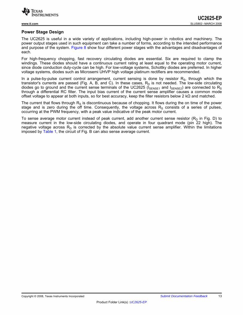
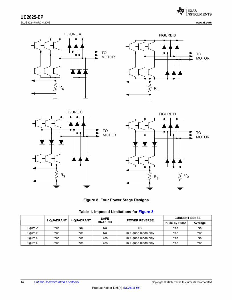
Power Stage Design
UC2625-EPwww.ti.com .................................................................................................................................................................................................. SLUS802–MARCH 2008
The UC2625 is useful in a wide variety of applications, including high-power in robotics and machinery. Thepower output stages used in such equipment can take a number of forms, according to the intended performanceand purpose of the system. Figure 8 show four different power stages with the advantages and disadvantages ofeach.For high-frequency chopping, fast recovery circulating diodes are essential. Six are required to clamp thewindings. These diodes should have a continuous current rating at least equal to the operating motor current,since diode conduction duty-cycle can be high. For low-voltage systems, Schottky diodes are preferred. In highervoltage systems, diodes such as Microsemi UHVP high voltage platinum rectifiers are recommended.In a pulse-by-pulse current control arrangement, current sensing is done by resistor RS, through which thetransistor's currents are passed (Fig. A, B, and C). In these cases, RD is not needed. The low-side circulatingdiodes go to ground and the current sense terminals of the UC2625 (ISENSE1 and ISENSE2) are connected to RSthrough a differential RC filter. The input bias current of the current sense amplifier causes a common modeoffset voltage to appear at both inputs, so for best accuracy, keep the filter resistors below 2 kΩ and matched.The current that flows through RS is discontinuous because of chopping. It flows during the on time of the powerstage and is zero during the off time. Consequently, the voltage across RS consists of a series of pulses,occurring at the PWM frequency, with a peak value indicative of the peak motor current.To sense average motor current instead of peak current, add another current sense resistor (RD in Fig. D) tomeasure current in the low-side circulating diodes, and operate in four quadrant mode (pin 22 high). Thenegative voltage across RD is corrected by the absolute value current sense amplifier. Within the limitationsimposed by Table 1, the circuit of Fig. B can also sense average current.
Copyright © 2008, Texas Instruments Incorporated Submit Documentation Feedback 13
Product Folder Link(s) :UC2625-EP
TO
MOTOR
RS
FIGURE A
TO
MOTOR
RS
FIGURE B
TO
MOTOR
RS
FIGURE C
TO
MOTOR
RS
RD
FIGURE D
UC2625-EPSLUS802–MARCH 2008 .................................................................................................................................................................................................. www.ti.com
Figure 8. Four Power Stage Designs
Table 1. Imposed Limitations for Figure 8CURRENT SENSESAFE2 QUADRANT 4 QUADRANT POWER REVERSEBRAKING Pulse-by-Pulse Average
Figure A Yes No No N0 Yes NoFigure B Yes Yes No In 4-quad mode only Yes YesFigure C Yes Yes Yes In 4-quad mode only Yes NoFigure D Yes Yes Yes In 4-quad mode only Yes Yes
14 Submit Documentation Feedback Copyright © 2008, Texas Instruments Incorporated
Product Folder Link(s) :UC2625-EP
UC2625-EPwww.ti.com .................................................................................................................................................................................................. SLUS802–MARCH 2008
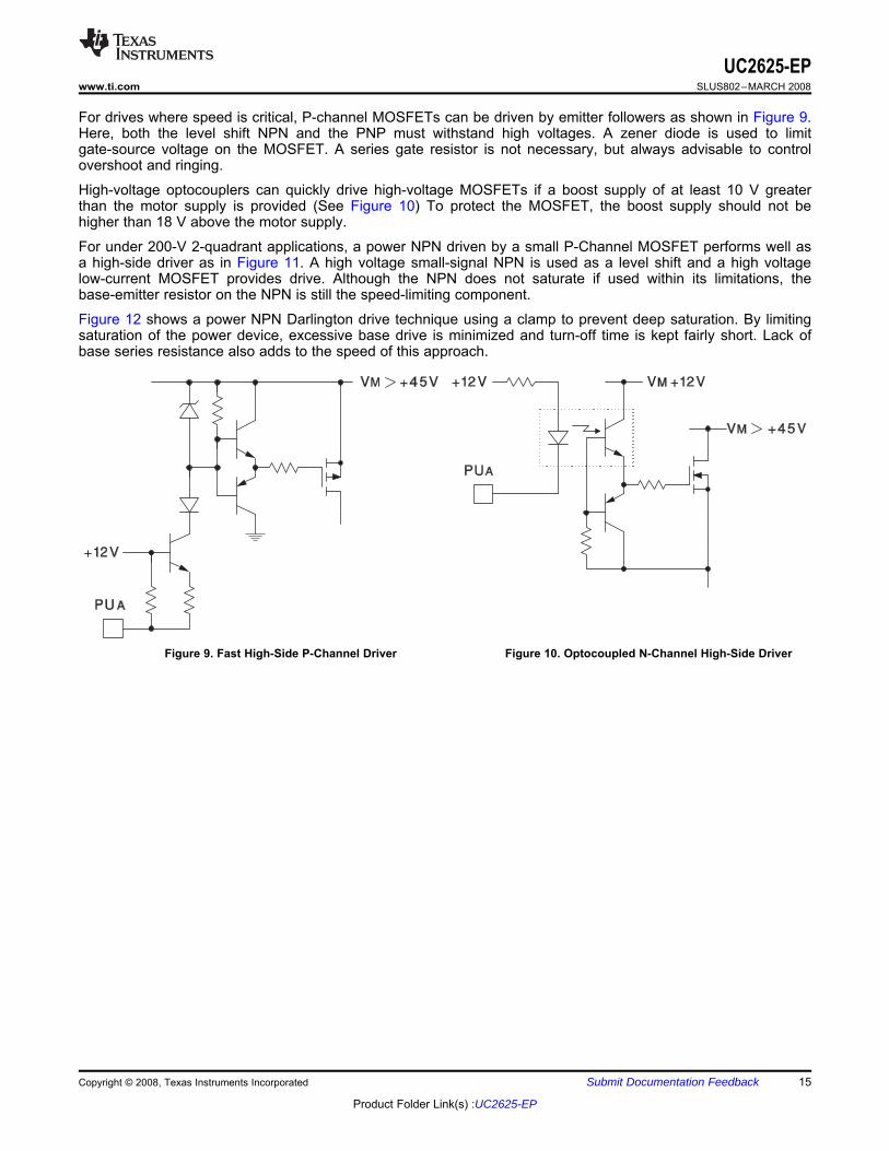
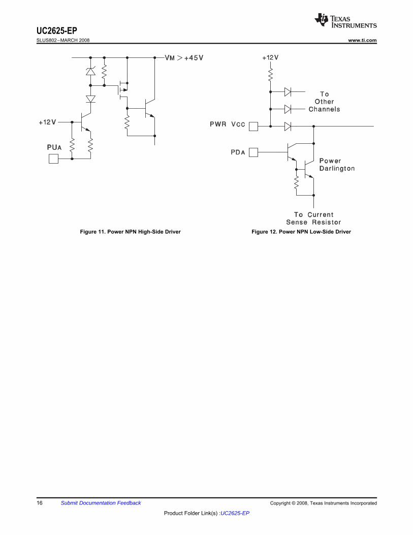
For drives where speed is critical, P-channel MOSFETs can be driven by emitter followers as shown in Figure 9.Here, both the level shift NPN and the PNP must withstand high voltages. A zener diode is used to limitgate-source voltage on the MOSFET. A series gate resistor is not necessary, but always advisable to controlovershoot and ringing.High-voltage optocouplers can quickly drive high-voltage MOSFETs if a boost supply of at least 10 V greaterthan the motor supply is provided (See Figure 10) To protect the MOSFET, the boost supply should not behigher than 18 V above the motor supply.For under 200-V 2-quadrant applications, a power NPN driven by a small P-Channel MOSFET performs well asa high-side driver as in Figure 11. A high voltage small-signal NPN is used as a level shift and a high voltagelow-current MOSFET provides drive. Although the NPN does not saturate if used within its limitations, thebase-emitter resistor on the NPN is still the speed-limiting component.Figure 12 shows a power NPN Darlington drive technique using a clamp to prevent deep saturation. By limitingsaturation of the power device, excessive base drive is minimized and turn-off time is kept fairly short. Lack ofbase series resistance also adds to the speed of this approach.
Figure 9. Fast High-Side P-Channel Driver Figure 10. Optocoupled N-Channel High-Side Driver
Copyright © 2008, Texas Instruments Incorporated Submit Documentation Feedback 15
Product Folder Link(s) :UC2625-EP
UC2625-EPSLUS802–MARCH 2008 .................................................................................................................................................................................................. www.ti.com
Figure 11. Power NPN High-Side Driver Figure 12. Power NPN Low-Side Driver
16 Submit Documentation Feedback Copyright © 2008, Texas Instruments Incorporated
Product Folder Link(s) :UC2625-EP
Fast High-Side N-Channel Driver with Transformer Isolation
28
7
1
6
5
4
31
2
6
7
48
UC3724N UC3725N
1:2
PUA
33kW
3
+12V
1nF5kW 100nF
VMOTOR
TO MOTOR
UC2625-EPwww.ti.com .................................................................................................................................................................................................. SLUS802–MARCH 2008
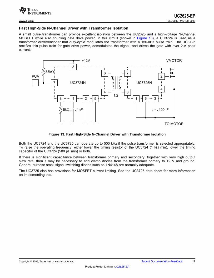
A small pulse transformer can provide excellent isolation between the UC2625 and a high-voltage N-ChannelMOSFET while also coupling gate drive power. In this circuit (shown in Figure 13), a UC3724 is used as atransformer driver/encoder that duty-cycle modulates the transformer with a 150-kHz pulse train. The UC3725rectifies this pulse train for gate drive power, demodulates the signal, and drives the gate with over 2-A peakcurrent.
Figure 13. Fast High-Side N-Channel Driver with Transformer Isolation
Both the UC3724 and the UC3725 can operate up to 500 kHz if the pulse transformer is selected appropriately.To raise the operating frequency, either lower the timing resistor of the UC3724 (1 kΩ min), lower the timingcapacitor of the UC3724 (500 pF min) or both.If there is significant capacitance between transformer primary and secondary, together with very high outputslew rate, then it may be necessary to add clamp diodes from the transformer primary to 12 V and ground.General purpose small signal switching diodes such as 1N4148 are normally adequate.The UC3725 also has provisions for MOSFET current limiting. See the UC3725 data sheet for more informationon implementing this.
Copyright © 2008, Texas Instruments Incorporated Submit Documentation Feedback 17
Product Folder Link(s) :UC2625-EP
Computational Truth Table
UC2625-EPSLUS802–MARCH 2008 .................................................................................................................................................................................................. www.ti.com
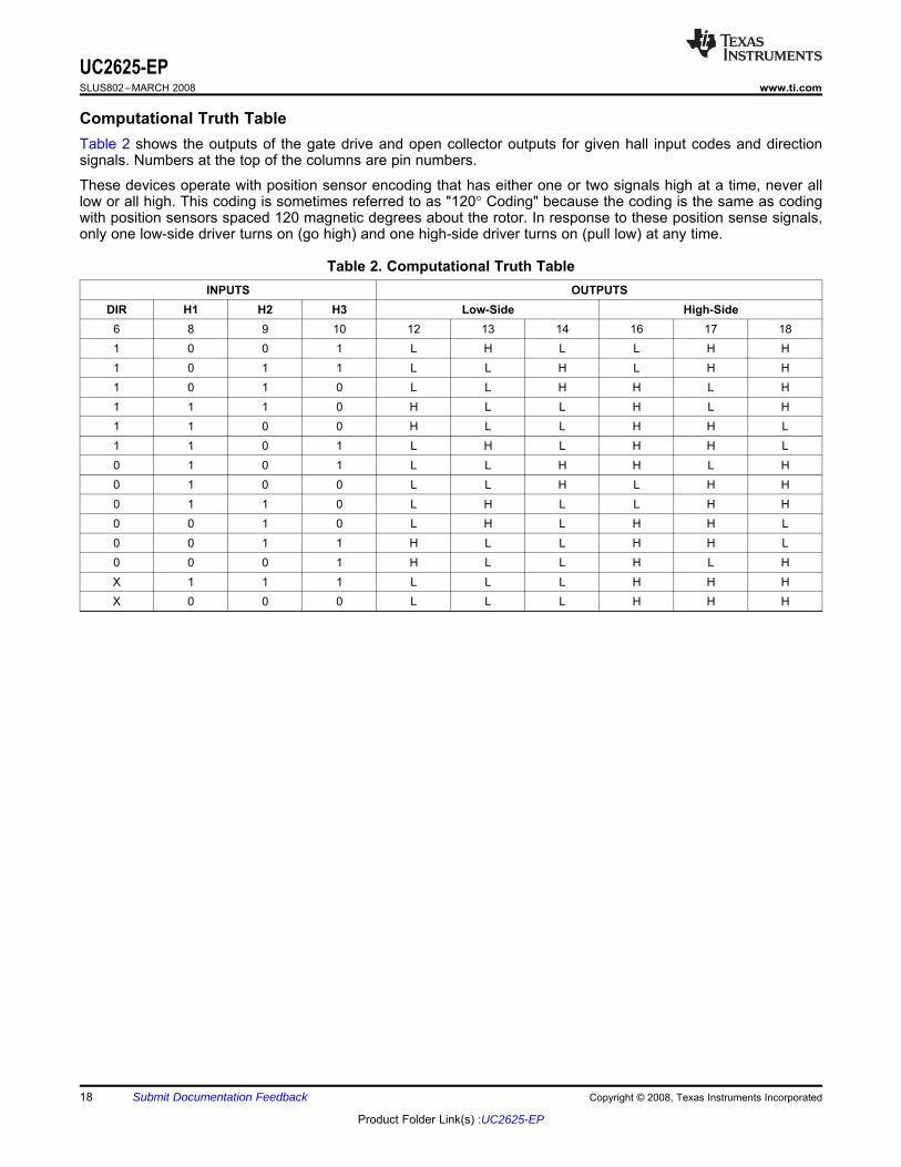
Table 2 shows the outputs of the gate drive and open collector outputs for given hall input codes and directionsignals. Numbers at the top of the columns are pin numbers.These devices operate with position sensor encoding that has either one or two signals high at a time, never alllow or all high. This coding is sometimes referred to as "120° Coding" because the coding is the same as codingwith position sensors spaced 120 magnetic degrees about the rotor. In response to these position sense signals,only one low-side driver turns on (go high) and one high-side driver turns on (pull low) at any time.
Table 2. Computational Truth TableINPUTS OUTPUTS
DIR H1 H2 H3 Low-Side High-Side6 8 9 10 12 13 14 16 17 181 0 0 1 L H L L H H1 0 1 1 L L H L H H1 0 1 0 L L H H L H1 1 1 0 H L L H L H1 1 0 0 H L L H H L1 1 0 1 L H L H H L0 1 0 1 L L H H L H0 1 0 0 L L H L H H0 1 1 0 L H L L H H0 0 1 0 L H L H H L0 0 1 1 H L L H H L0 0 0 1 H L L H L HX 1 1 1 L L L H H HX 0 0 0 L L L H H H
18 Submit Documentation Feedback Copyright © 2008, Texas Instruments Incorporated
Product Folder Link(s) :UC2625-EP
21
27
25
22
6
28
1
15
24326
10kW
3kW10kW
2 19
20
16
11
20mF
100nF
20mF
100nF +
ROSC
33kW
2200pF
COSC
68kW
RT
3nF
CT
BRAKE
5nF
100nF
23 8 9 10 4 5 7
2nF
2nF
2nF
100nF
10kW
5nF240W
240W
17
18
14
13
12
3kW
2N3906
100nF
1k
4kW
TO OTHER
CHANNELS
TO OTHER
CHANNELS
10W
2N3904
10W
IRF9350
IRF532
3kW
FROM
HALL
SENSORS
VMOTOR+15V+5V TO HALL
SENSORSVREF
0.02
W
RS
TO
MOTOR
0.02
W
RD
REQUIRED
FOR
AVERAGE
CURRENT
SENSING
REQUIRED
FOR BRAKE
AND FAST
REVERSE
100mF
+
UC3625
DIR
QUAD
51kW
VREF
UC2625-EPwww.ti.com .................................................................................................................................................................................................. SLUS802–MARCH 2008
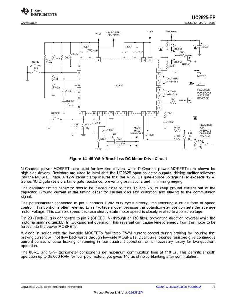
Figure 14. 45-V/8-A Brushless DC Motor Drive Circuit
N-Channel power MOSFETs are used for low-side drivers, while P-Channel power MOSFETs are shown forhigh-side drivers. Resistors are used to level shift the UC2625 open-collector outputs, driving emitter followersinto the MOSFET gate. A 12-V zener clamp insures that the MOSFET gate-source voltage never exceeds 12 V.Series 10-Ω gate resistors tame gate reactance, preventing oscillations and minimizing ringing.The oscillator timing capacitor should be placed close to pins 15 and 25, to keep ground current out of thecapacitor. Ground current in the timing capacitor causes oscillator distortion and slaving to the commutationsignal.The potentiometer connected to pin 1 controls PWM duty cycle directly, implementing a crude form of speedcontrol. This control is often referred to as "voltage mode" because the potentiometer position sets the averagemotor voltage. This controls speed because steady-state motor speed is closely related to applied voltage.Pin 20 (Tach-Out) is connected to pin 7 (SPEED IN) through an RC filter, preventing direction reversal while themotor is spinning quickly. In two-quadrant operation, this reversal can cause kinetic energy from the motor to beforced into the power MOSFETs.A diode in series with the low-side MOSFETs facilitates PWM current control during braking by insuring thatbraking current will not flow backwards through low-side MOSFETs. Dual current-sense resistors give continuouscurrent sense, whether braking or running in four-quadrant operation, an unnecessary luxury for two-quadrantoperation.The 68-kΩ and 3-nF tachometer components set maximum commutation time at 140 µs. This permits smoothoperation up to 35,000 RPM for four-pole motors, yet gives 140 µs of noise blanking after commutation.
Copyright © 2008, Texas Instruments Incorporated Submit Documentation Feedback 19
Product Folder Link(s) :UC2625-EP
PACKAGE OPTION ADDENDUM
www.ti.com 15-Oct-2015
Addendum-Page 1
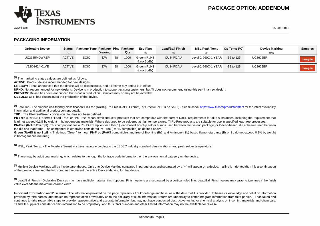
PACKAGING INFORMATION
Orderable Device Status(1)
Package Type PackageDrawing
Pins PackageQty
Eco Plan(2)
Lead/Ball Finish(6)
MSL Peak Temp(3)
Op Temp (°C) Device Marking(4/5)
Samples
UC2625MDWREP ACTIVE SOIC DW 28 1000 Green (RoHS& no Sb/Br)
CU NIPDAU Level-2-260C-1 YEAR -55 to 125 UC2625EP
V62/08624-01YE ACTIVE SOIC DW 28 1000 Green (RoHS& no Sb/Br)
CU NIPDAU Level-2-260C-1 YEAR -55 to 125 UC2625EP
(1) The marketing status values are defined as follows:ACTIVE: Product device recommended for new designs.LIFEBUY: TI has announced that the device will be discontinued, and a lifetime-buy period is in effect.NRND: Not recommended for new designs. Device is in production to support existing customers, but TI does not recommend using this part in a new design.PREVIEW: Device has been announced but is not in production. Samples may or may not be available.OBSOLETE: TI has discontinued the production of the device.
(2) Eco Plan - The planned eco-friendly classification: Pb-Free (RoHS), Pb-Free (RoHS Exempt), or Green (RoHS & no Sb/Br) - please check http://www.ti.com/productcontent for the latest availabilityinformation and additional product content details.TBD: The Pb-Free/Green conversion plan has not been defined.Pb-Free (RoHS): TI's terms "Lead-Free" or "Pb-Free" mean semiconductor products that are compatible with the current RoHS requirements for all 6 substances, including the requirement thatlead not exceed 0.1% by weight in homogeneous materials. Where designed to be soldered at high temperatures, TI Pb-Free products are suitable for use in specified lead-free processes.Pb-Free (RoHS Exempt): This component has a RoHS exemption for either 1) lead-based flip-chip solder bumps used between the die and package, or 2) lead-based die adhesive used betweenthe die and leadframe. The component is otherwise considered Pb-Free (RoHS compatible) as defined above.Green (RoHS & no Sb/Br): TI defines "Green" to mean Pb-Free (RoHS compatible), and free of Bromine (Br) and Antimony (Sb) based flame retardants (Br or Sb do not exceed 0.1% by weightin homogeneous material)
(3) MSL, Peak Temp. - The Moisture Sensitivity Level rating according to the JEDEC industry standard classifications, and peak solder temperature.
(4) There may be additional marking, which relates to the logo, the lot trace code information, or the environmental category on the device.
(5) Multiple Device Markings will be inside parentheses. Only one Device Marking contained in parentheses and separated by a "~" will appear on a device. If a line is indented then it is a continuationof the previous line and the two combined represent the entire Device Marking for that device.
(6) Lead/Ball Finish - Orderable Devices may have multiple material finish options. Finish options are separated by a vertical ruled line. Lead/Ball Finish values may wrap to two lines if the finishvalue exceeds the maximum column width.
Important Information and Disclaimer:The information provided on this page represents TI's knowledge and belief as of the date that it is provided. TI bases its knowledge and belief on informationprovided by third parties, and makes no representation or warranty as to the accuracy of such information. Efforts are underway to better integrate information from third parties. TI has taken andcontinues to take reasonable steps to provide representative and accurate information but may not have conducted destructive testing or chemical analysis on incoming materials and chemicals.TI and TI suppliers consider certain information to be proprietary, and thus CAS numbers and other limited information may not be available for release.
PACKAGE OPTION ADDENDUM
www.ti.com 15-Oct-2015
Addendum-Page 2
In no event shall TI's liability arising out of such information exceed the total purchase price of the TI part(s) at issue in this document sold by TI to Customer on an annual basis.
OTHER QUALIFIED VERSIONS OF UC2625-EP :
• Catalog: UC2625
NOTE: Qualified Version Definitions:
• Catalog - TI's standard catalog product
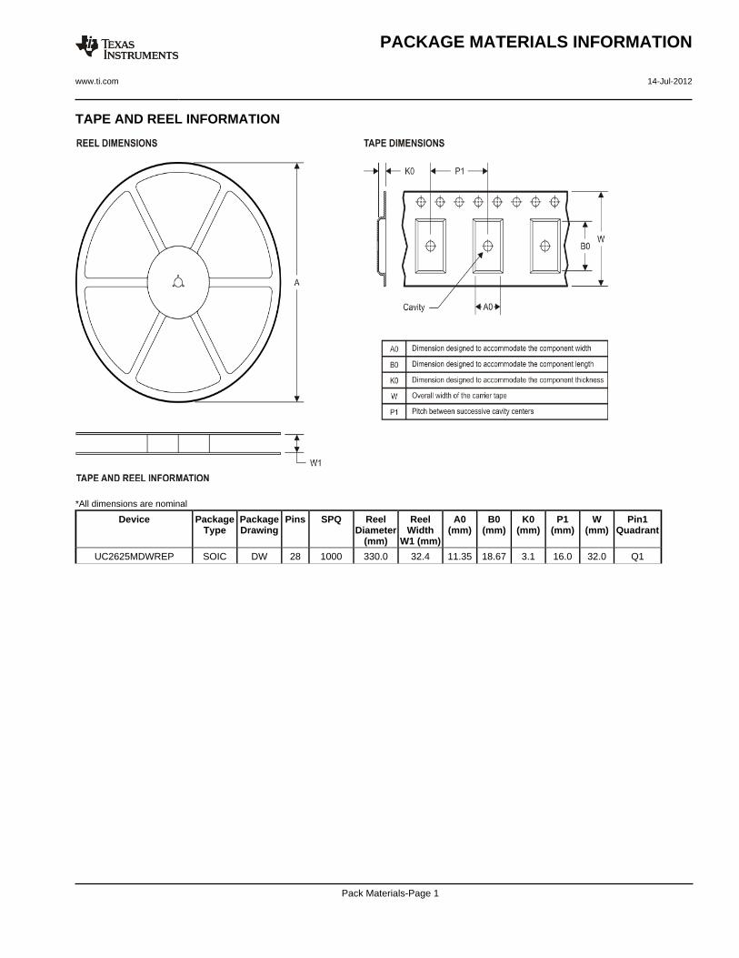
TAPE AND REEL INFORMATION
*All dimensions are nominal
Device PackageType
PackageDrawing
Pins SPQ ReelDiameter
(mm)
ReelWidth
W1 (mm)
A0(mm)
B0(mm)
K0(mm)
P1(mm)
W(mm)
Pin1Quadrant
UC2625MDWREP SOIC DW 28 1000 330.0 32.4 11.35 18.67 3.1 16.0 32.0 Q1
PACKAGE MATERIALS INFORMATION
www.ti.com 14-Jul-2012
Pack Materials-Page 1
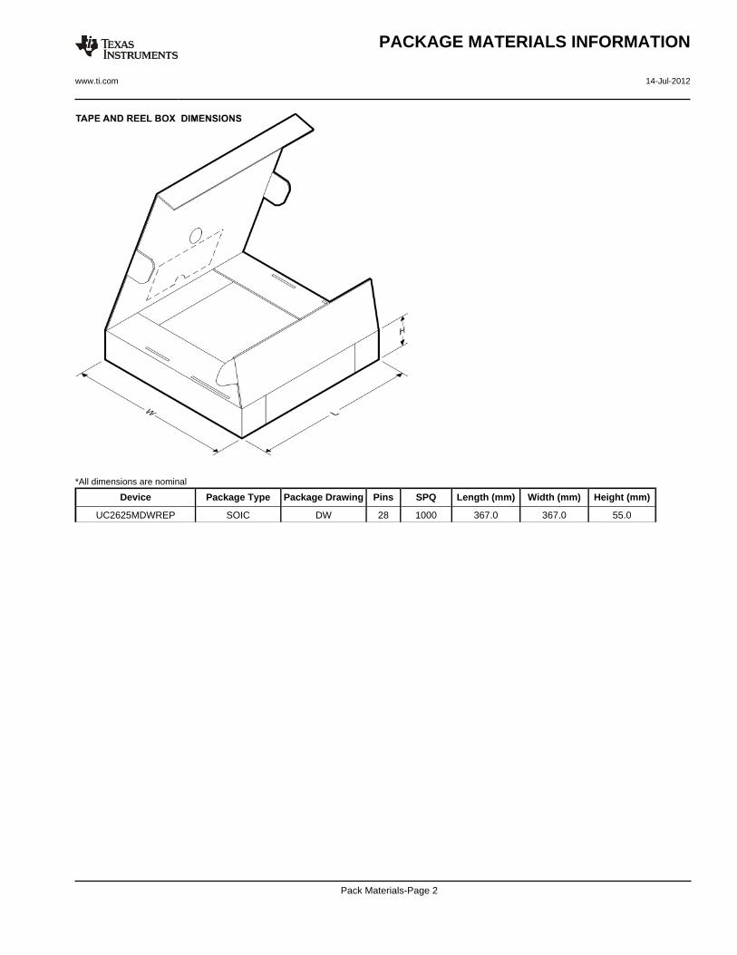
*All dimensions are nominal
Device Package Type Package Drawing Pins SPQ Length (mm) Width (mm) Height (mm)
UC2625MDWREP SOIC DW 28 1000 367.0 367.0 55.0
PACKAGE MATERIALS INFORMATION
www.ti.com 14-Jul-2012
Pack Materials-Page 2
IMPORTANT NOTICE
Texas Instruments Incorporated (TI) reserves the right to make corrections, enhancements, improvements and other changes to itssemiconductor products and services per JESD46, latest issue, and to discontinue any product or service per JESD48, latest issue. Buyersshould obtain the latest relevant information before placing orders and should verify that such information is current and complete.TI’s published terms of sale for semiconductor products (http://www.ti.com/sc/docs/stdterms.htm) apply to the sale of packaged integratedcircuit products that TI has qualified and released to market. Additional terms may apply to the use or sale of other types of TI products andservices.Reproduction of significant portions of TI information in TI data sheets is permissible only if reproduction is without alteration and isaccompanied by all associated warranties, conditions, limitations, and notices. TI is not responsible or liable for such reproduceddocumentation. Information of third parties may be subject to additional restrictions. Resale of TI products or services with statementsdifferent from or beyond the parameters stated by TI for that product or service voids all express and any implied warranties for theassociated TI product or service and is an unfair and deceptive business practice. TI is not responsible or liable for any such statements.Buyers and others who are developing systems that incorporate TI products (collectively, “Designers”) understand and agree that Designersremain responsible for using their independent analysis, evaluation and judgment in designing their applications and that Designers havefull and exclusive responsibility to assure the safety of Designers' applications and compliance of their applications (and of all TI productsused in or for Designers’ applications) with all applicable regulations, laws and other applicable requirements. Designer represents that, withrespect to their applications, Designer has all the necessary expertise to create and implement safeguards that (1) anticipate dangerousconsequences of failures, (2) monitor failures and their consequences, and (3) lessen the likelihood of failures that might cause harm andtake appropriate actions. Designer agrees that prior to using or distributing any applications that include TI products, Designer willthoroughly test such applications and the functionality of such TI products as used in such applications.TI’s provision of technical, application or other design advice, quality characterization, reliability data or other services or information,including, but not limited to, reference designs and materials relating to evaluation modules, (collectively, “TI Resources”) are intended toassist designers who are developing applications that incorporate TI products; by downloading, accessing or using TI Resources in anyway, Designer (individually or, if Designer is acting on behalf of a company, Designer’s company) agrees to use any particular TI Resourcesolely for this purpose and subject to the terms of this Notice.TI’s provision of TI Resources does not expand or otherwise alter TI’s applicable published warranties or warranty disclaimers for TIproducts, and no additional obligations or liabilities arise from TI providing such TI Resources. TI reserves the right to make corrections,enhancements, improvements and other changes to its TI Resources. TI has not conducted any testing other than that specificallydescribed in the published documentation for a particular TI Resource.Designer is authorized to use, copy and modify any individual TI Resource only in connection with the development of applications thatinclude the TI product(s) identified in such TI Resource. NO OTHER LICENSE, EXPRESS OR IMPLIED, BY ESTOPPEL OR OTHERWISETO ANY OTHER TI INTELLECTUAL PROPERTY RIGHT, AND NO LICENSE TO ANY TECHNOLOGY OR INTELLECTUAL PROPERTYRIGHT OF TI OR ANY THIRD PARTY IS GRANTED HEREIN, including but not limited to any patent right, copyright, mask work right, orother intellectual property right relating to any combination, machine, or process in which TI products or services are used. Informationregarding or referencing third-party products or services does not constitute a license to use such products or services, or a warranty orendorsement thereof. Use of TI Resources may require a license from a third party under the patents or other intellectual property of thethird party, or a license from TI under the patents or other intellectual property of TI.TI RESOURCES ARE PROVIDED “AS IS” AND WITH ALL FAULTS. TI DISCLAIMS ALL OTHER WARRANTIES ORREPRESENTATIONS, EXPRESS OR IMPLIED, REGARDING RESOURCES OR USE THEREOF, INCLUDING BUT NOT LIMITED TOACCURACY OR COMPLETENESS, TITLE, ANY EPIDEMIC FAILURE WARRANTY AND ANY IMPLIED WARRANTIES OFMERCHANTABILITY, FITNESS FOR A PARTICULAR PURPOSE, AND NON-INFRINGEMENT OF ANY THIRD PARTY INTELLECTUALPROPERTY RIGHTS. TI SHALL NOT BE LIABLE FOR AND SHALL NOT DEFEND OR INDEMNIFY DESIGNER AGAINST ANY CLAIM,INCLUDING BUT NOT LIMITED TO ANY INFRINGEMENT CLAIM THAT RELATES TO OR IS BASED ON ANY COMBINATION OFPRODUCTS EVEN IF DESCRIBED IN TI RESOURCES OR OTHERWISE. IN NO EVENT SHALL TI BE LIABLE FOR ANY ACTUAL,DIRECT, SPECIAL, COLLATERAL, INDIRECT, PUNITIVE, INCIDENTAL, CONSEQUENTIAL OR EXEMPLARY DAMAGES INCONNECTION WITH OR ARISING OUT OF TI RESOURCES OR USE THEREOF, AND REGARDLESS OF WHETHER TI HAS BEENADVISED OF THE POSSIBILITY OF SUCH DAMAGES.Unless TI has explicitly designated an individual product as meeting the requirements of a particular industry standard (e.g., ISO/TS 16949and ISO 26262), TI is not responsible for any failure to meet such industry standard requirements.Where TI specifically promotes products as facilitating functional safety or as compliant with industry functional safety standards, suchproducts are intended to help enable customers to design and create their own applications that meet applicable functional safety standardsand requirements. Using products in an application does not by itself establish any safety features in the application. Designers mustensure compliance with safety-related requirements and standards applicable to their applications. Designer may not use any TI products inlife-critical medical equipment unless authorized officers of the parties have executed a special contract specifically governing such use.Life-critical medical equipment is medical equipment where failure of such equipment would cause serious bodily injury or death (e.g., lifesupport, pacemakers, defibrillators, heart pumps, neurostimulators, and implantables). Such equipment includes, without limitation, allmedical devices identified by the U.S. Food and Drug Administration as Class III devices and equivalent classifications outside the U.S.TI may expressly designate certain products as completing a particular qualification (e.g., Q100, Military Grade, or Enhanced Product).Designers agree that it has the necessary expertise to select the product with the appropriate qualification designation for their applicationsand that proper product selection is at Designers’ own risk. Designers are solely responsible for compliance with all legal and regulatoryrequirements in connection with such selection.Designer will fully indemnify TI and its representatives against any damages, costs, losses, and/or liabilities arising out of Designer’s non-compliance with the terms and provisions of this Notice.
Mailing Address: Texas Instruments, Post Office Box 655303, Dallas, Texas 75265Copyright © 2018, Texas Instruments Incorporated