Block I Apollo Guidance Computer (AGC) - … · Block I Apollo Guidance Computer (AGC) ... The...
117
Block I Apollo Guidance Computer (AGC) How to build one in your basement Part 7: C++ Simulator John Pultorak December, 2004
Transcript of Block I Apollo Guidance Computer (AGC) - … · Block I Apollo Guidance Computer (AGC) ... The...

Block IApollo Guidance Computer (AGC)
How to build one in your basement
Part 7: C++ Simulator
John Pultorak
December, 2004

Abstract
This report describes my successful project to build a working reproduction of the 1964
prototype for the Block I Apollo Guidance Computer. The AGC is the flight computer for the
Apollo moon landings, and is the world’s first integrated circuit computer.
I built it in my basement. It took me 4 years.
If you like, you can build one too. It will take you less time, and yours will be better than
mine.
I documented my project in 9 separate .pdf files:
Part 1 Overview: Introduces the project.
Part 2 CTL Module: Design and construction of the control module.
Part 3 PROC Module: Design and construction of the processing (CPU) module.
Part 4 MEM Module: Design and construction of the memory module.
Part 5 IO Module: Design and construction of the display/keyboard (DSKY) module.
Part 6 Assembler: A cross-assembler for AGC software development.
Part 7 C++ Simulator: A low-level simulator that runs assembled AGC code.
Part 8 Flight Software: My translation of portions of the COLOSSUS 249 flight
software.
Part 9 Test & Checkout: A suite of test programs in AGC assembly language.
Overview
This document describes my AGC Block I C++ simulator. I developed it almost entirely from
detailed information in this document:
A. Hopkins, R. Alonso, and H. Blair-Smith, "Logical Description for the Apollo Guidance
Computer (AGC4)", R-393, MIT Instrumentation Laboratory, Cambridge, MA, Mar. 1963.
My simulator reproduces not only the AGC instruction set and user-accessible registers, but
all of the registers, all microinstructions, time-pulse generator states, read, write and
memory busses, and control pulses (logic signals) for all AGC subsystems.
The simulator is a tool I used to capture AGC design from the R-393 document. When I got
it working well enough to run my test and checkout software suite (described in part 9) and
flight software (described in part 8), I knew I understood the AGC well enough to build one.
The simulator header and source code files became requirements that guided my AGC logic
design (described in parts 2-5).
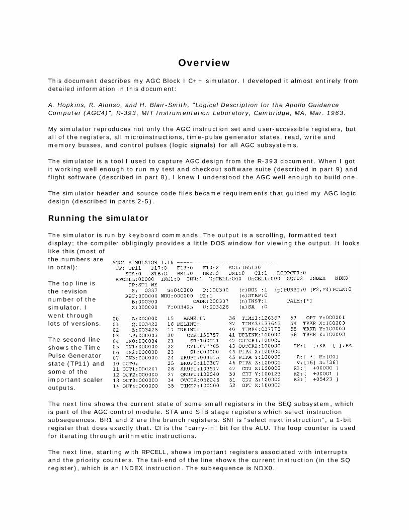
Running the simulator
The simulator is run by keyboard commands. The output is a scrolling, formatted text
display; the compiler obligingly provides a little DOS window for viewing the output. It looks
like this (most of
the numbers are
in octal):
The top line is
the revision
number of the
simulator. I
went through
lots of versions.
The second line
shows the Time
Pulse Generator
state (TP11) and
some of the
important scaler
outputs.
The next line shows the current state of some small registers in the SEQ subsystem, which
is part of the AGC control module. STA and STB stage registers which select instruction
subsequences. BR1 and 2 are the branch registers. SNI is “select next instruction”, a 1-bit
register that does exactly that. CI is the “carry-in” bit for the ALU. The loop counter is used
for iterating through arithmetic instructions.
The next line, starting with RPCELL, shows important registers associated with interrupts
and the priority counters. The tail-end of the line shows the current instruction (in the SQ
register), which is an INDEX instruction. The subsequence is NDX0.

The next line (CP) shows currently asserted control pulses (logic signals). ST1 and WE are
being asserted.
The left side of the next 4 lines shows the state of registers associated with memory (S, G,
P, P2, and CADR), the ALU (B, X, Y, U), and the read bus (RBU) and write bus (WBU).
The right side of those 4 lines shows control inputs for running, stepping, and clocking the
simulator.
The bottom part of the display shows AGC memory. The 2-digit numbers on the left show
memory addresses from 00-56. Each memory location has a name; it’s shown to the right of
the address. Immediately to the right of that is the contents of that location.
Addresses 00-17 are mapped to AGC registers, and are not really part of the AGC eraseable
memory. Addresses 00-03 are the AGC central registers, followed by input and output
registers.
Addresses 16 and 17 are not storage locations, but a means for enabling and disabling
interrupts.
The eraseable memory starts at address 20. Addresses 20-23 are the editing registers.
Writing to these causes the data in the registers to be shifted or rotated.
Addresses 24-27 are used for saving the central registers (00-03) when an interrupt occurs.
Addresses 34-56 are priority counter locations. The AGC will increment or decrement these
based on + pr - logic signals to the priority counter cells.
The lower right of the simulator is the DSKY: the display/keyboard user interface for the
astronauts. The simulator is running the COLOSSUS 249 flight software load, and is
currently executing major mode 0 (P00), verb 16, noun 36, which is a monitor program to
continuously display the command module elapsed time clock. The clock, displayed in R1,
R2, and R3, shows 0 hours, 1 minute, and 54.23 seconds. It updates about once a second
but, of course, you can’t see that here.
Compiler
The simulator was compiled with Microsoft Visual C++ 6.0 Standard Edition.

Commands
Here’s the complete list of commands the simulator knows. The keyboard key you hit is:
{Q}, and the name of the command is: <QUIT>.
Simulator commands{q} <QUIT> Exits the simulator.
{l} <LOAD> The command is a lower case “L”, not a “1". Load fixed
memory with object code produced by the assembler.
The object code files are in Motorola S-Record format
(compatible with EPROM programmers). The command
will ask for a filename.
{m} <MENU> Intended to be a useful menu of simulator command,
but I never got around to it.
Hardware reset commands{p} <POWER UP RESET> Asserts the PURST control signal. This is a power-up
reset signal that is supposed to be automatically
generated when the AGC initially powers on.
{h} <RESET> Asserts the GENRST control signal.
Clock controls{F1} <CLK> Single-step the AGC clock. Only works when MCLK <F2>
has been selected.
{F2} <MCLK> Asserts the MCLK control signal. Disables the free-
running 1MHz clock. When MCLK is selected, you can
single-step the clock by by pressing <F1>.
{F4} <FCLK> Asserts the FCLK control signal. Causes the simulator
clock to free-run at 1MHz. This is the normal operational
mode.

Time pulse generator (TPG) controls{r} <RUN> Toggles between the “run” (1) and “step” (0) modes.
“Run” makes the AGC free-run (the normal mode).
“Step” single-steps the AGC, either by instruction or by
instruction subsequence.
{s} <STEP> Steps the AGC to the next instruction or instruction
sequence when <R> is toggled to the step mode.
{n} <INST> Toggles whether the AGC steps by instruction (1) or
instruction subsequence (0). Each instruction contains
one or more subsequences. Each subsequence is 12
steps or timing pulses long.
Debugger commands{e} <EXAMINE> Examines the contents of memory. The command asks
for a starting address and then displays the memory
data at that address and following locations.
{y} <WATCH> Halts the AGC when any instruction changes a watched
memory location. The command asks for a memory
address (CADR) to watch.
{b} <BREAKPOINT> Toggles a breakpoint on/off. When the breakpoint is on,
it halts the AGC when instruction execution hits that
address.
{d} <DISPLAY> Displays or refreshes the standard AGC register display.
{f} <DEBUG> Displays the currently executing AGC source code. You
can single step with this display and watch the AGC
move through the source code. Very useful for
debugging. A “>” arrow shows the next instruction to be
executed in the listing.
Scaler controls{z} <F17> Manually generates the <F17> scaler pulse. Useful for
testing when the scaler has been toggled to off <C>, or
when you’re single-stepping the AGC.
{x} <F13> Manually generates the <F13> scaler pulse. Useful for
testing when the scaler has been toggled to off <C>, or
when you’re single-stepping the AGC.
{c} <TOGGLE SCALER> Toggle the scaler on/off. When the scaler is off, the F13
and F17 signals are not automatically generated.
Priority counter controls{[} <-CNTR> Manually assert a m inus input to a prority counter cell.
The command will ask for the cell number.
{]} <+CNTR> Manually assert a p lus input to a priority counter cell.
The command will ask for the cell number.
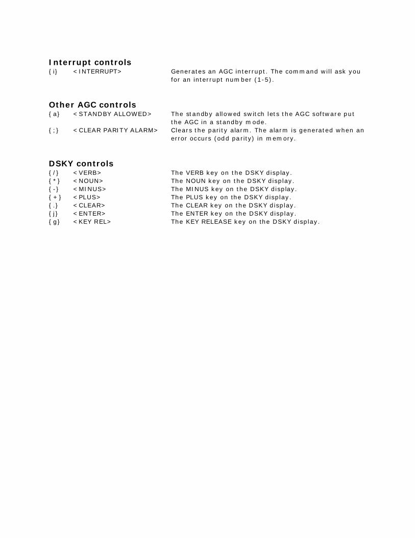
Interrupt controls{i} <INTERRUPT> Generates an AGC interrupt. The command will ask you
for an interrupt number (1-5).
Other AGC controls{a} <STANDBY ALLOWED> The standby allowed switch lets the AGC software put
the AGC in a standby mode.
{;} <CLEAR PARITY ALARM> Clears the parity alarm. The alarm is generated when an
error occurs (odd parity) in memory.
DSKY controls{/} <VERB> The VERB key on the DSKY display.
{*} <NOUN> The NOUN key on the DSKY display.
{-} <MINUS> The MINUS key on the DSKY display.
{+} <PLUS> The PLUS key on the DSKY display.
{.} <CLEAR> The CLEAR key on the DSKY display.
{j} <ENTER> The ENTER key on the DSKY display.
{g} <KEY REL> The KEY RELEASE key on the DSKY display.

Simulator demonstration
Here’s the simulator, demonstrating some COLOSSUS 249 flight software functions. This is
the same scenario I ran in Part 1 using my hardware AGC.
Initialization
At startup, the simulator loads the microinstructions from the EPROM tables. These are the
same tables I eventually used to program the hardware AGC EPROMs.
Reading EPROM: CPM1_8.hex
Reading EPROM: CPM9_16.hex
Reading EPROM: CPM17_24.hex
Reading EPROM: CPM25_32.hex
Reading EPROM: CPM33_40.hex
Reading EPROM: CPM41_48.hex
Reading EPROM: CPM49_56.hex
The simulator is now initialized
and ready for commands.
<LOAD>
The simulator asks, and I enter the name of object files containing the COLOSSUS flight
software.
<POWER UP RESET> <RUN>
<FCLK>
I tell the simulator to start
running, and enable the free-
running clock. The AGC starts
running in real-time with the 1MHz
clock. The DSKY shows major
mode 00 (P00).

Display elapsed time fromthe CM clock
<VERB> <0> <6> <NOUN> <3>
<6> <ENTER>
Test display lights
<VERB> <3> <5> <ENTER>
All DSKY lamps and display
segments illuminate for 5 sec;
after 5 sec, the DSKY lamps
extinguish.
Load component 1 fordataset at octal address50 with octal 123
<VERB> <2> <1> <NOUN> <0>
<1> <ENTER>
Verb/noun display flashes: waiting
for address. Flashing is indicated
by the asterisk to the right of the
NOUN display.

<5> <0> <ENTER>
Verb/noun display flash continues:
waiting for data.
<1> <2> <3> <ENTER>
Octal word from R1 is loaded at
address 50.
Start a monitor programto continuously displayelapsed time from the CMclock
<VERB> <1> <6> <NOUN> <3>
<6> <ENTER>

Display component 1 ofdataset at octal address50
<VERB> <0> <1>
The key rel light flashes because
the CM clock monitor program has
been suspended. This is indicated
by an asterisk in the KR display
above the DSKY.
<NOUN> <0> <1> <ENTER>
Verb/noun display flashes: waiting
for address.
<5> <0> <ENTER>
Octal word from address 50 is
displayed in R1.
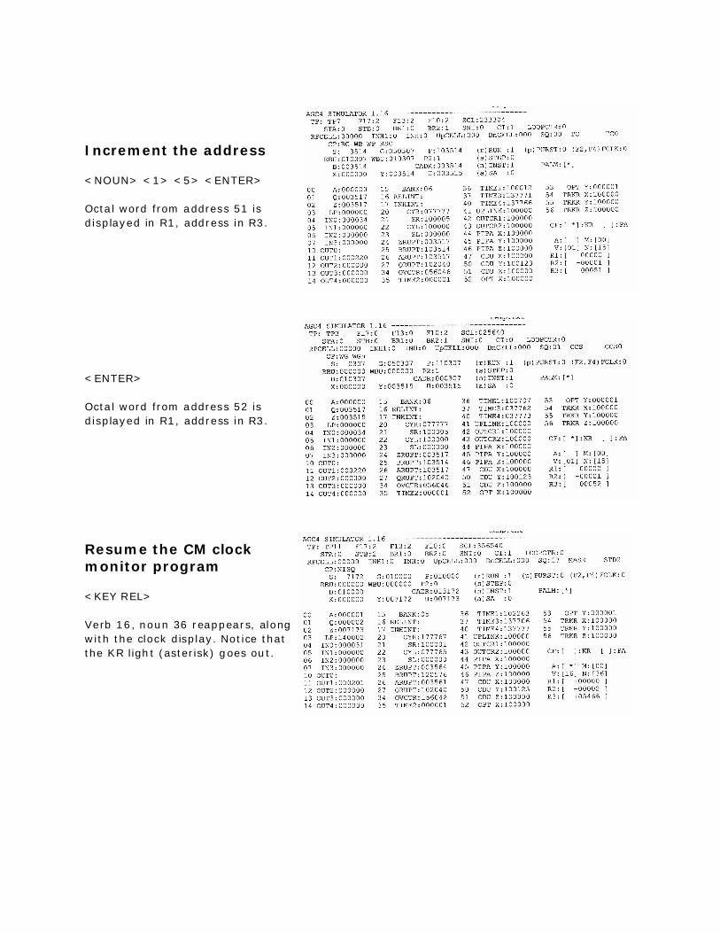
Increment the address
<NOUN> <1> <5> <ENTER>
Octal word from address 51 is
displayed in R1, address in R3.
<ENTER>
Octal word from address 52 is
displayed in R1, address in R3.
Resume the CM clockmonitor program
<KEY REL>
Verb 16, noun 36 reappears, along
with the clock display. Notice that
the KR light (asterisk) goes out.

Terminate the CM clockmonitor program
<VERB> <3> <4> <ENTER>
Change major mode toP00
<VERB> <3> <7> <ENTER>
Verb/noun display flashes:
waiting for major mode.
<0> <0> <ENTER>

The 20-or-so
subsystems in the AGC
are represented by C++
classes. There are some
additional classes for
registers and other
things.
I wanted a simulator
architecture I could
develop quickly that
would easily and directly
map to a hardware logic
design. I went through
16 versions of the
simulator; they’re
discussed at the top of
the AGCMain.cpp file
which contains,
unsurprisingly, the
main().
If you want to run the
simulator, you can
compile it from the
source code given here. To run it, you’ll also need the assembler (discussed in part 6), some
AGC software (parts 8 and 9), and the EPROM tables in Motorola S-Record format. The C++
code to generate these tables is given at the end of part 2.
Here it is, warts and all...

Main (AGCMain.cpp)
/**************************************************************************** * AGC4 (Apollo Guidance Computer) BLOCK I Simulator * * AUTHOR: John Pultorak * DATE: 07/29/02 * FILE: AGCmain.cpp * * VERSIONS: * 1.0 - initial version. * 1.1 - fixed minor bugs; passed automated test and checkout programs: * teco1.asm, teco2.asm, and teco3.asm to test basic instructions, * extended instructions, and editing registers. * 1.2 - decomposed architecture into subsystems; fixed minor bug in DSKY * keyboard logic (not tested in current teco*.asm suite). * Implemented scaler pulses F17, F13, F10. Tied scaler output to * involuntary counters and interrupts. Implemented counter overflow * logic and tied it to interrupts and other counters. Added simple * set/clear breakpoint. Fixed a bug in bank addressing. * 1.3 - fixed bugs in the DSKY. Added 14-bit effective address (CADR) to the * simulator display output. Inhibited interrupts when the operator * single-steps the AGC. * 1.4 - performance enhancements. Recoded the control pulse execution code * for better simulator performance. Also changed the main loop so it * polls the keyboard and system clock less often for better performance. * 1.5 - reversed the addresses of TIME1 and TIME2 so TIME2 occurs first. * This is the way its done in Block II so that a common routine (READLO) * can be used to read the double word for AGC time. * 1.6 - added indicators for 'CHECK FAIL' and 'KEY RELS'. Mapped them to OUT1, * bits 5 and 7. Added a function to display the current location in * the source code list file using the current CADR. * 1.7 - increased length of 'examine' function display. Any changes in DSKY now * force the simulator to update the display immediately. Added a 'watch' * function that looks for changes in a memory location and halts the * AGC. Added the 'UPTL', 'COMP', and "PROG ALM" lights to the DSKY. * 1.8 - started reorganizing the simulator in preparation for H/W logic design. * Eliminated slow (1Hz) clock capability. Removed BUS REQUEST feature. * Eliminated SWRST switch. * 1.9 - eliminated the inclusive 'OR' of the output for all registers onto the * R/W bus. The real AGC OR'ed all register output onto the bus; normally * only one register was enabled at a time, but for some functions several * were simultaneously enabled to take advantage of the 'OR' function (i.e.: * for the MASK instruction). The updated logic will use tristate outputs * to the bus except for the few places where the 'OR' function is actually * needed. Moved the parity bit out of the G register into a 1-bit G15 * register. This was done for convenience because the parity bit in G * is set independently from the rest of the register. * 1.10 - moved the G15 parity register from MBF to the PAR subsystem. Merged SBFWG * and SBEWG pulses into a single SBWG pulse. Deleted the CLG pulse for MBF * (not needed). Separated the ALU read pulses from all others so they can * be executed last to implement the ALU inclusive OR functions. Implemented * separate read and write busses, linked through the ALU. Implemented test * parity (TP) signal in PAR; added parity alarm (PALM) FF to latch PARITY * ALARM indicator in PAR. * 1.11 - consolidated address testing signals and moved them to ADR. Moved memory * read/write functions from MBF to MEM. Merged EMM and FMM subsystems into * MEM. Fixed a bad logic bug in writeMemory() that was causing the load of * the fixed memory to overwrite array boundaries and clobber the CPM table. * Added a memory bus (MEM_DATA_BUS, MEM_PARITY_BUS). * 1.12 - reduced the number of involuntary counters (CTR) from 20 to 8. Eliminated * the SHINC subsequence. Changed the (CTR) sequence and priority registers into * a single synchronization register clocked by WPCTR. Eliminated the fifth * interrupt (UPRUPT; INT). Eliminated (OUT) the signal to read from output * register 0 (the DSKY register), since it was not used and did not provide * any useful function, anyway. Deleted register OUT0 (OUT) which shadowed * the addressed DSKY register and did not provide any useful function. * Eliminated the unused logic that sets the parity bit in OUT2 for downlink * telemetry. * 1.13 - reorganized the CPM control pulses into CPM-A, CPM-B, and CPM-C groups. * Added the SDV1, SMP1, and SRSM3 control pulses to CPM-A to indicate when * those subsequences are active; these signals are input to CPM-C. Moved the * ISD function into CPM-A. Fixed a minor bug causing subsequence RSM3 to be * displayed as RSM0. Added GENRST to clear most registers during STBY. * 1.14 - Moved CLISQ to TP1 to fix a problem in the hardware AGC. CLISQ was clearing

* SNI on CLK2 at TP12, but the TPG was advancing on CLK1 which occurs after * CLK2, so the TPG state machine was not seeing SNI and was not moving to * the correct state. In this software simulation, everything advances on * the same pulse, so it wasn't a problem to clear SNI on TP12. Added a * switch to enable/disable the scaler. * 1.15 - Reenabled interrupts during stepping (by removing MON::RUN) signals from * CPM-A and CPM-C logic). Interrupts can be prevented by disabling the scaler. * Fixed a problem with INHINT1; it is supposed to prevent an interrupt * between instructions if there's an overflow. It was supposed to be cleared * on TP12 after SNI (after a new instruction), but was being cleared on TP12 * after every subsequence. * 1.16 - Changed CPM-A to load and use EPROM tables for the control pulse matrix. The * EPROM tables are negative logic (0=asserted), but this simulator expects * positive logic, so each word is bit-flipped when the EPROM tables load * during simulator initialization. * SOURCES: * Mostly based on information from "Logical Description for the Apollo Guidance * Computer (AGC4)", Albert Hopkins, Ramon Alonso, and Hugh Blair-Smith, R-393, * MIT Instrumentation Laboratory, 1963. * * PORTABILITY: * Compiled with Microsoft Visual C++ 6.0 standard edition. Should be fairly * portable, except for some Microsoft-specific I/O and timer calls in this file. * * NOTE: set tabs to 4 spaces to keep columns formatted correctly. * ***************************************************************************** */
#include <conio.h>
#include <iostream.h>#include <stdio.h>#include <stdlib.h>#include <string.h>#include <conio.h>#include <stdio.h>#include <time.h>#include <ctype.h>
#include "reg.h"
#include "TPG.h"#include "MON.h"#include "SCL.h"#include "SEQ.h"#include "INP.h"#include "OUT.h"#include "BUS.h"#include "DSP.h"#include "ADR.h"#include "PAR.h"#include "MBF.h"#include "MEM.h"#include "CTR.h"#include "INT.h"#include "KBD.h"#include "CRG.h"#include "ALU.h"#include "CPM.h"#include "ISD.h"#include "CLK.h"
extern bool dskyChanged;
//-----------------------------------------------------------------------// CONTROL LOGIC
void genAGCStates(){
// 1) Decode the current instruction subsequence (glbl_subseq).// SEQ::glbl_subseq = CPM::instructionSubsequenceDecoder();
// 2) Build a list of control pulses for this state.CPM::controlPulseMatrix();

// 3) Execute the control pulses for this state. In the real AGC, these occur// simultaneously. Since we can't achieve that here, we break it down into the// following steps:// Most operations involve data transfers--usually reading data from// a register onto a bus and then writing that data into another register. To// approximate this, we first iterate through all registers to perform// the 'read' operation--this transfers data from register to bus.// Then we again iterate through the registers to do 'write' operations,// which move data from the bus back into the register.
BUS::glbl_READ_BUS = 0; // clear bus; necessary because words are logical // OR'ed onto the bus.
MEM::MEM_DATA_BUS = 0; // clear data lines: memory bits 15-1MEM::MEM_PARITY_BUS = 0; // parity line: memory bit 16
// Now start executing the pulses:
// First, read register outputs onto the bus or anywhere else.int i;for(i=0; i<MAXPULSES && SEQ::glbl_cp[i] != NO_PULSE; i++){
CLK::doexecR(SEQ::glbl_cp[i]);}
// Next, execute ALU read pulses. See comments in ALU .C fileALU::glbl_BUS = 0;for(i=0; i<MAXPULSES && SEQ::glbl_cp[i] != NO_PULSE; i++){
CLK::doexecR_ALU(SEQ::glbl_cp[i]);}BUS::glbl_WRITE_BUS = BUS::glbl_READ_BUS; // in case nothing is logically OR'ed below;for(i=0; i<MAXPULSES && SEQ::glbl_cp[i] != NO_PULSE; i++){
CLK::doexecR_ALU_OR(SEQ::glbl_cp[i]);}
// Now, write the bus and any other signals into the register inputs.
for(i=0; i<MAXPULSES && SEQ::glbl_cp[i] != NO_PULSE; i++){
CLK::doexecW(SEQ::glbl_cp[i]);}
// Always execute these pulses.SCL::doexecWP_SCL();SCL::doexecWP_F17();SCL::doexecWP_F13();SCL::doexecWP_F10();TPG::doexecWP_TPG();
}
//-----------------------------------------------------------------------// SIMULATION LOGIC
// contains prefix for source filename; i.e.: the portion// of the filename before .obj or .lst
char filename[80];
char* getCommand(char* prompt){
static char s[80];char* sp = s;
cout << prompt; cout.flush();
char key;while((key = _getch()) != 13){
if(isprint(key)){
cout << key; cout.flush();*sp = key; sp++;
}
else if(key == 8 && sp != s){
cout << key << " " << key; cout.flush();sp--;
}}*sp = '\0';return s;
}
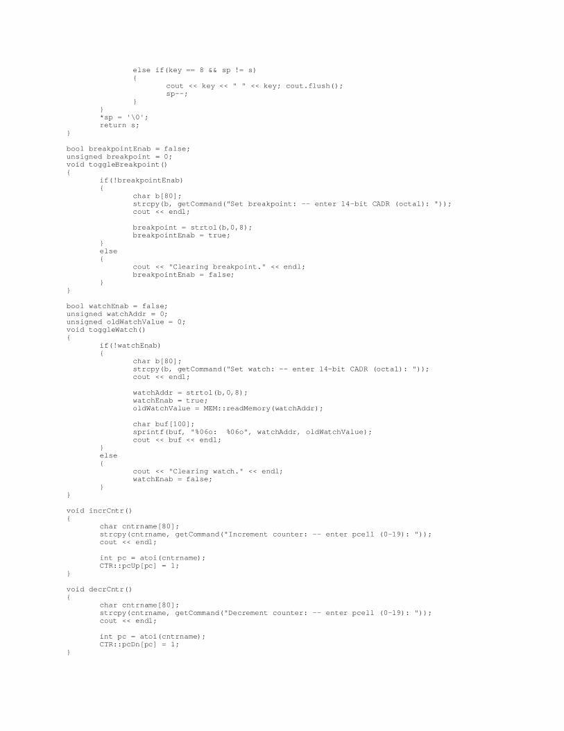
bool breakpointEnab = false;unsigned breakpoint = 0;void toggleBreakpoint(){
if(!breakpointEnab){
char b[80];strcpy(b, getCommand("Set breakpoint: -- enter 14-bit CADR (octal): "));cout << endl;
breakpoint = strtol(b,0,8);breakpointEnab = true;
}else{
cout << "Clearing breakpoint." << endl;breakpointEnab = false;
}}
bool watchEnab = false;unsigned watchAddr = 0;unsigned oldWatchValue = 0;void toggleWatch(){
if(!watchEnab){
char b[80];strcpy(b, getCommand("Set watch: -- enter 14-bit CADR (octal): "));cout << endl;
watchAddr = strtol(b,0,8);watchEnab = true;oldWatchValue = MEM::readMemory(watchAddr);
char buf[100];sprintf(buf, "%06o: %06o", watchAddr, oldWatchValue);cout << buf << endl;
}else{
cout << "Clearing watch." << endl;watchEnab = false;
}}
void incrCntr(){
char cntrname[80];strcpy(cntrname, getCommand("Increment counter: -- enter pcell (0-19): "));cout << endl;
int pc = atoi(cntrname);CTR::pcUp[pc] = 1;
}
void decrCntr(){
char cntrname[80];strcpy(cntrname, getCommand("Decrement counter: -- enter pcell (0-19): "));cout << endl;
int pc = atoi(cntrname);CTR::pcDn[pc] = 1;
}
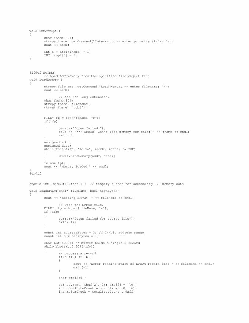
void interrupt(){
char iname[80];strcpy(iname, getCommand("Interrupt: -- enter priority (1-5): "));cout << endl;
int i = atoi(iname) - 1;INT::rupt[i] = 1;
}
#ifdef NOTDEF// Load AGC memory from the specified file object file
void loadMemory(){
strcpy(filename, getCommand("Load Memory -- enter filename: "));cout << endl;
// Add the .obj extension.char fname[80];strcpy(fname, filename);strcat(fname, ".obj");
FILE* fp = fopen(fname, "r");if(!fp){
perror("fopen failed:");cout << "*** ERROR: Can't load memory for file: " << fname << endl;return;
}unsigned addr;unsigned data;while(fscanf(fp, "%o %o", &addr, &data) != EOF){
MEM::writeMemory(addr, data);}fclose(fp);cout << "Memory loaded." << endl;
}#endif
static int loadBuf[0xffff+1]; // tempory buffer for assembling H,L memory data
void loadEPROM(char* fileName, bool highBytes){
cout << "Reading EPROM: " << fileName << endl;
// Open the EPROM file.FILE* ifp = fopen(fileName, "r");if(!ifp){
perror("fopen failed for source file");exit(-1);
}
const int addressBytes = 3; // 24-bit address rangeconst int sumCheckBytes = 1;
char buf[4096]; // buffer holds a single S-Recordwhile(fgets(buf,4096,ifp)){
// process a recordif(buf[0] != 'S'){
cout << "Error reading start of EPROM record for: " << fileName << endl;exit(-1);
}
char tmp[256];
strncpy(tmp, &buf[2], 2); tmp[2] = '\0';int totalByteCount = strtol(tmp, 0, 16);int mySumCheck = totalByteCount & 0xff;

strncpy(tmp, &buf[4], 6); tmp[addressBytes*2] = '\0';int address = strtol(tmp, 0, 16);mySumCheck = (mySumCheck + ((address & 0xff0000) >> 16)) % 256;mySumCheck = (mySumCheck + ((address & 0x00ff00) >> 8)) % 256;mySumCheck = (mySumCheck + ((address & 0x0000ff) )) % 256;
//cout << hex << totalByteCount << ", " << address << dec << endl;
int dataBytes = totalByteCount - addressBytes - sumCheckBytes;
int i = (addressBytes+2)*2; // index to 1st databyte char.for(int j=0; j<dataBytes; j++){
// get a data bytestrncpy(tmp, &buf[i], 2); tmp[2] = '\0';int data = strtol(tmp, 0, 16);//cout << hex << data << dec << endl;mySumCheck = (mySumCheck + data) % 256;
if(highBytes){
loadBuf[address] = loadBuf[address] | ((data << 8) & 0xff00);}else{
loadBuf[address] = loadBuf[address] | (data & 0xff);}address++;
i+=2; // bump to next databyte char}strncpy(tmp, &buf[i], 2); tmp[2] = '\0';int sumCheck = strtol(tmp, 0, 16);
if(sumCheck != ((~mySumCheck) & 0xff)){
cout << "sumCheck failed; file: " << fileName << ", address: " << hex << address << ", sumCheck: " << sumCheck << ", mySumCheck: " << mySumCheck << dec << endl;
exit(-1);}
}fclose(ifp);cout << "Memory loaded." << endl;
}
// Load AGC memory from the specified EPROM filesvoid loadMemory(){
strcpy(filename, getCommand("Load Memory -- enter filename: "));cout << endl;
char fname[80];
// Add the _H.hex extension.strcpy(fname, filename);strcat(fname, "_H.hex");
loadEPROM(fname, true);
// Add the _L.hex extension.strcpy(fname, filename);strcat(fname, "_L.hex");
loadEPROM(fname, false);
//*******************************************************************// EPROM is now in loadBuf; move it to AGC memory.// AGC fixed memory only uses NUMFBANK banks.
for(int address=1024; address < 1024*(NUMFBANK+1); address++){
// Don't load address region 0-1023; that region is allocated

// to eraseable memory.//cout << "loading CADR=" << hex << address << endl;MEM::writeMemory(address, loadBuf[address]);
}//*******************************************************************
}
// Write the entire contents of fixed and// eraseable memory to the specified file.// Does not write the registers
void saveMemory(char* filename){
FILE* fp = fopen(filename, "w");if(!fp){
perror("*** ERROR: fopen failed:");exit(-1);
}char buf[100];for(unsigned addr=020; addr<=031777; addr++){
sprintf(buf, "%06o %06o\n", addr, MEM::readMemory(addr));fputs(buf, fp);
}fclose(fp);
}
void examineMemory(){
char theAddress[20];strcpy(theAddress, getCommand("Examine Memory -- enter address (octal): "));cout << endl;
unsigned address = strtol(theAddress, 0, 8);
char buf[100];for(unsigned i=address; i<address+23; i++){
sprintf(buf, "%06o: %06o", i, MEM::readMemory(i));cout << buf << endl;
}}
// Returns true if time (s) elapsed since last time it returned true; does not block// search for "Time Management"
bool checkElapsedTime(time_t s){
if(!s) return true;
static clock_t start = clock();clock_t finish = clock();
double duration = (double)(finish - start) / CLOCKS_PER_SEC;if(duration >= s){ start = finish;
return true;}return false;
}
// Blocks until time (s) has elapsed.void delay(time_t s){
if(!s) return;
clock_t start = clock();clock_t finish = 0;double duration = 0;
do{
finish = clock();}while((duration = (double)(finish - start) / CLOCKS_PER_SEC) < s);

}
void updateAGCDisplay(){
static bool displayTimeout = false;static int clockCounter = 0;
if(checkElapsedTime(2)) displayTimeout = true;if(MON::FCLK){
if(MON::RUN){
// update every 2 seconds at the start of a new instructionif(displayTimeout || dskyChanged){
clockCounter++;if(
(TPG::register_SG.read() == TP12 && SEQ::register_SNI.read() == 1) ||
(TPG::register_SG.read() == STBY) ||clockCounter > 500 ||dskyChanged)
{MON::displayAGC();displayTimeout = false;clockCounter = 0;dskyChanged = false;
}}
}else{
static bool displayOnce = false;if(TPG::register_SG.read() == WAIT){
if(displayOnce == false){
MON::displayAGC();displayOnce = true;clockCounter = 0;
}}else{
displayOnce = false;}
}}else
MON::displayAGC(); // When the clock is manual or slow, always update.}
void showMenu(){
cout << "AGC4 EMULATOR MENU:" << endl;cout << " 'r' = RUN: toggle RUN/HALT switch upward to the RUN position." << endl;
}
const int startCol = 0; // columns are numbered 0-nconst int colLen = 5; // number of chars in column
const int maxLines = 23; // # of total lines to displayconst int noffset = 10; // # of lines prior to, and including, selected line
const int maxLineLen = 79;
void showSourceCode(){
// Add the .lst extension.char fname[80];strcpy(fname, filename);strcat(fname, ".lst");
// Open the file containing the source code listing.FILE* fp = fopen(fname, "r");if(!fp)

{perror("fopen failed:");cout << "*** ERROR: Can't load source list file: " << fname << endl;return;
}cout << endl;
// Get the address of the source code line to display.// The address we want is the current effective address is the// S and bank registers.
char CADR[colLen+1];sprintf(CADR, "%05o", ADR::getEffectiveAddress());
int op = 0; // offset indexlong foffset[noffset];for(int i=0; i<noffset; i++) foffset[i]=0;
bool foundit = false;int lineCount = 0;
char s[256];char valString[20];char out[256];
while(!feof(fp)){
if(!foundit){
foffset[op] = ftell(fp);op = (op + 1) % noffset;
}
// Read a line of the source code list file.if(fgets(s, 256, fp)){
// Get the address (CADR) from the line.strncpy(valString, s+startCol, colLen);valString[colLen]='\0';
// 'foundit' is true after we have found the desired line.if(foundit){
if(strcmp(valString,CADR) == 0)cout << ">";
elsecout << " ";
// truncate line so it fits in 80 col displaystrncpy(out, s, maxLineLen);out[maxLineLen] = '\0';cout << out;
lineCount++;if(lineCount >= maxLines)
break;}else{
if(strcmp(valString, CADR) == 0){
// Reposition the file pointer back several lines so// we can see the code that preceeds the desired// line, too.
foundit = true;fseek(fp, foffset[op], 0);
}}
}}fclose(fp);
}
void main(int argc, char* argv[]){

CPM::readEPROM( "CPM1_8.hex", CPM::EPROM1_8);CPM::readEPROM( "CPM9_16.hex", CPM::EPROM9_16);CPM::readEPROM("CPM17_24.hex", CPM::EPROM17_24);CPM::readEPROM("CPM25_32.hex", CPM::EPROM25_32);CPM::readEPROM("CPM33_40.hex", CPM::EPROM33_40);CPM::readEPROM("CPM41_48.hex", CPM::EPROM41_48);CPM::readEPROM("CPM49_56.hex", CPM::EPROM49_56);
bool singleClock = false;
genAGCStates();MON::displayAGC();
while(1){
// NOTE: assumes that the display is always pointing to the start of// a new line at the top of this loop!
// Clock the AGC, but between clocks, poll the keyboard// for front-panel input by the user. This uses a Microsoft function;// substitute some other non-blocking function to access the keyboard// if you're porting this to a different platform.cout << "> "; cout.flush(); // display prompt
while( !_kbhit() ){
if(MON::FCLK || singleClock){
// This is a performance enhancement. If the AGC is running,// don't check the keyboard or simulator display every// simulation cycle, because that slows the simulator // down too much.
int genStateCntr = 100;do { CLK::clkAGC();
singleClock = false;
genAGCStates(); genStateCntr--;
// Needs more work. It doesn't always stop at the// right location and sometimes stops at the// instruction afterwards, too.
if(breakpointEnab && breakpoint == ADR::getEffectiveAddress())
{MON::RUN = 0;
}
// Halt right after instr that changes a watched// memory location.
if(watchEnab){
unsigned newWatchValue = MEM::readMemory(watchAddr);if(newWatchValue != oldWatchValue){
MON::RUN = 0;}oldWatchValue = newWatchValue;
}
} while (MON::FCLK && MON::RUN && genStateCntr > 0);
updateAGCDisplay();
}// for convenience, clear the single step switch on TP1; in the// hardware AGC, this happens when the switch is releasedif(MON::STEP && TPG::register_SG.read() == TP1) MON::STEP = 0;
}char key = _getch();
// Keyboard controls for front-panel:switch(key)

{// AGC controls// simulator controls
case 'q': cout << "QUIT..." << endl; exit(0);case 'm': showMenu(); break;
case 'd': genAGCStates(); MON::displayAGC(); break; // update display
case 'l': loadMemory(); break;case 'e': examineMemory(); break;
case 'f':showSourceCode();break;
case ']': incrCntr(); //genAGCStates();//displayAGC(EVERY_CYCLE);break;
case '[': decrCntr(); //genAGCStates();//displayAGC(EVERY_CYCLE);break;
case 'i': interrupt(); //genAGCStates();//displayAGC(EVERY_CYCLE);break;
case 'z'://SCL::F17 = (SCL::F17 + 1) % 2; genAGCStates();MON::displayAGC();break;
case 'x'://SCL::F13 = (SCL::F13 + 1) % 2; genAGCStates();MON::displayAGC();break;
case 'c': MON::SCL_ENAB = (MON::SCL_ENAB + 1) % 2;genAGCStates();MON::displayAGC();break;
case 'r': MON::RUN = (MON::RUN + 1) % 2; genAGCStates();if(!MON::FCLK) MON::displayAGC();break;
case 's': MON::STEP = (MON::STEP + 1) % 2; genAGCStates();if(!MON::FCLK) MON::displayAGC();break;
case 'a': MON::SA = (MON::SA + 1) % 2; genAGCStates();MON::displayAGC();break;
case 'n': MON::INST = (MON::INST + 1) % 2; genAGCStates();

MON::displayAGC();break;
case 'p': MON::PURST = (MON::PURST + 1) % 2;genAGCStates();MON::displayAGC();break;
case 'b':toggleBreakpoint();break;
case 'y':toggleWatch();break;
case ';': // Clear ALARM indicators
PAR::CLR_PALM(); // Asynchronously clear PARITY FAILMON::displayAGC();break;
// DSKY:case '0': KBD::keypress(KEYIN_0); break;case '1': KBD::keypress(KEYIN_1); break;case '2': KBD::keypress(KEYIN_2); break;case '3': KBD::keypress(KEYIN_3); break;case '4': KBD::keypress(KEYIN_4); break;case '5': KBD::keypress(KEYIN_5); break;case '6': KBD::keypress(KEYIN_6); break;case '7': KBD::keypress(KEYIN_7); break;case '8': KBD::keypress(KEYIN_8); break;case '9': KBD::keypress(KEYIN_9); break;case '+': KBD::keypress(KEYIN_PLUS); break;case '-': KBD::keypress(KEYIN_MINUS); break;case '.': KBD::keypress(KEYIN_CLEAR); break;case '/': KBD::keypress(KEYIN_VERB); break;case '*': KBD::keypress(KEYIN_NOUN); break;case 'g': KBD::keypress(KEYIN_KEY_RELEASE); break;case 'h': KBD::keypress(KEYIN_ERROR_RESET); break;case 'j': KBD::keypress(KEYIN_ENTER); break;
case '\0': // must be a function keykey = _getch();switch(key){case 0x3b: // F1: single clock pulse (when system clock off)
singleClock = true; break; case 0x3c: // F2: manual clock (FCLK=0)
MON::FCLK = 0; genAGCStates(); MON::displayAGC(); break; case 0x3e: // F4: fast clock (FCLK=1)
MON::FCLK = 1; genAGCStates(); MON::displayAGC(); break;default: cout << "function key: " << key << "="
<< hex << (int) key << dec << endl;}break;
//default: cout << "??" << endl;default: cout << key << "=" << hex << (int) key << dec << endl;}
}}

ADR (ADR.h)
/**************************************************************************** * ADR - MEMORY ADDRESS subsystem * * AUTHOR: John Pultorak * DATE: 9/22/01 * FILE: ADR.h * * VERSIONS: * * DESCRIPTION: * Memory address for the Block 1 Apollo Guidance Computer prototype (AGC4). * * SOURCES: * Mostly based on information from "Logical Description for the Apollo * Guidance Computer (AGC4)", Albert Hopkins, Ramon Alonso, and Hugh * Blair-Smith, R-393, MIT Instrumentation Laboratory, 1963. * * NOTES: * ***************************************************************************** */#ifndef ADR_H#define ADR_H
enum specialRegister { // octal addresses of special registers// Flip-Flop registers
A_ADDR =00,Q_ADDR =01,Z_ADDR =02,LP_ADDR =03,IN0_ADDR =04,IN1_ADDR =05,IN2_ADDR =06,IN3_ADDR =07,OUT0_ADDR =010,OUT1_ADDR =011,OUT2_ADDR =012,OUT3_ADDR =013,OUT4_ADDR =014,BANK_ADDR =015,
// No bits in these registersRELINT_ADDR =016,INHINT_ADDR =017,
// In eraseable memoryCYR_ADDR =020,SR_ADDR =021,CYL_ADDR =022,SL_ADDR =023,ZRUPT_ADDR =024,BRUPT_ADDR =025,ARUPT_ADDR =026,QRUPT_ADDR =027,
};
class regS : public reg { public:
regS() : reg(12, "%04o") { }};
class regBNK : public reg { public:
regBNK() : reg(4, "%02o") { }};
class ADR
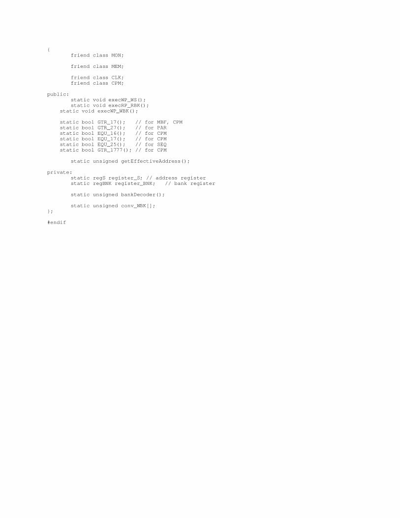
{friend class MON;
friend class MEM;
friend class CLK;friend class CPM;
public:static void execWP_WS();static void execRP_RBK();
static void execWP_WBK();
static bool GTR_17(); // for MBF, CPM static bool GTR_27(); // for PAR static bool EQU_16(); // for CPM static bool EQU_17(); // for CPM static bool EQU_25(); // for SEQ static bool GTR_1777(); // for CPM
static unsigned getEffectiveAddress();
private:static regS register_S; // address registerstatic regBNK register_BNK; // bank register
static unsigned bankDecoder();
static unsigned conv_WBK[];};
#endif

ADR (ADR.cpp)
/**************************************************************************** * ADR - MEMORY ADDRESS subsystem * * AUTHOR: John Pultorak * DATE: 9/22/01 * FILE: ADR.cpp * * NOTES: see header file. * ***************************************************************************** */#include "reg.h"#include "ADR.h"#include "SEQ.h"#include "BUS.h"
regS ADR::register_S; // address registerregBNK ADR::register_BNK; // bank register
// transfer bits 14-11 from the bus into the 4-bit bank registerunsigned ADR::conv_WBK[] ={ BX, BX, BX, BX, BX, BX, BX, BX, BX, BX, BX, BX, B14, B13, B12, B11 };
void ADR::execWP_WS(){
register_S.write(BUS::glbl_WRITE_BUS);}
void ADR::execRP_RBK(){
BUS::glbl_READ_BUS = register_BNK.read() << 10;}
void ADR::execWP_WBK(){
register_BNK.writeShift(BUS::glbl_WRITE_BUS, ADR::conv_WBK);}
bool ADR::GTR_27(){
return (register_S.read() > 027); }
bool ADR::GTR_17(){
// check: address is not a central registerreturn (register_S.read() > 017);
}
bool ADR::EQU_25(){
return (register_S.read() == 025); }
bool ADR::EQU_17(){
// check: instruction is INHINT (INDEX 017)return (register_S.read() == 017);
}
bool ADR::EQU_16(){
// check: instruction is RELINT (INDEX 016))return (register_S.read() == 016);
}
bool ADR::GTR_1777(){
// check: address is fixed memory

return (register_S.read() > 01777); }
unsigned ADR::bankDecoder(){
// Memory is organized into 13 banks of 1K words each. The banks are numbered// 0-12. Bank 0 is erasable memory; banks 1-12 are fixed (rope) memory. The 10// lower bits in the S register address memory inside a bank. The 2 upper bits// in the S register select the bank. If the 2 upper bits are both 1, the 4-bit// bank register is used to select the bank.// 12 11 Bank// 0 0 0 erasable memory// 0 1 1 fixed-fixed 1 memory// 1 0 2 fixed-fixed 2 memory// 1 1 3-12 fixed-switchable memory (bank register selects bank)unsigned bank = ADR::register_S.readField(12,11);if(bank == 3){
// fixed-switchableif(register_BNK.read() <= 03) // defaults to 6000 - 7777
return 03;else
return register_BNK.read(); // 10000 - 31777}else
return bank; // erasable or fixed-fixed}
unsigned ADR::getEffectiveAddress(){
// Return the 14-bit address selected by lower 10 bits of the S register (1K)// and the bank decoder (which selects the 1K bank)
unsigned lowAddress = ADR::register_S.readField(10,1);
if(ADR::bankDecoder() == 0)return lowAddress;
unsigned highAddress = ADR::bankDecoder() << 10;return highAddress | lowAddress;
}
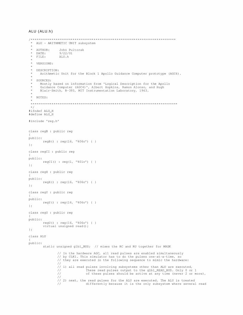
ALU (ALU.h)
/**************************************************************************** * ALU - ARITHMETIC UNIT subsystem * * AUTHOR: John Pultorak * DATE: 9/22/01 * FILE: ALU.h * * VERSIONS: * * DESCRIPTION: * Arithmetic Unit for the Block 1 Apollo Guidance Computer prototype (AGC4). * * SOURCES: * Mostly based on information from "Logical Description for the Apollo * Guidance Computer (AGC4)", Albert Hopkins, Ramon Alonso, and Hugh * Blair-Smith, R-393, MIT Instrumentation Laboratory, 1963. * * NOTES: * ***************************************************************************** */#ifndef ALU_H#define ALU_H
#include "reg.h"
class regB : public reg { public:
regB() : reg(16, "%06o") { }};
class regCI : public reg { public:
regCI() : reg(1, "%01o") { }};
class regX : public reg { public:
regX() : reg(16, "%06o") { }};
class regY : public reg { public:
regY() : reg(16, "%06o") { }};
class regU : public reg { public:
regU() : reg(16, "%06o") { }virtual unsigned read();
};
class ALU{public:
static unsigned glbl_BUS; // mixes the RC and RU together for MASK
// In the hardware AGC, all read pulses are enabled simultaneously// by CLK1. This simulator has to do the pulses one-at-a-time, so// they are executed in the following sequence to mimic the hardware://// 1) all read pulses involving subsystems other than ALU are executed,// These read pulses output to the glbl_READ_BUS. Only 0 or 1// of these pulses should be active at any time (never 2 or more),//// 2) next, the read pulses for the ALU are executed. The ALU is treated// differently because it is the only subsystem where several read

// pulses can be active simultaneously. In the original AGC, these// pulses 'inclusive OR' their output to the glbl_READ_BUS, so the// simulator has be implemented to execute all read pulses other than// the ALU reads first, so the ALU will have the bus data it needs// in order to do the inclusive OR.// In the recreated AGC hardware design, the ALU is also the subsystem// that links the glbl_READ_BUS to the glbl_WRITE_BUS.//// The recreated ALU hardware design checks whether anything is being// written to the glbl_READ_BUS by the other subsystems. If not, it// outputs zeroes to the glbl_READ_BUS for input to the inclusive OR// operation.// It then transfers data on the glbl_READ_BUS to the glbl_WRITE_BUS// using an inclusive OR with data generated by other ALU read pulses.// The AGC sequencer uses this operation to set certain data lines.//// 3) finally, all write pulses are executed.
static void execRP_ALU_RB();static void execRP_ALU_RC();static void execRP_ALU_RU();
static void execRP_ALU_OR_RB14();static void execRP_ALU_OR_R1();static void execRP_ALU_OR_R1C();static void execRP_ALU_OR_R2();static void execRP_ALU_OR_R22();static void execRP_ALU_OR_R24();static void execRP_ALU_OR_R2000();static void execRP_ALU_OR_RSB();
static void execWP_GENRST();static void execWP_WB();
static void execWP_CI();static void execWP_WY();
static void execWP_WX();static void execWP_WYx();
static regB register_B; // next instructionstatic regCI register_CI; // ALU carry-in flip flopstatic regX register_X; // ALU X registerstatic regY register_Y; // ALU Y registerstatic regU register_U; // ALU sum
};
#endif

ALU (ALU.cpp)
/**************************************************************************** * ALU - ARITHMETIC UNIT subsystem * * AUTHOR: John Pultorak * DATE: 9/22/01 * FILE: ALU.cpp * * NOTES: see header file. * ***************************************************************************** */#include "ALU.h"#include "SEQ.h"#include "BUS.h"
regB ALU::register_B; // next instructionregCI ALU::register_CI; // ALU carry-in flip flopregX ALU::register_X; // ALU X registerregY ALU::register_Y; // ALU Y registerregU ALU::register_U; // ALU sum
unsigned ALU::glbl_BUS = 0;
//************************************************************
void ALU::execRP_ALU_RB(){
BUS::glbl_READ_BUS = register_B.read();}
// Performs an inclusive OR or register U and register C; // in the MASK instruction, the RC and RU control pulses// are activated simultaneously. This causes both to be// gated onto the AGC bus which performs the logical OR.
void ALU::execRP_ALU_RC(){
ALU::glbl_BUS |= register_B.outmask() & (~register_B.read());BUS::glbl_READ_BUS = ALU::glbl_BUS;
}
// Performs an inclusive OR or register U and register C; // in the MASK instruction, the RC and RU control pulses// are activated simultaneously. This causes both to be// gated onto the AGC bus which performs the logical OR.
void ALU::execRP_ALU_RU(){
ALU::glbl_BUS |= register_U.read();BUS::glbl_READ_BUS = ALU::glbl_BUS;
}
//************************************************************
//************************************************************// This is the interface between the read and write busses
void ALU::execRP_ALU_OR_RB14(){
BUS::glbl_WRITE_BUS |= 0020000 | BUS::glbl_READ_BUS;}
void ALU::execRP_ALU_OR_R1(){

BUS::glbl_WRITE_BUS |= 0000001 | BUS::glbl_READ_BUS;}
void ALU::execRP_ALU_OR_R1C(){
BUS::glbl_WRITE_BUS |= 0177776 | BUS::glbl_READ_BUS;}
void ALU::execRP_ALU_OR_R2(){
BUS::glbl_WRITE_BUS |= 0000002 | BUS::glbl_READ_BUS;}
void ALU::execRP_ALU_OR_RSB(){
BUS::glbl_WRITE_BUS |= 0100000 | BUS::glbl_READ_BUS;}
void ALU::execRP_ALU_OR_R22(){
BUS::glbl_WRITE_BUS |= 0000022 | BUS::glbl_READ_BUS;}
void ALU::execRP_ALU_OR_R24(){
BUS::glbl_WRITE_BUS |= 0000024 | BUS::glbl_READ_BUS;}
void ALU::execRP_ALU_OR_R2000(){
BUS::glbl_WRITE_BUS |= 0002000 | BUS::glbl_READ_BUS; // TC GOPROG instruction}
//************************************************************
void ALU::execWP_GENRST(){}
void ALU::execWP_CI(){
register_CI.writeField(1,1,1);}
void ALU::execWP_WX(){
register_X.write(BUS::glbl_WRITE_BUS);}
void ALU::execWP_WB(){
register_B.write(BUS::glbl_WRITE_BUS);}
void ALU::execWP_WYx(){
register_Y.write(BUS::glbl_WRITE_BUS);}
void ALU::execWP_WY(){
if(!SEQ::isAsserted(CI)) register_CI.writeField(1,1,0);register_X.write(0);register_Y.write(BUS::glbl_WRITE_BUS);
}
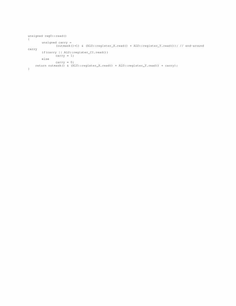
unsigned regU::read(){
unsigned carry = (outmask()+1) & (ALU::register_X.read() + ALU::register_Y.read()); // end-around
carryif(carry || ALU::register_CI.read())
carry = 1; else
carry = 0; return outmask() & (ALU::register_X.read() + ALU::register_Y.read() + carry);}

BUS (BUS.h)
/**************************************************************************** * BUS - READ/WRITE BUS subsystem * * AUTHOR: John Pultorak * DATE: 9/22/01 * FILE: BUS.h * * VERSIONS: * * DESCRIPTION: * RW Bus for the Block 1 Apollo Guidance Computer prototype (AGC4). * * SOURCES: * Mostly based on information from "Logical Description for the Apollo * Guidance Computer (AGC4)", Albert Hopkins, Ramon Alonso, and Hugh * Blair-Smith, R-393, MIT Instrumentation Laboratory, 1963. * * NOTES: * ***************************************************************************** */#ifndef BUS_H#define BUS_H
// BUS LINE DESIGNATIONS// Specify the assignment of bus lines to the inputs of a register (for a 'write'// operation into a register). Each 'conv_' array specifies the inputs into a// single register. The index into the array corresponds to the bit position in// the register, where the first parameter (index=0) is bit 16 of the register (msb)// and the last parameter (index=15) is register bit 1 (lsb). The value of// the parameter identifies the bus line assigned to that register bit. 'BX'// means 'don't care'; i.e.: leave that register bit alone.
enum { D0=17, // force bit to zeroSGM=15, // sign bit in memorySG=16, // sign (S2; one's compliment)US=15, // uncorrected sign (S1; overflow), except in register GB14=14, B13=13, B12=12, B11=11, B10=10, B9=9, B8=8, B7=7, B6=6, B5=5, B4=4, B3=3, B2=2, B1=1, BX=0 // ignore
};
enum ovfState { NO_OVF, POS_OVF, NEG_OVF };
class BUS{public:
static unsigned glbl_READ_BUS; // read/write bus for xfer between central regsstatic unsigned glbl_WRITE_BUS; // read/write bus for xfer between central regs
friend class INT;friend class CTR;
private:static ovfState testOverflow(unsigned bus);
};
#endif

BUS (BUS.cpp)
/**************************************************************************** * BUS - READ/WRITE BUS subsystem * * AUTHOR: John Pultorak * DATE: 9/22/01 * FILE: BUS.cpp * * NOTES: see header file. * ***************************************************************************** */#include "BUS.h"
unsigned BUS::glbl_READ_BUS = 0;unsigned BUS::glbl_WRITE_BUS = 0;
ovfState BUS::testOverflow(unsigned bus){
if((bus & 0100000) && !(bus & 0040000))return NEG_OVF; // negative overflow
else if(!(bus & 0100000) && (bus & 0040000))return POS_OVF; // positive overflow
elsereturn NO_OVF;
}
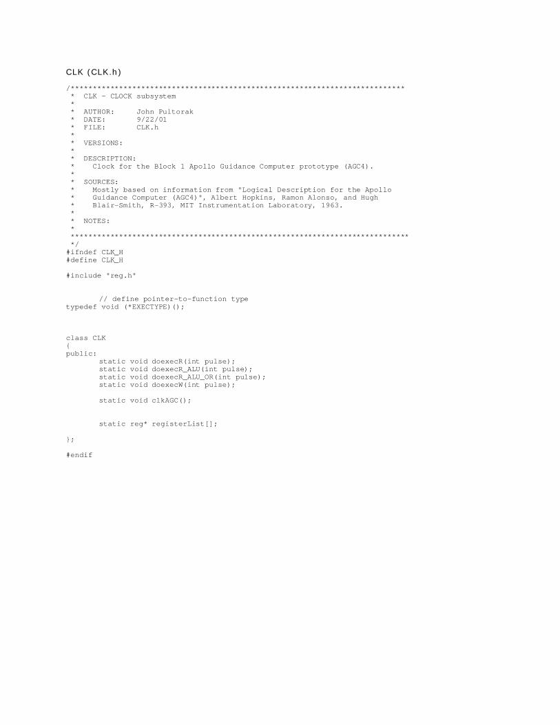
CLK (CLK.h)
/**************************************************************************** * CLK - CLOCK subsystem * * AUTHOR: John Pultorak * DATE: 9/22/01 * FILE: CLK.h * * VERSIONS: * * DESCRIPTION: * Clock for the Block 1 Apollo Guidance Computer prototype (AGC4). * * SOURCES: * Mostly based on information from "Logical Description for the Apollo * Guidance Computer (AGC4)", Albert Hopkins, Ramon Alonso, and Hugh * Blair-Smith, R-393, MIT Instrumentation Laboratory, 1963. * * NOTES: * ***************************************************************************** */#ifndef CLK_H#define CLK_H
#include "reg.h"
// define pointer-to-function typetypedef void (*EXECTYPE)();
class CLK{public:
static void doexecR(int pulse);static void doexecR_ALU(int pulse);static void doexecR_ALU_OR(int pulse);static void doexecW(int pulse);
static void clkAGC();
static reg* registerList[];
};
#endif

CLK (CLK.cpp)
/**************************************************************************** * CLK - CLOCK subsystem * * AUTHOR: John Pultorak * DATE: 9/22/01 * FILE: CLK.cpp * * NOTES: see header file. * ***************************************************************************** */#include "CLK.h"#include "INP.h"#include "OUT.h"#include "MBF.h"#include "ADR.h"#include "SEQ.h"#include "ALU.h"#include "CRG.h"#include "CTR.h"#include "INT.h"#include "PAR.h"#include "TPG.h"#include "SCL.h"#include "MEM.h"
// A container for all registers. This is kept so we can iterate through// all registers to execute the control pulses. For simulation purposes// only; this has no counterpart in the hardware AGC.
reg* CLK::registerList[] = // registers are in no particular sequence{
&INP::register_IN0, &INP::register_IN1, &INP::register_IN2, &INP::register_IN3,&OUT::register_OUT1, &OUT::register_OUT2, &OUT::register_OUT3, &OUT::register_OUT4,&MBF::register_G, &PAR::register_G15, &ADR::register_S, &ADR::register_BNK,
&SEQ::register_SQ, &ALU::register_B,&CRG::register_Q, &CRG::register_Z, &CRG::register_LP, &CRG::register_A, &ALU::register_X,&ALU::register_Y, &ALU::register_U, &SEQ::register_STA, &SEQ::register_STB, &SEQ::register_SNI,&SEQ::register_LOOPCTR, &ALU::register_CI, &SEQ::register_BR1, &SEQ::register_BR2, &CTR::register_UpCELL, &CTR::register_DnCELL,&INT::register_RPCELL, &INT::register_INHINT1, &INT::register_INHINT,&PAR::register_P, &PAR::register_P2, &PAR::register_PALM,&TPG::register_SG,&SCL::register_SCL,&SCL::register_F17, &SCL::register_F13, &SCL::register_F10,0 // zero is end-of-list flag
};
void CLK::clkAGC(){
// Now that all the inputs are set up, clock the registers so the outputs// can change state in accordance with the inputs.
for(int i=0; registerList[i]; i++){
registerList[i]->clk();}
}
void execR_NOPULSE() { }void execR_RA0() { CRG::execRP_RA0(); }void execR_RA1() { CRG::execRP_RA1(); }void execR_RA2() { CRG::execRP_RA2(); }void execR_RA3() { CRG::execRP_RA3(); }void execR_RA4() { INP::execRP_RA4(); }void execR_RA5() { INP::execRP_RA5(); }void execR_RA6() { INP::execRP_RA6(); }

void execR_RA7() { INP::execRP_RA7(); }void execR_RA11() { OUT::execRP_RA11(); }void execR_RA12() { OUT::execRP_RA12(); }void execR_RA13() { OUT::execRP_RA13(); }void execR_RA14() { OUT::execRP_RA14(); }void execR_RA() { CRG::execRP_RA(); }void execR_RBK() { ADR::execRP_RBK(); }void execR_RG() { MBF::execRP_RG(); }void execR_RLP() { CRG::execRP_RLP(); }void execR_RQ() { CRG::execRP_RQ(); }void execR_RRPA() { INT::execRP_RRPA(); }void execR_RSCT() { CTR::execRP_RSCT(); }void execR_RZ() { CRG::execRP_RZ(); }void execR_SBWG() { MEM::execRP_SBWG(); }void execR_WE() { MBF::execRP_WE(); PAR::execRP_WE(); }
void execR_ALU_RB() { ALU::execRP_ALU_RB(); }void execR_ALU_RC() { ALU::execRP_ALU_RC(); }void execR_ALU_RU() { ALU::execRP_ALU_RU(); }
void execR_ALU_OR_RSB() { ALU::execRP_ALU_OR_RSB(); }void execR_ALU_OR_R1() { ALU::execRP_ALU_OR_R1(); }void execR_ALU_OR_R1C() { ALU::execRP_ALU_OR_R1C(); }void execR_ALU_OR_R2() { ALU::execRP_ALU_OR_R2(); }void execR_ALU_OR_R22() { ALU::execRP_ALU_OR_R22(); }void execR_ALU_OR_R24() { ALU::execRP_ALU_OR_R24(); }void execR_ALU_OR_R2000() { ALU::execRP_ALU_OR_R2000(); }void execR_ALU_OR_RB14() { ALU::execRP_ALU_OR_RB14(); }
EXECTYPE execR[] ={
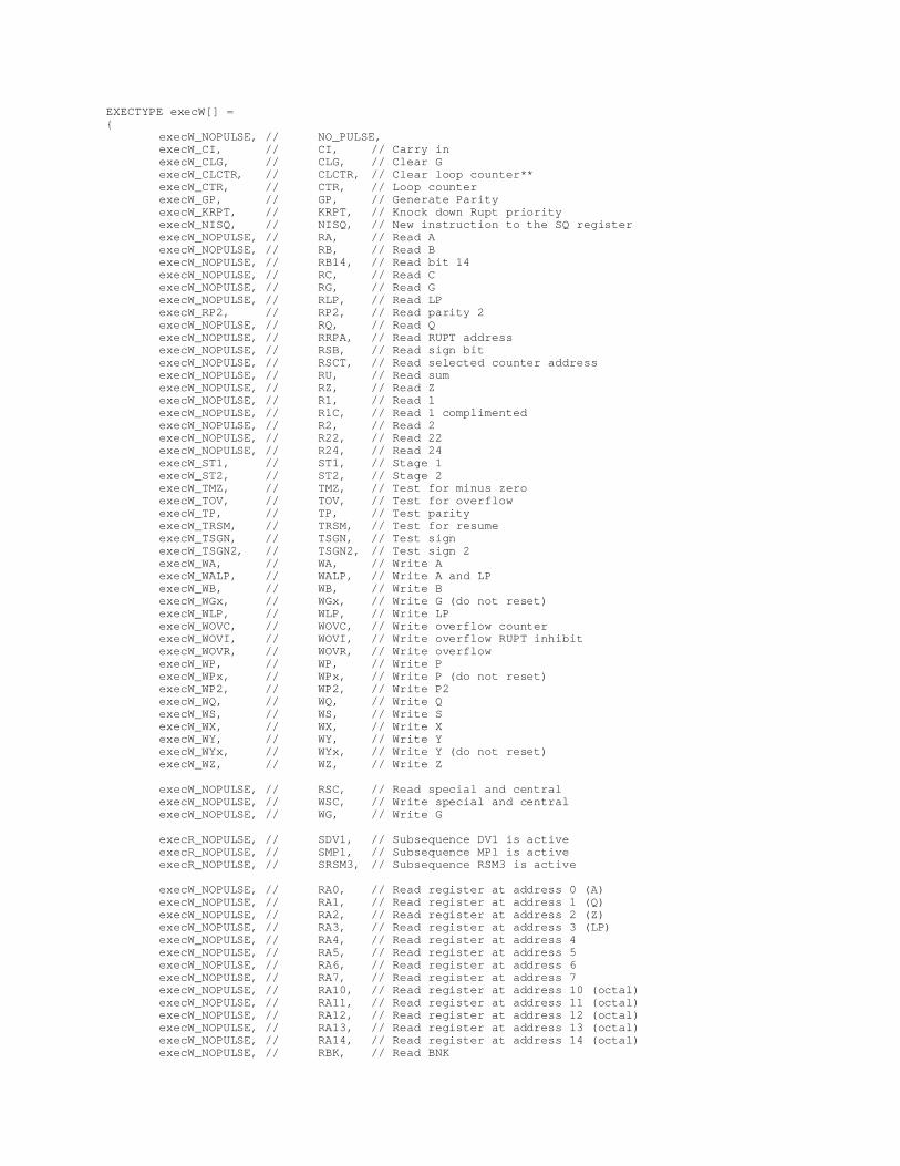
execR_NOPULSE, // NO_PULSE,execR_NOPULSE, // CI, // Carry inexecR_NOPULSE, // CLG, // Clear GexecR_NOPULSE, // CLCTR, // Clear loop counter**execR_NOPULSE, // CTR, // Loop counterexecR_NOPULSE, // GP, // Generate ParityexecR_NOPULSE, // KRPT, // Knock down Rupt priorityexecR_NOPULSE, // NISQ, // New instruction to the SQ registerexecR_RA, // RA, // Read AexecR_NOPULSE, // RB, // Read BexecR_NOPULSE, // RB14, // Read bit 14execR_NOPULSE, // RC, // Read CexecR_RG, // RG, // Read GexecR_RLP, // RLP, // Read LPexecR_NOPULSE, // RP2, // Read parity 2execR_RQ, // RQ, // Read QexecR_RRPA, // RRPA, // Read RUPT addressexecR_NOPULSE, // RSB, // Read sign bitexecR_RSCT, // RSCT, // Read selected counter addressexecR_NOPULSE, // RU, // Read sumexecR_RZ, // RZ, // Read ZexecR_NOPULSE, // R1, // Read 1execR_NOPULSE, // R1C, // Read 1 complimentedexecR_NOPULSE, // R2, // Read 2execR_NOPULSE, // R22, // Read 22execR_NOPULSE, // R24, // Read 24execR_NOPULSE, // ST1, // Stage 1execR_NOPULSE, // ST2, // Stage 2execR_NOPULSE, // TMZ, // Test for minus zeroexecR_NOPULSE, // TOV, // Test for overflowexecR_NOPULSE, // TP, // Test parityexecR_NOPULSE, // TRSM, // Test for resumeexecR_NOPULSE, // TSGN, // Test signexecR_NOPULSE, // TSGN2, // Test sign 2execR_NOPULSE, // WA, // Write AexecR_NOPULSE, // WALP, // Write A and LPexecR_NOPULSE, // WB, // Write BexecR_NOPULSE, // WGx, // Write G (do not reset)execR_NOPULSE, // WLP, // Write LPexecR_NOPULSE, // WOVC, // Write overflow counterexecR_NOPULSE, // WOVI, // Write overflow RUPT inhibitexecR_NOPULSE, // WOVR, // Write overflowexecR_NOPULSE, // WP, // Write P
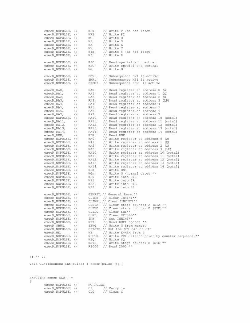
execR_NOPULSE, // WPx, // Write P (do not reset)execR_NOPULSE, // WP2, // Write P2execR_NOPULSE, // WQ, // Write QexecR_NOPULSE, // WS, // Write SexecR_NOPULSE, // WX, // Write XexecR_NOPULSE, // WY, // Write YexecR_NOPULSE, // WYx, // Write Y (do not reset)execR_NOPULSE, // WZ, // Write Z
execR_NOPULSE, // RSC, // Read special and centralexecR_NOPULSE, // WSC, // Write special and centralexecR_NOPULSE, // WG, // Write G
execR_NOPULSE, // SDV1, // Subsequence DV1 is activeexecR_NOPULSE, // SMP1, // Subsequence MP1 is activeexecR_NOPULSE, // SRSM3, // Subsequence RSM3 is active
execR_RA0, // RA0, // Read register at address 0 (A)execR_RA1, // RA1, // Read register at address 1 (Q)execR_RA2, // RA2, // Read register at address 2 (Z)execR_RA3, // RA3, // Read register at address 3 (LP)execR_RA4, // RA4, // Read register at address 4execR_RA5, // RA5, // Read register at address 5execR_RA6, // RA6, // Read register at address 6execR_RA7, // RA7, // Read register at address 7execR_NOPULSE, // RA10, // Read register at address 10 (octal)execR_RA11, // RA11, // Read register at address 11 (octal)execR_RA12, // RA12, // Read register at address 12 (octal)execR_RA13, // RA13, // Read register at address 13 (octal)execR_RA14, // RA14, // Read register at address 14 (octal)execR_RBK, // RBK, // Read BNKexecR_NOPULSE, // WA0, // Write register at address 0 (A)execR_NOPULSE, // WA1, // Write register at address 1 (Q)execR_NOPULSE, // WA2, // Write register at address 2 (Z)execR_NOPULSE, // WA3, // Write register at address 3 (LP)execR_NOPULSE, // WA10, // Write register at address 10 (octal)execR_NOPULSE, // WA11, // Write register at address 11 (octal)execR_NOPULSE, // WA12, // Write register at address 12 (octal)execR_NOPULSE, // WA13, // Write register at address 13 (octal)execR_NOPULSE, // WA14, // Write register at address 14 (octal)execR_NOPULSE, // WBK, // Write BNKexecR_NOPULSE, // WGn, // Write G (normal gates)**execR_NOPULSE, // W20, // Write into CYRexecR_NOPULSE, // W21, // Write into SRexecR_NOPULSE, // W22, // Write into CYLexecR_NOPULSE, // W23 // Write into SL
execR_NOPULSE, // GENRST,// General Reset**execR_NOPULSE, // CLINH, // Clear INHINT**execR_NOPULSE, // CLINH1,// Clear INHINT1**execR_NOPULSE, // CLSTA, // Clear state counter A (STA)**execR_NOPULSE, // CLSTB, // Clear state counter B (STB)**execR_NOPULSE, // CLISQ, // Clear SNI**execR_NOPULSE, // CLRP, // Clear RPCELL**execR_NOPULSE, // INH, // Set INHINT**execR_NOPULSE, // RPT, // Read RUPT opcode **execR_SBWG, // SBWG, // Write G from memoryexecR_NOPULSE, // SETSTB,// Set the ST1 bit of STBexecR_WE, // WE, // Write E-MEM from GexecR_NOPULSE, // WPCTR, // Write PCTR (latch priority counter sequence)**execR_NOPULSE, // WSQ, // Write SQexecR_NOPULSE, // WSTB, // Write stage counter B (STB)**execR_NOPULSE, // R2000, // Read 2000 **
}; // 99
void CLK::doexecR(int pulse) { execR[pulse](); }
EXECTYPE execR_ALU[] ={
execR_NOPULSE, // NO_PULSE,execR_NOPULSE, // CI, // Carry inexecR_NOPULSE, // CLG, // Clear G

execR_NOPULSE, // CLCTR, // Clear loop counter**execR_NOPULSE, // CTR, // Loop counterexecR_NOPULSE, // GP, // Generate ParityexecR_NOPULSE, // KRPT, // Knock down Rupt priorityexecR_NOPULSE, // NISQ, // New instruction to the SQ registerexecR_NOPULSE, // RA, // Read AexecR_ALU_RB, // RB, // Read BexecR_NOPULSE, // RB14, // Read bit 14execR_ALU_RC, // RC, // Read CexecR_NOPULSE, // RG, // Read GexecR_NOPULSE, // RLP, // Read LPexecR_NOPULSE, // RP2, // Read parity 2execR_NOPULSE, // RQ, // Read QexecR_NOPULSE, // RRPA, // Read RUPT addressexecR_NOPULSE, // RSB, // Read sign bitexecR_NOPULSE, // RSCT, // Read selected counter addressexecR_ALU_RU, // RU, // Read sumexecR_NOPULSE, // RZ, // Read ZexecR_NOPULSE, // R1, // Read 1execR_NOPULSE, // R1C, // Read 1 complimentedexecR_NOPULSE, // R2, // Read 2execR_NOPULSE, // R22, // Read 22execR_NOPULSE, // R24, // Read 24execR_NOPULSE, // ST1, // Stage 1execR_NOPULSE, // ST2, // Stage 2execR_NOPULSE, // TMZ, // Test for minus zeroexecR_NOPULSE, // TOV, // Test for overflowexecR_NOPULSE, // TP, // Test parityexecR_NOPULSE, // TRSM, // Test for resumeexecR_NOPULSE, // TSGN, // Test signexecR_NOPULSE, // TSGN2, // Test sign 2execR_NOPULSE, // WA, // Write AexecR_NOPULSE, // WALP, // Write A and LPexecR_NOPULSE, // WB, // Write BexecR_NOPULSE, // WGx, // Write G (do not reset)execR_NOPULSE, // WLP, // Write LPexecR_NOPULSE, // WOVC, // Write overflow counterexecR_NOPULSE, // WOVI, // Write overflow RUPT inhibitexecR_NOPULSE, // WOVR, // Write overflowexecR_NOPULSE, // WP, // Write PexecR_NOPULSE, // WPx, // Write P (do not reset)execR_NOPULSE, // WP2, // Write P2execR_NOPULSE, // WQ, // Write QexecR_NOPULSE, // WS, // Write SexecR_NOPULSE, // WX, // Write XexecR_NOPULSE, // WY, // Write YexecR_NOPULSE, // WYx, // Write Y (do not reset)execR_NOPULSE, // WZ, // Write Z
execR_NOPULSE, // RSC, // Read special and centralexecR_NOPULSE, // WSC, // Write special and centralexecR_NOPULSE, // WG, // Write G
execR_NOPULSE, // SDV1, // Subsequence DV1 is activeexecR_NOPULSE, // SMP1, // Subsequence MP1 is activeexecR_NOPULSE, // SRSM3, // Subsequence RSM3 is active
execR_NOPULSE, // RA0, // Read register at address 0 (A)execR_NOPULSE, // RA1, // Read register at address 1 (Q)execR_NOPULSE, // RA2, // Read register at address 2 (Z)execR_NOPULSE, // RA3, // Read register at address 3 (LP)execR_NOPULSE, // RA4, // Read register at address 4execR_NOPULSE, // RA5, // Read register at address 5execR_NOPULSE, // RA6, // Read register at address 6execR_NOPULSE, // RA7, // Read register at address 7execR_NOPULSE, // RA10, // Read register at address 10 (octal)execR_NOPULSE, // RA11, // Read register at address 11 (octal)execR_NOPULSE, // RA12, // Read register at address 12 (octal)execR_NOPULSE, // RA13, // Read register at address 13 (octal)execR_NOPULSE, // RA14, // Read register at address 14 (octal)execR_NOPULSE, // RBK, // Read BNKexecR_NOPULSE, // WA0, // Write register at address 0 (A)execR_NOPULSE, // WA1, // Write register at address 1 (Q)execR_NOPULSE, // WA2, // Write register at address 2 (Z)execR_NOPULSE, // WA3, // Write register at address 3 (LP)execR_NOPULSE, // WA10, // Write register at address 10 (octal)

execR_NOPULSE, // WA11, // Write register at address 11 (octal)execR_NOPULSE, // WA12, // Write register at address 12 (octal)execR_NOPULSE, // WA13, // Write register at address 13 (octal)execR_NOPULSE, // WA14, // Write register at address 14 (octal)execR_NOPULSE, // WBK, // Write BNKexecR_NOPULSE, // WGn, // Write G (normal gates)**execR_NOPULSE, // W20, // Write into CYRexecR_NOPULSE, // W21, // Write into SRexecR_NOPULSE, // W22, // Write into CYLexecR_NOPULSE, // W23 // Write into SL
execR_NOPULSE, // GENRST,// General Reset**execR_NOPULSE, // CLINH, // Clear INHINT**execR_NOPULSE, // CLINH1,// Clear INHINT1**execR_NOPULSE, // CLSTA, // Clear state counter A (STA)**execR_NOPULSE, // CLSTB, // Clear state counter B (STB)**execR_NOPULSE, // CLISQ, // Clear SNI**execR_NOPULSE, // CLRP, // Clear RPCELL**execR_NOPULSE, // INH, // Set INHINT**execR_NOPULSE, // RPT, // Read RUPT opcode **execR_NOPULSE, // SBWG, // Write G from memoryexecR_NOPULSE, // SETSTB,// Set the ST1 bit of STBexecR_NOPULSE, // WE, // Write E-MEM from GexecR_NOPULSE, // WPCTR, // Write PCTR (latch priority counter sequence)**execR_NOPULSE, // WSQ, // Write SQexecR_NOPULSE, // WSTB, // Write stage counter B (STB)**execR_NOPULSE, // R2000, // Read 2000 **
};
void CLK::doexecR_ALU(int pulse) { execR_ALU[pulse](); }
EXECTYPE execR_ALU_OR[] ={
execR_NOPULSE, // NO_PULSE,execR_NOPULSE, // CI, // Carry inexecR_NOPULSE, // CLG, // Clear GexecR_NOPULSE, // CLCTR, // Clear loop counter**execR_NOPULSE, // CTR, // Loop counterexecR_NOPULSE, // GP, // Generate ParityexecR_NOPULSE, // KRPT, // Knock down Rupt priorityexecR_NOPULSE, // NISQ, // New instruction to the SQ registerexecR_NOPULSE, // RA, // Read AexecR_NOPULSE, // RB, // Read BexecR_ALU_OR_RB14, // RB14, // Read bit 14execR_NOPULSE, // RC, // Read CexecR_NOPULSE, // RG, // Read GexecR_NOPULSE, // RLP, // Read LPexecR_NOPULSE, // RP2, // Read parity 2execR_NOPULSE, // RQ, // Read QexecR_NOPULSE, // RRPA, // Read RUPT addressexecR_ALU_OR_RSB, // RSB, // Read sign bitexecR_NOPULSE, // RSCT, // Read selected counter addressexecR_NOPULSE, // RU, // Read sumexecR_NOPULSE, // RZ, // Read ZexecR_ALU_OR_R1, // R1, // Read 1execR_ALU_OR_R1C, // R1C, // Read 1 complimentedexecR_ALU_OR_R2, // R2, // Read 2execR_ALU_OR_R22, // R22, // Read 22execR_ALU_OR_R24, // R24, // Read 24execR_NOPULSE, // ST1, // Stage 1execR_NOPULSE, // ST2, // Stage 2execR_NOPULSE, // TMZ, // Test for minus zeroexecR_NOPULSE, // TOV, // Test for overflowexecR_NOPULSE, // TP, // Test parityexecR_NOPULSE, // TRSM, // Test for resumeexecR_NOPULSE, // TSGN, // Test signexecR_NOPULSE, // TSGN2, // Test sign 2execR_NOPULSE, // WA, // Write AexecR_NOPULSE, // WALP, // Write A and LPexecR_NOPULSE, // WB, // Write BexecR_NOPULSE, // WGx, // Write G (do not reset)execR_NOPULSE, // WLP, // Write LP

execR_NOPULSE, // WOVC, // Write overflow counterexecR_NOPULSE, // WOVI, // Write overflow RUPT inhibitexecR_NOPULSE, // WOVR, // Write overflowexecR_NOPULSE, // WP, // Write PexecR_NOPULSE, // WPx, // Write P (do not reset)execR_NOPULSE, // WP2, // Write P2execR_NOPULSE, // WQ, // Write QexecR_NOPULSE, // WS, // Write SexecR_NOPULSE, // WX, // Write XexecR_NOPULSE, // WY, // Write YexecR_NOPULSE, // WYx, // Write Y (do not reset)execR_NOPULSE, // WZ, // Write Z
execR_NOPULSE, // RSC, // Read special and centralexecR_NOPULSE, // WSC, // Write special and centralexecR_NOPULSE, // WG, // Write G
execR_NOPULSE, // SDV1, // Subsequence DV1 is activeexecR_NOPULSE, // SMP1, // Subsequence MP1 is activeexecR_NOPULSE, // SRSM3, // Subsequence RSM3 is active
execR_NOPULSE, // RA0, // Read register at address 0 (A)execR_NOPULSE, // RA1, // Read register at address 1 (Q)execR_NOPULSE, // RA2, // Read register at address 2 (Z)execR_NOPULSE, // RA3, // Read register at address 3 (LP)execR_NOPULSE, // RA4, // Read register at address 4execR_NOPULSE, // RA5, // Read register at address 5execR_NOPULSE, // RA6, // Read register at address 6execR_NOPULSE, // RA7, // Read register at address 7execR_NOPULSE, // RA10, // Read register at address 10 (octal)execR_NOPULSE, // RA11, // Read register at address 11 (octal)execR_NOPULSE, // RA12, // Read register at address 12 (octal)execR_NOPULSE, // RA13, // Read register at address 13 (octal)execR_NOPULSE, // RA14, // Read register at address 14 (octal)execR_NOPULSE, // RBK, // Read BNKexecR_NOPULSE, // WA0, // Write register at address 0 (A)execR_NOPULSE, // WA1, // Write register at address 1 (Q)execR_NOPULSE, // WA2, // Write register at address 2 (Z)execR_NOPULSE, // WA3, // Write register at address 3 (LP)execR_NOPULSE, // WA10, // Write register at address 10 (octal)execR_NOPULSE, // WA11, // Write register at address 11 (octal)execR_NOPULSE, // WA12, // Write register at address 12 (octal)execR_NOPULSE, // WA13, // Write register at address 13 (octal)execR_NOPULSE, // WA14, // Write register at address 14 (octal)execR_NOPULSE, // WBK, // Write BNKexecR_NOPULSE, // WGn, // Write G (normal gates)**execR_NOPULSE, // W20, // Write into CYRexecR_NOPULSE, // W21, // Write into SRexecR_NOPULSE, // W22, // Write into CYLexecR_NOPULSE, // W23 // Write into SL
execR_NOPULSE, // GENRST,// General Reset**execR_NOPULSE, // CLINH, // Clear INHINT**execR_NOPULSE, // CLINH1,// Clear INHINT1**execR_NOPULSE, // CLSTA, // Clear state counter A (STA)**execR_NOPULSE, // CLSTB, // Clear state counter B (STB)**execR_NOPULSE, // CLISQ, // Clear SNI**execR_NOPULSE, // CLRP, // Clear RPCELL**execR_NOPULSE, // INH, // Set INHINT**execR_NOPULSE, // RPT, // Read RUPT opcode **execR_NOPULSE, // SBWG, // Write G from memoryexecR_NOPULSE, // SETSTB,// Set the ST1 bit of STBexecR_NOPULSE, // WE, // Write E-MEM from GexecR_NOPULSE, // WPCTR, // Write PCTR (latch priority counter sequence)**execR_NOPULSE, // WSQ, // Write SQexecR_NOPULSE, // WSTB, // Write stage counter B (STB)**execR_ALU_OR_R2000, // R2000, // Read 2000 **
};
void CLK::doexecR_ALU_OR(int pulse) { execR_ALU_OR[pulse](); }

void execW_NOPULSE() { }void execW_CI() { ALU::execWP_CI(); }void execW_CLG() { PAR::execWP_CLG(); }void execW_CLINH() { INT::execWP_CLINH(); }void execW_CLINH1() { INT::execWP_CLINH1(); }void execW_CLISQ() { SEQ::execWP_CLISQ(); }void execW_CLCTR() { SEQ::execWP_CLCTR(); }void execW_CLRP() { INT::execWP_CLRP(); }void execW_CLSTA() { SEQ::execWP_CLSTA(); }void execW_CLSTB() { SEQ::execWP_CLSTB(); }void execW_CTR() { SEQ::execWP_CTR(); }
void execW_GENRST() { SEQ::execWP_GENRST(); MBF::execWP_GENRST(); CRG::execWP_GENRST(); PAR::execWP_GENRST(); ALU::execWP_GENRST(); CTR::execWP_GENRST(); INT::execWP_GENRST(); OUT::execWP_GENRST(); }
void execW_GP() { PAR::execWP_GP(); }void execW_INH() { INT::execWP_INH(); }void execW_KRPT() { INT::execWP_KRPT(); }void execW_NISQ() { SEQ::execWP_NISQ(); }void execW_RPT() { INT::execWP_RPT(); }void execW_RP2() { PAR::execWP_RP2(); }void execW_SBWG() { MBF::execWP_SBWG(); PAR::execWP_SBWG(); }void execW_SETSTB() { SEQ::execWP_SETSTB(); }void execW_ST1() { SEQ::execWP_ST1(); }void execW_ST2() { SEQ::execWP_ST2(); }void execW_TMZ() { SEQ::execWP_TMZ(); }void execW_TOV() { SEQ::execWP_TOV(); }void execW_TP() { PAR::execWP_TP(); }void execW_TRSM() { SEQ::execWP_TRSM(); }void execW_TSGN() { SEQ::execWP_TSGN(); }void execW_TSGN2() { SEQ::execWP_TSGN2(); }void execW_WA0() { CRG::execWP_WA0(); }void execW_WA1() { CRG::execWP_WA1(); }void execW_WA2() { CRG::execWP_WA2(); }void execW_WA3() { CRG::execWP_WA3(); }void execW_WA10() { OUT::execWP_WA10(); }void execW_WA11() { OUT::execWP_WA11(); }void execW_WA12() { OUT::execWP_WA12(); }void execW_WA13() { OUT::execWP_WA13(); }void execW_WA14() { OUT::execWP_WA14(); }void execW_WA() { CRG::execWP_WA(); }void execW_WALP() { CRG::execWP_WALP(); }void execW_WB() { ALU::execWP_WB(); }void execW_WBK() { ADR::execWP_WBK(); }void execW_WE() { MEM::execWP_WE(); }void execW_WGn() { MBF::execWP_WGn(); }void execW_WGx() { MBF::execWP_WGx(); PAR::execWP_WGx(); }void execW_WLP() { CRG::execWP_WLP(); }void execW_WOVC() { CTR::execWP_WOVC(); }void execW_WOVI() { INT::execWP_WOVI(); }void execW_WOVR() { CTR::execWP_WOVR(); }void execW_WP() { PAR::execWP_WP(); }void execW_WPx() { PAR::execWP_WPx(); }void execW_WP2() { PAR::execWP_WP2(); }void execW_WPCTR() { CTR::execWP_WPCTR(); }void execW_WQ() { CRG::execWP_WQ(); }void execW_WS() { ADR::execWP_WS(); }void execW_WSQ() { SEQ::execWP_WSQ(); }void execW_WSTB() { SEQ::execWP_WSTB(); }void execW_WX() { ALU::execWP_WX(); }void execW_WY() { ALU::execWP_WY(); }void execW_WYx() { ALU::execWP_WYx(); }void execW_WZ() { CRG::execWP_WZ(); }void execW_W20() { MBF::execWP_W20(); }void execW_W21() { MBF::execWP_W21(); }void execW_W22() { MBF::execWP_W22(); }void execW_W23() { MBF::execWP_W23(); }
EXECTYPE execW[] ={
execW_NOPULSE, // NO_PULSE,execW_CI, // CI, // Carry inexecW_CLG, // CLG, // Clear GexecW_CLCTR, // CLCTR, // Clear loop counter**execW_CTR, // CTR, // Loop counterexecW_GP, // GP, // Generate ParityexecW_KRPT, // KRPT, // Knock down Rupt priorityexecW_NISQ, // NISQ, // New instruction to the SQ registerexecW_NOPULSE, // RA, // Read AexecW_NOPULSE, // RB, // Read BexecW_NOPULSE, // RB14, // Read bit 14execW_NOPULSE, // RC, // Read CexecW_NOPULSE, // RG, // Read GexecW_NOPULSE, // RLP, // Read LPexecW_RP2, // RP2, // Read parity 2execW_NOPULSE, // RQ, // Read QexecW_NOPULSE, // RRPA, // Read RUPT addressexecW_NOPULSE, // RSB, // Read sign bitexecW_NOPULSE, // RSCT, // Read selected counter addressexecW_NOPULSE, // RU, // Read sumexecW_NOPULSE, // RZ, // Read ZexecW_NOPULSE, // R1, // Read 1execW_NOPULSE, // R1C, // Read 1 complimentedexecW_NOPULSE, // R2, // Read 2execW_NOPULSE, // R22, // Read 22execW_NOPULSE, // R24, // Read 24execW_ST1, // ST1, // Stage 1execW_ST2, // ST2, // Stage 2execW_TMZ, // TMZ, // Test for minus zeroexecW_TOV, // TOV, // Test for overflowexecW_TP, // TP, // Test parityexecW_TRSM, // TRSM, // Test for resumeexecW_TSGN, // TSGN, // Test signexecW_TSGN2, // TSGN2, // Test sign 2execW_WA, // WA, // Write AexecW_WALP, // WALP, // Write A and LPexecW_WB, // WB, // Write BexecW_WGx, // WGx, // Write G (do not reset)execW_WLP, // WLP, // Write LPexecW_WOVC, // WOVC, // Write overflow counterexecW_WOVI, // WOVI, // Write overflow RUPT inhibitexecW_WOVR, // WOVR, // Write overflowexecW_WP, // WP, // Write PexecW_WPx, // WPx, // Write P (do not reset)execW_WP2, // WP2, // Write P2execW_WQ, // WQ, // Write QexecW_WS, // WS, // Write SexecW_WX, // WX, // Write XexecW_WY, // WY, // Write YexecW_WYx, // WYx, // Write Y (do not reset)execW_WZ, // WZ, // Write Z
execW_NOPULSE, // RSC, // Read special and centralexecW_NOPULSE, // WSC, // Write special and centralexecW_NOPULSE, // WG, // Write G
execR_NOPULSE, // SDV1, // Subsequence DV1 is activeexecR_NOPULSE, // SMP1, // Subsequence MP1 is activeexecR_NOPULSE, // SRSM3, // Subsequence RSM3 is active
execW_NOPULSE, // RA0, // Read register at address 0 (A)execW_NOPULSE, // RA1, // Read register at address 1 (Q)execW_NOPULSE, // RA2, // Read register at address 2 (Z)execW_NOPULSE, // RA3, // Read register at address 3 (LP)execW_NOPULSE, // RA4, // Read register at address 4execW_NOPULSE, // RA5, // Read register at address 5execW_NOPULSE, // RA6, // Read register at address 6execW_NOPULSE, // RA7, // Read register at address 7execW_NOPULSE, // RA10, // Read register at address 10 (octal)execW_NOPULSE, // RA11, // Read register at address 11 (octal)execW_NOPULSE, // RA12, // Read register at address 12 (octal)execW_NOPULSE, // RA13, // Read register at address 13 (octal)execW_NOPULSE, // RA14, // Read register at address 14 (octal)execW_NOPULSE, // RBK, // Read BNK

execW_WA0, // WA0, // Write register at address 0 (A)execW_WA1, // WA1, // Write register at address 1 (Q)execW_WA2, // WA2, // Write register at address 2 (Z)execW_WA3, // WA3, // Write register at address 3 (LP)execW_WA10, // WA10, // Write register at address 10 (octal)execW_WA11, // WA11, // Write register at address 11 (octal)execW_WA12, // WA12, // Write register at address 12 (octal)execW_WA13, // WA13, // Write register at address 13 (octal)execW_WA14, // WA14, // Write register at address 14 (octal)execW_WBK, // WBK, // Write BNKexecW_WGn, // WGn, // Write G (normal gates)**execW_W20, // W20, // Write into CYRexecW_W21, // W21, // Write into SRexecW_W22, // W22, // Write into CYLexecW_W23, // W23 // Write into SL
execW_GENRST, // GENRST,// General Reset**execW_CLINH, // CLINH, // Clear INHINT**execW_CLINH1, // CLINH1,// Clear INHINT1**execW_CLSTA, // CLSTA, // Clear state counter A (STA)**execW_CLSTB, // CLSTB, // Clear state counter B (STB)**execW_CLISQ, // CLISQ, // Clear SNI**execW_CLRP, // CLRP, // Clear RPCELL**execW_INH, // INH, // Set INHINT**execW_RPT, // RPT, // Read RUPT opcode **execW_SBWG, // SBWG, // Write G from memoryexecW_SETSTB, // SETSTB,// Set the ST1 bit of STBexecW_WE, // WE, // Write E-MEM from GexecW_WPCTR, // WPCTR, // Write PCTR (latch priority counter sequence)**execW_WSQ, // WSQ, // Write SQexecW_WSTB, // WSTB, // Write stage counter B (STB)**execW_NOPULSE, // R2000, // Read 2000 **
}; // 99
void CLK::doexecW(int pulse) { execW[pulse](); }
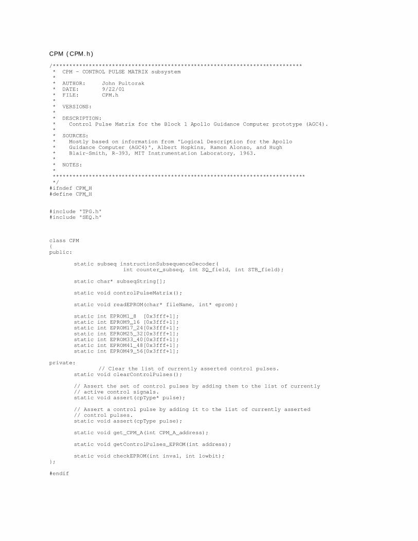
CPM (CPM.h)
/**************************************************************************** * CPM - CONTROL PULSE MATRIX subsystem * * AUTHOR: John Pultorak * DATE: 9/22/01 * FILE: CPM.h * * VERSIONS: * * DESCRIPTION: * Control Pulse Matrix for the Block 1 Apollo Guidance Computer prototype (AGC4). * * SOURCES: * Mostly based on information from "Logical Description for the Apollo * Guidance Computer (AGC4)", Albert Hopkins, Ramon Alonso, and Hugh * Blair-Smith, R-393, MIT Instrumentation Laboratory, 1963. * * NOTES: * ***************************************************************************** */#ifndef CPM_H#define CPM_H
#include "TPG.h"#include "SEQ.h"
class CPM{public:
static subseq instructionSubsequenceDecoder(int counter_subseq, int SQ_field, int STB_field);
static char* subseqString[];
static void controlPulseMatrix();
static void readEPROM(char* fileName, int* eprom);
static int EPROM1_8 [0x3fff+1];static int EPROM9_16 [0x3fff+1];static int EPROM17_24[0x3fff+1];static int EPROM25_32[0x3fff+1];static int EPROM33_40[0x3fff+1];static int EPROM41_48[0x3fff+1];static int EPROM49_56[0x3fff+1];
private:// Clear the list of currently asserted control pulses.
static void clearControlPulses();
// Assert the set of control pulses by adding them to the list of currently// active control signals.static void assert(cpType* pulse);
// Assert a control pulse by adding it to the list of currently asserted// control pulses.static void assert(cpType pulse);
static void get_CPM_A(int CPM_A_address);
static void getControlPulses_EPROM(int address);
static void checkEPROM(int inval, int lowbit);};
#endif

CPM (CPM.cpp)
/**************************************************************************** * CPM - CONTROL PULSE MATRIX subsystem * * AUTHOR: John Pultorak * DATE: 9/22/01 * FILE: CPM.cpp * * NOTES: see header file. * ***************************************************************************** */#include "CPM.h"#include "SEQ.h"#include "MON.h"#include "CTR.h"#include "INT.h"#include "ADR.h"
#include <stdlib.h>
char* CPM::subseqString[] ={
"TC0","CCS0","CCS1","NDX0","NDX1","RSM3","XCH0","CS0","TS0","AD0","MASK0","MP0","MP1","MP3","DV0","DV1","SU0","RUPT1","RUPT3","STD2","PINC0","MINC0","SHINC0","NO_SEQ"
};
subseq CPM::instructionSubsequenceDecoder(int counter_subseq, int SQ_field, int STB_field)
{// Combinational logic decodes instruction and the stage count // to get the instruction subsequence.
static subseq decode[16][4] = {{ TC0, RUPT1, STD2, RUPT3 }, // 00{ CCS0, CCS1, NO_SEQ, NO_SEQ }, // 01{ NDX0, NDX1, NO_SEQ, RSM3 }, // 02{ XCH0, NO_SEQ, STD2, NO_SEQ }, // 03
{ NO_SEQ, NO_SEQ, NO_SEQ, NO_SEQ }, // 04{ NO_SEQ, NO_SEQ, NO_SEQ, NO_SEQ }, // 05{ NO_SEQ, NO_SEQ, NO_SEQ, NO_SEQ }, // 06{ NO_SEQ, NO_SEQ, NO_SEQ, NO_SEQ }, // 07{ NO_SEQ, NO_SEQ, NO_SEQ, NO_SEQ }, // 10
{ MP0, MP1, NO_SEQ, MP3 }, // 11{ DV0, DV1, STD2, NO_SEQ }, // 12{ SU0, NO_SEQ, STD2, NO_SEQ }, // 13
{ CS0, NO_SEQ, STD2, NO_SEQ }, // 14{ TS0, NO_SEQ, STD2, NO_SEQ }, // 15{ AD0, NO_SEQ, STD2, NO_SEQ }, // 16

{ MASK0, NO_SEQ, STD2, NO_SEQ } // 17
};
if(counter_subseq == PINCSEL)return PINC0;
else if(counter_subseq == MINCSEL)return MINC0;
elsereturn decode[SQ_field][STB_field];
}
void CPM::clearControlPulses(){
for(unsigned i=0; i<MAXPULSES; i++)SEQ::glbl_cp[i] = NO_PULSE;
}
void CPM::assert(cpType* pulse){
int j=0;for(unsigned i=0; i<MAXPULSES && j<MAX_IPULSES && pulse[j] != NO_PULSE; i++){
if(SEQ::glbl_cp[i] == NO_PULSE){
SEQ::glbl_cp[i] = pulse[j];j++;
}}
}
void CPM::assert(cpType pulse){
for(unsigned i=0; i<MAXPULSES; i++){
if(SEQ::glbl_cp[i] == NO_PULSE){
SEQ::glbl_cp[i] = pulse;break;
}}
}
int CPM::EPROM1_8 [];int CPM::EPROM9_16 [];int CPM::EPROM17_24[];int CPM::EPROM25_32[];int CPM::EPROM33_40[];int CPM::EPROM41_48[];int CPM::EPROM49_56[];
void CPM::readEPROM(char* fileName, int* eprom){
cout << "Reading EPROM: " << fileName << endl;
// Open the EPROM file.FILE* ifp = fopen(fileName, "r");if(!ifp){
perror("fopen failed for source file");exit(-1);
}
const int addressBytes = 3; // 24-bit address rangeconst int sumCheckBytes = 1;
char buf[4096];while(fgets(buf,4096,ifp)){
// process a recordif(buf[0] != 'S'){
cout << "Error reading start of EPROM record for: " << fileName << endl;exit(-1);

}
char tmp[256];
strncpy(tmp, &buf[2], 2); tmp[2] = '\0';int totalByteCount = strtol(tmp, 0, 16);int mySumCheck = totalByteCount & 0xff;
strncpy(tmp, &buf[4], 6); tmp[addressBytes*2] = '\0';int address = strtol(tmp, 0, 16);mySumCheck = (mySumCheck + ((address & 0xff0000) >> 16)) % 256;mySumCheck = (mySumCheck + ((address & 0x00ff00) >> 8)) % 256;mySumCheck = (mySumCheck + ((address & 0x0000ff) )) % 256;
//cout << hex << totalByteCount << ", " << address << dec << endl;
int dataBytes = totalByteCount - addressBytes - sumCheckBytes;int i = (addressBytes+2)*2; // index to 1st databyte char.for(int j=0; j<dataBytes; j++){
// get a data bytestrncpy(tmp, &buf[i], 2); tmp[2] = '\0';int data = strtol(tmp, 0, 16);//cout << hex << data << dec << endl;mySumCheck = (mySumCheck + data) % 256;
// The H/W AGC needs negative logic in the EPROMS (0=asserted)// but this simulator needs positive logic, so we bit flip the word.//eprom[address] = data;eprom[address] = ((~data) & 0xff);address++;
i+=2; // bump to next databyte char}strncpy(tmp, &buf[i], 2); tmp[2] = '\0';int sumCheck = strtol(tmp, 0, 16);
if(sumCheck != ((~mySumCheck) & 0xff)){
cout << "sumCheck failed; file: " << fileName << ", address: " << hex <<address
<< ", sumCheck: " << sumCheck << ", mySumCheck: " << mySumCheck <<dec << endl;
exit(-1);}
}fclose(ifp);
}
void CPM::checkEPROM(int inval, int lowbit){
for(int mask=0x1; inval && mask !=0x100; mask=mask<<1){
if(inval & mask)assert((cpType) lowbit);
lowbit++;}
}
// perform the CPM-A EPROM function using the EPROM filesvoid CPM::getControlPulses_EPROM(int address){
checkEPROM(EPROM1_8 [address], 1);checkEPROM(EPROM9_16 [address], 9);checkEPROM(EPROM17_24[address], 17);checkEPROM(EPROM25_32[address], 25);checkEPROM(EPROM33_40[address], 33);checkEPROM(EPROM41_48[address], 41);checkEPROM(EPROM49_56[address], 49);
}
void CPM::get_CPM_A(int address)

{// Use the EPROM tables to get the CPM-A control pulses documented// in R-393.
getControlPulses_EPROM(address);
// Now add some additional control pulses implied, but not documented// in R-393.if(SEQ::register_LOOPCTR.read() == 6){
assert(ST2); // STA <- 2assert(CLCTR); // CTR <- 0
}
//*****************************************************************// Now that the EPROM tables are used for CPM-A, this function is only // used to display the instruction subsequence in MON.
SEQ::glbl_subseq = CPM::instructionSubsequenceDecoder(CTR::getSubseq(), SEQ::register_SQ.read(), SEQ::register_STB.read());//*****************************************************************
// These were in CPM-C, where the rest of the control signal assertions// related to their use still are, but were moved here because WB and RB// are part of the R-393 sequence tables. Check CPM-C to see how these// assertions fit in (the former use is commented out there).
switch(TPG::register_SG.read()){
case PWRON:assert(WB); // TC GOPROG copied to B (see CPM-C for related assertions)break;
case TP12:if(SEQ::register_SNI.read() == 1){
if(!INT::IRQ()){
// Normal instructionassert(RB); // SQ <- B (see CPM-C for related assertions)
}}break;
default: ;}
}
void CPM::controlPulseMatrix(){
// Combination logic decodes time pulse, subsequence, branch register, and// "select next instruction" latch to get control pulses associated with // those states.
// Get rid of any old control pulses.clearControlPulses();
//*******************************************************************************// SUBSYSTEM A
int SB2_field = 0;int SB1_field = 0;
switch(CTR::getSubseq()){case PINCSEL:
SB2_field = 0;SB1_field = 1;break;
case MINCSEL:SB2_field = 1;SB1_field = 0;break;
default:

SB2_field = 0;SB1_field = 0;
};
int CPM_A_address = 0;CPM_A_address =
(SB2_field << 13) | (SB1_field << 12) |(SEQ::register_SQ.read() << 8) | (SEQ::register_STB.read() << 6) | (TPG::register_SG.read() << 2) | (SEQ::register_BR1.read() << 1) | SEQ::register_BR2.read();
// Construct address into CPM-A control pulse ROM:// Address bits (bit 1 is LSB)// 1: register BR2// 2: register BR1// 3-6: register SG (4)// 7,8: register STB (2)// 9-12: register SQ (4)// 13: STB_01 (from CTR: selects PINC, MINC, or none)// 14: STB_02 (from CTR: selects PINC, MINC, or none)
get_CPM_A(CPM_A_address);
//*******************************************************************************
//*******************************************************************************// SUBSYSTEM B
// NOTE: WG, RSC, WSC are generated by SUBSYSTEM A. Those 3 signals are only used// by SUBSYSTEM B; not anywhere else.
// CONSIDER MOVING TO ADR **********************8
if(SEQ::isAsserted(WG)){
switch(ADR::register_S.read()){case 020: assert(W20); break;case 021: assert(W21); break;case 022: assert(W22); break;case 023: assert(W23); break;default: if(ADR::GTR_17()) assert(WGn); // not a central register}
}if(SEQ::isAsserted(RSC)){
switch(ADR::register_S.read()){case 00: assert(RA0); break;case 01: assert(RA1); break;case 02: assert(RA2); break;case 03: assert(RA3); break;case 04: assert(RA4); break;case 05: assert(RA5); break;case 06: assert(RA6); break;case 07: assert(RA7); break;case 010: assert(RA10); break;case 011: assert(RA11); break;case 012: assert(RA12); break;case 013: assert(RA13); break;case 014: assert(RA14); break;case 015: assert(RBK); break;default: break; // 016, 017}
}if(SEQ::isAsserted(WSC))
switch(ADR::register_S.read()){case 00: assert(WA0); break;

case 01: assert(WA1); break;case 02: assert(WA2); break;case 03: assert(WA3); break;case 010: assert(WA10); break;case 011: assert(WA11); break;case 012: assert(WA12); break;case 013: assert(WA13); break;case 014: assert(WA14); break;case 015: assert(WBK); break;default: break; // 016, 017}
//*******************************************************************************
//*******************************************************************************// SUBSYSTEM C
switch(TPG::register_SG.read()){
case STBY:assert(GENRST);// inhibit all alarms// init "SQ" complex// clear branch registers// stage registers are not cleared; should they be?
// zeroes are already gated onto bus when no read pulses are asserted.// to zero synchronous-clocked registers, assert write pulses here.// Level-triggered registers are zeroed by GENRST anded with CLK2.break;
case PWRON:assert(R2000);//assert(WB); // TC GOPROG copied to B (implemented in CPM-A)break;
case TP1:// Moved this from TP12 to TP1 because CLISQ was getting cleared in the// hardware AGC before TPG was clocked; therefore TPG was not seeing the// SNI indication.
assert(CLISQ); // SNI <- 0
case TP5:// EMEM must be available in G register by TP6if( ADR::GTR_17() && // not a central register
!ADR::GTR_1777() && // not fixed memory!SEQ::isAsserted(SDV1) && // not a loop counter subseq!SEQ::isAsserted(SMP1))
{assert(SBWG);
}if( ADR::EQU_17() ) assert (INH); // INHINT (INDEX 017)if( ADR::EQU_16() ) assert (CLINH); // RELINT (INDEX 016)break;
case TP6:// FMEM must be available in G register by TP7if( ADR::GTR_1777() && // not eraseable
memory!SEQ::isAsserted(SDV1) && // not a loop counter subseq!SEQ::isAsserted(SMP1))
{assert(SBWG);
}break;
case TP11:// G register written to memory beginning at TP11; Memory updates are in// G by TP10 for all normal and extracode instructions, but the PINC, MINC,

// and SHINC sequences write to G in TP10 because they need to update the// parity bit.if( ADR::GTR_17() && // not a central register
!ADR::GTR_1777() && // not fixed memory!SEQ::isAsserted(SDV1) && // not a loop counter subseq!SEQ::isAsserted(SMP1))
{assert(WE);
}// Additional interrupts are inhibited during servicing of an interrupt;// Remove the inhibition when RESUME is executed (INDEX 025)if(SEQ::isAsserted(SRSM3)) assert(CLRP);break;
case TP12:// DISABLE INPUT CHANGE TO PRIORITY COUNTER (reenable after TP1)// Check the priority counters; service any waiting inputs on the next// memory cycle.assert(WPCTR);if(SEQ::register_SNI.read() == 1) // if SNI is set, get next instruction{
if(INT::IRQ()) // if interrupt requested (see CPM-A for similar assertion){
// Interrupt: SQ <- 0 (the default RW bus state)assert(RPT); // latch interrupt vectorassert(SETSTB); // STB <- 1
}else{
// Normal instruction//assert(RB); // SQ <- B (implemented in CPM-A)assert(CLSTB); // STB <- 0
}assert(WSQ);assert(CLSTA); // STA <- 0
// Remove inhibition of interrupts (if they were) AFTER the nextinstruction
assert(CLINH1); // INHINT1 <- 0}else if(CTR::getSubseq() == NOPSEL) // if previous sequence was not a counter{
// get next sequence for same instruction.assert(WSTB); // STB <- STAassert(CLSTA); // STA <- 0
}//assert(CLISQ); // SNI <- 0 (moved to TP1)
break;
default: ;}//*******************************************************************************
}

CRG (CRG.h)
/**************************************************************************** * CRG - ADDRESSABLE CENTRAL REGISTER subsystem * * AUTHOR: John Pultorak * DATE: 9/22/01 * FILE: CRG.h * * VERSIONS: * * DESCRIPTION: * Addressable Central Registers for the Block 1 Apollo Guidance Computer * prototype (AGC4). * * SOURCES: * Mostly based on information from "Logical Description for the Apollo * Guidance Computer (AGC4)", Albert Hopkins, Ramon Alonso, and Hugh * Blair-Smith, R-393, MIT Instrumentation Laboratory, 1963. * * NOTES: * ***************************************************************************** */#ifndef CRG_H#define CRG_H
#include "reg.h"
class regQ : public reg { public:
regQ() : reg(16, "%06o") { }};
class regZ : public reg { public:
regZ() : reg(16, "%06o") { }};
class regLP : public reg { public:
regLP() : reg(16, "%06o") { }};
class regA : public reg { public:
regA() : reg(16, "%06o") { }};
class CRG{public:
static void execWP_GENRST();
static void execRP_RQ();static void execRP_RA1();static void execWP_WQ();static void execWP_WA1();static void execRP_RZ();static void execRP_RA2();static void execWP_WZ();static void execWP_WA2();static void execRP_RLP();static void execRP_RA3();static void execRP_RA();static void execRP_RA0();static void execWP_WA();static void execWP_WA0();static void execWP_WALP();

static void execWP_WLP();static void execWP_WA3();
static regQ register_Q; // return addressstatic regZ register_Z; // program counterstatic regLP register_LP; // lower accumulatorstatic regA register_A; // accumulator
static unsigned conv_WALP_LP[];static unsigned conv_WALP_A[];static unsigned conv_WLP[];
};
#endif

CRG (CRG.cpp)
/**************************************************************************** * CRG - ADDRESSABLE CENTRAL REGISTER subsystem * * AUTHOR: John Pultorak * DATE: 9/22/01 * FILE: CRG.cpp * * NOTES: see header file. * ***************************************************************************** */#include "CRG.h"#include "SEQ.h"#include "BUS.h"
regQ CRG::register_Q; // return addressregZ CRG::register_Z; // program counterregLP CRG::register_LP; // lower accumulatorregA CRG::register_A; // accumulator
// BUS LINE ASSIGNMENTS// Specify the assignment of bus lines to the inputs of a register (for a 'write'// operation into a register). Each 'conv_' array specifies the inputs into a// single register. The index into the array corresponds to the bit position in// the register, where the first parameter (index=0) is bit 16 of the register (msb)// and the last parameter (index=15) is register bit 1 (lsb). The value of// the parameter identifies the bus line assigned to that register bit. 'BX'// means 'don't care'; i.e.: leave that register bit alone.
unsigned CRG::conv_WALP_LP[] ={ BX, BX, B1, BX, BX, BX, BX, BX, BX, BX, BX, BX, BX, BX, BX, BX };
unsigned CRG::conv_WALP_A[] ={ SG, SG, US, B14, B13, B12, B11, B10, B9, B8, B7, B6, B5, B4, B3, B2 };
unsigned CRG::conv_WLP[] ={ B1, B1, D0, B14, B13, B12, B11, B10, B9, B8, B7, B6, B5, B4, B3, B2 };
void CRG::execWP_GENRST(){
register_Q.write(0);register_Z.write(0);register_LP.write(0);register_A.write(0);
}
void CRG::execRP_RQ(){
BUS::glbl_READ_BUS = register_Q.read();}void CRG::execRP_RA1(){
BUS::glbl_READ_BUS = register_Q.read();}
void CRG::execWP_WQ(){
register_Q.write(BUS::glbl_WRITE_BUS);}
void CRG::execWP_WA1(){
register_Q.write(BUS::glbl_WRITE_BUS);
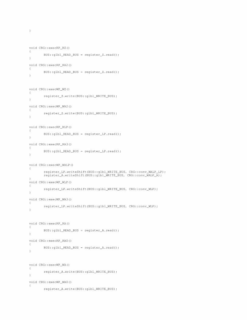
}
void CRG::execRP_RZ(){
BUS::glbl_READ_BUS = register_Z.read();}
void CRG::execRP_RA2(){
BUS::glbl_READ_BUS = register_Z.read();}
void CRG::execWP_WZ(){
register_Z.write(BUS::glbl_WRITE_BUS);}
void CRG::execWP_WA2(){
register_Z.write(BUS::glbl_WRITE_BUS);}
void CRG::execRP_RLP(){
BUS::glbl_READ_BUS = register_LP.read();}
void CRG::execRP_RA3(){
BUS::glbl_READ_BUS = register_LP.read();}
void CRG::execWP_WALP(){
register_LP.writeShift(BUS::glbl_WRITE_BUS, CRG::conv_WALP_LP);register_A.writeShift(BUS::glbl_WRITE_BUS, CRG::conv_WALP_A);
}void CRG::execWP_WLP(){
register_LP.writeShift(BUS::glbl_WRITE_BUS, CRG::conv_WLP);}
void CRG::execWP_WA3(){
register_LP.writeShift(BUS::glbl_WRITE_BUS, CRG::conv_WLP);}
void CRG::execRP_RA(){
BUS::glbl_READ_BUS = register_A.read();}
void CRG::execRP_RA0(){
BUS::glbl_READ_BUS = register_A.read();}
void CRG::execWP_WA(){
register_A.write(BUS::glbl_WRITE_BUS);}
void CRG::execWP_WA0(){
register_A.write(BUS::glbl_WRITE_BUS);

}

CTR (CTR.h)
/**************************************************************************** * CTR - INVOLUNTARY PRIORITY COUNTER subsystem * * AUTHOR: John Pultorak * DATE: 10/25/02 * FILE: CTR.h * * VERSIONS: * * DESCRIPTION: * Involuntary Counters for the Block 1 Apollo Guidance Computer prototype (AGC4). * * SOURCES: * Mostly based on information from "Logical Description for the Apollo * Guidance Computer (AGC4)", Albert Hopkins, Ramon Alonso, and Hugh * Blair-Smith, R-393, MIT Instrumentation Laboratory, 1963. * * NOTES: * ***************************************************************************** */#ifndef CTR_H#define CTR_H
#include "reg.h"
enum ctrNumber { // indexes for priority cellsOVCTR =0,
TIME2 =1, // Block II puts TIME2 firstTIME1 =2,TIME3 =3,TIME4 =4,
};
enum ctrAddr { // octal addresses of counters// Note: In Block 1, TIME1 preceeds TIME2. In Block II,// this is reversed: TIME2 preceeds TIME1. This reversal// was done so that the most significant time word occurs// at the lower address in the 2 word AGC clock. Therefore,// a common AGC software routine can be used to read the// time.
OVCTR_ADDR =0034,
TIME2_ADDR =0035, // Block II puts TIME2 firstTIME1_ADDR =0036,TIME3_ADDR =0037,TIME4_ADDR =0040,
SPARE1_ADDR =0041,
SPARE2_ADDR =0042,SPARE3_ADDR =0043
};
enum pCntrType {NOPSEL =0, // NO COUNTERPINCSEL =1, // PINCMINCSEL =2 // MINC
};
class regUpCELL : public reg { public:
// Bit synchronize the counter inputs.regUpCELL() : reg(8, "%03o") { }
};
class regDnCELL : public reg { public:

// Bit synchronize the counter inputs.regDnCELL() : reg(8, "%03o") { }
};
class CTR{public:
static void execWP_GENRST();static void execWP_WPCTR();static void execRP_RSCT();static void execWP_WOVR();static void execWP_WOVC();
static unsigned getSubseq();
static unsigned pcUp[];static unsigned pcDn[];
static regUpCELL register_UpCELL; // latches the selected priority counter cell (0-7)static regDnCELL register_DnCELL; // latches the selected priority counter cell (0-7)
private:static void resetAllpc();
};
#endif

CTR (CTR.cpp)
/**************************************************************************** * CTR - INVOLUNTARY PRIORITY COUNTER subsystem * * AUTHOR: John Pultorak * DATE: 10/25/02 * FILE: CTR.cpp * * NOTES: see header file. * ***************************************************************************** */#include "CTR.h"#include "INT.h"#include "BUS.h"#include "SEQ.h"
regUpCELL CTR::register_UpCELL; // latches the selected priority counter cell (0-7 (decimal))regDnCELL CTR::register_DnCELL; // latches the selected priority counter cell (0-7 (decimal))
unsigned CTR::pcUp[8];unsigned CTR::pcDn[8];
// PRIORITY COUNTERS
// ****************************************************// The interrupt priorities are stored in RPCELL as 1-5, but// the priority counter priorities are stored as 0-7; this// inconsistency should be fixed, probably. Also, the method// of address determination for the priority counters needs work
void CTR::resetAllpc(){
for(int i=0; i<8; i++) { pcUp[i]=0; pcDn[i]=0; }}
// priority encoder; outputs 0-7; 0=highest priority (OVCTR), 1=TIME2, 2=TIME1, etcstatic bool newPriority = true; // a simulator performance optimization; not in the hardware AGCunsigned getPriority(){
// simulator optimization; don't recompute priority if the priority inputs haven'tchanged
static unsigned priority = 7; // default (lowest priority)if(!newPriority) return priority;
priority = 7; // default (lowest priority)for(int i=0; i<8; i++) {
if(CTR::register_UpCELL.readField(i+1,i+1) |CTR::register_DnCELL.readField(i+1,i+1))
{priority = i;break;
}}newPriority = false;return priority;
}
unsigned CTR::getSubseq(){
unsigned pc = getPriority();
unsigned upCell = CTR::register_UpCELL.readField(pc+1,pc+1);unsigned dnCell = CTR::register_DnCELL.readField(pc+1,pc+1);

if(upCell == 1 && dnCell == 0)return PINCSEL;
else if(upCell == 0 && dnCell == 1) return MINCSEL;
else return NOPSEL;
}
void CTR::execWP_GENRST(){
register_UpCELL.write(0);register_DnCELL.write(0);
resetAllpc();}
void CTR::execWP_WPCTR(){
// transfer cell data into up and down synch registers
for(int i=0; i<8; i++) {
register_UpCELL.writeField(i+1,i+1,pcUp[i]);register_DnCELL.writeField(i+1,i+1,pcDn[i]);
}newPriority=true; // a simulator performance optimization; not in hardware AGC
}
// Selected counter address is requested at TP1.// Counter address is latched at TP12
void CTR::execRP_RSCT(){
BUS::glbl_READ_BUS = 034 + getPriority();}
void CTR::execWP_WOVR(){
unsigned pc = getPriority();if(register_UpCELL.readField(pc+1,pc+1)){
pcUp[pc]=0;}if(register_DnCELL.readField(pc+1,pc+1)){
pcDn[pc]=0;}
// generate various actions in response to counter overflows:switch(BUS::testOverflow(BUS::glbl_WRITE_BUS)){
case POS_OVF: // positive overflowswitch(getPriority()) // get the counter{case TIME1: CTR::pcUp[TIME2]=1; break; // overflow from TIME1 increments
TIME2case TIME3: INT::rupt[T3RUPT]=1; break; // overflow from TIME3 triggers
T3RUPTcase TIME4: INT::rupt[DSRUPT]=1; break; // overflow from TIME4 triggers
DSRUPT}break;
case NEG_OVF: break; // no actions for negative counter overflow}
}
void CTR::execWP_WOVC(){

switch(BUS::testOverflow(BUS::glbl_WRITE_BUS)){
case POS_OVF: CTR::pcUp[OVCTR]=1; break; // incr OVCTR (034)case NEG_OVF: CTR::pcDn[OVCTR]=1; break; // decr OVCTR (034)
}
}
// register_PCELL: Overflow from the selected counter appears// on the bus when WOVR or WOVC is asserted;// it could be used to trigger an interrupt// or routed to increment another counter

DSP (DSP.h)
/**************************************************************************** * DSP - DSKY DISPLAY subsystem * * AUTHOR: John Pultorak * DATE: 9/22/01 * FILE: DSP.h * * VERSIONS: * * DESCRIPTION: * DSKY Display for the Block 1 Apollo Guidance Computer prototype (AGC4). * * SOURCES: * Mostly based on information from "Logical Description for the Apollo * Guidance Computer (AGC4)", Albert Hopkins, Ramon Alonso, and Hugh * Blair-Smith, R-393, MIT Instrumentation Laboratory, 1963. * * NOTES: * ***************************************************************************** */#ifndef DSP_H#define DSP_H
class DSP{public:
// DSKY display
// major mode displaystatic char MD1;static char MD2;
// verb displaystatic char VD1;static char VD2;
// noun displaystatic char ND1;static char ND2;
// R1static char R1S;static char R1D1;static char R1D2;static char R1D3;static char R1D4;static char R1D5;
// R2static char R2S;static char R2D1;static char R2D2;static char R2D3;static char R2D4;static char R2D5;
// R3static char R3S;static char R3D1;static char R3D2;static char R3D3;static char R3D4;static char R3D5;
// These flags control the sign; if both bits are 0 or 1, there is no sign.// Otherwise, the sign is set by the selected bit.
static unsigned R1SP;static unsigned R1SM;static unsigned R2SP;static unsigned R2SM;static unsigned R3SP;static unsigned R3SM;

// verb/noun flashstatic unsigned flash;
static void clearOut0();
static char signConv(unsigned p, unsigned m);
static char outConv(unsigned in);
static void decodeRelayWord(unsigned in);};
#endif

DSP (DSP.cpp)
/**************************************************************************** * DSP - DSKY DISPLAY subsystem * * AUTHOR: John Pultorak * DATE: 9/22/01 * FILE: DSP.cpp * * NOTES: see header file. * ***************************************************************************** */#include "DSP.h"#include <string.h>#include <iostream.h>#include <stdio.h>
bool dskyChanged = false; // true when DSKY display changes
// major mode displaychar DSP::MD1=0;char DSP::MD2=0;
// verb displaychar DSP::VD1=0;char DSP::VD2=0;
// noun displaychar DSP::ND1=0;char DSP::ND2=0;
// R1char DSP::R1S=0;char DSP::R1D1=0;char DSP::R1D2=0;char DSP::R1D3=0;char DSP::R1D4=0;char DSP::R1D5=0;
// R2char DSP::R2S=0;char DSP::R2D1=0;char DSP::R2D2=0;char DSP::R2D3=0;char DSP::R2D4=0;char DSP::R2D5=0;
// R3char DSP::R3S=0;char DSP::R3D1=0;char DSP::R3D2=0;char DSP::R3D3=0;char DSP::R3D4=0;char DSP::R3D5=0;
// These flags control the sign; if both bits are 0 or 1, there is no sign.// Otherwise, the sign is set by the selected bit.
unsigned DSP::R1SP=0;unsigned DSP::R1SM=0;unsigned DSP::R2SP=0;unsigned DSP::R2SM=0;unsigned DSP::R3SP=0;unsigned DSP::R3SM=0;
// flag controls 1 Hz flash of verb and noun displayunsigned DSP::flash = 0; // 0=flash off, 1=flash on
void DSP::clearOut0(){
MD1 = MD2 = ' '; // major mode displayVD1 = VD2 = ' '; // verb display

ND1 = ND2 = ' '; // noun displayR1S = R1D1 = R1D2 = R1D3 = R1D4 = R1D5 = ' '; // R1R2S = R2D1 = R2D2 = R2D3 = R2D4 = R2D5 = ' '; // R2R3S = R3D1 = R3D2 = R3D3 = R3D4 = R3D5 = ' '; // R3
R1SP = R1SM = 0;R2SP = R2SM = 0;R3SP = R3SM = 0;
}
char DSP::signConv(unsigned p, unsigned m){
if(p && !m)return '+';
else if(m && !p)return '-';
elsereturn ' ';
}
char DSP::outConv(unsigned in){
switch(in){case 000: return ' ';case 025: return '0';case 003: return '1';case 031: return '2';case 033: return '3';case 017: return '4';case 036: return '5';case 034: return '6';case 023: return '7';case 035: return '8';case 037: return '9';}return ' '; // error
}
void DSP::decodeRelayWord(unsigned in){
unsigned charSelect = (in & 074000) >> 11; // get bits 15-12unsigned b11 = (in & 02000) >> 10; // get bit 11unsigned bHigh = (in & 01740) >> 5; // get bits 10-6unsigned bLow = in & 037;
//******************************#ifdef NOTDEF
char buf[80]; sprintf(buf, "bits15-12: %02o, Bit11: %01o, bits10-6: %02o, bits5-1: %02o",
charSelect, b11, bHigh, bLow);cout << buf << endl;
#endifdskyChanged = true;//******************************
switch(charSelect){case 013: MD1 = outConv(bHigh); MD2 = outConv(bLow); break;case 012: VD1 = outConv(bHigh); VD2 = outConv(bLow); flash = b11; break;case 011: ND1 = outConv(bHigh); ND2 = outConv(bLow); break;case 010: R1D1 = outConv(bLow); break;// UPACT not implemented
case 007: R1SP = b11; R1S = signConv(R1SP, R1SM);R1D2 = outConv(bHigh);R1D3 = outConv(bLow); break;
case 006: R1SM = b11; R1S = signConv(R1SP, R1SM);R1D4 = outConv(bHigh);R1D5 = outConv(bLow); break;
case 005: R2SP = b11; R2S = signConv(R2SP, R2SM);R2D1 = outConv(bHigh);R2D2 = outConv(bLow); break;
case 004: R2SM = b11; R2S = signConv(R2SP, R2SM);R2D3 = outConv(bHigh);R2D4 = outConv(bLow); break;
case 003: R2D5 = outConv(bHigh);R3D1 = outConv(bLow); break;
case 002: R3SP = b11; R3S = signConv(R3SP, R3SM);R3D2 = outConv(bHigh);R3D3 = outConv(bLow); break;
case 001: R3SM = b11; R3S = signConv(R3SP, R3SM);R3D4 = outConv(bHigh);R3D5 = outConv(bLow); break;
}}

INP (INP.h)
/**************************************************************************** * INP - INPUT REGISTER subsystem * * AUTHOR: John Pultorak * DATE: 9/22/01 * FILE: INP.h * * VERSIONS: * * DESCRIPTION: * Input Registers for the Block 1 Apollo Guidance Computer prototype (AGC4). * * SOURCES: * Mostly based on information from "Logical Description for the Apollo * Guidance Computer (AGC4)", Albert Hopkins, Ramon Alonso, and Hugh * Blair-Smith, R-393, MIT Instrumentation Laboratory, 1963. * * NOTES: * ***************************************************************************** */#ifndef INP_H#define INP_H
#include "reg.h"
class regIn0 : public reg { public:
regIn0() : reg(16, "%06o") { }};
class regIn1 : public reg { public:
regIn1() : reg(16, "%06o") { }};
class regIn2 : public reg { public:
regIn2() : reg(16, "%06o") { }};
class regIn3 : public reg { public:
regIn3() : reg(16, "%06o") { }};
class INP{public:
static void execRP_RA4();static void execRP_RA5();static void execRP_RA6();static void execRP_RA7();static regIn0 register_IN0; // input register 0static regIn1 register_IN1; // input register 1static regIn2 register_IN2; // input register 2static regIn3 register_IN3; // input register 3
};
#endif
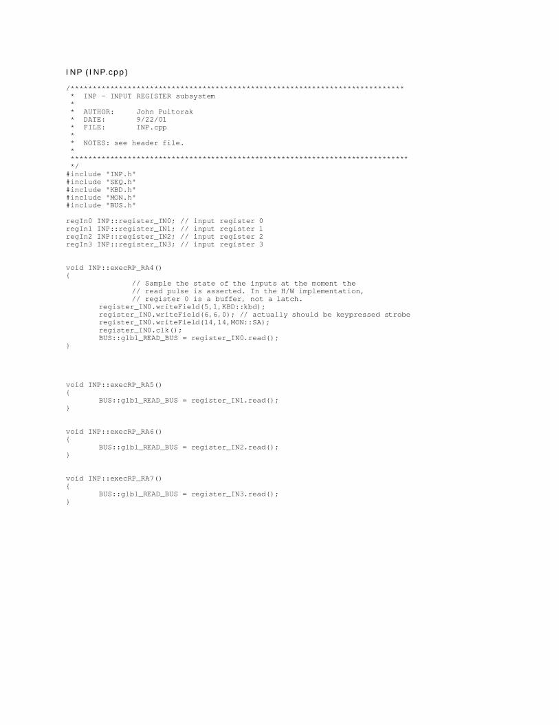
INP (INP.cpp)
/**************************************************************************** * INP - INPUT REGISTER subsystem * * AUTHOR: John Pultorak * DATE: 9/22/01 * FILE: INP.cpp * * NOTES: see header file. * ***************************************************************************** */#include "INP.h"#include "SEQ.h"#include "KBD.h"#include "MON.h"#include "BUS.h"
regIn0 INP::register_IN0; // input register 0regIn1 INP::register_IN1; // input register 1regIn2 INP::register_IN2; // input register 2regIn3 INP::register_IN3; // input register 3
void INP::execRP_RA4(){
// Sample the state of the inputs at the moment the// read pulse is asserted. In the H/W implementation,// register 0 is a buffer, not a latch.
register_IN0.writeField(5,1,KBD::kbd);register_IN0.writeField(6,6,0); // actually should be keypressed stroberegister_IN0.writeField(14,14,MON::SA);register_IN0.clk();BUS::glbl_READ_BUS = register_IN0.read();
}
void INP::execRP_RA5(){
BUS::glbl_READ_BUS = register_IN1.read();}
void INP::execRP_RA6(){
BUS::glbl_READ_BUS = register_IN2.read();}
void INP::execRP_RA7(){
BUS::glbl_READ_BUS = register_IN3.read();}

INT (INT.h)
/**************************************************************************** * INT - PRIORITY INTERRUPT subsystem * * AUTHOR: John Pultorak * DATE: 9/22/01 * FILE: INT.h * * VERSIONS: * * DESCRIPTION: * Priority Interrupts for the Block 1 Apollo Guidance Computer prototype (AGC4). * * SOURCES: * Mostly based on information from "Logical Description for the Apollo * Guidance Computer (AGC4)", Albert Hopkins, Ramon Alonso, and Hugh * Blair-Smith, R-393, MIT Instrumentation Laboratory, 1963. * * NOTES: * ***************************************************************************** */#ifndef INT_H#define INT_H
#include "reg.h"
enum ruptAddress {// Addresses for service routines of vectored interrupts
T3RUPT_ADDR =02004, // option 1: overflow of TIME 3ERRUPT_ADDR =02010, // option 2: error signalDSRUPT_ADDR =02014, // option 3: telemetry end pulse or TIME 4 overflowKEYRUPT_ADDR =02020, // option 4: activity from MARK, keyboard, or tape reader
};
enum ruptNumber {// Option number (selects rupt priority cell)// NOTE: the priority cells (rupt[]) are indexed 0-4, but stored in the // RPCELL register as 1-5; (0 in RPCELL means no interrupt)
T3RUPT =0, // option 1: overflow of TIME 3ERRUPT =1, // option 2: error signalDSRUPT =2, // option 3: telemetry end pulse or TIME 4 overflowKEYRUPT =3, // option 4: activity from MARK, keyboard, or tape reader
};
class regRPCELL : public reg { public:
regRPCELL() : reg(5, "%02o") { }};// also inhibits additional interrupts while an interrupt is being processed
class regINHINT1 : public reg { public:
regINHINT1() : reg(1, "%01o") { }};
class regINHINT : public reg { public:
regINHINT() : reg(1, "%01o") { }};
class INT{public:
friend class CLK;friend class MON;
static void execRP_RRPA();
static void execWP_GENRST();static void execWP_RPT();static void execWP_KRPT();static void execWP_CLRP();static void execWP_WOVI();static void execWP_CLINH1();static void execWP_INH();static void execWP_CLINH();
static bool IRQ(); // returns true if an interrupt is requested
static unsigned rupt[];
private:static void resetAllRupt();static unsigned getPriorityRupt();
static regRPCELL register_RPCELL; // latches the selected priority interrupt vector (1-5)static regINHINT1 register_INHINT1; // inhibits interrupts for 1 instruction (on WOVI)static regINHINT register_INHINT; // inhibits interrupts on INHINT, reenables on RELINT
};
#endif

INT (INT.cpp)
/**************************************************************************** * INT - PRIORITY INTERRUPT subsystem * * AUTHOR: John Pultorak * DATE: 9/22/01 * FILE: INT.cpp * * NOTES: see header file. * ***************************************************************************** */#include "INT.h"#include "SEQ.h"#include "BUS.h"
regRPCELL INT::register_RPCELL; // latches the selected priority interrupt vector (1-5)regINHINT1 INT::register_INHINT1; // inhibits interrupts for 1 instruction (on WOVI)regINHINT INT::register_INHINT; // inhibits interrupts on INHINT, reenables on RELINT
// NOTE: the priority cells (rupt[]) are indexed 0-4, but stored in the // RPCELL register as 1-5; (0 in RPCELL means no interrupt)unsigned INT::rupt[5];
bool INT::IRQ(){
if( INT::getPriorityRupt() // if interruptrequested
&& INT::register_RPCELL.read() == 0 // and interrupt not currently beingserviced
&& INT::register_INHINT1.read() == 0 // and interrupt not inhibited for 1instruction
&& INT::register_INHINT.read() == 0) // and interrupts enabled (RELINT){
return true;}return false;
}
void INT::resetAllRupt(){
for(int i=0; i<5; i++) { rupt[i]=0; }}
// interrupt vector; outputs 1-5 (decimal) == vector; 0 == no interruptunsigned INT::getPriorityRupt(){
for(int i=0; i<5; i++) { if(rupt[i]) return i+1; }return 0;
}
void INT::execRP_RRPA(){
BUS::glbl_READ_BUS = 02000 + (register_RPCELL.read() << 2);}
// latches the selected priority interrupt vector (1-5)// also inhibits additional interrupts while an interrupt is being processed
void INT::execWP_GENRST(){
register_RPCELL.write(0);register_INHINT.write(1);resetAllRupt();
}
void INT::execWP_RPT(){

register_RPCELL.write(INT::getPriorityRupt());}
void INT::execWP_KRPT(){
INT::rupt[register_RPCELL.read()-1] = 0;}
void INT::execWP_CLRP(){
register_RPCELL.write(0);}
// INHINT1: inhibits interrupts for 1 instruction (on WOVI)
void INT::execWP_WOVI(){
if(BUS::testOverflow(BUS::glbl_WRITE_BUS) != NO_OVF) register_INHINT1.write(1);
}
void INT::execWP_CLINH1(){
register_INHINT1.write(0);}
// INHINT: inhibits interrupts on INHINT, reenables on RELINT
void INT::execWP_INH(){
register_INHINT.write(1);}
void INT::execWP_CLINH(){
register_INHINT.write(0);}

ISD (ISD.h)
/**************************************************************************** * ISD - INSTRUCTION SUBSEQUENCE DECODER subsystem * * AUTHOR: John Pultorak * DATE: 9/22/01 * FILE: ISD.h * * VERSIONS: * * DESCRIPTION: * Instruction Subsequence Decoder for the Block 1 Apollo Guidance Computer * prototype (AGC4). * * SOURCES: * Mostly based on information from "Logical Description for the Apollo * Guidance Computer (AGC4)", Albert Hopkins, Ramon Alonso, and Hugh * Blair-Smith, R-393, MIT Instrumentation Laboratory, 1963. * * NOTES: * ***************************************************************************** */#ifndef ISD_H#define ISD_H
#include "SEQ.h"#include "CTR.h"
// INSTRUCTION SUBSEQUENCE DECODER
#ifdef NOTDEFclass ISD{public:
static subseq instructionSubsequenceDecoder();
static char* ISD::subseqString[];};#endif
#endif

ISD (ISD.cpp)
/**************************************************************************** * ISD - INSTRUCTION SUBSEQUENCE DECODER subsystem * * AUTHOR: John Pultorak * DATE: 9/22/01 * FILE: ISD.cpp * * NOTES: see header file. * ***************************************************************************** */#include "ISD.h"
#ifdef NOTDEFchar* ISD::subseqString[] ={
"TC0","CCS0","CCS1","NDX0","NDX1","RSM3","XCH0","CS0","TS0","AD0","MASK0","MP0","MP1","MP3","DV0","DV1","SU0","RUPT1","RUPT3","STD2","PINC0","MINC0","SHINC0","NO_SEQ"
};
subseq ISD::instructionSubsequenceDecoder(){
// Combinational logic decodes instruction and the stage count // to get the instruction subsequence.
static subseq decode[16][4] = {{ TC0, RUPT1, STD2, RUPT3 }, // 00{ CCS0, CCS1, NO_SEQ, NO_SEQ }, // 01{ NDX0, NDX1, NO_SEQ, RSM3 }, // 02{ XCH0, NO_SEQ, STD2, NO_SEQ }, // 03
{ NO_SEQ, NO_SEQ, NO_SEQ, NO_SEQ }, // 04{ NO_SEQ, NO_SEQ, NO_SEQ, NO_SEQ }, // 05{ NO_SEQ, NO_SEQ, NO_SEQ, NO_SEQ }, // 06{ NO_SEQ, NO_SEQ, NO_SEQ, NO_SEQ }, // 07{ NO_SEQ, NO_SEQ, NO_SEQ, NO_SEQ }, // 10
{ MP0, MP1, NO_SEQ, MP3 }, // 11{ DV0, DV1, STD2, NO_SEQ }, // 12{ SU0, NO_SEQ, STD2, NO_SEQ }, // 13
{ CS0, NO_SEQ, STD2, NO_SEQ }, // 14{ TS0, NO_SEQ, STD2, NO_SEQ }, // 15{ AD0, NO_SEQ, STD2, NO_SEQ }, // 16{ MASK0, NO_SEQ, STD2, NO_SEQ } // 17
};
switch(CTR::getSubseq()){case PINCSEL: return PINC0;
case MINCSEL: return MINC0;default: return decode[SEQ::register_SQ.read()][SEQ::register_STB.read()];}
}
#endif

KBD (KBD.h)
/**************************************************************************** * KBD - DSKY KEYBOARD subsystem * * AUTHOR: John Pultorak * DATE: 9/22/01 * FILE: KBD.h * * VERSIONS: * * DESCRIPTION: * DSKY Keyboard for the Block 1 Apollo Guidance Computer prototype (AGC4). * * SOURCES: * Mostly based on information from "Logical Description for the Apollo * Guidance Computer (AGC4)", Albert Hopkins, Ramon Alonso, and Hugh * Blair-Smith, R-393, MIT Instrumentation Laboratory, 1963. * * NOTES: * ***************************************************************************** */#ifndef KBD_H#define KBD_H
enum keyInType {// DSKY keyboard input codes: Taken from E-1574, Appendix 1// These codes enter the computer through bits 1-5 of IN0.// The MSB is in bit 5; LSB in bit 1. Key entry generates KEYRUPT.KEYIN_NONE =0, // no key depressed**KEYIN_0 =020,KEYIN_1 =001,KEYIN_2 =002,KEYIN_3 =003,KEYIN_4 =004,KEYIN_5 =005,KEYIN_6 =006,KEYIN_7 =007,KEYIN_8 =010,KEYIN_9 =011,KEYIN_VERB =021,KEYIN_ERROR_RESET =022,KEYIN_KEY_RELEASE =031,KEYIN_PLUS =032,KEYIN_MINUS =033,KEYIN_ENTER =034,KEYIN_CLEAR =036,KEYIN_NOUN =037,
};
class KBD{public:
static keyInType kbd; // latches the last key entry from the DSKYstatic void keypress(keyInType c);
};
#endif

KBD (KBD.cpp)
/**************************************************************************** * KBD - DSKY KEYBOARD subsystem * * AUTHOR: John Pultorak * DATE: 9/22/01 * FILE: KBD.cpp * * NOTES: see header file. * ***************************************************************************** */#include "KBD.h"#include "INT.h"
// DSKY keyboardkeyInType KBD::kbd=KEYIN_NONE; // latches the last key entry from the DSKY
void KBD::keypress(keyInType c){
// latch the keycodekbd = c;
// generate KEYRUPT interruptINT::rupt[KEYRUPT] = 1;
}

MBF (MBF.h)
/**************************************************************************** * MBF - MEMORY BUFFER REGISTER subsystem * * AUTHOR: John Pultorak * DATE: 9/22/01 * FILE: MBF.h * * VERSIONS: * * DESCRIPTION: * Memory Buffer Register for the Block 1 Apollo Guidance Computer prototype (AGC4). * * SOURCES: * Mostly based on information from "Logical Description for the Apollo * Guidance Computer (AGC4)", Albert Hopkins, Ramon Alonso, and Hugh * Blair-Smith, R-393, MIT Instrumentation Laboratory, 1963. * * NOTES: * ***************************************************************************** */#ifndef MBF_H#define MBF_H
#include "reg.h"
class regG : public reg { public:
// all memory bits except bit 15 (parity)// bit 15 is not used, so ignore it.
regG() : reg(16, "%06o") { }};
class MBF{public:
static void execWP_GENRST();
static void execRP_RG();static void execRP_WE();
static void execWP_WGn();static void execWP_WGx();static void execWP_W20();static void execWP_W21();static void execWP_W22();static void execWP_W23();static void execWP_SBWG();
// Bit 15 (parity) is kept in a separate register in PAR// because it is independently loaded.
static regG register_G; // memory buffer register (except for bit 15)
static unsigned conv_RG[];static unsigned conv_WGn[];static unsigned conv_W20[];static unsigned conv_W21[];static unsigned conv_W22[];static unsigned conv_W23[];static unsigned conv_SBWG[];static unsigned conv_WE[];
};
#endif

MBF (MBF.cpp)
/**************************************************************************** * MBF - MEMORY BUFFER REGISTER subsystem * * AUTHOR: John Pultorak * DATE: 9/22/01 * FILE: MBF.cpp * * NOTES: see header file. * ***************************************************************************** */#include "MBF.h"#include "SEQ.h"#include "ADR.h"#include "BUS.h"#include "PAR.h"#include "MEM.h"
// The actual bit 15 of register_G is not used.regG MBF::register_G; // memory buffer register (except bit 15: parity)
unsigned MBF::conv_RG[] ={ SG, SG, B14, B13, B12, B11, B10, B9, B8, B7, B6, B5, B4, B3, B2, B1 };
unsigned MBF::conv_SBWG[] ={ SGM, BX, B14, B13, B12, B11, B10, B9, B8, B7, B6, B5, B4, B3, B2, B1 };
unsigned MBF::conv_WE[] ={ BX, SG, B14, B13, B12, B11, B10, B9, B8, B7, B6, B5, B4, B3, B2, B1 };
unsigned MBF::conv_W20[] ={ B1, BX, SG, B14, B13, B12, B11, B10, B9, B8, B7, B6, B5, B4, B3, B2 };
unsigned MBF::conv_W21[] ={ SG, BX, SG, B14, B13, B12, B11, B10, B9, B8, B7, B6, B5, B4, B3, B2 };
unsigned MBF::conv_W22[] ={ B14, BX, B13, B12, B11, B10, B9, B8, B7, B6, B5, B4, B3, B2, B1, SG };
unsigned MBF::conv_W23[] ={ SG, BX, B13, B12, B11, B10, B9, B8, B7, B6, B5, B4, B3, B2, B1, SG };
void MBF::execWP_GENRST(){
register_G.write(0);}
void MBF::execRP_RG(){
if(ADR::GTR_17()){
BUS::glbl_READ_BUS = register_G.shiftData(0, register_G.read(), MBF::conv_RG); }
}
void MBF::execRP_WE(){
// Write G into memory; shift the sign to bit 15; parity is written from the // PAR subsystem
MEM::MEM_DATA_BUS = (register_G.shiftData(0, MBF::register_G.read(), MBF::conv_WE));}

void MBF::execWP_WGn(){
register_G.write(BUS::glbl_WRITE_BUS);}
void MBF::execWP_WGx(){
// This is only used in PINC, MINC, and SHINC. Does not clear G// register; writes (ORs) into G from RWBus and writes into parity// from 1-15 generator. The sequence calls CLG in a previous TP to// reset G to zero, so the OR operation can be safely eliminated// from my implementation of the design.
register_G.write(BUS::glbl_WRITE_BUS);}
void MBF::execWP_W20(){
register_G.writeShift(BUS::glbl_WRITE_BUS, MBF::conv_W20);}
void MBF::execWP_W21(){
register_G.writeShift(BUS::glbl_WRITE_BUS, MBF::conv_W21);}
void MBF::execWP_W22(){
register_G.writeShift(BUS::glbl_WRITE_BUS, MBF::conv_W22);}
void MBF::execWP_W23(){
register_G.writeShift(BUS::glbl_WRITE_BUS, MBF::conv_W23);}
void MBF::execWP_SBWG(){
register_G.writeShift(MEM::MEM_DATA_BUS, MBF::conv_SBWG);
}
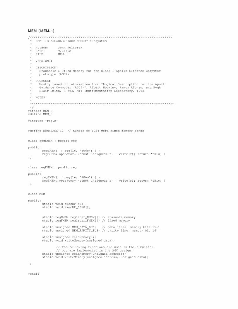
MEM (MEM.h)
/**************************************************************************** * MEM - ERASEABLE/FIXED MEMORY subsystem * * AUTHOR: John Pultorak * DATE: 9/26/02 * FILE: MEM.h * * VERSIONS: * * DESCRIPTION: * Eraseable & Fixed Memory for the Block 1 Apollo Guidance Computer * prototype (AGC4). * * SOURCES: * Mostly based on information from "Logical Description for the Apollo * Guidance Computer (AGC4)", Albert Hopkins, Ramon Alonso, and Hugh * Blair-Smith, R-393, MIT Instrumentation Laboratory, 1963. * * NOTES: * ***************************************************************************** */#ifndef MEM_H#define MEM_H
#include "reg.h"
#define NUMFBANK 12 // number of 1024 word fixed memory banks
class regEMEM : public reg { public:
regEMEM() : reg(16, "%06o") { }regEMEM& operator= (const unsigned& r) { write(r); return *this; }
};
class regFMEM : public reg { public:
regFMEM() : reg(16, "%06o") { }regFMEM& operator= (const unsigned& r) { write(r); return *this; }
};
class MEM{public:
static void execWP_WE();static void execRP_SBWG();
static regEMEM register_EMEM[]; // erasable memorystatic regFMEM register_FMEM[]; // fixed memory
static unsigned MEM_DATA_BUS; // data lines: memory bits 15-1static unsigned MEM_PARITY_BUS; // parity line: memory bit 16
static unsigned readMemory();static void writeMemory(unsigned data);
// The following functions are used in the simulator,// but are implemented in the AGC design.
static unsigned readMemory(unsigned address);static void writeMemory(unsigned address, unsigned data);
};
#endif

MEM (MEM.cpp)
/**************************************************************************** * MEM - ERASEABLE/FIXED MEMORY subsystem * * AUTHOR: John Pultorak * DATE: 9/26/02 * FILE: MEM.cpp * * NOTES: see header file. * ***************************************************************************** */#include "MEM.h"#include "ADR.h"#include "stdlib.h"
regEMEM MEM::register_EMEM[1024]; // erasable memoryregFMEM MEM::register_FMEM[1024*(NUMFBANK+1)]; // fixed memory (lowest 1024 words ignored)
unsigned MEM::MEM_DATA_BUS = 0; // data lines: memory bits 15-1unsigned MEM::MEM_PARITY_BUS = 0; // parity line: memory bit 16
void MEM::execWP_WE(){
// Write into memory; parity bit in bit 16writeMemory( (MEM_PARITY_BUS << 15) | MEM_DATA_BUS );
}
void MEM::execRP_SBWG(){
MEM_DATA_BUS = readMemory() & 0077777; // everything except parityMEM_PARITY_BUS = (readMemory() & 0100000) >> 15; // parity bit only
}
unsigned MEM::readMemory(){
// Return memory value addressed by lower 10 bits of the S register (1K) and the// bank decoder (which selects the 1K bank)
unsigned lowAddress = ADR::register_S.readField(10,1);
if(ADR::bankDecoder() == 0)return MEM::register_EMEM[lowAddress].read();
unsigned highAddress = ADR::bankDecoder() << 10;return MEM::register_FMEM[highAddress | lowAddress].read();
}
void MEM::writeMemory(unsigned data){
// Write into erasable memory addressed by lower 10 bits of the S register (1K) // and the bank decoder (which selects the 1K bank)
unsigned lowAddress = ADR::register_S.readField(10,1);if(ADR::bankDecoder() == 0){
MEM::register_EMEM[lowAddress].write(data);MEM::register_EMEM[lowAddress].clk(); // not a synchronous FF, so execute
immediately *************}
}
unsigned MEM::readMemory(unsigned address){
// Address is 14 bits. This function is used by the simulator for examining// memory; it is not part of the AGC design.
unsigned lowAddress = address & 01777;unsigned bank = (address & 036000) >> 10;
if(bank == 0)return MEM::register_EMEM[lowAddress].read();
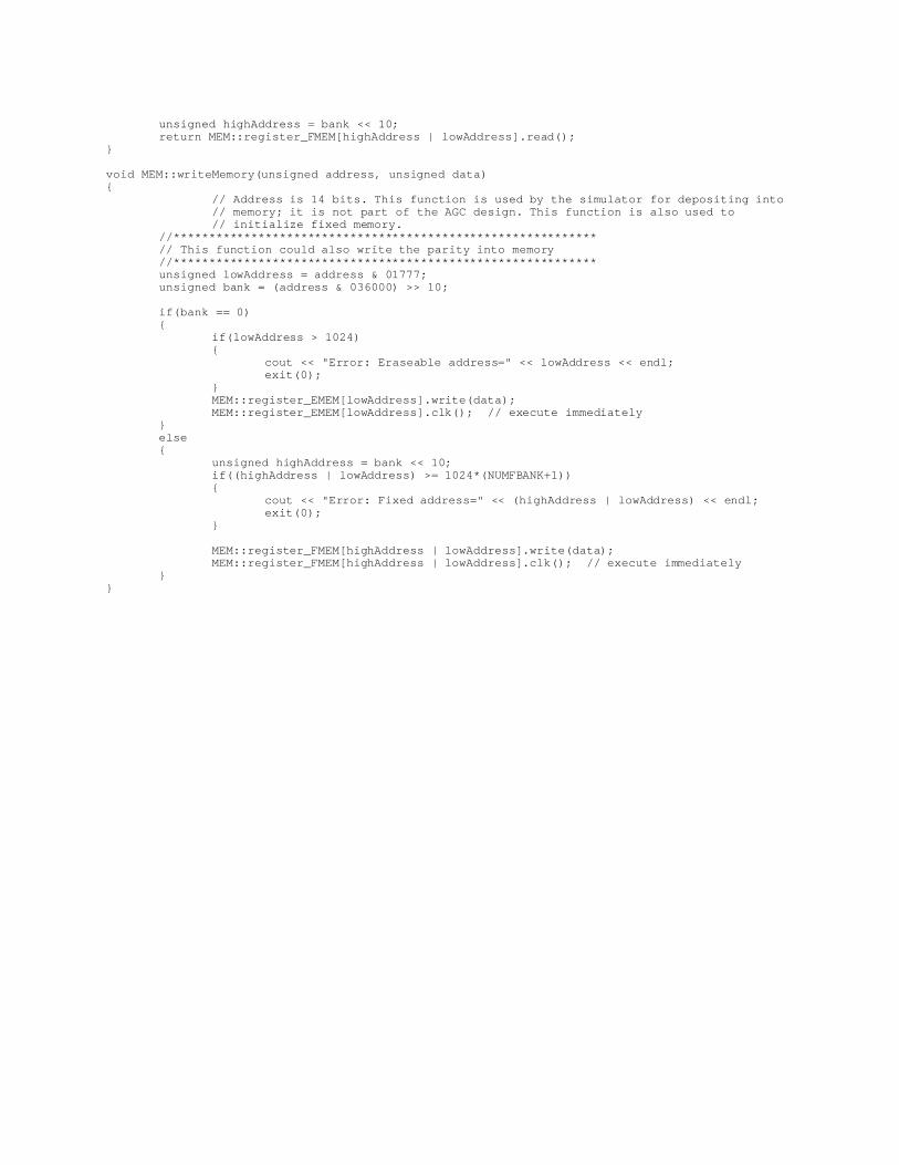
unsigned highAddress = bank << 10;return MEM::register_FMEM[highAddress | lowAddress].read();
}
void MEM::writeMemory(unsigned address, unsigned data){
// Address is 14 bits. This function is used by the simulator for depositing into// memory; it is not part of the AGC design. This function is also used to// initialize fixed memory.
//************************************************************// This function could also write the parity into memory//************************************************************unsigned lowAddress = address & 01777;unsigned bank = (address & 036000) >> 10;
if(bank == 0){
if(lowAddress > 1024) {
cout << "Error: Eraseable address=" << lowAddress << endl; exit(0);
}MEM::register_EMEM[lowAddress].write(data);MEM::register_EMEM[lowAddress].clk(); // execute immediately
}else{
unsigned highAddress = bank << 10;if((highAddress | lowAddress) >= 1024*(NUMFBANK+1)) {
cout << "Error: Fixed address=" << (highAddress | lowAddress) << endl; exit(0);
}
MEM::register_FMEM[highAddress | lowAddress].write(data);MEM::register_FMEM[highAddress | lowAddress].clk(); // execute immediately
}}

MON (MON.h)
/**************************************************************************** * MON - AGC MONITOR subsystem * * AUTHOR: John Pultorak * DATE: 9/22/01 * FILE: MON.h * * VERSIONS: * * DESCRIPTION: * AGC Monitor for the Block 1 Apollo Guidance Computer prototype (AGC4). * * SOURCES: * Mostly based on information from "Logical Description for the Apollo * Guidance Computer (AGC4)", Albert Hopkins, Ramon Alonso, and Hugh * Blair-Smith, R-393, MIT Instrumentation Laboratory, 1963. * * NOTES: * ***************************************************************************** */#ifndef MON_H#define MON_H
class MON{public:
static void displayAGC();
static char* MON::clkTypestring[];
static unsigned PURST; // power up resetstatic unsigned RUN; // run/halt switchstatic unsigned STEP; // single step switchstatic unsigned INST; // instruction/sequence step select switchstatic unsigned FCLK; // clock mode (0=single (manual) clock, 1=continuous clock)
static unsigned SA; // "standby allowed" SW; // 0=NO (full power), 1=YES (low power)
static unsigned SCL_ENAB; // "scaler enabled" SW; 0=NO (scaler halted), 1=YES(scaler running)
};
#endif

MON (MON.cpp)
/**************************************************************************** * MON - AGC MONITOR subsystem * * AUTHOR: John Pultorak * DATE: 9/22/01 * FILE: MON.cpp * * NOTES: see header file. * ***************************************************************************** */#include "MON.h"
#include "TPG.h"#include "MON.h"#include "SCL.h"#include "SEQ.h"#include "INP.h"#include "OUT.h"#include "BUS.h"#include "DSP.h"#include "ADR.h"#include "PAR.h"#include "MBF.h"#include "MEM.h"#include "CTR.h"#include "INT.h"#include "KBD.h"#include "CRG.h"#include "ALU.h"#include "CPM.h"#include "ISD.h"#include "CLK.h"
unsigned MON::PURST=1; // power up reset; initially high at startupunsigned MON::RUN=0; // run/halt switchunsigned MON::STEP=0; // single step switchunsigned MON::INST=1; // instruction/sequence step select switchunsigned MON::FCLK=0; // clock mode
unsigned MON::SA=0; // "standby allowed" SW; 0=NO (full power), 1=YES (low power)
unsigned MON::SCL_ENAB=1; // "scaler enabled" SW; 0=NO (scaler halted), 1=YES (scalerrunning)
void MON::displayAGC(){
char buf[100];cout << "AGC4 SIMULATOR 1.16 -------------------------------" << endl;sprintf(buf," TP: %-5s F17:%1d F13:%1d F10:%1d SCL:%06o",
TPG::tpTypestring[TPG::register_SG.read()], SCL::register_F17.read(), SCL::register_F13.read(), SCL::register_F10.read(),SCL::register_SCL.read());
cout << buf << endl;
sprintf(buf, " STA:%01o STB:%01o BR1:%01o BR2:%01o SNI:%01o CI:%01o LOOPCTR:%01o",
SEQ::register_STA.read(), SEQ::register_STB.read(), SEQ::register_BR1.read(), SEQ::register_BR2.read(),SEQ::register_SNI.read(), ALU::register_CI.read(), SEQ::register_LOOPCTR.read());
cout << buf << endl;
sprintf(buf, " RPCELL:%05o INH1:%01o INH:%01o UpCELL:%03o DnCELL:%03o SQ:%02o %-6s %-6s",
INT::register_RPCELL.read(), INT::register_INHINT1.read(),INT::register_INHINT.read(),
CTR::register_UpCELL.read(), CTR::register_DnCELL.read(),SEQ::register_SQ.read(), SEQ::instructionString[SEQ::register_SQ.read()], CPM::subseqString[SEQ::glbl_subseq]);
cout << buf << endl;
sprintf(buf, " CP:%s", SEQ::getControlPulses());cout << buf << endl;

// For the G register, bit 15 comes from register G15; the other bits (16, 14-1)come
// from register G.sprintf(buf, " S: %04o G:%06o P:%06o (r)RUN :%1d (p)PURST:%1d
(F2,F4)FCLK:%1d", ADR::register_S.read(), (MBF::register_G.read() & 0137777) | (PAR::register_G15.read() << 14), PAR::register_P.read(),MON::RUN, MON::PURST, MON::FCLK);
cout << buf << endl;
sprintf(buf, " RBU:%06o WBU:%06o P2:%01o (s)STEP:%1d", BUS::glbl_READ_BUS & 0177777, BUS::glbl_WRITE_BUS & 0177777,
PAR::register_P2.read(), MON::STEP);cout << buf << endl;
char parityAlm = ' ';if(PAR::register_PALM.read()) parityAlm = '*';
sprintf(buf, " B:%06o CADR:%06o (n)INST:%1d PALM:[%c]", ALU::register_B.read(), ADR::getEffectiveAddress(), MON::INST, parityAlm);
cout << buf << endl;
sprintf(buf, " X:%06o Y:%06o U:%06o (a)SA :%1d", ALU::register_X.read(), ALU::register_Y.read(), ALU::register_U.read(), MON::SA);
cout << buf << endl;
cout << endl;sprintf(buf, "00 A:%06o 15 BANK:%02o 36 TIME1:%06o 53 OPT Y:%06o",
CRG::register_A.read(), ADR::register_BNK.read(), MEM::readMemory(036),MEM::readMemory(053));
cout << buf << endl;sprintf(buf, "01 Q:%06o 16 RELINT:%6s 37 TIME3:%06o 54 TRKR X:%06o",
CRG::register_Q.read(),"", MEM::readMemory(037), MEM::readMemory(054));cout << buf << endl;sprintf(buf, "02 Z:%06o 17 INHINT:%6s 40 TIME4:%06o 55 TRKR Y:%06o",
CRG::register_Z.read(),"", MEM::readMemory(040), MEM::readMemory(055));cout << buf << endl;sprintf(buf, "03 LP:%06o 20 CYR:%06o 41 UPLINK:%06o 56 TRKR Z:%06o",
CRG::register_LP.read(), MEM::readMemory(020), MEM::readMemory(041),MEM::readMemory(056));
cout << buf << endl;
sprintf(buf, "04 IN0:%06o 21 SR:%06o 42 OUTCR1:%06o", INP::register_IN0.read(), MEM::readMemory(021), MEM::readMemory(042));
cout << buf << endl;
char progAlm = ' ';if(OUT::register_OUT1.read() & 0400) progAlm = '*';
char compFail = ' '; // also called 'check fail' and 'oper err'if(OUT::register_OUT1.read() & 0100) compFail = '*';
char keyRels = ' ';if(OUT::register_OUT1.read() & 020) keyRels = '*';
char upTl = ' ';if(OUT::register_OUT1.read() & 004) upTl = '*';
char comp = ' '; // also called comp actyif(OUT::register_OUT1.read() & 001) comp = '*';
sprintf(buf, "05 IN1:%06o 22 CYL:%06o 43 OUTCR2:%06o CF:[%c%c]:KR [%c]:PA", INP::register_IN1.read(), MEM::readMemory(022), MEM::readMemory(043),compFail, keyRels, progAlm);
cout << buf << endl;
sprintf(buf, "06 IN2:%06o 23 SL:%06o 44 PIPA X:%06o", INP::register_IN2.read(), MEM::readMemory(023), MEM::readMemory(044));
cout << buf << endl;
sprintf(buf, "07 IN3:%06o 24 ZRUPT:%06o 45 PIPA Y:%06o A:[%c%c] M:[%c%c]", INP::register_IN3.read(), MEM::readMemory(024), MEM::readMemory(045),

upTl, comp, DSP::MD1, DSP::MD2);
cout << buf << endl;char fc = ' '; if(DSP::flash) fc = '*';sprintf(buf, "10 OUT0: 25 BRUPT:%06o 46 PIPA Z:%06o V:[%c%c] N:[%c%c] %c",
MEM::readMemory(025), MEM::readMemory(046),DSP::VD1, DSP::VD2, DSP::ND1, DSP::ND2, fc);
cout << buf << endl;sprintf(buf, "11 OUT1:%06o 26 ARUPT:%06o 47 CDU X:%06o R1:[ %c%c%c%c%c%c ]",
OUT::register_OUT1.read(), MEM::readMemory(026), MEM::readMemory(047),DSP::R1S, DSP::R1D1, DSP::R1D2, DSP::R1D3, DSP::R1D4, DSP::R1D5);
cout << buf << endl;sprintf(buf, "12 OUT2:%06o 27 QRUPT:%06o 50 CDU Y:%06o R2:[ %c%c%c%c%c%c ]",
OUT::register_OUT2.read(), MEM::readMemory(027), MEM::readMemory(050),DSP::R2S, DSP::R2D1, DSP::R2D2, DSP::R2D3, DSP::R2D4, DSP::R2D5);
cout << buf << endl;sprintf(buf, "13 OUT3:%06o 34 OVCTR:%06o 51 CDU Z:%06o R3:[ %c%c%c%c%c%c ]",
OUT::register_OUT3.read(), MEM::readMemory(034), MEM::readMemory(051),DSP::R3S, DSP::R3D1, DSP::R3D2, DSP::R3D3, DSP::R3D4, DSP::R3D5);
cout << buf << endl;sprintf(buf, "14 OUT4:%06o 35 TIME2:%06o 52 OPT X:%06o",
OUT::register_OUT4.read(), MEM::readMemory(035), MEM::readMemory(052));cout << buf << endl;
}

OUT (OUT.h)
/**************************************************************************** * OUT - OUTPUT REGISTER subsystem * * AUTHOR: John Pultorak * DATE: 9/22/01 * FILE: OUT.h * * VERSIONS: * * DESCRIPTION: * Output Registers for the Block 1 Apollo Guidance Computer prototype (AGC4). * * SOURCES: * Mostly based on information from "Logical Description for the Apollo * Guidance Computer (AGC4)", Albert Hopkins, Ramon Alonso, and Hugh * Blair-Smith, R-393, MIT Instrumentation Laboratory, 1963. * * NOTES: * ***************************************************************************** */#ifndef OUT_H#define OUT_H
#include "reg.h"
class regOut1 : public reg { public: regOut1() : reg(16, "%06o") { }};
class regOut2 : public reg { public: regOut2() : reg(16, "%06o") { }
};
class regOut3 : public reg { public: regOut3() : reg(16, "%06o") { }};
class regOut4 : public reg { public: regOut4() : reg(16, "%06o") { }};
class OUT{public:
static void execWP_GENRST();static void execWP_WA10();static void execRP_RA11();static void execWP_WA11();static void execRP_RA12();static void execWP_WA12();static void execRP_RA13();static void execWP_WA13();static void execRP_RA14();static void execWP_WA14();
static regOut1 register_OUT1; // output register 1static regOut2 register_OUT2; // output register 2static regOut3 register_OUT3; // output register 3static regOut4 register_OUT4; // output register 4
};
#endif

OUT (OUT.cpp)
/**************************************************************************** * OUT - OUTPUT REGISTER subsystem * * AUTHOR: John Pultorak * DATE: 9/22/01 * FILE: OUT.cpp * * NOTES: see header file. * ***************************************************************************** */#include "OUT.h"#include "SEQ.h"#include "BUS.h"#include "DSP.h"#include "ADR.h"#include "PAR.h"#include <stdlib.h>
regOut1 OUT::register_OUT1; // output register 1regOut2 OUT::register_OUT2; // output register 2regOut3 OUT::register_OUT3; // output register 3regOut4 OUT::register_OUT4; // output register 4
// Writing to OUT0 loads the selected DSKY display register.
void OUT::execWP_GENRST(){
DSP::clearOut0();
register_OUT1.write(0);register_OUT2.write(0);
}
void OUT::execWP_WA10(){
DSP::decodeRelayWord(BUS::glbl_WRITE_BUS); }
void OUT::execRP_RA11(){
BUS::glbl_READ_BUS = register_OUT1.read();}
void OUT::execWP_WA11(){
register_OUT1.write(BUS::glbl_WRITE_BUS);}
void OUT::execRP_RA12(){
BUS::glbl_READ_BUS = register_OUT2.read();}
void OUT::execWP_WA12(){
register_OUT2.write(BUS::glbl_WRITE_BUS);}

void OUT::execRP_RA13(){
BUS::glbl_READ_BUS = register_OUT3.read();}
void OUT::execWP_WA13(){
register_OUT3.write(BUS::glbl_WRITE_BUS);}
void OUT::execRP_RA14(){
BUS::glbl_READ_BUS = register_OUT4.read();}
void OUT::execWP_WA14(){
register_OUT4.write(BUS::glbl_WRITE_BUS);}

PAR (PAR.h)
/**************************************************************************** * PAR - PARITY GENERATION AND TEST subsystem * * AUTHOR: John Pultorak * DATE: 9/22/01 * FILE: PAR.h * * VERSIONS: * * DESCRIPTION: * Parity Generation and Test for the Block 1 Apollo Guidance Computer * prototype (AGC4). * * SOURCES: * Mostly based on information from "Logical Description for the Apollo * Guidance Computer (AGC4)", Albert Hopkins, Ramon Alonso, and Hugh * Blair-Smith, R-393, MIT Instrumentation Laboratory, 1963. * * NOTES: * ***************************************************************************** */#ifndef PAR_H#define PAR_H
#include "reg.h"
class regG15 : public reg { public:
// memory buffer register bit 15 (parity) onlyregG15() : reg(1, "%01o") { }
};
class regP : public reg { public: regP() : reg(16, "%06o") { }};
class regP2 : public reg { public:
regP2() : reg(1, "%01o") { }};
class regPALM : public reg { public:
// parity alarm FF (set on TP)regPALM() : reg(1, "%01o") { }
};
class PAR{public:
static void execRP_WE();
static void execWP_WP();static void execWP_WPx();static void execWP_WP2();static void execWP_RP2();static void execWP_GP();static void execWP_SBWG();static void execWP_WGx();static void execWP_CLG();
static void execWP_GENRST();

static void execWP_TP();
static void CLR_PALM(); // asynchronous clear for PARITY ALARM
// memory buffer register bit 15; the rest of the// memory buffer register is defined in MBF
static regG15 register_G15;
static regP2 register_P2;static regP register_P;
static regPALM register_PALM;
static unsigned gen1_15Parity(unsigned r);static unsigned genP_15Parity(unsigned r);
static unsigned conv_WP[];};
#endif

PAR (PAR.cpp)
/**************************************************************************** * PAR - PARITY GENERATION AND TEST subsystem * * AUTHOR: John Pultorak * DATE: 9/22/01 * FILE: PAR.cpp * * NOTES: see header file. * ***************************************************************************** */#include "PAR.h"#include "SEQ.h"#include "BUS.h"#include "MBF.h"#include "ADR.h"#include "MEM.h"
regP PAR::register_P;regP2 PAR::register_P2;regG15 PAR::register_G15; // memory buffer register bit 15regPALM PAR::register_PALM; // PARITY ALARM FF
unsigned PAR::conv_WP[] ={
BX, SG, B14, B13, B12, B11, B10, B9, B8, B7, B6, B5, B4, B3, B2, B1 };
void PAR::execRP_WE(){
// Write parity into memory.MEM::MEM_PARITY_BUS = PAR::register_G15.read();
}
// IMPLEMENTATION NOTE: It has been empirically determined that the following// control signals are mutually exclusive (there is never more than one of these// generated at any time):// GP, WGX, RP2, SBWG, CLG
// NOTE: WP clears register_P before writing into it. Strictly speaking, WPx isn't// supposed to clear the register (should OR into the register), but in the counter// sequences where WPx is used, register_P is always cleared in the previous TP by// asserting WP with default zeroes on the write bus.
void PAR::execWP_WP(){
// set all bits except parity bitregister_P.writeShift(BUS::glbl_WRITE_BUS, PAR::conv_WP);
// now set parity bit; in the actual AGC, this is// a single operation.
if(SEQ::isAsserted(RG))register_P.writeField(16, 16, register_G15.read());
elseregister_P.writeField(16, 16, 0); // clear parity bit
}
void PAR::execWP_WPx(){
// set all bits except parity bitregister_P.writeShift(BUS::glbl_WRITE_BUS, PAR::conv_WP);
// now set parity bit; in the actual AGC, this is// a single operation.
if(SEQ::isAsserted(RG))register_P.writeField(16, 16, register_G15.read());
else

register_P.writeField(16, 16, 0); // clear parity bit}
void PAR::execWP_WP2(){
register_P2.write(gen1_15Parity(register_P.read()));}
void PAR::execWP_RP2(){
register_G15.write(register_P2.read());}
void PAR::execWP_GP(){
register_G15.write(gen1_15Parity(register_P.read()));}
void PAR::execWP_SBWG(){
register_G15.write(MEM::MEM_PARITY_BUS); // load memory bit 16 (parity) into G15}
void PAR::execWP_WGx(){
// This is only used in PINC, MINC, and SHINC. Does not clear G// register; writes (ORs) into G from RWBus and writes into parity// from 1-15 generator. All done in one operation, although I show// it in two steps here. The sequence calls CLG in a previous TP.
register_G15.write(PAR::gen1_15Parity(register_P.read()));}
void PAR::execWP_CLG(){
register_G15.write(0);}
void PAR::execWP_GENRST(){
register_PALM.write(0);}
void PAR::execWP_TP(){
if(ADR::GTR_27() && genP_15Parity(register_P.read())) register_PALM.write(genP_15Parity(register_P.read()));}
void PAR::CLR_PALM(){
// asynchronous clear for PARITY ALARM (from MON)register_PALM.clear();
}
unsigned PAR::gen1_15Parity(unsigned r){
//check the lower 15 bits of 'r' and return the odd parity;//bit 16 is ignored.unsigned evenParity =
(1&(r>>0)) ^ (1&(r>>1)) ^ (1&(r>>2)) ^ (1&(r>>3)) ^(1&(r>>4)) ^ (1&(r>>5)) ^ (1&(r>>6)) ^ (1&(r>>7)) ^(1&(r>>8)) ^ (1&(r>>9)) ^ (1&(r>>10)) ^ (1&(r>>11)) ^(1&(r>>12)) ^ (1&(r>>13)) ^ (1&(r>>14));
return ~evenParity & 1; // odd parity}
unsigned PAR::genP_15Parity(unsigned r){
//check all 16 bits of 'r' and return the odd parityunsigned evenParity =
(1&(r>>0)) ^ (1&(r>>1)) ^ (1&(r>>2)) ^ (1&(r>>3)) ^(1&(r>>4)) ^ (1&(r>>5)) ^ (1&(r>>6)) ^ (1&(r>>7)) ^(1&(r>>8)) ^ (1&(r>>9)) ^ (1&(r>>10)) ^ (1&(r>>11)) ^

(1&(r>>12)) ^ (1&(r>>13)) ^ (1&(r>>14)) ^ (1&(r>>15));return ~evenParity & 1; // odd parity
}

Registers (reg.h)
#ifndef reg_H#define reg_H
#include <iostream.h>#include <string.h>#include <stdio.h>
class reg{public:
virtual unsigned read() { return mask & slaveVal; }virtual void write(unsigned v) { load = true; masterVal = mask & v; }
// asynchronous clearvoid clear() { slaveVal = 0; }
// load is set when a register is written into.void clk() { if(load) slaveVal = masterVal; load = false; }
unsigned readField(unsigned msb, unsigned lsb); // bitfield numbered n - 1void writeField(unsigned msb, unsigned lsb, unsigned v); // bitfield numbered n - 1
// Write a 16-bit word (in) into the register. Transpose the bits according to// the specification (ib).void writeShift(unsigned in, unsigned* ib);
// Return a shifted 16-bit word. Transpose the 'in' bits according to// the specification 'ib'. 'Or' the result to out and return the value.unsigned shiftData(unsigned out, unsigned in, unsigned* ib);
unsigned outmask() { return mask; }
protected:reg(unsigned s, char* fs)
: size(s), mask(0), masterVal(0), slaveVal(0), fmtString(fs), load(false){ mask = buildMask(size);}
static unsigned buildMask(unsigned s);
friend ostream& operator << (ostream& os, const reg& r){ char buf[32]; sprintf(buf, r.fmtString, r.slaveVal); os << buf; return os; }
private:unsigned size; // bitsunsigned masterVal;unsigned slaveVal;unsigned mask;char* fmtString;bool load;
reg(); // prevent instantiation of default constructor};
#endif

Registers (reg.cpp)
#include "reg.h"#include <math.h>#include "BUS.h"
unsigned reg::buildMask(unsigned s){
unsigned msk = 0;for(unsigned i=0; i<s; i++){
msk = (msk << 1) | 1;}return msk;
}
unsigned reg::readField(unsigned msb, unsigned lsb){
return (slaveVal >> (lsb-1)) & buildMask((msb-lsb)+1);}
void reg::writeField(unsigned msb, unsigned lsb, unsigned v){
load = true;unsigned fmask = buildMask((msb-lsb)+1) << (lsb-1);v = (v << (lsb-1)) & fmask;masterVal = (masterVal &(~fmask)) | v;
}
void reg::writeShift(unsigned in, unsigned* ib){
load = true;unsigned out = masterVal;
// iterate through each bit of the output word, copying in bits from the input// word and transposing bit position according to the specification (ib)
for(unsigned i=0; i<16; i++){
if(ib[i] == BX) continue; // BX is 'don't care', so leave it alone
// zero the output bit at 'ob', where ob specifies a bit// position (numbered 16-1, where 1 is lsb)
unsigned ob = 16-i;unsigned obmask = 1 << (ob - 1); // create mask for output bitout &= ~obmask;
if(ib[i] == D0) continue; // D0 is 'force the bit to zero'
// copy input bit ib[i] to output bit 'ob', where ib and ob// specify bit positions (numbered 16-1, where 1 is lsb)
unsigned ibmask = 1 << (ib[i] - 1); // create mask for input bitunsigned inbit = in & ibmask;
int shift = ib[i]-ob;if(shift<0)
inbit = inbit << abs(shift);else if(shift > 0)
inbit = inbit >> shift;out |= inbit;
}masterVal = out;
}
unsigned reg::shiftData(unsigned out, unsigned in, unsigned* ib){
// iterate through each bit of the output word, copying in bits from the input// word and transposing bit position according to the specification (ib)
for(unsigned i=0; i<16; i++){
if(ib[i] == BX) continue; // BX is 'don't care', so leave it alone
// zero the output bit at 'ob', where ob specifies a bit// position (numbered 16-1, where 1 is lsb)
unsigned ob = 16-i;
unsigned obmask = 1 << (ob - 1); // create mask for output bitout &= ~obmask;
if(ib[i] == D0) continue; // D0 is 'force the bit to zero'
// copy input bit ib[i] to output bit 'ob', where ib and ob// specify bit positions (numbered 16-1, where 1 is lsb)
unsigned ibmask = 1 << (ib[i] - 1); // create mask for input bitunsigned inbit = in & ibmask;
int shift = ib[i]-ob;if(shift<0)
inbit = inbit << abs(shift);else if(shift > 0)
inbit = inbit >> shift;out |= inbit;
}return out;
}

SCL (SCL.h)
/**************************************************************************** * SCL - SCALER subsystem * * AUTHOR: John Pultorak * DATE: 9/22/01 * FILE: SCL.h * * VERSIONS: * * DESCRIPTION: * Scaler for the Block 1 Apollo Guidance Computer prototype (AGC4). * * SOURCES: * Mostly based on information from "Logical Description for the Apollo * Guidance Computer (AGC4)", Albert Hopkins, Ramon Alonso, and Hugh * Blair-Smith, R-393, MIT Instrumentation Laboratory, 1963. * * NOTES: * ***************************************************************************** */#ifndef SCL_H#define SCL_H
#include "reg.h"
class regF17 : public reg { public:
regF17() : reg(2, "%01o") { }};
class regF13 : public reg { public:
regF13() : reg(2, "%01o") { }};
class regF10 : public reg { public:
regF10() : reg(2, "%01o") { }};
class regSCL : public reg { public:
regSCL() : reg(17, "%06o") { }};
class SCL{public:
static void doexecWP_SCL();static void doexecWP_F17();static void doexecWP_F13();static void doexecWP_F10();
static regSCL register_SCL;
// Normally outputs '0'; outputs '1' for one// clock pulse at the indicated frequency.
static unsigned F17x(); // 0.78125 Hz scaler outputstatic unsigned F13x(); // 12.5 Hz scaler outputstatic unsigned F10x(); // 100 Hz scaler output
static regF17 register_F17;static regF13 register_F13;static regF10 register_F10;
};

#endif
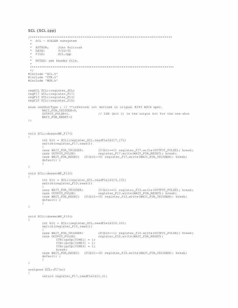
SCL (SCL.cpp)
/**************************************************************************** * SCL - SCALER subsystem * * AUTHOR: John Pultorak * DATE: 9/22/01 * FILE: SCL.cpp * * NOTES: see header file. * ***************************************************************************** */#include "SCL.h"#include "CTR.h"#include "MON.h"
regSCL SCL::register_SCL;regF17 SCL::register_F17;regF13 SCL::register_F13;regF10 SCL::register_F10;
enum oneShotType { // **inferred; not defined in orignal R393 AGC4 spec.WAIT_FOR_TRIGGER=0,OUTPUT_PULSE=1, // LSB (bit 1) is the output bit for the one-shotWAIT_FOR_RESET=2
};
void SCL::doexecWP_F17(){
int bit = SCL::register_SCL.readField(17,17);switch(register_F17.read()){case WAIT_FOR_TRIGGER: if(bit==1) register_F17.write(OUTPUT_PULSE); break;case OUTPUT_PULSE: register_F17.write(WAIT_FOR_RESET); break;case WAIT_FOR_RESET: if(bit==0) register_F17.write(WAIT_FOR_TRIGGER); break;default: ;}
}
void SCL::doexecWP_F13(){
int bit = SCL::register_SCL.readField(13,13);switch(register_F13.read()){case WAIT_FOR_TRIGGER: if(bit==1) register_F13.write(OUTPUT_PULSE); break;case OUTPUT_PULSE: register_F13.write(WAIT_FOR_RESET); break;case WAIT_FOR_RESET: if(bit==0) register_F13.write(WAIT_FOR_TRIGGER); break;default: ;}
}
void SCL::doexecWP_F10(){
int bit = SCL::register_SCL.readField(10,10);switch(register_F10.read()){case WAIT_FOR_TRIGGER: if(bit==1) register_F10.write(OUTPUT_PULSE); break;case OUTPUT_PULSE: register_F10.write(WAIT_FOR_RESET);
CTR::pcUp[TIME1] = 1;CTR::pcUp[TIME3] = 1;CTR::pcUp[TIME4] = 1;break;
case WAIT_FOR_RESET: if(bit==0) register_F10.write(WAIT_FOR_TRIGGER); break;default: ;}
}
unsigned SCL::F17x(){
return register_F17.readField(1,1);

}
unsigned SCL::F13x(){
return register_F13.readField(1,1);}
unsigned SCL::F10x(){
return register_F10.readField(1,1);}
void SCL::doexecWP_SCL(){
if(MON::SCL_ENAB) // if the scaler is enabled{
//write((read() + 1) % outmask());register_SCL.write((register_SCL.read() + 1));
}}
SEQ (SEQ.h)
/**************************************************************************** * SEQ - SEQUENCE GENERATOR subsystem * * AUTHOR: John Pultorak * DATE: 9/22/01 * FILE: SEQ.h * * VERSIONS: * * DESCRIPTION: * Sequence Generator for the Block 1 Apollo Guidance Computer prototype (AGC4). * * SOURCES: * Mostly based on information from "Logical Description for the Apollo * Guidance Computer (AGC4)", Albert Hopkins, Ramon Alonso, and Hugh * Blair-Smith, R-393, MIT Instrumentation Laboratory, 1963. * * NOTES: * ***************************************************************************** */#ifndef SEQ_H#define SEQ_H
#include "reg.h"
#define MAXPULSES 15#define MAX_IPULSES 5 // no more than 5 instruction-generated pulses active at any time
enum cpType { // **inferred; not defined in orignal R393 AGC4 spec.NO_PULSE=0,
// OUTPUTS FROM SUBSYSTEM ACI =1, // Carry inCLG =2, // Clear GCLCTR =3, // Clear loop counterCTR =4, // Loop counterGP =5, // Generate ParityKRPT =6, // Knock down Rupt priorityNISQ =7, // New instruction to the SQ registerRA =8, // Read ARB =9, // Read BRB14 =10, // Read bit 14RC =11, // Read CRG =12, // Read GRLP =13, // Read LPRP2 =14, // Read parity 2RQ =15, // Read QRRPA =16, // Read RUPT addressRSB =17, // Read sign bitRSCT =18, // Read selected counter addressRU =19, // Read sumRZ =20, // Read ZR1 =21, // Read 1R1C =22, // Read 1 complimentedR2 =23, // Read 2R22 =24, // Read 22R24 =25, // Read 24ST1 =26, // Stage 1ST2 =27, // Stage 2TMZ =28, // Test for minus zeroTOV =29, // Test for overflowTP =30, // Test parityTRSM =31, // Test for resumeTSGN =32, // Test signTSGN2 =33, // Test sign 2WA =34, // Write AWALP =35, // Write A and LPWB =36, // Write BWGx =37, // Write G (do not reset)

WLP =38, // Write LPWOVC =39, // Write overflow counterWOVI =40, // Write overflow RUPT inhibitWOVR =41, // Write overflowWP =42, // Write PWPx =43, // Write P (do not reset)WP2 =44, // Write P2WQ =45, // Write QWS =46, // Write SWX =47, // Write XWY =48, // Write YWYx =49, // Write Y (do not reset)WZ =50, // Write Z
// OUTPUTS FROM SUBSYSTEM A; USED AS INPUTS TO SUBSYSTEM B ONLY;// NOT USED OUTSIDE CPMRSC =51, // Read special and central (output to B only, not outside CPM)WSC =52, // Write special and central (output to B only, not outside CPM)WG =53, // Write G (output to B only, not outside CPM)
// OUTPUTS FROM SUBSYSTEM A; USED AS INPUTS TO SUBSYSTEM C ONLY;// NOT USED OUTSIDE CPMSDV1 =54, // Subsequence DV1 is currently activeSMP1 =55, // Subsequence MP1 is currently activeSRSM3 =56, // Subsequence RSM3 is currently active
// EXTERNAL OUTPUTS FROM SUBSYSTEM B//RA0 =57, // Read register at address 0 (A)RA1 =58, // Read register at address 1 (Q)RA2 =59, // Read register at address 2 (Z)RA3 =60, // Read register at address 3 (LP)RA4 =61, // Read register at address 4RA5 =62, // Read register at address 5RA6 =63, // Read register at address 6RA7 =64, // Read register at address 7RA10 =65, // Read register at address 10 (octal)RA11 =66, // Read register at address 11 (octal)RA12 =67, // Read register at address 12 (octal)RA13 =68, // Read register at address 13 (octal)RA14 =69, // Read register at address 14 (octal)RBK =70, // Read BNKWA0 =71, // Write register at address 0 (A)WA1 =72, // Write register at address 1 (Q)WA2 =73, // Write register at address 2 (Z)WA3 =74, // Write register at address 3 (LP)WA10 =75, // Write register at address 10 (octal)WA11 =76, // Write register at address 11 (octal)WA12 =77, // Write register at address 12 (octal)WA13 =78, // Write register at address 13 (octal)WA14 =79, // Write register at address 14 (octal)WBK =80, // Write BNKWGn =81, // Write G (normal gates)**W20 =82, // Write into CYRW21 =83, // Write into SRW22 =84, // Write into CYLW23 =85, // Write into SL
// THESE ARE THE LEFTOVERS -- THEY'RE PROBABLY USED IN SUBSYSTEM C//GENRST =86, // General Reset**CLINH =87, // Clear INHINT**CLINH1 =88, // Clear INHINT1**CLSTA =89, // Clear state counter A (STA)**CLSTB =90, // Clear state counter B (STB)**CLISQ =91, // Clear SNI**CLRP =92, // Clear RPCELL**INH =93, // Set INHINT**RPT =94, // Read RUPT opcode **SBWG =95, // Write G from memorySETSTB =96, // Set the ST1 bit of STBWE =97, // Write E-MEM from GWPCTR =98, // Write PCTR (latch priority counter sequence)**WSQ =99, // Write SQ

WSTB =100, // Write stage counter B (STB)**R2000 =101, // Read 2000 **
};
// INSTRUCTIONS
// Op Codes, as they appear in the SQ register.enum instruction {
// The code in the SQ register is the same as the op code for these// four instructions.TC =00, // 00 TC K Transfer Control 1 MCTCCS =01, // 01 CCS K Count, Compare, and Skip 2 MCTINDEX =02, // 02 INDEX K 2 MCTXCH =03, // 03 XCH K Exchange 2 MCT
// The SQ register code is the op code + 010 (octal). This happens because all// of these instructions have bit 15 set (the sign (SG) bit) while in memory. When the// instruction is copied from memory to the memory buffer register (G) to register// B, the SG bit moves from bit 15 to bit 16 and the sign is copied back into bit// 15 (US). Therefore, the CS op code (04) becomes (14), and so on.CS =014, // 04 CS K Clear and Subtract 2 MCTTS =015, // 05 TS K Transfer to Storage 2 MCTAD =016, // 06 AD K Add 2 or 3 MCTMASK =017, // 07 MASK K Bitwise AND 2 MCT
// These are extended instructions. They are accessed by executing an INDEX 5777// before each instruction. By convention, address 5777 contains 47777. The INDEX// instruction adds 47777 to the extended instruction to form the SQ op code. For// example, the INDEX adds 4 to the 4 op code for MP to produce the 11 (octal; the// addition generates an end-around-carry). SQ register code (the 7777 part is a // negative zero).MP =011, // 04 MP K Multiply 10 MCTDV =012, // 05 DV K Divide 18 MCTSU =013, // 06 SU K Subtract 4 or 5 MCT
};
enum subseq {TC0 =0,CCS0 =1,CCS1 =2,NDX0 =3,NDX1 =4,RSM3 =5,XCH0 =6,CS0 =7,TS0 =8,AD0 =9,MASK0 =10,MP0 =11,MP1 =12,MP3 =13,DV0 =14,DV1 =15,SU0 =16,RUPT1 =17,RUPT3 =18,STD2 =19,PINC0 =20,MINC0 =21,SHINC0 =22,NO_SEQ =23
};
enum scType { // identifies subsequence for a given instructionSUB0=0, // ST2=0, ST1=0SUB1=1, // ST2=0, ST1=1SUB2=2, // ST2=1, ST1=0SUB3=3 // ST2=1, ST1=1
};
enum brType {BR00 =0, // BR1=0, BR2=0BR01 =1, // BR1=0, BR2=1
BR10 =2, // BR1=1, BR2=0BR11 =3, // BR1=1, BR2=1NO_BR =4 // NO BRANCH
};
const int GOPROG =02000; // bottom address of fixed memory
class regSQ : public reg { public:
regSQ() : reg(4, "%02o") { }};
class regSTA : public reg { public:
regSTA() : reg(2, "%01o") { }};
class regSTB : public reg { public:
regSTB() : reg(2, "%01o") { }};
class regBR1 : public reg { public:
regBR1() : reg(1, "%01o") { }};
class regBR2 : public reg { public:
regBR2() : reg(1, "%01o") { }};
class regCTR : public reg { public:
regCTR() : reg(3, "%01o") { }};
class regSNI : public reg { public: regSNI() : reg(1, "%01o") { }};
class SEQ{public:
static void execWP_GENRST();static void execWP_WSQ(); static void execWP_NISQ();static void execWP_CLISQ();static void execWP_ST1();static void execWP_ST2();static void execWP_TRSM();static void execWP_CLSTA();static void execWP_WSTB();static void execWP_CLSTB();static void execWP_SETSTB();static void execWP_TSGN();static void execWP_TOV();static void execWP_TMZ();static void execWP_TSGN2();static void execWP_CTR();static void execWP_CLCTR();
static regSNI register_SNI; // select next intruction flagstatic cpType glbl_cp[MAXPULSES]; // current set of asserted control pulses
(MAXPULSES)
static char* cpTypeString[];
// Test the currently asserted control pulses; return true if the specified// control pulse is active.static bool isAsserted(cpType pulse);
// Return a string containing the names of all asserted control pulses.static char* getControlPulses();
static subseq glbl_subseq; // currently decoded instruction subsequence
static regSQ register_SQ; // instruction registerstatic regSTA register_STA; // stage counter Astatic regSTB register_STB; // stage counter Bstatic regBR1 register_BR1; // branch register1static regBR2 register_BR2; // branch register2static regCTR register_LOOPCTR; // loop counter
static char* instructionString[];};
#endif

SEQ (SEQ.cpp)
/**************************************************************************** * SEQ - SEQUENCE GENERATOR subsystem * * AUTHOR: John Pultorak * DATE: 9/22/01 * FILE: SEQ.cpp * * NOTES: see header file. * ***************************************************************************** */#include "SEQ.h"#include "ADR.h"#include "BUS.h"
regSNI SEQ::register_SNI; // select next intruction flagcpType SEQ::glbl_cp[]; // current set of asserted control pulses (MAXPULSES)
regSQ SEQ::register_SQ; // instruction registerregSTA SEQ::register_STA; // stage counter AregSTB SEQ::register_STB; // stage counter BregBR1 SEQ::register_BR1; // branch register1regBR2 SEQ::register_BR2; // branch register2regCTR SEQ::register_LOOPCTR; // loop countersubseq SEQ::glbl_subseq; // currently decoded instruction subsequence
char* SEQ::instructionString[] ={
"TC","CCS","INDEX","XCH","***","***","***","***","***","MP","DV","SU","CS","TS","AD","MASK"
};
char* SEQ::cpTypeString[] = {
"NO_PULSE",
// OUTPUTS FROM SUBSYSTEM A"CI", "CLG", "CLCTR", "CTR", "GP", "KRPT", "NISQ", "RA", "RB", "RB14", "RC", "RG", "RLP", "RP2", "RQ", "RRPA", "RSB", "RSCT", "RU", "RZ", "R1", "R1C", "R2", "R22", "R24", "ST1", "ST2", "TMZ", "TOV", "TP", "TRSM", "TSGN", "TSGN2", "WA", "WALP", "WB", "WGx", "WLP", "WOVC", "WOVI", "WOVR", "WP", "WPx", "WP2", "WQ", "WS", "WX", "WY", "WYx", "WZ",
// OUTPUTS FROM SUBSYSTEM A; USED AS INPUTS TO SUBSYSTEM B ONLY;// NOT USED OUTSIDE CPM//"RSC", "WSC", "WG",
// OUTPUTS FROM SUBSYSTEM A; USED AS INPUTS TO SUBSYSTEM C ONLY;// NOT USED OUTSIDE CPM//"SDV1", "SMP1", "SRSM3",
// EXTERNAL OUTPUTS FROM SUBSYSTEM B
//"RA0", "RA1", "RA2", "RA3", "RA4", "RA5", "RA6", "RA7", "RA10", "RA11", "RA12", "RA13", "RA14", "RBK", "WA0", "WA1", "WA2", "WA3", "WA10", "WA11", "WA12", "WA13", "WA14", "WBK", "WGn", "W20", "W21", "W22", "W23",
// THESE ARE THE LEFTOVERS -- THEY'RE PROBABLY USED IN SUBSYSTEM C//"GENRST", "CLINH", "CLINH1", "CLSTA", "CLSTB", "CLISQ", "CLRP", "INH", "RPT", "SBWG", "SETSTB", "WE", "WPCTR", "WSQ", "WSTB", "R2000"
};
void SEQ::execWP_GENRST(){
register_SQ.write(0);register_BR1.write(0);register_BR2.write(0);register_SNI.write(0);register_LOOPCTR.write(0);register_STA.write(0);register_STB.write(0);
}
void SEQ::execWP_WSQ(){
register_SQ.write(BUS::glbl_WRITE_BUS >> 12);}
void SEQ::execWP_NISQ(){
register_SNI.writeField(1,1,1); // change to write(1)??}
void SEQ::execWP_CLISQ(){
register_SNI.writeField(1,1,0); // change to write(0)??}
bool SEQ::isAsserted(cpType pulse){
for(unsigned i=0; i<MAXPULSES; i++)if(glbl_cp[i] == pulse) return true;
return false;}
char* SEQ::getControlPulses(){
static char buf[MAXPULSES*6];strcpy(buf,"");
for(unsigned i=0; i<MAXPULSES && glbl_cp[i] != NO_PULSE; i++){
strcat(buf, cpTypeString[glbl_cp[i]]);strcat(buf," ");
}//if(strcmp(buf,"") == 0) strcat(buf,"NONE");return buf;
}
void SEQ::execWP_ST1(){
register_STA.writeField(1,1,1);}

void SEQ::execWP_ST2(){
register_STA.writeField(2,2,1);}
void SEQ::execWP_TRSM(){
if(ADR::EQU_25()) register_STA.writeField(2,2,1);
}
void SEQ::execWP_CLSTA(){
register_STA.writeField(2,1,0);}
void SEQ::execWP_WSTB(){
register_STB.write(SEQ::register_STA.read()); }
void SEQ::execWP_CLSTB(){
register_STB.writeField(2,1,0);}
void SEQ::execWP_SETSTB(){
register_STB.writeField(2,1,1);}
void SEQ::execWP_TSGN(){
// Set Branch 1 FF// if sign bit is '1' (negative sign)
if(BUS::glbl_WRITE_BUS & 0100000) register_BR1.write(1);
else register_BR1.write(0);
}
void SEQ::execWP_TOV(){
// Set Branch 1 FF// if negative overflow (sign==1; overflow==0)
if((BUS::glbl_WRITE_BUS & 0140000) == 0100000) register_BR1.write(1);
else register_BR1.write(0);
// Set Branch 2 FF// if positive overflow (sign==0; oveflow==1)
if((BUS::glbl_WRITE_BUS & 0140000) == 0040000) register_BR2.write(1);
else register_BR2.write(0);
}
void SEQ::execWP_TSGN2(){
// Set Branch 2 FF// if sign bit is '1' (negative sign)

if(BUS::glbl_WRITE_BUS & 0100000) register_BR2.write(1);
else register_BR2.write(0);
}
void SEQ::execWP_TMZ(){
// Set Branch 2 FF// if minus zero
if(BUS::glbl_WRITE_BUS == 0177777) register_BR2.write(1);
else register_BR2.write(0);
}
void SEQ::execWP_CTR(){
register_LOOPCTR.write(register_LOOPCTR.read()+1);}
void SEQ::execWP_CLCTR(){
register_LOOPCTR.write(0);}

TPG (TPG.h)
/**************************************************************************** * TPG - TIME PULSE GENERATOR subsystem * * AUTHOR: John Pultorak * DATE: 9/22/01 * FILE: TPG.h * * VERSIONS: * * DESCRIPTION: * Time Pulse Generator and Start/Stop Logic for the Block 1 Apollo Guidance * Computer prototype (AGC4). * * SOURCES: * Mostly based on information from "Logical Description for the Apollo * Guidance Computer (AGC4)", Albert Hopkins, Ramon Alonso, and Hugh * Blair-Smith, R-393, MIT Instrumentation Laboratory, 1963. * * NOTES: * ***************************************************************************** */#ifndef TPG_H#define TPG_H
#include "reg.h"
// Start/Stop Logic and Time Pulse Generator Subsystem
enum tpType {STBY =0,PWRON =1,
TP1 =2, // TIME PULSE 1: start of memory cycle time (MCT)TP2 =3,TP3 =4,TP4 =5,TP5 =6,TP6 =7, // EMEM is available in G register by TP6TP7 =8, // FMEM is available in G register by TP7TP8 =9,TP9 =10,TP10 =11, // G register written to memory beginning at TP10TP11 =12, // TIME PULSE 11: end of memory cycle time (MCT)TP12 =13, // select new subsequence/select new instruction
SRLSE =14, // step switch releaseWAIT =15
};
class regSG : public reg { public: regSG() : reg(4, "%02o") { }
};
class TPG{public:
static void doexecWP_TPG();
static regSG register_SG;
static char* tpTypestring[];};
#endif

TPG (TPG.cpp)
/**************************************************************************** * TPG - TIME PULSE GENERATOR subsystem * * AUTHOR: John Pultorak * DATE: 9/22/01 * FILE: TPG.cpp * * NOTES: see header file. * ***************************************************************************** */#include "TPG.h"#include "MON.h"#include "SCL.h"#include "SEQ.h"#include "OUT.h"
char* TPG::tpTypestring[] = // must correspond to tpType enumerated type{
"STBY", "PWRON", "TP1", "TP2", "TP3", "TP4", "TP5", "TP6", "TP7", "TP8","TP9", "TP10", "TP11", "TP12", "SRLSE", "WAIT"
};
regSG TPG::register_SG; // static member
void TPG::doexecWP_TPG() {
unsigned mystate = register_SG.read();if(MON::PURST)
mystate = STBY;elseswitch(mystate){case STBY: if(!MON::PURST && ((!MON::FCLK) || SCL::F17x())) mystate = PWRON; break;case PWRON: if(((!MON::FCLK) || SCL::F13x())) mystate = TP1; break;
case TP1: mystate = TP2; break;case TP2: mystate = TP3; break;case TP3: mystate = TP4; break;case TP4: mystate = TP5; break;case TP5: mystate = TP6; break;case TP6: mystate = TP7; break;case TP7: mystate = TP8; break;case TP8: mystate = TP9; break;case TP9: mystate = TP10; break;case TP10: mystate = TP11; break;case TP11: mystate = TP12; break;case TP12:
if(SEQ::register_SNI.read() && OUT::register_OUT1.readField(8,8) && MON::SA)mystate = STBY;// the next transition to TP1 is incompletely decoded; it works because// the transition to STBY has already been tested.
else if((MON::RUN) || (!SEQ::register_SNI.read() && MON::INST))mystate = TP1;
elsemystate = SRLSE;
break;case SRLSE: if(!MON::STEP) mystate = WAIT; break;case WAIT:
if(MON::STEP || MON::RUN) mystate = TP1;
break;default: break;}register_SG.write(mystate);
}