
BL1B Electronic Structure and Correlation Effects in K0 ... · BL1B Electronic Structure and...
30
BL1B Electronic Structure and Correlation Effects in K 0.49 RhO 2 R. Okazaki 1 , Y. Nishina 1 , Y. Yasui 1 , S. Shibasaki 2 and I. Terasaki 1 1 Department of Physics, Nagoya University, Nagoya 464-8602, Japan 2 Department of Applied Physics, Waseda University, Tokyo 169-8555, Japan The layered cobalt oxide Na x CoO 2 is a fascinating material because of its highly unusual transport properties, i.e., a large Seebeck coefficient with low electrical resistivity [1], as well as a rich electronic phase diagram. With increasing Na content x, the system varies from a Pauli-paramagnetic metal to a Curie-Weiss metal through a charge-ordered insulator around x = 0.5. Furthermore, hydration induces a superconductivity near x = 0.3. To elucidate the origin of such intriguing phenomena in this material, the knowledge of the detailed electronic structure is crucially important. The optical conductivity spectra in Na x CoO 2 captured wide electronic structure [2,3], which can be assigned to the local density approximation (LDA) band structure. However, the LDA + Hubbard U calculations, which well explain the results of the angle-resolved photoemission spectroscopy studies on Na x CoO 2 , seriously worsen the consistency between the LDA and the optical conductivity spectra [4], puzzling a precise role of electron correlations for the electronic structure in this compound. Here we investigate an optical property of isostructural 4d-electron Rh oxide K 0.49 RhO 2 [5]. We used the beamline BL1B in UVSOR facility to measure the reflectivity spectra of K 0.49 RhO 2 single crystals in an energy region of 2 – 30 eV, which enables us to evaluate the optical conductivity through the Kramers-Kronig analysis. In Fig. 1 (a), we show the optical conductivity spectrum below 8 eV. The peak locations are well defined near 0.9, 3.1, and 5.5 eV as labeled by , , and , respectively. For comparison, we depict the room-temperature optical conductivity spectra of Na x CoO 2 in Fig. 1 (b), which were taken from previous reports [2,3]. In Na x CoO 2 , three conductivity peaks labeled by , , and are clearly recognized at 0.5, 1.6, and 3 eV, respectively. Within the LDA scheme, the peak corresponds to the transition between t 2g bands and the peak to t 2g -e g transition. The peak is responsible for the charge-transfer transition from occupied O 2p to unoccupied e g states, as schematically illustrated in Fig. 1 (c). The peak positions in K 0.49 RhO 2 are clearly shifted to higher energies relative to the spectra of Na x CoO 2 . It is also found that the peak widths are broader than those of Na x CoO 2 . These differences are naively captured by broader 4d orbitals in K 0.49 RhO 2 as schematically shown in Fig. 1(d). A large crystal-field splitting pushes the and peaks in Na x CoO 2 to higher energy and peaks in K 0.49 RhO 2 , respectively. The bandwidth of t 2g complex is expanded by broad orbitals of Rh 4d electrons, leading to a higher-energy shift of the peak as well. We also find that the effective mass of K 0.49 RhO 2 is nearly half that of Na x CoO 2 from a comparison of the spectrum weights. The electronic structure and correlation effects in K 0.49 RhO 2 are well described by the difference between Co 3d and Rh 4d orbitals. Fig. 1. Optical conductivity 1 ( ) of (a) K 0.49 RhO 2 and (b) Na x CoO 2 . The data for Na x CoO 2 was taken from previous reports [2,3]. The peak locations in K 0.49 RhO 2 (Na x CoO 2 ) spectra are labeled by ( ), ( ), and ( ), which correspond to the O 2p-e g , t 2g -e g , and t 2g -t 2g transitions, respectively, as illustrated in schematic energy diagrams (c,d). [1] I. Terasaki, Y. Sasago and K. Uchinokura, Phys. Rev. B 56 (1997) R12685. [2] N. L. Wang et al., Phys. Rev. Lett. 93 (2004) 237007. [3] J. Hwang, J. Yang, T. Timusk and F. C. Chou, Phys. Rev. B 72 (2005) 024549. [4] M. D. Johannes, I. I. Mazin and D. J. Singh, Phys. Rev. B 71 (2005) 205103. [5] R. Okazaki et al., Phys. Rev. B 84 (2011) 075110. 77
Transcript of BL1B Electronic Structure and Correlation Effects in K0 ... · BL1B Electronic Structure and...

BL1B
Electronic Structure and Correlation Effects in K0.49RhO2
R. Okazaki1, Y. Nishina1, Y. Yasui1, S. Shibasaki2 and I. Terasaki1 1Department of Physics, Nagoya University, Nagoya 464-8602, Japan
2Department of Applied Physics, Waseda University, Tokyo 169-8555, Japan
The layered cobalt oxide NaxCoO2 is a fascinating material because of its highly unusual transport properties, i.e., a large Seebeck coefficient with low electrical resistivity [1], as well as a rich electronic phase diagram. With increasing Na content x, the system varies from a Pauli-paramagnetic metal to a Curie-Weiss metal through a charge-ordered insulator around x = 0.5. Furthermore, hydration induces a superconductivity near x = 0.3.
To elucidate the origin of such intriguing phenomena in this material, the knowledge of the detailed electronic structure is crucially important. The optical conductivity spectra in NaxCoO2 captured wide electronic structure [2,3], which can be assigned to the local density approximation (LDA) band structure. However, the LDA + Hubbard U calculations, which well explain the results of the angle-resolved photoemission spectroscopy studies on NaxCoO2, seriously worsen the consistency between the LDA and the optical conductivity spectra [4], puzzling a precise role of electron correlations for the electronic structure in this compound. Here we investigate an optical property of isostructural 4d-electron Rh oxide K0.49RhO2 [5]. We used the beamline BL1B in UVSOR facility to measure the reflectivity spectra of K0.49RhO2 single crystals in an energy region of 2 – 30 eV, which enables us to evaluate the optical conductivity through the Kramers-Kronig analysis. In Fig. 1 (a), we show the optical conductivity spectrum below 8 eV. The peak locations are well defined near 0.9, 3.1, and 5.5 eV as labeled by , , and , respectively. For comparison, we depict the room-temperature optical conductivity spectra of NaxCoO2 in Fig. 1 (b), which were taken from previous reports [2,3]. In NaxCoO2, three conductivity peaks labeled by , , and are clearly recognized at 0.5, 1.6, and 3 eV, respectively. Within the LDA scheme, the peak corresponds to the transition between t2g bands and the peak to t2g-eg transition. The peak is responsible for the charge-transfer transition from occupied O 2p to unoccupied eg states, as schematically illustrated in Fig. 1 (c). The peak positions in K0.49RhO2 are clearly shifted to higher energies relative to the spectra of NaxCoO2. It is also found that the peak widths are broader than those of NaxCoO2. These differences are naively captured by broader 4d orbitals in K0.49RhO2 as schematically shown in Fig. 1(d). A large crystal-field splitting pushes the and peaks in NaxCoO2 to higher energy and peaks in K0.49RhO2, respectively. The bandwidth of t2g complex is expanded by broad orbitals of Rh 4d electrons, leading to a higher-energy shift of the
peak as well. We also find that the effective mass of K0.49RhO2 is nearly half that of NaxCoO2 from a comparison of the spectrum weights. The electronic structure and correlation effects in K0.49RhO2 are well described by the difference between Co 3d and Rh 4d orbitals.
Fig. 1. Optical conductivity 1( ) of (a) K0.49RhO2 and (b) NaxCoO2. The data for NaxCoO2 was taken from previous reports [2,3]. The peak locations in K0.49RhO2 (NaxCoO2) spectra are labeled by ( ), ( ), and ( ), which correspond to the O 2p-eg, t2g-eg, and t2g-t2g transitions, respectively, as illustrated in schematic energy diagrams (c,d). [1] I. Terasaki, Y. Sasago and K. Uchinokura, Phys. Rev. B 56 (1997) R12685. [2] N. L. Wang et al., Phys. Rev. Lett. 93 (2004) 237007. [3] J. Hwang, J. Yang, T. Timusk and F. C. Chou, Phys. Rev. B 72 (2005) 024549. [4] M. D. Johannes, I. I. Mazin and D. J. Singh, Phys. Rev. B 71 (2005) 205103. [5] R. Okazaki et al., Phys. Rev. B 84 (2011) 075110.
77

BL2A
Characterization of Phosphorus Doped Titanium Oxide T. Kurisaki, M. Iwase, Y. Nagino, S. Yokoyama and H. Wakita
Department of Chemistry, Faculty of Science, Fukuoka University, Nanakuma, Jonan-ku, Fukuoka 814-0180, Japan
Doping TiO2 with nonmetal such as nitrogen [1], carbon [2] and sulfur has received a lot of attention in recent years since it can extend the photoresponse of TiO2 from ultra violet to the visible region, which is advantageous for using the sunlight as the energy source. As for Phosphorus-doped TiO2 with visible-light photocatalytic activity, two kinds of P-TiO2 [3,4] prepared using phosphate as precursor of P has been reported. However, some reports showed that P-TiO2 prepared using phosphate cannot absorb visible-light. Thus, we attempted to prepare P-TiO2 using phosphide as a new method. P-TiO2 was synthesized through the hydrolysis of titanium tetraisopropoxide in suspension containing TiP compound [5], which was prepared by the treatment of titanium tetrachloride with cyclohexylphosphine. The synthesized P-TiO2 nanoparticles exhibit a visible-light photocatalytic activity. However, the electronic structure of phosphorus in the P-TiO2 nanoparticles is not well known.
For various light element compounds, we have studied the electronic structure by X-ray absorption spectroscopy [6]. These results suggested that there is a correlation between XANES spectra and the local structures.
In this work, we performed the XANES spectra measurement about various phosphorus doped titanium oxides and reference samples such as titanium phosphide (TiP). The obtained experimental XANES spectra are analyzed using the calculated theoretical spectra from DV-X calculations. The XANES spectra were measured at BL2A of the UVSOR in the Institute of Molecular Science, Okazaki [7]. The ring energy of the UVSOR storage ring was 750MeV and the stored current was 300 mA. P K-edge XANES spectra were recorded in the regions of 2125-2270eV by use of two InSb crystals. The absorption was monitored by the total electron yield using a photomultiplier. The samples were spread into the carbon tape on the first photodynode made of CuBe of the photomultiplier.
Figure 1 shows the observed P K-edge XANES spectra for the TiP and the phosphorus doped titanium oxide. The P K-edge XANES spectra of TiP and P-TiO2 show different peak profiles at second peaks. The peaks that appear at approximately 2176 and 2185 eV on observed XANES spectrum of TiP are labeled A and B. The peak positions of A and B are estimated to the P-3 and P5+. On the other hand, the observed XANES spectrum of P-TiO2 showed only one peak at 2186 eV. The result suggests that phosphorus in the synthesized P-TiO2 nanoparticle surface exists as phosphoric acid. We are going to try
to analyze this change from comparison of P K-edge XANES and calculated spectra by DV-X molecular orbital calculations. Fig. 1. Observed P K-edge XANES spectra of TiP and P-TiO2. [1] R. Asahi et al., Science 293 (2001) 269. [2] Y. Nosaka et al., Sci. Tech. Adv. Mater. 6 (2005) 143. [3] L. Lin and W. Lin, Chem. Lett. 34 (2005) 284. [4] Q. Shi et al., J. Mol. B: Enzym. 43 (2006) 44. [5] T. S. Lewkebandara et al., Chem. Mater. 7 (1995) 1053. [6] T. Kurisaki et al., Anal. Sci. 24 (2008) 1385. [7] S. Murata et al., Rev. Sci. Instrum. 63 (1992) 1309.
2160 2170 2180 2190 2200 2210 2220
TiP P-TiO2
Nor
mal
ized
Inte
nsity
/ a.u
.
Energy / eV
A B
78
BL2A
Mg-K Edge XAFS Measurement of Mg Doped Hydroxyapatite by Fluorescence Mode
M. Sato1, Y. Nishio2, T. Nagayasu2 and A. Nakahira1, 21Kansai Center for Industrial Materials Research, Tohoku University, Osaka 599-8531, Japan
2Department of Material Science and Engineering, Osaka Prefecture University, Osaka 599-8531, Japan
Hydroxyapatite (Ca10(PO4)6(OH)2, HAp) has been well understood as an alternate materials of our hard tissue because of their excellent osteoconductivity and biocompatibility. Furthermore, because HAp also has good protein adsorption ability and ion exchange ability, many studies for bioactivity and dissolution behavior of Mg, Mn, Fe, Si, Zn doped HAp have been performed. Since we could not obtain effective data of Mg doped HAp by total electron yield mode so far, we tried fluorescence mode and investigated a local structure of around Mg atom of Mg doped HAp. In this study, Mg doped HAp were prepared by microwave assisted hydrothermal process, respectively, and local structure of around P atom was investigated by XAFS measurement.
0.1 mol/l Ca(NO3)2, (NH4)2HPO4 and Mg(NO3)solutions were used as starting materials. These solutions were mixed up each other becoming the ratio of Ca to P of 1.67 and the ratio of Mg from 1 to 15 mol% for Ca solution, respectively. Mixed solutions were set into autoclave and hydrothermally treated at 423 K for 60 min. with irradiation of microwave (2.45 GHz). After that, they were filtered and dried at 323 K for overnight. Mg-K edge XANES spectra of Mg doped HAp powders were measured by fluorescence method at room temperature using beryl double-crystal monochrometer at BL2A station of UVSOR and obtained spectra were compared to that obtained by a total electron yield mode.
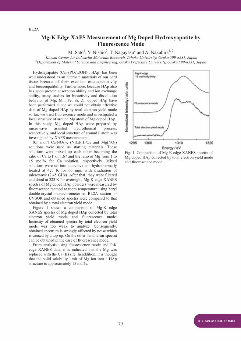
Figure 1 shows a comparison of Mg-K edge XANES spectra of Mg doped HAp collected by total electron yield mode and fluorescence mode.Intensity of obtained spectra by total electron yield mode was too weak to analyze. Consequently, obtained spectrum is strongly affected by noise which is caused by a top-up. On the other hand, clear spectra can be obtained in the case of fluorescence mode.
From analysis using fluorescence mode and P-K edge XANES data, it is indicated that the Mg was replaced with the Ca (II) site. In addition, it is thought that the solid solubility limit of Mg ion into a HAp structure is approximately 15 mol%.
Fig. 1. Comparison of Mg-K edge XANES spectra of Mg doped HAp collected by total electron yield mode and fluorescence mode.
79

BL2A
Investigation of Local Structure of Si-K and Al-K Edge in Zeolites Prepared from Waste Materials
M. Sato1, Y. Takamatsu2, K. Kumadani2 and A. Nakahira1, 21Kansai Center for Industrial Materials Research, Tohoku University, Osaka 599-8531, Japan
2Department of Material Science and Engineering, Osaka Prefecture University, Osaka 599-8531, Japan
The depletion of natural resources is one of the our serious problems. Therefore, the development of the novel recycling technology has been performed energetically. Blast furnace slag (BF slag) is one of the waste materials that the development of the effective recycling technology and establishment of recycle system become the urgent assignment. The BF slag has been produced approximately 25 million tons per year and recycled as Portland cement, base coarse materials, fine aggregate for concrete and ground improvement materials, etc. However, recycling rate of BF slag is insufficient by comparing to the amount of generation. In this study, A, P and Y type zeolite were prepared using BF slag as a starting material to reduce an emission of waste materials, and local structure of BF slag and its products were investigated.
Water cooled BF slag was ground to become their particle size less than 70 m. Ground slag powder was undergone an acid treatment to remove a Ca component. And then, Ca removed slag powder was hydrothermally treated in 0.23 mol/l NaOH solution at 368 K for 48 h. In this study, the ratio of Si to Al was changed in the range from 0.5 to 2.4. Si-K and Al-K edge XANES spectra of samples were measured by a total electron yield mode at room temperature using KTP double-crystal monochromator at BL2A station of UVSOR.
Figure 1 shows Si-K edge XANES spectra of water cooled BF slag, acid treated BF slag and A type zeolite prepared using acid treated BF slag. The local structure around Si atom of BF slag is relatively amorphous and changed by acid treatment. Furthermore, the local structure of A type zeolite prepared using slag as a starting material differed from commercial A type zeolite and that synthesized using reagents.
Figure 2 shows Al-K edge XANES spectra of A and P type zeolites prepared using acid treated BF slag. Obtained spectra of A type zeolite prepared using BF slag was different from the result of Si-K edge spectra, and similar spectra to that of commercial A type zeolite was obtained. This result indicates that the local structure of around Al atom of sample is almost same.
Fig. 1. Si-K edge XANES spectra of water cooled BF-slag and its products.
Fig. 2. Al-K edge XANES spectra of water cooled BF-slag and its products.
80
BL2A
Investigation of Local Structure of P-K Edge in Fe, Mg and Mn Doped Hydroxyapatite
M. Sato1, Y. Kawabe2, S. Misu2, S. Hayashi2 and A. Nakahira1, 21Kansai Center for Industrial Materials Research, Tohoku University, Osaka 599-8531, Japan
2Department of Material Science and Engineering, Osaka Prefecture University, Osaka 599-8531, Japan
Hydroxyapatite (Ca10(PO4)6(OH)2, HAp) has been well understood as a alternate materials of our hard tissue because of their excellent osteoconductivity and biocompatibility. Furthermore, because HAp also has good protein adsorption ability and ion exchange ability, many studies for bioactivity and dissolution behavior of Mg, Mn, Fe, Si, Zn doped HAp have been performed.
In this study, Fe, Mg and Mn doped HAp were prepared by conventional wet process, hydrothermal process and microwave assisted hydrothermal process, respectively, and local structure around P atom was investigated by XAFS measurement.
0.1 mol/l Ca(NO3)2, (NH4)2HPO4 and FeCl3,Mg(NO3) and MnCl2 solutions were used as starting materials. These solutions were mixed up each other becoming the ratio of Ca to P of 1.67 and the ratio of Fe from 0.1 to 1 mol%, Mg from 1 to 15 mol% and Mn from 1 to 5 mol% for Ca solution, respectively. In the case of wet process, mixed solution was aged for 1 h at room temperature. For the hydrothermal and microwave assisted hydrothermal process, mixed solutions were set into autoclave and samples were prepared at 423 K for each preparation time. After that, they were filtered and dried at 323 K for overnight. P-K edge XANES spectra of obtained HAp powders were measured in a total electron yield mode at room temperature using InSb double-crystal monochrometer at BL2A station of UVSOR.
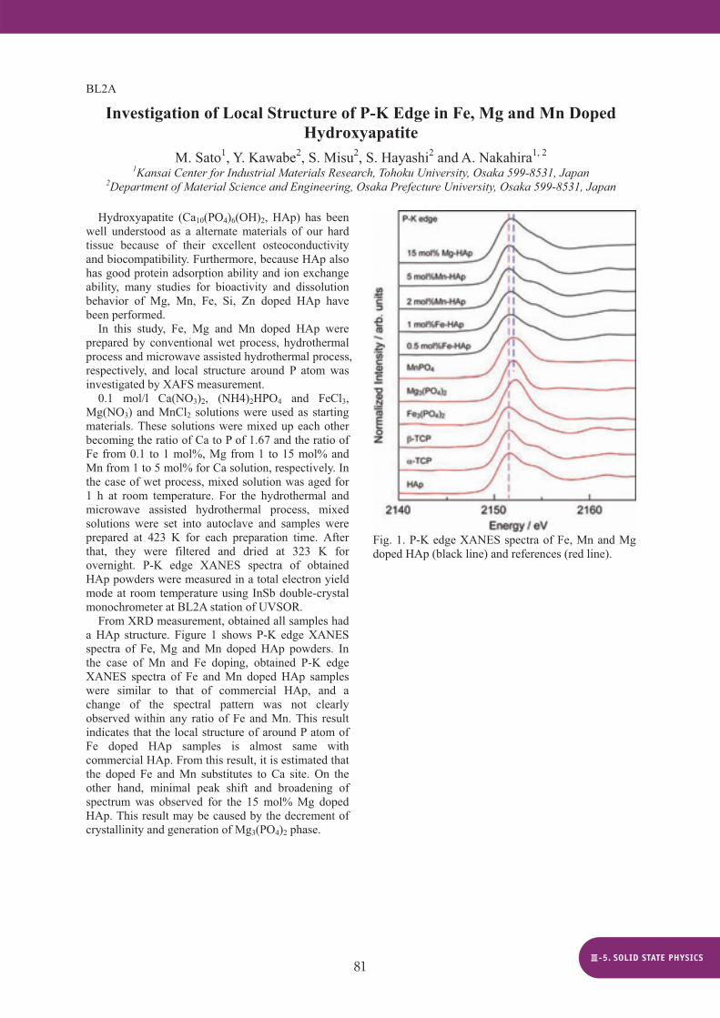
From XRD measurement, obtained all samples had a HAp structure. Figure 1 shows P-K edge XANES spectra of Fe, Mg and Mn doped HAp powders. In the case of Mn and Fe doping, obtained P-K edge XANES spectra of Fe and Mn doped HAp samples were similar to that of commercial HAp, and a change of the spectral pattern was not clearly observed within any ratio of Fe and Mn. This result indicates that the local structure of around P atom of Fe doped HAp samples is almost same with commercial HAp. From this result, it is estimated that the doped Fe and Mn substitutes to Ca site. On the other hand, minimal peak shift and broadening of spectrum was observed for the 15 mol% Mg doped HAp. This result may be caused by the decrement of crystallinity and generation of Mg3(PO4)2 phase.
Fig. 1. P-K edge XANES spectra of Fe, Mn and Mg doped HAp (black line) and references (red line).
81
BL3B
Energy Transfer Caused by Emission Reabsorption in CsI:Ag Crystals T. Kawai1, S. Nagata1 and T. Hirai2
1Graduate School of Science, Osaka Prefecture University, Sakai 599-8531, Japan 2Faculty of Science and Engineering, Ritsumeikan University, Kusatsu 525-8577, Japan
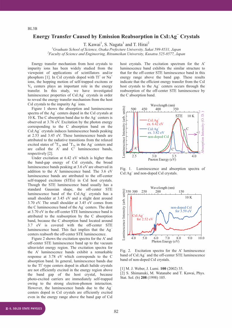
Energy transfer mechanism from host crystals to impurity ions has been widely studied from the viewpoint of applications of scintillators and/or phosphors [1]. In CsI crystals doped with Tl+ or Na+ ions, the hopping motion of self-trapped excitons or Vk centers plays an important role in the energy transfer. In this study, we have investigated luminescence properties of CsI:Ag crystals in order to reveal the energy transfer mechanism from the host CsI crystals to the impurity Ag ions. Figure 1 shows the absorption and luminescence spectra of the Ag centers doped in the CsI crystals at 10 K. The C absorption band due to the Ag centers is observed at 3.76 eV. Excitation by the photon energy corresponding to the C absorption band on the CsI:Ag crystals induces luminescence bands peaking at 2.53 and 3.45 eV. These luminescence bands are attributed to the radiative transitions from the relaxed excited states of 3T1u and 1T1u in the Ag centers and are called the A’ and C’ luminescence bands, respectively [2].
Under excitation at 6.42 eV which is higher than the band-gap energy of CsI crystals, the broad luminescence bands peaking at 3.6 eV are observed in addition to the A’ luminescence band. The 3.6 eV luminescence bands are attributed to the off-center self-trapped excitons (STEs) in CsI host crystals. Though the STE luminescence band usually has a standard Gaussian shape, the off-center STE luminescence band of the CsI:Ag crystals has a small shoulder at 3.45 eV and a slight dent around 3.70 eV. The small shoulder at 3.45 eV comes from the C luminescence band of the Ag centers. The dent at 3.70 eV in the off-center STE luminescence band is attributed to the reabsorption by the C absorption band, because the C absorption band located around 3.7 eV is covered with the off-center STE luminescence band. This fact implies that the Ag centers reabsorb the off-center STE luminescence.
Figure 2 shows the excitation spectra for the A’ and off-center STE luminescence band up to the vacuum ultraviolet energy region. The excitation spectra for the A’ luminescence bands exhibit a remarkable response at 3.78 eV which corresponds to the C absorption band. In general, luminescence bands due to the Tl+-type centers doped in alkali halide crystals are not efficiently excited in the energy region above the band gap of the host crystal, because photo-excited carriers are immediately self-trapped owing to the strong electron-phonon interaction. However, the luminescence bands due to the Ag centers doped in CsI crystals are efficiently excited even in the energy range above the band gap of CsI
host crystals. The excitation spectrum for the A’ luminescence band exhibits the similar structure to that for the off-center STE luminescence band in this energy range above the band gap. These results indicate that the efficient energy transfer from the CsI host crystals to the Ag centers occurs through the reabsorption of the off-center STE luminescence by the C absorption band.
2.5 3.0 3.5 4.0
350400450500
0
1
2
Pnoton Energy (eV)
Lum
ines
cenc
e In
tens
ity (a
rb. u
nits
)
Abs
orpt
ion
Inte
nsity
(O. D
. )
10 K
A' C'
CsI:Ag-
ex. 6.42 eV
non-doped CsI
CsI:Ag-
ex. 3.82 eV C
Wavelength (nm)
STE
Fig. 1. Luminescence and absorption spectra of CsI:Ag and non-doped CsI crystals.
4.0 5.0 6.0 7.0 8.0 9.0 10.0
150200250300350
Photon Energy (eV)Lum
ines
cenc
e In
tens
ity (a
rb. u
nits
) Wavelength (nm)
CsI:Ag-
for 2.52 eV
10 K
non-doped CsI for 3.59 eV
Fig. 2. Excitation spectra for the A’ luminescence band of CsI:Ag and the off-center STE luminescence band of non-doped CsI crystals. [1] M. J. Weber, J. Lumi. 100 (2002) 35. [2] S. Shimanuki, M. Watanabe and T. Kawai, Phys. Stat. Sol. (b) 208 (1998) 105.
82

BL3B
Relaxed Exciton Luminescence of CsCl Heavily Doped with CsI N. Ohno and A. Ohno
Graduate School of Engineering, Osaka Electro-Communication University, Neyagawa, Osaka 572-8530, Japan
Extensive studies have been made on luminescence arising from localized relaxed excitons in alkali chlorides containing iodine impurities. Stimulation in iodine absorption bands of dilute I–-doped alkali chlorides produces characteristic luminescence bands under excitation with UV light or with X-rays at low temperatures. These luminescence bands have been well explained in terms of localized relaxed excitons at ICl– molecule (I– monomer) and a complex of two iodine ions (I– dimer) [1,2]. However, optical and luminescence properties of heavily iodine-doped alkali chloride crystals have not been examined sufficiently for applying to high efficient scintillation materials. The authors have reported luminescence properties of KCl heavily doped with KI so far [3]. The present report describes the results of CsCl heavily doped with CsI. The crystals of CsCl:I were grown by the Bridgeman method from reagent grade CsCl added with an appropriate amount of CsI (up to 5 mol %).The optical measurements were made at 6 K.
The luminescence spectra excited with photons near the exciton absorption region of CsCl were almost the same as those of the previous studies [3]: two luminescence bands peaking at 3.95 eV (mono- mer emission) and 5.12 eV (dimer emission) are found at 6 K. Photoexcitation spectra detected at 5.11 eV for various CsI mol % of CsCl:I crystals are shown in Fig. 1. The each spectrum has been normalized at unity at the maximum. The excitation peaks at 6.50 and 6.65 eV of 0.01 mol % crystal move toward the lower energy side with increasing CsI concentration. The low energy shift of the excitation bands suggests that there coexist dimers, trimers and lager sizes of I – ions (CsI cluster) in heavily-doped CsCl:I crystal as can been seen in the case of heavily-doped KCl:I [4].
The luminescence energies of the trimers and clusters of I – ions in heavily doped CsCl:I crystals are expected to be different from that of I– dimers. We have examined the photoluminescence spectra excited at various photon energies. The results for 1 mol %crystal are shown in Fig. 2. It is clearly confirmed that the peak energy of the luminescence band moves towards the low energy side when excited with lower photon energy. These luminescence bands are supposed to be the composite bands due to radiative annihilation of the relaxed exciton at dimers, trimers and clusters of I – ions [4].
In CsCl crystals containing CsI above 1 mol %,there exists a small amount of dimer centers as compared with monomers, and moreover the amount of trimers and clusters of CsI is extremely smaller than those of monomers and dimers. However, the luminescence intensities of such large-sized centers
are found to be comparable with that of the dimer emission. This fact suggests that the excitons trapped in CsI clusters in heavily doped CsCl:I crystals would give the high luminescence efficiency. The similar mechanism has been reported in and heavily-doped KCl:I [4] and CsI:Na systems [5], where the observed luminescence enhancement originates from excitons in small-sized KI or NaI particles in host crystals.
Fig. 1. Photoexcitation spectra of CsCl:I crystals detected at 5.11 eV for various CsI mol % at 6 K.
Fig. 2. Photoluminescence spectra of CsCl:I (1 mol %)excited at various photon energies at 6 K.
[1] N. Nagasawa, J. Phys. Soc. Jpn. 27 (1969) 1535. [2] K. Kan’no, K. Tanaka and T. Hayashi, Rev. Solid State Sciences 4 (1990) 383, and references therein. [3] M. Yoshida and N. Ohno, Proc. Int. Conf. on Excitonic Processes in Condensed Matter (1996) 231. [4] A. Ohno and N. Ohno, Phys. Status Solidi C 8(2011) 112. [5] M. Nakayama, N. Ando, T. Miyoshi, J. Hiraiand H. Nishimura, Jpn. J. Appl. Phys. 41 (2002) L263.
4.5 5.0 5.50
3
6
Photon Energy [eV]
Inte
nsity
[a. u
.]
6.44 eV6.28 eV6.20 eV6.12 eV6.05 eV
CsCl:I 6K1mol%
6 7 80
0.5
1 CsCl:I 6K
0.01mol%1mol%3mol%
Nor
mal
ized
Inte
nsity
Photon Energy [eV]
5.11 eV
83

BL3B
Origin of Luminescence Bands in NaBi(WO4)2 Crystals M. Kitaura1, M. Fujita2, A. Ohnishi1, M. Sasaki1 and Sangeeta3
1Department of Physics, Facility of Science, Yamagata University, Yamagata 990-8560, Japan 2Japan Coast Guard Academy, Kure 737-8512, Japan
3Bhabha Atomic Research Center, Munbai 400 085, India
NaBi(WO4)2 belongs to the family of double tungstates expressed by the chemical formula NaT(WO4)2, in which T is occupied by trivalent cations. This material attracts interest for practical use as Cerenkov radiator to detect ultra high-energy radiation and charged particles. Despite of such an important material in high-energy physics experiment, optical properties of NaBi(WO4)2 have not been much investigated, as compared to other metal tungstates. In the present study, reflectivity and photoluminescence spectra of NaBi(WO4)2 have been measured using synchrotron radiation.
The crystals of NaBi(WO4)2 were provided from Bhabha Atomic Research Centre, Mumbai, India. They were grown from melt by the Czochralski method. The samples used in our experiment were attached at the cold finger of a LHe flow-type cryostate, and cooled down at 10 K. The reflectivity spectra were measured using a calibrated silicon diode in the measurement chamber. The photo- luminescence spectra were measured for variousexcitation wavelength by the combination of a grating monochromator and a CCD detector.
Figure 1 shows the contour plot of excitation- emission spectra of NaBi(WO4)2 (lower part), together with reflectivity spectrum (upper part). These data were measured at 10 K. A prominent peak is observed at 312 nm in the reflectivity spectrum. An emission band appears at 538 nm under excitation with photons around 340 nm. As the excitation wavelength is decreased from 340 nm to 320 nm, the 538 nm band is weakened, and another band appears at 484 nm. This band is predominantly observed under excitation in shorter excitation wavelength. These results are almost agreement with the results by Tyagi et al. [1].
Two emission bands are observed at 484 and 538 nm in NaBi(WO4)2 excited by photons in the fundamental absorption region. The 484 and 538 nm bands are similar to the blue (443 nm) and green (551 nm) bands in PbWO4, respectively. Itoh et al. [2] have explained the origin of these bands as follows: The blue band is ascribed to radiative decay of excitons self-trapped on regular WO4 tetrahedra, while the green band is likely assigned to excitons localized on WO6 octahedra of inclusions. NaBi(WO4)2crystallizes in the scheelite structure in which W ions locate inside tetrahedrons of four O ions. It is thus more likely that the 2.65 eV band is linked to regular WO4 tetrahedra. The 2.34 eV band may be due to WO6 octahedra, because there is the possibility that sodium tungstates composed of WO6 octahedra, e.g.,
NaWO3 and Na2W2O7, are included as low temperature phases. Decay kinetics of the 2.65 and 2.34 eV bands is now in investigation with Nd3+:YAG laser system, in order to clarify excited state dynamics of the self-trapped excitons of complex molecular ion type.
Fig. 1. Reflectivity spectra (upper part) and contour plot of excitation-emission spectra (lower part) of NaBi(WO4)2 measured at 10K.
[1] M. Tyagi et al., J. Lumi. 132 (2012) 41. [2] M. Itoh et al., Phys. Rev. B 62 (2000) 12825.
84

BL4B
Valence State Analysis of Co Ions in Pr1-xCaxCoO3-
T. Yoshioka1 and T. Yamamoto1, 2 1Faculty of Science and Engineering, Waseda University, Tokyo169-8555, Japan
2Institute of Condensed-Matter Science, Waseda University, Tokyo 169-8555, Japan
Rare-earth cobaltates, R1-xAxCoO3- (R = rare-earth, A = alkaline-earth), have been extensively studied for last fifty years because of their characteristic thermal, electrical, and magnetic properties [1-3]. For a thorough understanding of such properties, it is necessary to investigate the charge compensation mechanism due to the doping of the alkaline-earth ions in RCoO3. However, the mechanisms of charge compensation have not yet been thoroughly understood for these rare-earth cobaltates with alkaline-earth ions. In this study, the valence state analysis of Co ions in Pr1-xCaxCoO3- (x=0, 0.5 are carried out by the Co-L3 X-ray absorption near-edge structure (XANES) measurements at different temperature.
All Pr1-xCaxCoO3- samples were synthesized by the conventional solid-state reaction method. Co-L3 XANES spectra were recorded at BL4B in UVSOR using the total-electron-yield (TEY) method. All the sample powders were mounted on carbon adhesive tape. Synchrotron radiation from the storage ring was monochromatized by a varied-line-spacing plane grating (800 lines/mm). The energy resolution of the incident beams (E/ E) was set to 3000 by tuning the slit width at the upper and lower reaches of the grating. To see a temperature dependence of the Co-L3 XANES spectra, all the spectra were collected at room temperature and 105 K.
Prior to the XANES analysis, all the samples were characterized by the X-ray diffraction (XRD). No extra peaks were found in the observed XRD patterns except for those of the perovskite structured Pr1-xCaxCoO3- . Then the samples were determined to be crystallized in a single-phased orthorhombic perovskite structure (Pbnm).
Observed Co-L3 XANES spectra of PrCoO3 and Pr0.5Ca0.5CoO3- are compared in Fig. 1. In order to investigate the difference in the spectral profiles among these two, the observed spectra were deconvoluted into three components by using Gaussian functions (dashed lines in Fig. 1). It is found that relative intensity of peak A to B increases and peak C to B decrease with doping Ca2+ ions both at room temperature and 105K. In order to see the change in spectral profiles of Co-L3 XANES quantitatively, the relative intensities of peaks A and C to B, i.e., IA/IB and IC/IB, respectively, are plotted in Figs. 2(a) and (b), respectively.
As shown in Fig. 2, the relative intensities of peak A and C to B increase and decrease, respectively, with increasing of doped Ca2+ ions both at room temperature and 105K. Furthermore, if we compare
the spectra at 105K to the spectra of room temperature, the relative intensity IA/IB and IC/IB is smaller and larger, respectively. These experimental results suggest that the distributions of Co 3d band of Pr1-xCaxCoO3- are different between at room temperature and 105K.
0
50
100PrCoO3
RT
Nor
mal
ized
Inte
nsity
(a)
A
B
C
772 776 7800
50
100Pr0.5Ca0.5CoO3-
RT
Energy (eV)
A
B
C
0
50
100PrCoO3
105K
Nor
mal
ized
Inte
nsity
(b)
A
B
C
772 776 7800
50
100Pr0.5Ca0.5CoO3-
105K
Energy (eV)
A
B
C
Fig. 1. Observed Co-L3 XANES spectra of PrCoO3 and Pr0.5Ca0.5CoO3- (a) at room temperature and (b) at 105K. Dashed lines denote spectra deconvoluted into three components of the Gaussian function.
0 0.25 0.50
0.1
0.2
0.3
Ca concentration, x
Rela
tive
inte
nsity
, IA
/I B
(a)
0 0.25 0.5
0.4
0.5
Ca concentration, x
Rela
tive
inte
nsity
, IC/I B
(b)
RT
105K
Fig. 2. Relative intensities of (a) Peak A to B, IA/IB, and (b) Peak C to B, IC/IB in Co-L3 XANES spectra of Pr1-xCaxCoO3- (x=0, 0.5 as a function of the concentration of Ca2+ ions.
[1] G. Ch. Kostogloudis et al., Solid State Ionics 106 (1998) 207. [2] H. Masuda et al., J. Phys. Soc. Jpn. 72 (2003) 873. [3] S. Tsubouchi et al., Phys. Rev. B 69 (2004) 144406. [4] J. Zhou et al., J. Phys.: Condens. Matter 20 (2008) 055222.
85
BL5U
Angle-Resolved Photoemission Spectroscopy of a Mixed Valence System Sm1-xYxS
K. Imura1, T. Hajiri1, 2, M. Kaneko2, Y. Nishi3, H. S. Suzuki4, N. K. Sato3, T. Ito2,M. Matsunami1, 5 and S. Kimura1, 5
1UVSOR Facility, Institute for Molecular Science, Okazaki 444-8585, Japan 2Graduate School of Engineering, Nagoya University, Nagoya 464-8603, Japan
3Graduate School of Science, Nagoya University, Nagoya 464-8602, Japan 4Nuclear Scattering Group, National Institute for Materials Science, Tsukuba 305-0047, Japan
5School of Physical Sciences, The Graduate University for Advanced Studies, Okazaki 444-8585, Japan
Samarium monosulfide (SmS) is a prototypical compound that exhibits an insulator-to-metal transition by applying external pressure. This phase transition is accompanied by a color change from black to golden-yellow, namely B-G transition. The energy gap of about Eg ~ 0.1 eV evaluated by an electrical resistivity measurement at ambient pressure decreases forward a critical pressure of the B-G transition. Although angle resolved photoemission spectroscopy (ARPES) is one of powerful techniques to study electronic structure as well as a mechanism of this transition, unfortunately, pressure study is impossible.
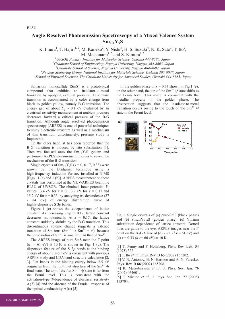
On the other hand, it has been reported that the B-G transition is induced by site substitution [1]. Then we focused onto the Sm1-xYxS system and performed ARPES measurement in order to reveal the mechanism of the B-G transition. Single crystals of Sm1-xYxS (x = 0, 0.17, 0.33) were grown by the Bridgman technique using a high-frequency induction furnace installed at NIMS [Figs. 1 (a) and 1 (b)]. ARPES measurement on these crystals was performed at the VUV-ARPES beamline BL5U of UVSOR. The obtained inner potential V0values 13.4 eV for x = 0, 13.7 eV for x = 0.17 and 15.2 eV for x = 0.33, by analyzing h -dependence (27 - 84 eV) of energy distribution curve of highly-dispersive S 3p bands. Figure 1 (c) shows the x-dependence of lattice constant. As increasing x up to 0.17, lattice constant decreases monotonically. At x = 0.17, the lattice constant suddenly shrinks by the B-G transition. This discontinuous volume change suggests a valence transition of Sm ions (Sm2+ Sm3+ + e-), because the ionic radius of Sm3+ is smaller than that of Sm2+.
The ARPES image of pure-SmS near the point (h = 61 eV) at 10 K is shown in Fig. 1 (d). The dispersive feature of the S 3p bands at the binding energy of about 3.2-6.5 eV is consistent with previous ARPES study and LDA band structure calculation [2, 3]. Flat bands in the binding energy below 2.5 eV originates from the multiplet structure of the Sm2+ 4ffinal state. The top of the flat Sm2+ 4f state is far from the Fermi level. This is consistent with the activation-type T-dependence of electrical resistivity
(T) [4] and the absence of the Drude response of the optical conductivity ( ) [5].
In the golden phase of x = 0.33 shown in Fig.1 (e), on the other hand, the top of the Sm2+ 4f state shifts to the Fermi level. This result is consistent with the metallic property in the golden phase. The observation suggests that the insulator-to-metal transition occurs owing to the touch of the Sm2+ 4fstate to the Fermi level.
Fig. 1 Single crystals of (a) pure-SmS (black phase) and (b) Sm0.67Y0.33S (golden phase). (c) Yttrium substitution dependence of lattice constant. Dotted lines are guide to the eye. ARPES images near the point on the X- -X line of (d) x = 0 (h = 61 eV) and (e) x = 0.33 (h = 66 eV) at 10 K.
[1] T. Penny and F. Holtzberg, Phys. Rev. Lett. 34(1975) 322. [2] T. Ito et al., Phys. Rev. B 65 (2002) 155202. [3] V. N. Antonov, B. N. Harmon and A. N. Yaresko, Phys. Rev. B 66 (2002) 165208. [4] K. Matsubayashi et al., J. Phys. Soc. Jpn. 76(2007) 064601. [5] T. Mizuno et al., J. Phys. Soc. Jpn. 77 (2008) 113704.
86
BL5U
Valence-Band Electronic Structure of Fe2-xMxVAl (M = Co, Ir) T. Nomoto1, K. Soda2, H. Kondo1, S. Harada2, M. Kato2, H. Miyazaki3 and Y. Nishino3
1Department of Physical Science and Engineering, Nagoya University, Nagoya 464-8603, Japan 2Graduate School of Engineering, Nagoya University, Nagoya 464-8603, Japan
3Graduate School of Engineering, Nagoya Institute of Technology, Nagoya 466-8555, Japan
Heusler-type alloy Fe2VAl is a half metal, the Fermi level EF of which is located within a pseudo gap. Due to this electronic structure, small change in its composition or substitution of the fourth element may remarkably enhance its thermoelectric properties [1]. For Fe2-xMxVAl (M = Co, Rh, Ir), their thermoelectric power negatively increases on the M substitution. In spite of Co belonging to the same group as Rh and Ir, however, the dependence of its thermoelectric power S on substituting amount x is different from those of the Rh and Ir substitutions [1]. In this report, we have studied electronic structures of Fe2-xMxVAl by means of photoelectron spectroscopy and first principle calculation to clarify the origin of the difference in S.
Photoelectron spectroscopy was carried out in the angle-integrated mode for polycrystalline samples of Fe1.96M0.04VAl. Electronic structures were calculated with the Wien2k code [2] and a 2x2x2 super-cell of Fe63MV32Al32. In the calculation, the lattice constant was set at an experimental one of Fe2VAl without lattice relaxation and magnetic ordering.
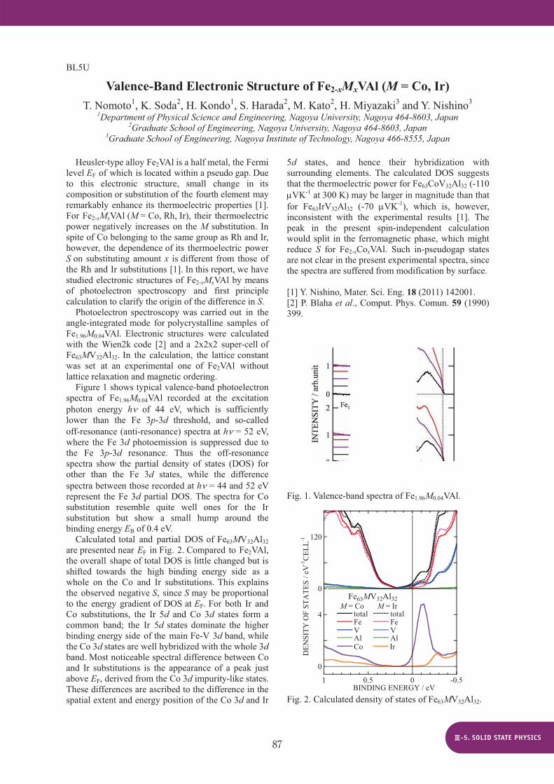
Figure 1 shows typical valence-band photoelectron spectra of Fe1.96M0.04VAl recorded at the excitation photon energy h of 44 eV, which is sufficiently lower than the Fe 3p-3d threshold, and so-called off-resonance (anti-resonance) spectra at h = 52 eV, where the Fe 3d photoemission is suppressed due to the Fe 3p-3d resonance. Thus the off-resonance spectra show the partial density of states (DOS) for other than the Fe 3d states, while the difference spectra between those recorded at h = 44 and 52 eV represent the Fe 3d partial DOS. The spectra for Co substitution resemble quite well ones for the Ir substitution but show a small hump around the binding energy EB of 0.4 eV.
Calculated total and partial DOS of Fe63MV32Al32 are presented near EF in Fig. 2. Compared to Fe2VAl, the overall shape of total DOS is little changed but is shifted towards the high binding energy side as a whole on the Co and Ir substitutions. This explains the observed negative S, since S may be proportional to the energy gradient of DOS at EF. For both Ir and Co substitutions, the Ir 5d and Co 3d states form a common band; the Ir 5d states dominate the higher binding energy side of the main Fe-V 3d band, while the Co 3d states are well hybridized with the whole 3d band. Most noticeable spectral difference between Co and Ir substitutions is the appearance of a peak just above EF, derived from the Co 3d impurity-like states. These differences are ascribed to the difference in the spatial extent and energy position of the Co 3d and Ir
5d states, and hence their hybridization with surrounding elements. The calculated DOS suggests that the thermoelectric power for Fe63CoV32Al32 (-110
VK-1 at 300 K) may be larger in magnitude than that for Fe63IrV32Al32 (-70 VK-1), which is, however, inconsistent with the experimental results [1]. The peak in the present spin-independent calculation would split in the ferromagnetic phase, which might reduce S for Fe2-xCoxVAl. Such in-pseudogap states are not clear in the present experimental spectra, since the spectra are suffered from modification by surface. [1] Y. Nishino, Mater. Sci. Eng. 18 (2011) 142001. [2] P. Blaha et al., Comput. Phys. Comun. 59 (1990) 399.
Fig. 1. Valence-band spectra of Fe1.96M0.04VAl.
Fig. 2. Calculated density of states of Fe63MV32Al32.
-0.500.51
Co Ir
totalFeVAl
totalFeVAl
DEN
SITY
OF
STA
TES
/ eV
-1C
ELL-1
BINDING ENERGY / eV
M = CoFe63MV32Al32
M = Ir
0
4
0
120
87

BL5U
Fabrication of Single-Crystalline EuO Thin Films with SrO Buffer Layer H. Momiyama1, H. Miyazaki2, T. Hajiri3, 4, M. Matsunami4, 5, T. Ito3 and S. Kimura4, 5
1Department of Frontier Materials, Nagoya Institute of Technology, Nagoya 466-8555, Japan 2Center for Fostering Young and Innovative Researchers, Nagoya Institute of Technology, Nagoya 466-8555,
Japan 3Graduate School of Engineering, Nagoya University, Nagoya 464-8603, Japan
4UVSOR Facility, Institute for Molecular Science, Okazaki 444-8585, Japan 5School of Physical Sciences, The Graduate University for Advanced Studies (SOKENDAI), Okazaki 444-8585,
Japan
Europium monoxide (EuO), a ferromagnetic semiconductor, with Curie temperature (Tc) of 69 K, is attracting attention due to its anomalous magneto-optical and transport properties [1, 2]. In the case of electron doping, Tc increases to as high as 200 K. Therefore EuO is one of candidate compounds for next-generation spintronics applications such as spinfilter [3, 4]. To growth high quality ultrathin films, it is important to satisfy small lattice mismatch between EuO and substrate or buffer layer. Then we adopt SrO as buffer layer in between EuO thin film and SrTiO3 substrate, as shown in Fig. 1. SrO forms a rock-salt type crystal structure with a lattice constant of 0.5144 nm, which is the same crystal structure and similar lattice constant as EuO (The lattice mismatch between SrO and EuO is 0.3 %). Due to the quite small lattice mismatch, EuO ultrathin films with a few atomic layers are expected to be epitaxially grown on the SrO buffer layer. To check the existence of the impurity, such as Eu2O3 Eu-metal and Eu valence number of the surface of the thin films, we performed photoemission spectroscopy (PES) measurements of the fabricated thin films.
Single-crystalline EuO ultrathin films and SrO buffer layer with thickness of about 2 and 5 nm, respectively, were grown using a molecular beam epitaxy (MBE) method onto 0.05 wt% Nb-doped SrTiO3 (001) single-crystalline substrates. The PES measurements were performed at the beamline BL5U of UVSOR-II combined with the MBE system. The EuO ultrathin films were prepared in the growth chamber and were transferred to a 3D-ARPES chamber under UHV condition.
Figure 2 shows the PES spectra of EuO 2 nm / SrO 5 nm / SrTiO3 [Fig. 2 (a)] and EuO 5 nm / SrTiO3 [Fig. 2(b)] measured at h 38 eV at 10 K. In the case of EuO 2 nm / SrO 5 nm/ SrTiO3 in Fig. 2 (a), only Eu2+ 4f and O2- 2p exist, in spite that the Eu3+ 4f and metallic states originating from Eu2O3 and Eu metal, respectively, are observed in EuO 2 nm / SrTiO3 in Fig. 2(b) [5]. These results suggest that the SrO buffer layer protects the oxygen diffusion from SrTiO3 substrate to the EuO thin film. Due to the quite small lattice mismatch at the interface and protect the oxygen diffusion, we successfully fabricated single crystalline EuO ultrathin films with a few atomic layers. The technique is useful for next generation spintoronics
devices such as a spin filter.
Fig. 1. Atomic structure of EuO (001) thin film with SrO buffer layer onto SrTiO3 substrate. Lattice constant of SrTiO3, SrO and EuO and lattice mismatch between SrTiO3–SrO and SrO–EuO are shown in the figure.
Fig. 2. Photoemission spectra of EuO 2 nm / SrO 5 nm / SrTiO3 (a), EuO 5 nm / SrTiO3 (b) at the temperature of 10 K with the photon energy of 38 eV, respectively.
[1] N. Tsuda et al., Electronic Conduction in Oxides(Springers College) (1976). [2] A. Mauger et al., J. Phys. (paris) 39 (1978) 1125. [3] A. Schmehl et al., Nature Mater. 6 (2007) 882. [4] M. Müller et al., J. Appl. Phys. 105 (2009) 07C917. [5] H. Lee et al., J. Appl. Phys. 102 (2009) 053903.
88

BL5U
Angle-Resolved Photoemission Study on YbPtSb Y. Shimura1, R. Niwa1, T. Ito1, 2, T. Hajiri1, S. Kimura3, 4, M. Matsunami3, 4 and H. S. Suzuki5
1Graduate School of Engineering, Nagoya University, Nagoya 464-8603, Japan 2 Nagoya University Synchrotron Radiation Research Center, Nagoya University, Nagoya 464-8603, Japan
3Editorial Board, UVSOR Facility, Institute for Molecular Science, Okazaki 444-8585, Japan 4School of Physical Sciences, The Graduate University for Advanced Studies (SOKENDAI), Okazaki 444-8585,
Japan 5National Institute for Materials Science, Tsukuba 305-0047, Japan
A topological insulator, whose physical properties
at the bulk of the system are characterized as insulating or semimetal, while those at the surface as an anomalous metal, attracts much attention as a new spintronics device. It becomes central issue to investigate the anomalous metallic surface states, which appears as the linear dispersions intersecting each other between the bulk energy gap (‘so called Dirac-corn’). So far, angle-resolved photoemission spectroscopy (ARPES) plays a dominant role to establish the 3D topological insulating nature and to probe the topology of their surface states especially in the binary Bi-based series of compounds [1].
Recently, half-Heusler ternary compounds XYZ (XY: transition or rare-earth metal, Z: pnictogen) have been expected to be a new platforms for topological quantum phenomena as spintronic utilization with tunable multifunctionalities (superconductivity, magnetism, heavy-fermion etc.), since the ground state changes from topologically trivial (semiconducting) to topologically nontrivial (semimetallic) as the characteristic energy difference between the 6 and 8 energy levels changes from negative to positive by changing combination of X, Y, and Z atoms [2, 3].
Among half-Heusler ternary compounds, YbPtSb with mostly localized Yb3+ ions [4] might be categorized as a border between the nontrivial and the trivial case as a reference compound LuPtSb. Furthermore, the exceptionally large specific heat coefficient = 8 J/mol K2 as well as a very tiny ordered moment below Tc = 0.4 K has been observed on YbPtSb suggest its additional functionalities due to strong electron correlation effects [5].
In the present study, we have performed ARPES measurements on YbPtSb to clarify the existence of a topologically nontrivial state as well as its relation with extremely heavy carriers.
Figure 1 (a) shows the band structure along the KX symmetry line of YbPtSb obtained by plotting
the intensity of ARPES spectra with h = 30 eV photons. Fig. 1(b) shows the result of LDA band calculation of LuPtSb, referred as the localized Yb3+ ground state, with spin-orbit coupling using the WIEN2k code for comparison. We found that the valence electronic structure around the G point can be qualitatively reproduced by the band calculation though the bandwidth in the experiment seems to be
narrower by twice than the calculation, possibly due to electron correlation effect. On the other hand, we found qualitative discrepancies near the Fermi level. For example, while the calculation on LuPtSb expects only one zero-gap semiconducting nature, two types of Fermi surfaces (FSs), suggesting the semimetallic nature, have been observed by ARPES. One is light FSs at the point and the other is a heavy FS at the X point. Though the origin of the observed differences is not clear yet, one possibility is a sizable hybridization effect of the Yb 4f states with conduction electrons. To elucidate the character of the observed FSs as well as the symmetry of the energy dispersions, further studies using polarization dependent ARPES and systematic studies on LuPtSb are intended.
Fig. 1. (a) ARPES image along the KX symmetry line. White lines are guide for eyes. (b) Band structure calculation of LuPtSb. [1] For example, M. Z. Hasan and C. L. Kane, Rev. Mod. Phys. 82 (2010) 3045. [2] S. Chadov et al., Nature Mat. 9 (2010) 541. [3] H. Lin et al., Nature Mat. 9 (2010) 546. [4] T. Koyama et al., J. Phys. Soc. Jpn. 80 (2011) SA097. [5] Y. Nakanishi et al., Phys. Status Solidi B 247 (2010) 754.
89

BL5U
Temperature Dependent Photoemission Spectra of CaCu3Ti4O12 H. J. Im1, T. Sakurada1, M. Tsunekawa2, K. Kawata1, T. Watanabe1, H. Miyazaki3 and
S. Kimura4, 5 1Department of Advanced Physics, Hirosaki University, Hirosaki 036-8561, Japan
2Faculty of Education, Shiga University, Shiga 522-8522, Japan 3Department of Environmental and Materials Engineering, Nagoya Institute of Technology, Japan
4UVSOR Facility, Institute for Molecular Science, Okazaki 444-8585, Japan 5School of Physical Sciences, The Graduate University for Advanced Studies, Okazaki 444-8585, Japan
A-site ordered perovskite CaCu3Ti4O12 (CCTO) has been attracted much attention due to an extremely high dielectric constant ( ) and its intriguing properties [1]. Particularly, the temperature dependence of physical properties has been of interest. For example, the absence of any structural phase transition around the temperature of 100 K, where the high dramatically drops, is quite a different point with the typical perovskites, the so-called ferroelectrics, where the crystal structural phase transition usually causes the large change of . In addition, the electrical resistivity measurements have showed the variable range hopping conductivity in the insulator phase below about 150 K. To clarify the mechanism of such unusual physical properties, we have carried out the temperature dependent photoemission (PES) experiments on a single crystal CCTO.
PES measurements have performed at BL5U. The used photon energy is 90 eV. The sample surface in the (100) plane was prepared by cleaving in situ in the ultra-high vacuum. The measurement temperatures are from 150 to 300 K. A wide acceptable angle-integrated mode ( 16 ) was used to accumulate the data. The Fermi level was referred to that of gold thin film electrically connected with the sample. In PES experiments of an insulator sample, one should take care of the possibility of charging in the sample during measurement. Therefore, we have investigated the intrinsic properties of CCTO by comparing with spectra obtained by controlling the photon flux with the slit size of the beamline.
Figure 1 (a) shows PES spectra in valence band regime at hv = 90 eV and T = 300 K with various slit sizes. The mainly Cu 3d peak is observed around 4 eV with intense intensity. The broad peak of mainly O 2p states is observed around 5 - 8 eV. Small broad shoulder of mainly Cu 3d – O 2p hybridized states is observed around 2 eV as in our previous results [2]. It is found that the whole shapes of spectra are almost the same in the various slit sizes. However, the small shift of Cu 3d peak is observed in the slit sizes larger than 70 70 m2. We recognize that the typical behavior of the charging is the decease of the intensity of 2 eV peak with increasing the photon flux as shown in the inset of Fig. 1 (a). This can be a good standard point in analyzing the PES spectra.
Figure 1 (b) is the plot of temperature dependent
PES spectra in the valence band regime at hv = 90 eV with the slit size of 30 30 m2 where the sample is not charged up safely as in the above photon flux dependent PES experiments. We find that the whole spectra shapes are almost the same over whole temperature. There is a small shift of Cu 3d peak around 4 eV to the higher binding energy with decreasing the temperature. And the PES spectra reveal that the intensity of Cu 3d – O 2p hybridized states around 2 eV increases with decreasing the temperature, particularly below T = 200 K. This is completely the opposite behavior to the typical case of the charging, indicating the intrinsic property of CCTO. It should be also noted that this temperature is roughly consistent with the temperature where the type of the transport property is changed as mentioned above. The physical meaning and the relation with the high are not clear yet and should be studied further.
Fig. 1. (a) Photon-flux dependent and temperature dependent photoemission spectra of CaCu3Ti4O12 in the valence band regime, obtained with the photon energy of 90 eV. [1] M. A. Subramanian et al., J. Solid State Chem. 151 (2000) 323. [2] H. J. Im et al., UVSOR Activity Report 38 (2011) 87.
90
BL6B
Electric Field Effect on Superionic Conductor T. Awano
Department of Electronic Engineering, Tohoku Gakuin University, Tagajo 985-8537, Japan
Ionic conductivity of superionic conductors is as large as those in liquids. Movement of ions in superionic conductors is not in phase bout random as in liquids. However, existence of correlative movement of conduction ions by Coulomb repulsive interaction has been expected for a long time. Recently calculation simulation has been showing attractive interaction between conduction ions by electronic effect. Low energy spectral characteristics indicate such collective motion of conducting ions[1,2]. If coherent excitation of ionic movement occurs by coherent external electric field, ionic conductivity seems to increase drastically. In this study, I have investigated far-infrared and millimeter wave spectra of superionic conducting crystal RbAg4I5in external electric field.
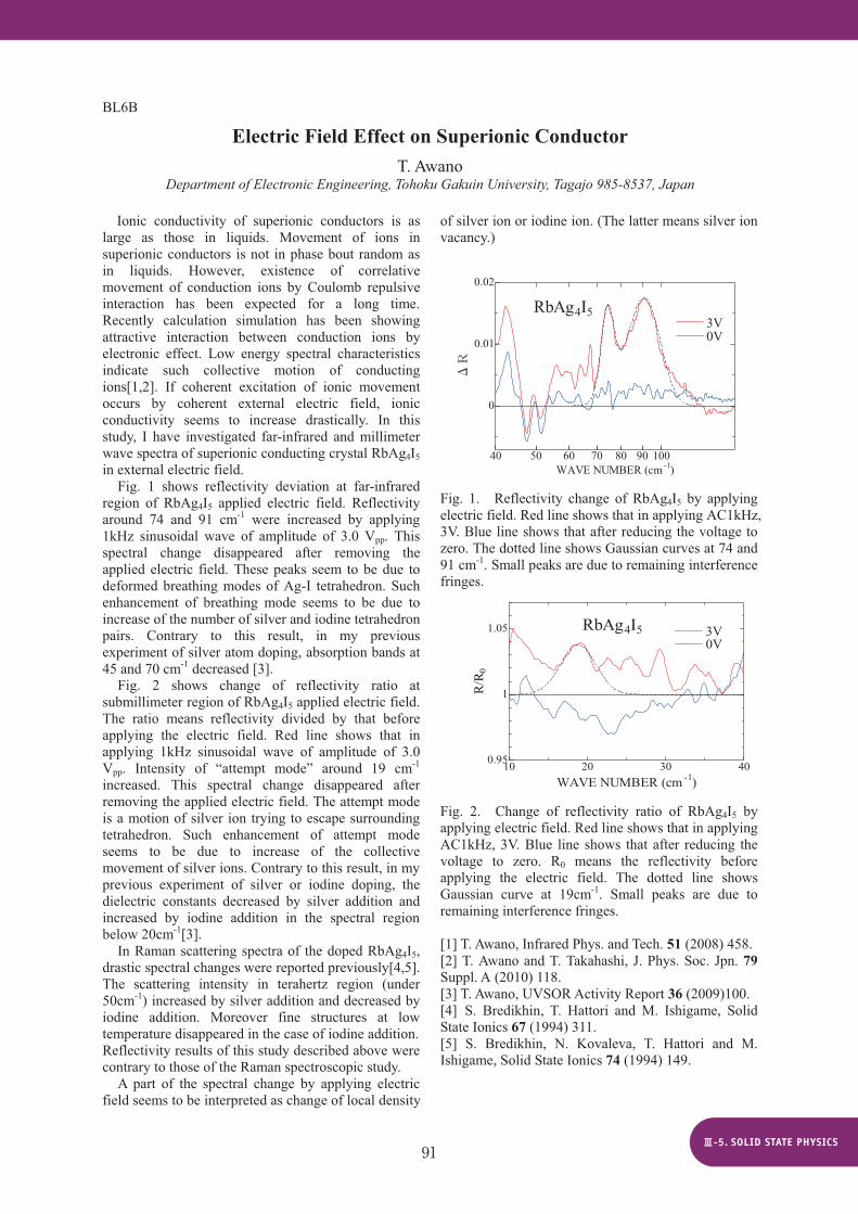
Fig. 1 shows reflectivity deviation at far-infrared region of RbAg4I5 applied electric field. Reflectivity around 74 and 91 cm-1 were increased by applying 1kHz sinusoidal wave of amplitude of 3.0 Vpp. This spectral change disappeared after removing the applied electric field. These peaks seem to be due to deformed breathing modes of Ag-I tetrahedron. Such enhancement of breathing mode seems to be due to increase of the number of silver and iodine tetrahedron pairs. Contrary to this result, in my previous experiment of silver atom doping, absorption bands at 45 and 70 cm-1 decreased [3].
Fig. 2 shows change of reflectivity ratio at submillimeter region of RbAg4I5 applied electric field. The ratio means reflectivity divided by that before applying the electric field. Red line shows that in applying 1kHz sinusoidal wave of amplitude of 3.0 Vpp. Intensity of “attempt mode” around 19 cm-1
increased. This spectral change disappeared after removing the applied electric field. The attempt mode is a motion of silver ion trying to escape surrounding tetrahedron. Such enhancement of attempt mode seems to be due to increase of the collective movement of silver ions. Contrary to this result, in my previous experiment of silver or iodine doping, the dielectric constants decreased by silver addition and increased by iodine addition in the spectral region below 20cm-1[3].
In Raman scattering spectra of the doped RbAg4I5,drastic spectral changes were reported previously[4,5]. The scattering intensity in terahertz region (under 50cm-1) increased by silver addition and decreased by iodine addition. Moreover fine structures at low temperature disappeared in the case of iodine addition. Reflectivity results of this study described above were contrary to those of the Raman spectroscopic study.
A part of the spectral change by applying electric field seems to be interpreted as change of local density
of silver ion or iodine ion. (The latter means silver ion vacancy.)
40 50 60 70 80 90 100
0
0.01
0.02
WAVE NUMBER (cm-1)
RbAg4I5 3V 0V
Fig. 1. Reflectivity change of RbAg4I5 by applying electric field. Red line shows that in applying AC1kHz, 3V. Blue line shows that after reducing the voltage to zero. The dotted line shows Gaussian curves at 74 and 91 cm-1. Small peaks are due to remaining interference fringes.
10 20 30 400.95
1
1.05 RbAg4I5 3V 0V
WAVE NUMBER (cm -1)
R/R
0
Fig. 2. Change of reflectivity ratio of RbAg4I5 by applying electric field. Red line shows that in applying AC1kHz, 3V. Blue line shows that after reducing the voltage to zero. R0 means the reflectivity before applying the electric field. The dotted line shows Gaussian curve at 19cm-1. Small peaks are due to remaining interference fringes.
[1] T. Awano, Infrared Phys. and Tech. 51 (2008) 458. [2] T. Awano and T. Takahashi, J. Phys. Soc. Jpn. 79Suppl. A (2010) 118. [3] T. Awano, UVSOR Activity Report 36 (2009)100. [4] S. Bredikhin, T. Hattori and M. Ishigame, Solid State Ionics 67 (1994) 311. [5] S. Bredikhin, N. Kovaleva, T. Hattori and M. Ishigame, Solid State Ionics 74 (1994) 149.
91

BL7U
Temperature Dependences of Electronic Structure and Chemical Potential of FeSb2
T. Takeuchi1, 2, 3, 4 and T. Shimada41EcoTopia Science Institute, Nagoya University, Nagoya 464-8603, Japan
2Department of Crystalline Materials Science, Nagoya University, Nagoya 464-8603, Japan 3PRESTO, Japan Science and Technology Agency, Saitama 332- 0012, Japan
4Department of Applied Physics, Nagoya University, 464-8603, Japan
FeSb2 is known to possess an extremely large magnitude of Seebeck coefficient reaching -40 mV/K, which is 200 times larger than that of practical thermoelectric materials [1]. The mechanism leading to this huge Seebeck coefficient has not been well understood yet. Therefore, in this study, by emoplying high-resolution angle resolved photoemission spectroscopy (ARPES), we investigated the characteristics of electronic structure near the chemical potential because it is the main factor to determine the electron transport properties including Seebeck coefficient. Single grained FeSb2 samples were grown in the Sb-flux, and we succeeded in obtaining FeSb2 singlecrystals of ~1x1x1 mm3 in dimension. The sample possesses a large evolution of Seebeck coefficient at around 10~30 K as it was reported previously, though the magnitude of Seebeck coefficient is slightly smaller than the reported value. ARPES measurements were conducted at BL7U of UVSOR using photon energy of 22 eV. This photon energy was selected so as the measurable momentum area to cover the whole first Brillouin zone. The orientation of samples were determined by taking Laue pictures, and the clean surface was prepared by cleaving samples in the ultra high vacuum chamber of APRES apparatus just before the measurement. Figure 1 shows temperature dependence of EDC spectrum measured at point. The peak intensity and spectrum weight increases with decreasing temperature, and it becomes evident especially at low temperatures where the large magnitude of Seebeck coefficient is observable. Since the peak was located at the energy 200 meV below the chemical potential, it is naturally understood that the evolution of the peak in measured EDC cannot contribute the increasing magnitude of Seebeck coefficient. The observed evolution of peak suggests the presence of the similar increase of peak intensity near the chemical potential in the conduction band to cause the large increase in the magnitude of Seebeck coefficient with negative sign. In such a case, the chemical potential must possess drastic variation with temperature in the same manner as the significant variation of Seebeck coefficient. Thus, in the next step, we focused on the chemical potential shift. The temperature dependence of chemical potential
(T ) F estimated from the peak energy in EDC was plotted in Fig.2 (a). We also plotted the
contribution of chemical potential on Seebeck coefficient, ( (T ) F ) / ( e T ) [2], together with the measured Seebck coefficient in Fig. 2 (b). The temperature dependence of ( (T ) F ) / ( e T ) shows extremely good consistency with the measured value. This fact unambiguously indicates that the large magnitude of Seebeck coefficient is brought about by the electronic structure effect rather than the phonon-drag effect.
Fig. 1. (a) ARPES intensity I(k, ) of FeSb2
measured at 13 K near the point. The energy distribution curves I ( , ) measured at various temperatures are shown in (b). Evolution of the Peak intensity is observable with decreasing temperature especially below 30 K, where the magnitude of Seebeck coefficient increases.
-0.22
-0.21
Peak
ene
rguy
, pe
ak /
eV
150100500Temperature, T / K
(a)
-600
-400
-200
0
Seeb
ck c
oeff
icie
nt, S
(T) /
V
K-1
150100500Temperature, T / K
(b)
Fig. 2. Temperature dependence of (a) peak energy, (b) Seebeck coefficient and ( (T ) F ) / ( e T ) . The peak energy at 0 K is assumed to be 0.219 meV. The characteristic temperature dependence of Seebeck coefficient was clearly reproduced by that calculated from the chemical potential shift.
[1] A. Bentien, et al., EPL 80 (2007) 17008. [2] T. Takeuchi et al., Mat. Trans. 51 (2010) 421.
92

BL7U
Observation of Anomalous Peaks in the Photoelectron Spectra of Highly Oriented Pyrolytic Graphite: Folding of the Band due to the Surface
Charge Density Wave Transition S. Tanaka1, M. Matsunami2,3 and S. Kimura2,3
1The Insititue of Scientific and Industrial Research, Osaka University, Mihogaoka, Ibaraki 567-0047, Japan 2UVSOR Facility, Institute for Molecular Science, Okazaki 444-8585, Japan
2School of Physical Sciences, The Graduate University for Advanced Studies, Okazaki 444-8585, Japan
Graphite has been regarded as a “textbook” system for solid state physics for many years because of its unique characteristics. In this study, the angle-resolved photoelectron spectroscopy (ARPES) with low-photon energy (7-16eV) is used for the investigation of HOPG (Highly Oriented Pyrolytic Graphite) at a low temperature. We observed for the first time peaks in the low binding energy region (from the Fermi level to 0.7 eV) of the surface normal photoelectron spectra at 11K, which disappear above ~30K. Based on the dispersion along both the parallel and normal to the surface, the peaks are ascribed to the emission from the K(H)-point that is backfolded into the -point as a result of the two-dimensional superperiodicity. The surface charge density wave (CDW) transition is proposed for the driving mechanism of the superperiodicity based on the temperature-dependence of the photoelectron intensity[1].
The ARPES experiments were carried out at the BL7U SAMRAI of the UVSOR-II. Figure (a) shows a series of normal-emission photoelectron spectra of HOPG at 11K using the photon energies from 7.3 to 16eV (0.3eV-step). A distinct peak just below the Fermi level and a smaller peak at the binding energy (EB) ~0.7eV are visible when the photon energy is near 11.5eV with a relatively high intensity. In the normal emission, only the electron states along the
-A line of the Brillouin zone (BZ) can be observed. Therefore, the peaks at EB~0eV and 0.7eV in the ARPES spectra [Fig. (a)] are paradoxical since the
-band of the graphite crosses EF near the K-point, and no corresponding bands near EF have been reported at the center of the BZ.
In order to obtain the information about the two anomalous peaks, we measured the band dispersion by using ARPES at 11K. In Fig. (b), the dispersions of these peaks as a function of k// (inverse vector parallel to the surface) are displayed. The color map shows photoelectron intensity taken at h =13eV. The dispersions of the two peaks closely resemble those of the -bands around the K-point in the graphite. According to the photon-energy dependence of the surface normal photoelectron emission, it is also shown that the dispersion of these peaks along the kz(surface normal) direction is similar to that along the K-H line. Therefore, these peaks cannot be assigned to the defect, edge, or surface states, but are
unambiguously ascribed to the electron emission from the -band at the K(H)-point of the graphite. Then, we can conclude that the K-point of HOPG at 11K is backfolded into the -point as a result of the formation of the 3033 Rp or larger superperiodicity. The detection of the photoelectron emission from the K-point at the surface normal can be provided by the diffraction (scattering) by the reciprocal lattice vector of the 2D superlattice.
We measured the sample-temperature dependence of the photoelectron spectra in order to reveal the condition for the superperiodicity formation. In Fig. (c), the photoelectron intensity at EB=0.016eV (solid circles) in the surface normal PES at h =11.5eV is plotted as a function of the reduced temperature (divided by the critical temperature TC=29K). This temperature-dependence is very similar to that of the X-ray reflection intensity of some materials corresponding to the superlattice formation as a result of the charge density wave (CDW) transition, which is well described with the square of the order-parameter predicted by the BCS-law (solid line). Consequently, it is strongly suggested that the formation of the superlattice in HOPG is caused by the CDW transition. This observation demonstrates the advantage of the photoelectron spectroscopy with the tunable photons of the low energy.
[1] S. Tanaka, M. Matsunami and S. Kimura, Phys. Rev. B 84 (2011) 121411 (R) .
93

BL7U
Three-Dimensional Fermi Surface of YbAl2 Studied by Angle-Resolved Photoemission Spectroscopy
M. Matsunami1, 2, T. Hajiri1, H. Miyazaki1, M. Kosaka3 and S. Kimura1, 2 1UVSOR Facility, Institute for Molecular Science, Okazaki 444-8585, Japan
2School of Physical Sciences, The Graduate University for Advanced Studies (SOKENDAI), Okazaki 444-8585, Japan
3Graduate School of Science and Engineering, Saitama University, Saitama 338-8570, Japan
The topology of the Fermi surface (FS) in the heavy-fermion systems directly reflects the degree of the hybridization between conduction band and 4f state (c-f hybridization) as a key concept for describing the heavy-fermion nature. Angle-resolved photoemission spectroscopy (ARPES) is a powerful tool to probe the c-f hybridized electronic structures. However, most of ARPES measurements have been performed on the basis of the surface Brillouin zone or by using the 4d-4f resonant process, in which the kz dependence of the electronic structure and FS are ignored. Since the heavy-fermion systems generally have three-dimensional electronic structure and FS, ARPES measurements should be done along the bulk Brillouin zone. YbAl2, which crystallizes in the cubic Laves
MgCu2 structure, is a prototypical valence fluctuation system. The Yb mean valence has been estimated to be ~ +2.2 by the hard x-ray photoemission spectroscopy [1]. It strongly suggests that a strong c-f hybridization effect can be realized in YbAl2. Hence YbAl2 is well-suited system for studying the c-f hybridized electronic structures and the FS, particularly in comparison with the band structure calculations. In this work, we have performed a three
dimensional mapping of the FS for YbAl2 by means of ARPES. The ARPES experiment was carried out at the undulator beamline BL7U "SAMRAI" in UVSOR-II [2]. The crystal orientation was determined by Laue x-ray diffraction. The single crystals of YbAl2, which were grown by the Lithium flux method, were cleaved in situ along the (111) plane. The LDA band structure calculations were performed using the WIEN2k code. Figure 1 (a) shows the bulk Brillouin zone of YbAl2. Comparing the photon-energy dependence (16-29 eV) of ARPES data leading to the FS in the kx-kz plane with the LDA calculations as shown in Fig. 1 (b), the inner potential in this system was estimated to be 13.7 eV. Thus, the photon energy of h = 20 eV are chosen so as to obtain the FS in the kx-ky plane as shown in Fig. 1 (c). Two FSs around point in both the kx-kz and the kx-ky planes are well described by the LDA calculations. The results suggest the small renormalization effect in YbAl2, which can be provided by the strong c-f hybridization, consistent with the extremely high Kondo temperature (above 2000 K).
Fig. 1. (a) Brillouin zone of YbAl2, in which the kz corresponds to the (111) direction of the fcc Brillouin zone. (b) and (c) Fermi-surface (FS) mapping of YbAl2 in the kx-kz plane and the kx-ky plane, respectively. The green dots and lines indicate the FSs obtained by the LDA band structure calculations. [1] M. Matsunami et al., J. Phys. Soc. Jpn. 81 (2012) 073702. [2] S. Kimura et al., Rev. Sci. Instrum. 81 (2010) 053104.
(b)
(c)
3.5
3.0
2.5
2.0
k z (Å
-1)
-1.0 -0.5 0.0 0.5 1.0
h = 29 eV
20 eV16 eV
(a)
-0.5
0.0
0.5
k y (Å
-1)
-1.0 -0.5 0.0 0.5 1.0kx (Å
-1)
h = 20 eV
W
Kkx ky
kz
LX
94
BL7U
The Orbital Characters of Low-Energy Electronic Structure in the Iron-Chalcogenide Superconductor KxFe2-ySe2
F. Chen1, Q. Q. Ge1, M. Xu1, Y. Zhang1, X. P. Shen1, M. Matsunami2, S. Kimura2 and D. L. Feng1
1State Key Laboratory of Surface Physics, Department of Physics, and Advanced Materials Laboratory, Fudan University, Shanghai 200433, People’s Republic of China
2UVSOR Facility, Institute for Molecular Science, Okazaki 444-8585, Japan
The newly discovered KxFe2-ySe2 superconductor exhibits many distinct properties from other iron-based superconductor [1], such as its parent compound and electronic structure [2, 3]. Since the electronic structures of iron-based superconductors are dominated by multiple 3d orbitals [4, 5], to understand the unique properties of KxFe2-ySe2, one needs to understand its orbital characters.
The intrinsic phase separation in KxFe2-ySe2 superconductor leads to relatively lower concentration of superconducting phase compared to other iron-based superconductors, however, the strong photon intensity and variable polarizations of beamline BL7U at the ultraviolet synchrotron orbital radiation facility (UVSOR) enable us to successfully resolve the orbital characters of low-energy electronic structure.
Fig. 1. The polarization-dependent APRES data around Z taken with 30 eV photon. (a) The photoemission spectra and their corresponding second derivatives with respect to energy taken in the s and p geometries, respectively, along Z-A direction. (b) is the same as panel a, but taken along Z-R direction.
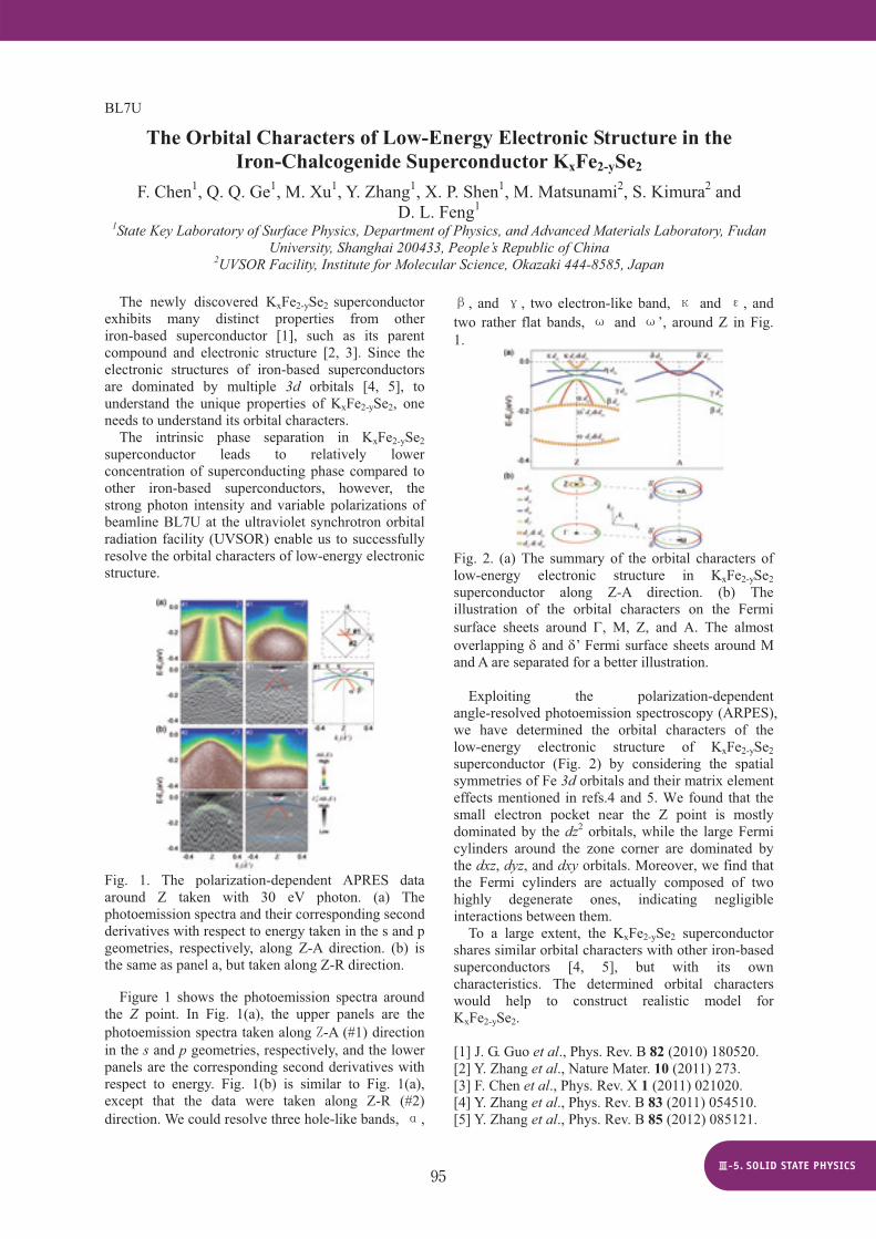
Figure 1 shows the photoemission spectra around the Z point. In Fig. 1(a), the upper panels are the photoemission spectra taken along -A (#1) direction in the s and p geometries, respectively, and the lower panels are the corresponding second derivatives with respect to energy. Fig. 1(b) is similar to Fig. 1(a), except that the data were taken along Z-R (#2) direction. We could resolve three hole-like bands, ,
, and , two electron-like band, and , and two rather flat bands, and ’, around Z in Fig. 1.
Fig. 2. (a) The summary of the orbital characters of low-energy electronic structure in KxFe2-ySe2 superconductor along Z-A direction. (b) The illustration of the orbital characters on the Fermi surface sheets around , M, Z, and A. The almost overlapping and ’ Fermi surface sheets around M and A are separated for a better illustration.
Exploiting the polarization-dependent
angle-resolved photoemission spectroscopy (ARPES), we have determined the orbital characters of the low-energy electronic structure of KxFe2-ySe2 superconductor (Fig. 2) by considering the spatial symmetries of Fe 3d orbitals and their matrix element effects mentioned in refs.4 and 5. We found that the small electron pocket near the Z point is mostly dominated by the dz2 orbitals, while the large Fermi cylinders around the zone corner are dominated by the dxz, dyz, and dxy orbitals. Moreover, we find that the Fermi cylinders are actually composed of two highly degenerate ones, indicating negligible interactions between them.
To a large extent, the KxFe2-ySe2 superconductor shares similar orbital characters with other iron-based superconductors [4, 5], but with its own characteristics. The determined orbital characters would help to construct realistic model for KxFe2-ySe2. [1] J. G. Guo et al., Phys. Rev. B 82 (2010) 180520. [2] Y. Zhang et al., Nature Mater. 10 (2011) 273. [3] F. Chen et al., Phys. Rev. X 1 (2011) 021020. [4] Y. Zhang et al., Phys. Rev. B 83 (2011) 054510. [5] Y. Zhang et al., Phys. Rev. B 85 (2012) 085121.
95

BL7U
Angle-Resolved Photoemission Study on Non-Superconducting Li1+xFeAs T. Hajiri1,2, T. Ito1,3, R. Niwa1 , S. Hirate1, M. Matsunami2,4, B. H. Min5, Y. S. Kwon5 and
S. Kimura2,4 1Graduate School of Engineering, Nagoya University, Nagoya 464-8603, Japan
2UVSOR Facility, Institute for Molecular Science, Okazaki 444-8585, Japan 3Nagoya University Synchrotron radiation Research Center, Nagoya University, Nagoya, 464-8603, Japan
4School of Physical Sciences, The Graduate University for Advanced Studies (SOKENDAI), Okazaki 444-8585, Japan
5 Department of Emerging Materials Science, DGIST, Daegu 711-873, Republic of Korea
LiFeAs is an intriguing iron pnictide superconduc-tor because it shows superconductivity (TC = 18 K) without any structural and SDW/AFM transitions [1]. In pristine LiFeAs, we have demonstrated that the electronic structure can be fundamentally explained by a LDA band structure calculation. We have also pointed out the importance of the interband scattering between hole and electron Fermi surfaces in terms of the appearance of superconductivity [2]. In this sys-tem, the excess or deficiency of Li-ions from the stoichiometry has been reported to suppress the su-perconductivity [3] and enlarges spin fluctuation [4]. However, the reason of the suppression of the super-conductivity owing to the off-stoichiometry has not been clarified yet.
To elucidate the effect of the Li excess or defi-ciency to the electronic structure, we performed a polarization-dependent three-dimensional an-gle-resolved photoemission spectroscopy (3D-ARPES) of a Li-excess LiFeAs (Li1+xFeAs) without superconducting transition at BL7U, UVSOR-II. Figure 1 shows a normal emission (k = 0 Å-1) AR-PES image of Li1+xFeAs measured at T = 12 K along the Z-A direction. The blue line indicates the trace of the peak positions of the momentum distribution curves (MDCs) and the green dashed lines indicate the dispersion curves derived from an LDA band cal-culation. The obtained band dispersion is strongly renormalized below 100 meV. The renormalized bare band is assumed as the green solid line in Fig. 1. The obtained band dispersion has kink structure that is away from the assumed bare band at about 20 meV and 100 meV. In order to argue about the kink structure qualita-tively, we performed the self-energy analysis. Figure 2 shows the real part of the self-energy Re ( ), which is obtained by the subtraction of the assumed bare band dispersion from the MDC dispersion. The Re ( ) spectrum clearly has two peaks; one is lo-cated at about 20 meV and the other at about 100 meV. The former is consistent with phonon energy position as shown by the dashed lines reported by Raman spectroscopy [5] and theory [6]. However, the later peak cannot be explained by the phonon origin. A recent inelastic neutron scattering (INS) study in-dicated that the spin excitation peak appears at around
100 meV as shown by a blue line [7], which is con-sistent with the observed higher-energy kink. This suggests that the higher-energy kink originates from magnetic excitations.
Fig. 1. ARPES image of Li1+xFeAs measured at T = 12 K along the Z-A direction.
Fig. 2. The real part of the self-energy Re ( ) indi-cated by a red solid line. Vertical dashed lines indi-cate the phonon energy position [5, 6] and blue line indicates the energy dependence of the local suscep-tibility of Li0.94FeAs obtained by INS [7]. [1] X. C. Wang et al., Solid State Commun. 148 (2008) 538. [2] T. Hajiri et al., Phys. Rev. B 85 (2012) 094509. [3] M. Wang et al., Phys. Rev. B 83 (2011) 220515(R). [4] L. Ma et al., Phys. Rev. B 82 (2010) 180501(R). [5] Y. J. Um et al., arXiv:1109.5797. [6] R. A. Jishi et al., Adv. Condens. Matter Phys. 2010 (2010) 804343. [7] M. Wang et al., Phys. Rev. B 83 (2011) 220515(R).
96
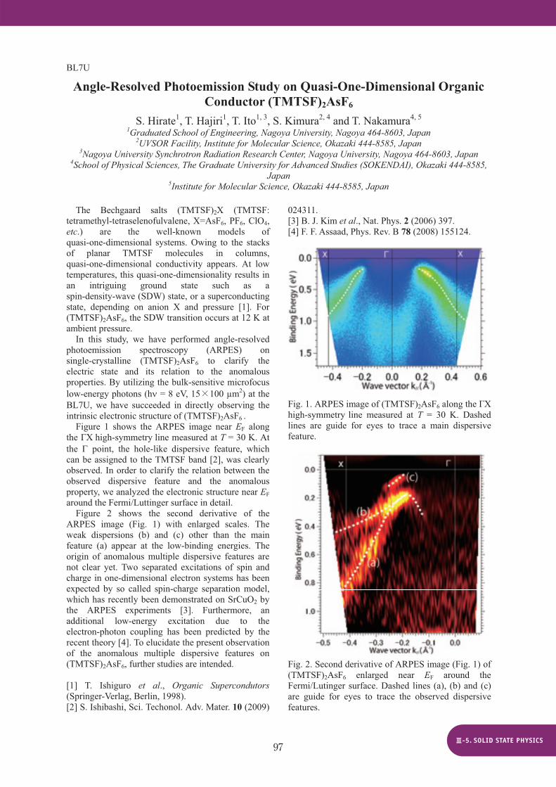
BL7U
Angle-Resolved Photoemission Study on Quasi-One-Dimensional Organic Conductor (TMTSF)2AsF6
S. Hirate1, T. Hajiri1, T. Ito1, 3, S. Kimura2, 4 and T. Nakamura4, 5 1Graduated School of Engineering, Nagoya University, Nagoya 464-8603, Japan
2UVSOR Facility, Institute for Molecular Science, Okazaki 444-8585, Japan 3Nagoya University Synchrotron Radiation Research Center, Nagoya University, Nagoya 464-8603, Japan
4School of Physical Sciences, The Graduate University for Advanced Studies (SOKENDAI), Okazaki 444-8585, Japan
5Institute for Molecular Science, Okazaki 444-8585, Japan
The Bechgaard salts (TMTSF)2X (TMTSF: tetramethyl-tetraselenofulvalene, X=AsF6, PF6, ClO4, etc.) are the well-known models of quasi-one-dimensional systems. Owing to the stacks of planar TMTSF molecules in columns, quasi-one-dimensional conductivity appears. At low temperatures, this quasi-one-dimensionality results in an intriguing ground state such as a spin-density-wave (SDW) state, or a superconducting state, depending on anion X and pressure [1]. For (TMTSF)2AsF6, the SDW transition occurs at 12 K at ambient pressure.
In this study, we have performed angle-resolved photoemission spectroscopy (ARPES) on single-crystalline (TMTSF)2AsF6 to clarify the electric state and its relation to the anomalous properties. By utilizing the bulk-sensitive microfocus low-energy photons (h = 8 eV, 15 100 μm2) at the BL7U, we have succeeded in directly observing the intrinsic electronic structure of (TMTSF)2AsF6 .
Figure 1 shows the ARPES image near EF along the X high-symmetry line measured at T = 30 K. At the point, the hole-like dispersive feature, which can be assigned to the TMTSF band [2], was clearly observed. In order to clarify the relation between the observed dispersive feature and the anomalous property, we analyzed the electronic structure near EF around the Fermi/Luttinger surface in detail.
Figure 2 shows the second derivative of the ARPES image (Fig. 1) with enlarged scales. The weak dispersions (b) and (c) other than the main feature (a) appear at the low-binding energies. The origin of anomalous multiple dispersive features are not clear yet. Two separated excitations of spin and charge in one-dimensional electron systems has been expected by so called spin-charge separation model, which has recently been demonstrated on SrCuO2 by the ARPES experiments [3]. Furthermore, an additional low-energy excitation due to the electron-photon coupling has been predicted by the recent theory [4]. To elucidate the present observation of the anomalous multiple dispersive features on (TMTSF)2AsF6, further studies are intended. [1] T. Ishiguro et al., Organic Supercondutors (Springer-Verlag, Berlin, 1998). [2] S. Ishibashi, Sci. Techonol. Adv. Mater. 10 (2009)
024311. [3] B. J. Kim et al., Nat. Phys. 2 (2006) 397. [4] F. F. Assaad, Phys. Rev. B 78 (2008) 155124.
Fig. 1. ARPES image of (TMTSF)2AsF6 along the X high-symmetry line measured at T = 30 K. Dashed lines are guide for eyes to trace a main dispersive feature.
Fig. 2. Second derivative of ARPES image (Fig. 1) of (TMTSF)2AsF6 enlarged near EF around the Fermi/Lutinger surface. Dashed lines (a), (b) and (c) are guide for eyes to trace the observed dispersive features.
97

BL7B
Optical Characterization and Computational Chemical Evaluation of Electronic Localized States in Polyolefin
T. Arai1, M. Hosobuchi1, N. Fuse2, K. Takeda1 and Y. Ohki11Waseda University, 3-4-1 Ohkubo, Shinjuku-ku, Tokyo 169-8555, Japan
2Central Research Institute of Electric Power Industry, 2-6-1 Nagasaka, Yokosuka-shi, Kanagawa 240-0196, Japan
Optical absorption spectra and photoluminescence spectra were obtained for eight kinds of polyolefin sheet samples using photons in a range from visible to vacuum ultraviolet. Almost all samples were found to exhibit an absorption peak at around 6.5 eV and a luminescence band at around 4.3 eV as shown in Figs. 1 and 2. The luminescence was found to be induced by the absorption. Furthermore, it was found that successive absorption of ultraviolet photons weakens the luminescence intensity [1, 2]. It is assumed from these results that , -unsaturated carbonyls are luminous and that the carbonyls are decomposed through the Norrish type II reaction by absorbing ultraviolet photons [3, 4]. In Norrish type II reaction,
-unsaturated carbonyls change to -unsaturatedcarbonyls, which are then separated into pure carbon double bonds and pure carbonyls by main chain scissions.
Quantum chemical calculations were carried out using polyethylene models with and without an unsaturated carbonyl to verify the above-mentioned assumption. From the calculation results, the model with an unsaturated carbonyl was found to have localized electronic states in the forbidden band as shown in Fig. 3. One of the differential energies between the states is close to the photon energy, by which the luminescence is induced. The bond length of a double bond, which is next to the carbonyl, was found to be longer at the excited singlet state than at the ground state. These results obtained by the quantum chemical calculations support the above-mentioned assumption of the luminescence center and its decomposition.
[1] T. Ito et al., IEEJ Trans. FM 121 (2001) 865 (in Japanese). [2] T. Ito, N. Fuse and Y. Ohki, IEEJ Trans. FM 124(2004) 624. [3] N. S. Allen, J. Homer and J. F. McKellar, J. Appl. Polym. Sci. 21 (1977) 2261. [4] N. S. Allen and J. F. McKellar, J. Appl. Polym. Sci. 22 (1978) 3277.
2 3 4 5 6 7 80
500
1000
1500
Photon Energy (eV)
Abs
orpt
ion
Coe
ffic
ient
(cm
-1)
PE (30 m) PP (46 m) PMP (50 m)
Fig. 1. Absorption spectra measured by vacuum ultraviolet spectroscopy observed for PE, PP and PMP. The numerals in parentheses are the thicknesses of the samples.
Detected Photon Energy (eV)
PL In
tens
ity (a
.u.)
0.2
0
0.4
0.6
0.8
17
6
5
4
6.5
5.5
4.5
2 3 4 54.53.52.5
Exci
tatio
n Ph
oton
Ene
rgy
(eV
)
(a) PE
Detected Photon Energy (eV)
PL In
tens
ity (a
.u.)
0.2
0
0.4
0.6
0.8
17
6
5
4
6.5
5.5
4.5
2 3 4 54.53.52.5
Exci
tatio
n Ph
oton
Ene
rgy
(eV
)
(b) PP
Fig. 2. Two-dimensional intensity distributions of various PL peaks observed for PE (a) and PP (b) at 10 K.
VB
CB
VB
CB
D3 pp
D2 pp
D1 pp *
E(e
V)
D1
C : pyC : py
O : py
(a) C25H52 (b) C25H48O
zx
y
Fig. 3. The energy levels of C25H52 (a) and C25H48O(b).
98
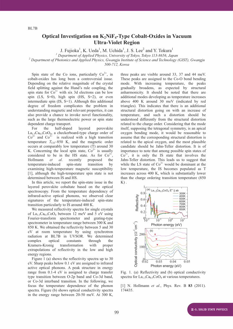
BL7B
Optical Investigation on K2NiF4-Type Cobalt-Oxides in Vacuum Ultra-Violet Region
J. Fujioka1, K. Ueda1, M. Uchida1, J. S. Lee2 and Y. Tokura11 Department of Applied Physics, University of Tokyo, Tokyo 113-8656, Japan
2 Department of Photonics and Applied Physics, Gwangju Institute of Science and Technology (GIST), Gwangju 500-712, Korea
Spin state of the Co ions, particularly Co3+, in cobalt-oxides has long been a controversial issue. Depending on the relative magnitude of the crystal field splitting against the Hund’s rule coupling, the spin state for Co3+ with six 3d electrons can be low spin (LS, S=0), high spin (HS, S=2), or even intermediate spin (IS, S=1). Although this additional degree of freedom complicates the problem in understanding magnetic and relevant properties, it can also provide a chance to invoke novel functionality, such as the large thermoelectric power or spin state dependent charge transport.
For the half-doped layered perovskite La1.5Ca0.5CoO4, a checkerboard-type charge order of Co2+ and Co3+ is realized with a high transition temperature TCO~850 K, and the magnetic order occurs at comparably low temperature (T) around 30 K. Concerning the local spin state, Co2+ is usually considered to be in the HS state. As for Co3+,Hollmann et al. recently proposed the temperature-induced spin-state transition by examining high-temperature magnetic susceptibility [1], although the high-temperature spin state is not determined between IS and HS.
In this article, we report the spin-state issue in the layered perovskite cobaltate based on the optical spectroscopy. From the temperature dependency of infrared-active optical phonons, we observed clear signatures of the temperature-induced spin-state transition particularly to IS around 400 K. We measured reflectivity spectra for single crystals of La1.5Ca0.5CoO4 between 12 meV and 5 eV using Fourier-transform spectrometer and grating-type spectrometer in temperature range between 300 K and 850 K. We obtained the reflectivity between 5 and 30 eV at room temperature by using synchrotron radiation at BL7B in UVSOR. We determined complex optical constants through the Kramers-Kronig transformation with proper extrapolations of reflectivity in the low and high energy regions.
Figure 1 (a) shows the reflectivity spectra up to 30 eV. Sharp peaks below 0.1 eV are assigned to infrared active optical phonons. A peak structure in energy range from 0.1-4 eV is assigned to charge transfer type transition between O-2p band and Co-3d band, or Co-3d interband transition. In the following, we focus the temperature dependence of the phonon spectra. Figure (b) shows optical conductivity spectra in the energy range between 20-50 meV. At 300 K,
three peaks are visible around 33, 37 and 44 meV. These peaks are assigned to the Co-O bond bending mode. With increasing temperature, the peaks gradually broadens, as expected by structural anharmonicity. It should be noted that there are additional modes developing as temperature increases above 400 K around 30 meV (indicated by red triangles). This indicates that there is an additional structural distortion going on with an increase of temperature, and such a distortion should be understood differently from the structural distortion related to the charge order. Considering that the mode itself, supposing the tetragonal symmetry, is an apical oxygen bending mode, it would be reasonable to assume that the corresponding structural distortion is related to the apical oxygen, and the most plausible candidate should be Jahn-Teller distortion. It is of importance to note that among possible spin states of Co3+, it is only the IS state that involves the Jahn-Teller distortion. This leads us to suggest that while the LS state of Co3+ would be dominant at the low temperature, the IS becomes populated as T increases across 400 K, which is substantially lower than the charge ordering transition temperature (850 K) .
Fig. 1. (a) Reflectivity and (b) optical conductivity spectra for La1.5Ca0.5CoO4 at various temperatures.
[1] N. Hollmann et al., Phys. Rev. B 83 (2011). 174435.
10-2 10-1 100 1010
0.2
0.4
0.6
0.8
1
Photon energy (eV)
Ref
lect
ivity
300K 400K 500K 600K 700K 800K 850K
La1.5Ca0.5CoO4 E || ab(a)
0.02 0.03 0.04 0.050
100
200
Photon energy (eV)Opt
ical
con
duct
ivity
(-1
cm-1
)
(b)
99

BL7B
Decay Behaviors of Auger-Free Luminescence in Cs2ZnCl4
A. Ohnishi1, M. Saito1, M. Kitaura1, M. Sasaki1 and M. Itoh21Depeartment of Physics, Yamagata University, Yamagata 990-8560, Japan
2Department of Electrical and Electronic Engineering, Shinshu University, Nagano 380-8553, Japan
The crystal of Cs2ZnCl4 is composed of anionic ZnCl4 tetrahedra separated from each other and interstitial Cs cations between them [1]. In the previous work [2], we have investigated optical properties of Cs2ZnCl4 crystals with the use of synchrotron radiation as a light source, and observed Auger-Free luminescence (AFL) resulting from a radiative transition between the Cl 3p valence band and the Cs 5p outermost core band. In the present study, we have studied decay behaviors of AFL using a time-correlated single-photon counting method under the single bunch operation.
Cs2ZnCl4 crystals were prepared by evaporating a stoichiometric mixture of solutions of CsCl and ZnCl2.Experiments were performed at the BL7B beamline of UVSOR. Luminescence from samples was dispersed by a grating monochromator and detected by a microchannel-plate photomultiplier.
When Cs2ZnCl4 is excited at 10 K at 21.4 eV, three AFL bands peaking at 3.2 4.1 and 4.8 eV are observed. In Fig. 1, decay curves of AFL measured at 3.2, 4.1 and 4.8 eV are shown in semi-logarithmic scale, where decay curves are vertically displaced for comparison. The photo-excitation was made at 21.4 eV at 10 K. Three decay curves are parallel with each other. That is, the decay profile is fundamentally the same for each band. This result suggests that the life time is governed by that of the holes created on the outermost core band. We can see a somewhat fast component in the earlier stage of the decay curves. If we estimate the lifetime from a least-square fit to the single exponential decay by neglecting the component, the decay time is about 2.0 ns. The red straight line drawn on the experimental data of the 3.2 eV AFL shows a single exponential curve with lifetime of 2.0 ns. Figure 2 shows decay behaviors of the 4.1 eV band at 10 and 300 K. The decay time at 300 K is estimated to be 1.6 ns. The decay time is a little shorter than that at 10 K. This temperature dependence was the same for the AFL at 3.2 and 4.8 eV. The life time of AFL is much longer compared to the
lattice relaxation time. Thus, it is probable that the core hole induces some lattice distortion within the life time and interacts with the lattice vibrations. In fact, the AFL spectrum observed was red-shifted than the energy range expected within the rigid band model. Furthermore, the linewidths of AFL bands were found to be gradually broadened as increasing the sample temperature, though the overall structures of AFL spectrum were not very sensitive to the sample temperature between 10 and 300 K. These details will be reported somewhere.
Fig. 1. Decay behaviors of AFL detected at 3.2, 4.1, and 4.8 eV in Cs2ZnCl4.
Fig. 2. Decay behaviors of AFL detected at 4.1 eV at 10 and 300 K in Cs2ZnCl4.
[1] J. A. Mcginnery, Inorg. Chem. 13 (1974) 1057. [2] A. Ohnishi, T. Otomo, M. Kitaura and M. Sasaki, J. Phys. Soc. Jpn. 72 (2003) 2400.
100

BL7B
Electronic Status of Rare-Earth Ion in Glass Host by Characterizing Photoluminescence of Rare-Earth Doped APLF Glass Scintillator
M. Tsuboi1, M. Kouno1, K. Takeda1, T. Nakazato1, T. Shimizu1, M. Cadatal-Raduban1,K. Yamanoi1, K. Sakai1, R. Nishi1, Y. Minami1, Y. Arikawa1, N. Sarukura1, T. Norimatsu1,
M. Nakai1, H. Azeti1, T. Murata2, S. Fujino3, H. Yoshida4, T. Suyama5, K. Fukuda5,A. Yoshikawa6, N. Sato7, H. Kan7 and K. Kamada8
1Inst. Laser Engineering, Osaka Univ. ,2Kumamoto Univ. ,3Kyushu Univ. ,4Ceramic Research Center of Nagasaki, 5Tokuyama Corp. ,6Inst. Materials Research, Tohoku Univ. ,7Hamamatsu Photonics K.K. ,8Furukawa Co., Ltd.
The realization of nuclear fusion is highly expected to satisfy the energy demand in the future. Fusion plasma diagnostics at higher plasma areal density than 3 g/cm2 is one of the biggest breakthrough in nuclear fusion research. Scattered-neutron diagnostics [1] utilizing Pr3+-doped 20Al(PO3)3-80LiF (APLF+Pr) glass scintillator is expected to achieve plasma areal density measurement in fusion core. APLF+Pr, which have high sensitivity for scattered neutrons and fast response time about 5.4 ns, is the key factor of the measure.
In this work, we report the luminescence properties of APLF+Pr at different Pr3+ concentrations (0.5mol% 3mol%).
We have measured Photoluminescence (PL) spectra and Photoluminescence Excitation (PLE) spectra of APLF+Pr at 30K, 50K, 150K, 200K, 250K, and 300K. The experiment was conducted at BL7B utilizing G2 grating. PL spectra are measured with excitation wavelength at 80nm, 120nm, 150nm, 180nm, and 200nm. The APLF+Pr samples, having Pr+ density at 0.5mol%, 1mol%, 2mol%, and 3mol%, and cut into 10 mm 10 mm 10 mm, were prepared. PL and PLE spectra of Pr3+-doped LiCaAlF6 (Pr:LiCAF) was measured as well for comparison.
The PL spectra of APLF+Pr and Pr:LiCAF excited by 180 nm radiation are shown in Fig. 1. The green colored lines are corresponding to spectra of APLF+Pr with Pr3+ density at 0.5mol%, 1mol%, 2mol% and 3mol% and red line to that of Pr:LiCAF. The UV luminescence around 250 nm are observed for each samples.
The PLE spectra of APLF+Pr monitoring 240 nm, 400 nm, and 480 nm are illustrated in Fig. 2. The 240 nm emission is attributed to 4f5d 4f2 transition. In the other hand, the 400 nm emission occurs from both 4f5d and 1S0.
These consequences indicate that 5d state of Pr3+ in APLF glass host vary in wide range as shown in Fig. 3.
[1] M. Moran et al., Rev. Sci. Instrum. 75 (2004) 3592.
Fig. 1. PL spectra of APLF+Pr and Pr:LiCAF.
Fig. 2. PLE spectra of APLF+Pr.
Fig. 3. Energy status of Pr3+ in APLF glass host.
101

BL7B
Vacuum UV Reflectance Spectrum of Diamond H. Okamura
Graduate School of Science, Kobe University, Kobe 657-8501, Japan
Diamond is one of the most familiar and classical materials of all, with its well known crystal structure and the covalent bonding. Accordingly, its band structure has been studied extensively since the early stage of the band calculation technique. To examine the energy dependent band structure of a material, it is very useful to compare the dielectric function
derived from the calculated band structure with that derived from the measured optical spectra. The Kramers- Kronig analysis is often used to derive from a reflectance spectrum R( ) measured over a wide photon energy range.
In spite of the familiarity of this material in the condensed matter and materials physics, experimental studies of its optical properties above the fundamental absorption edge have been only reported by a small number of papers [1-5]. Namely, several papers on the UV and vacuum UV (VUV) reflectance measurements of diamond appeared in the 1960’s, but since then, no further measurements seem to have been reported [6], in spite of the persisting interest from the theoretical point of view [6-8].
In view of the above situation, we have measured the reflectance of diamond in the VUV using the synchrotron radiation source at BL7B of UVSOR. The diamond sample used was a diamond anvil used for high pressure optical experiments in our laboratory at Kobe University. The anvil was of type IIa with low density of impurities, and had a table diameter of 3.1 mm, a culet diameter of 0.4 mm, and a height of 1.7 mm. The light beam was incident on the table side of the diamond. Below the fundamental absorption edge, there may have been reflection from the back (culet) surface, but this should not occur above the absorption edge.
Figure 1 shows the measured reflectance spectrum R( ) of diamond at room temperature. It has a high reflectance band at 12-22 eV and peaks at 7 and 12.5 eV, which had been observed previously [1-5]. The weak structure at 5.5 eV is due to the fundamental absorption edge of diamond. This structure is only weak since the fundamental absorption edge is due to an indirect band gap. The peak at 7 eV is due to the smallest direct band gap, which was studied in detail including its temperature dependence [4]. However, the shoulder at 10 eV and the dip at 23 eV were not clearly observed in the previous works [1-5]. In the old measurements made in the 1960’s, discrete lines from discharge lamps were used as the light source, and then the measured reflectance at the discrete photon energies were interpolated. This resulted in poor spectral resolution, and these structures had probably been overlooked. We plan further
measurements in the future, including the temperature dependences, to make available more complete optical spectra of this important material for comparison with the results of band calculations.
0
0.2
0.4
0.6
0.8
5 10 15 20 25 30
Diamond (type IIa) 300 K
Photon Energy (eV)
Ref
lect
ance
Fig. 1. Reflectance spectrum a type IIa diamond anvil at room temperature. [1] H. R. Philipp and E. A. Taft, Phys. Rev. 127 (1962) 159. [2] W. C. Walker and J. Osantowski, Phys. Rev. 134 (1964) A153. [3] H. R. Philipp and E. A. Taft, Phys. Rev. 136 (1964) A1445. [4] R. A. Roberts, D. M. Roessler and W. C. Walker, Phys. Rev. Lett. 17 (1966) 302. [5] R. A. Roberts and W. C. Walker, Phys. Rev. 161 (1967) 730. [6] V. V. Sobolev, A. P. Timonov and V. Val. Sobolev, Optics and Spectroscopy 88 (2000) 255. [7] A. D. Papadopoulos and E. Anastassakis, Phys. Rev. B 43 (1991) 5090. [8] S. Logothetidis, J. Petalas, H. M. Polatoglou and D. Fuchs, Phys. Rev. B 46 (1992) 4483.
102
BL7B
Photoluminescence - Photoluminescence Excitation Spectra of a-Plane AlN R. Ikematsu, H. Iwai, K. Ozaki and K. Fukui
Fac. Engi., Univ. Fukui, Fukui 910-8507, Japan
The uppermost of the valence band (VB) at the point of the AlN is split into three bands, LH, HH, and CH bands. These splits are due to the crystal-field splitting and the spin-orbit splitting. However, both the crystal-field splitting energy ( cr) and the spin-orbit splitting energy ( so) of the AlN are different from those of the GaN [1]. Then, the uppermost VB ordering at the point of the AlN and GaN are CH-HH-LH (top-to-bottom order) and HH-LH-CH, respectively. The important point is that the transition from CH band, and HH and LH bands to the conduction band (CB) are allowed for E // c and E c, respectively, where E represents the electric field vector of the excitation light and c the crystal axis. It means that it is not easy to measure the minimum bandgap of AlN, because the AlN samples are usually thin films and the c axis are perpendicular to the surfaces (c-plane AlN). On the other hand, the c-axis is parallel to the sample surface in the case of a-plane AlN (See Fig. 1). Then, we can measure the optical anisotropy of AlN by the in-plane rotating. In this report, we present the photoluminescence (PL) - PL excitation (PLE) spectra of the a-plane AlN single crystalline film.
Fig. 1. c-plane (left) and a-plane (right) of the wurtzite AlN
The AlN single crystalline film was grown on the
r-plane sapphire substrate by the MOVPE method [2]. All measurements have been performed at BL7B. The PL from the sample at about 20 K is measured by the conventional 0.3 m monochromator with the Liq. N2 cooled CCD.
Figure 2 shows the PL-PLE spectrum of the a-plane AlN at 20 K with E c (above) and E // c (below) configurations. The horizontal and the vertical axes represent the photon energy of the PL and the excitation energy, respectively. The vertical straight-line like trajectory at 6.05 eV in each configuration represents the well-known PL peak due to the free and bound excitons of the AlN, and are strongly excited at 6.3 – 6.35 eV (red and white
regions) in E c configuration. The white region at the lower photon energy side and the white slant line at the higher photon energy show the impurity PL and Rayleigh scattering of the excitation light, respectively. In the E // c configuration, the PL - PLE spectrum shows at least three slant line like trajectory parallel to that of the Rayleigh scattering. The energy differences among these lines are always 1, 2 or 3 110 meV. Here the photon energy difference, 110 meV, is in good agreement with the LO photon energy of the AlN. Then, we consider that these lines are attributed to the resonance Raman lines.
Fig. 2. The photoluminescence – photoluminescence excitation (PL – PLE) spectra at 20 K of a-plane AlN thin film with E c (above) and E // c (below) configurations.
[1] T. Onuma, S. F. Chichibu, T. Sota, K. Asai, S. Sumiya, T. Shibata and M. Tanaka, Appl. Phys. Lett. 81 (2002) 652. [2] N. Okada, N. Kato, S.Sato, T. Sumii, N. Fujimot, M. Imura, K. Balakrishnan, M. Iwaya, S. Kamiyama, H. Amano, I. Akasaki, T. Noro and A. Bandoh, J. Cryst. Growth 300 (2007) 141.
5.0 5.2 5.4 5.6 5.8 6.0 6.2 6.4 6.6
Low
Photon Energy (eV)
High
Exci
tatio
n En
ergy
(eV)
103
BL7B
Refractive Index of Heavily Boron Doped Diamond with Impurity Band T. Inushima1, Y. Ota1 and K. Fukui2
1Department of Electronics, Tokai University, 4-1-1 Kitakaname, Hiratsuka 259-1292, Japan 2Department of Electrical and Electronics Eng., University of Fukui, Bunkyo, Fukui 910-8507, Japan
Since the discovery of superconductivity in
boron-doped diamond, its impurity band structure has been a key issue for the understanding of the superconductivity. Recently we reported that when the boron concentration exceeds NB=4 1018cm-3, an impurity band forms at the first excited levels (2p) of the impurity boron at 0.06 eV above the valence band maximum. At higher NB, the wave functions of the 2P states begin to overlap and the impurity band spreads in the k-space. Simultaneously, Fermi level rises to the impurity band and a variable range hopping is realized [1]. When the impurity band has k-space dependence, the refractive index should change, especially in the visible region. However, precise refractive index measurement was not been reported. Hence we measure the refractive index of boron doped diamond with impurity band using BL7B and compare it with that obtained by the density functional first principle calculation.
Figure 1 shows the refractive index of 5000 ppm boron doped diamond measured at 300 K by a combination of G3 grating (1.2~7.7 eV) and a photo-diode detector of BL7B. The value of 5,000 ppm corresponds to NB=1 1019cm-3. The reflection spectrum shown in the inset shows weak sinusoidal interference fringes caused by the interference of the transmitting light of the homo-epitaxial diamond film. Using the film thickness of 1.6 m, the refractive index is obtained from the oscillatory order of the interference so as to fit the optimum refractive index of 2.4 at 1.8 eV, where the oscillation disappears. The observed refractive index is much smaller than that of the bulk diamond (n~2.4), and shows a continuous decrease as the photon energy decreases and becomes less than 1 around 1.2 eV.
Figure 2 shows the refractive index of boron doped diamond obtained by ab initio calculation. The used program is Advance/PHASE and the cutoff wavefunction energy is 25 Hartree. The calculation model is the diamond C63B super cell, where the Bravais unit cell of diamond is expanded to 2 2 2 and one carbon atom is replaced by a boron, which corresponds to NB=2.7 cm-3. For comparison, refractive indices of single unit cell diamond and C53B super cell are also plotted. The calculated refractive index is in good agreement with that obtained in Fig. 1, which indicates that the impurity band forming in the boron doped diamond with NB=1 1019cm-3 is similar to that with a boron concentration two orders of magnitude larger.
In conclusion, when the impurity band is established in boron doped diamond when NB>
4 1018cm-3, it has k-space dependence and changes the refractive index in the visible region.
1.0 1.2 1.4 1.6 1.80
1
2
3
500 600 700 800 900 1000 11000.10
0.15
0.20
Ref
lect
ivity
(ar
b. u
nits
)
Wavelength (nm)
Ref
ract
ive
inde
x
Photon energy (eV)
5000 ppm Boron doped diamond
Fig. 1. Refractive index of 5000 ppm boron doped diamond. Inset shows the sinusoidal oscillation of the reflection spectrum caused by interference of the transmitted light.
0 1 2 3 4 50
2
4
6
Ref
ract
ive
inde
x (R
e)
Photon energy (eV)
C2
C63B C53B
0 10 20 30 400
2
4
6
0.994 0.819 0.8533
oscillator stregth per electron
Ref
ract
ive
inde
x (R
e)
Photon energy (eV)
Fig. 2. Refractive indices of diamond, C63B and C58B super cells obtained by ab initio calculations. [1] T. Inushima, R. F. Mamin and H. Shiomi, Phys. Rev. B 79 (2009) 045210.
104

BL8B
Photoelectron Spectroscopy of Sc3N@C78*
S. Hino1, M. Zenki1, T. Zaima1, Y. Aoki1, S. Okita1, T. Ohta1, H. Yagi1, T. Miyazaki1,R. Sumii2, 3, H. Okimoto4, Y. Ito4 and H. Shinohara4
1Graduate School of Science and Engineering, Ehime University, Matsuyama 790-8577, Japan 2UVSOR, Institute for Molecular Science, Okazaki 444-8585, Japan
3Research Center for Materials Science, Nagoya University, Nagoya 464-8602, Japan4Graduate School of Science, Nagoya University, 464-860, Japan
Extensive ultraviolet photoelectron spectroscopic studies of single metal atom entrapped metallofullerenes, M@C82, established an empirical rule that the cage structure principally governs the electronic structure of these metallofullerenes and a difference in the amounts of transferred electrons to the cage is another factor to modify it. A similar relationship was found in the UPS of endohedral fullerenes encapsulating multiple atoms, such as Sc2C2@C82 [1], Y2C2@C82 [2] and M3N@C80 (M = Sc, Tm and Dy) [3]. However, the UPS of La2@C78and Ti2C2@C78 were significantly different [4], even though their cage symmetry was the same D3h.Isolation of another C78 cage endohedral fullerene, Sc3N@C78, has also been reported. Since its absorption spectrum is significantly different from those of La2@C78 and Ti2C2@C78, it is highly plausible that their electronic structure might be mutually different. We measured the ultraviolet photoelectron spectra of Sc3N@C78 and compared them with the UPS of La2@C78 and [email protected] functional theory (DFT) calculation was also performed to elucidate the plausible geometry of Sc3N@C78.
The valence band UPS of Sc3N@C78 obtained with h = 20 – 60 eV photon energy. The spectral onset was 0.75 eV below the Fermi level. There are 8 explicit structures labeled A to H in the UPS of Sc3N@C78. Approximate peak positions of the structures are indicated with dotted lines.
The UPS of La2@C78, Ti2C2@C78 and Sc3N@C78
obtained with h = 40 eV photon energy are shown in Fig. 1. These three endohedral fullerenes have the same cage symmetry of D3h (78:5). For the electronic structures located in the 5 - 11 eV binding energy region, there is a fairly good correspondence among these three UPS, although there are slight deviations in the corresponding structure peak positions (indicated by dotted lines) and slight difference in their relative intensity. Since the structures in this region are due to -electrons, the present findings suggest that the -electronic structures of these three endohedral fullerenes do not differ significantly. On the other hand, there is a significantly large difference in the upper valence band UPS (between the Fermi level and BE = 5 eV), which is against the empirical rule. X-ray photoelectron spectra of these endohedral fullerenes and the DFT calculation revealed that there was a critical difference in these fullerenes in the
amounts of transferred charge from the entrapped species to the cage.
DFT geometry optimization of Sc3N@C78 gave three possible structures and one of them reproduced the UPS very well (Fig. 2). Therefore, we concluded that Sc3N@C78 took the geometry shown in the inset of Fig. 2.
*This work was publiushed in J. Chem. Phys. C 116(2012) 165.
[1] T. Pichler et al,. PRB 62, (2000) 13196. [2] S. Hino et al., PRB 72 (2005) 195424. [3] H. Shiozawa et al., PRB 72 (2005) 195409. [4] S. Hino et al., PRB 75 (2007) 125418.
Fig. 1. UPS of La2@C78, Ti2C2@C78 and Sc3N@C78.
Fig. 2. DFT calculated simulation spectra and the UPS of Sc3N@C78 and its estimated structure.
105
BL8B
Ultraviolet Photoelectron Spectra of Er2@C82 (I), Er2@C82 (III),Er2C2@C82 (I) and Er2C2@C82 (III)
T. Miyazaki1, R. Sumii2, 3, H. Umemoto4, H. Okimoto4, Y. Ito4, T. Sugai4, H. Shinohara4,T. Zaima1, H. Yagi1 and S. Hino1
1 Graduate School of Science and Engineering, Ehime University, Matsuyama 790-8577, Japan 2 Institutes for Molecular Science, Okazaki 444-858, Japan
3 Research Center for Materials Science, Nagoya University, Chikusa-ku, Nagoya 464-8602, Japan 4 Graduate School of Science, Nagoya University, Chikusa-ku, Nagoya 464-8602, Japan
Fullerenes cages often encapsulate metal atoms and metal-carbide clusters, and entrapped metal atoms donate electrons to the cage so that the electronic structure of the fullerene cage is altered by the encapsulation. Recently, erbium atoms and erbium carbide encapsulated C82 fullerenes, Er@C82 (I), Er2@C82 (I), Er2@C82 (III), Er2C2@C82 (I) and Er2C2@C82 (III), have been isolated. The NMR study revealed their cage symmetry as follows, C2v (82:9) for Er@C82 (I), Cs (82:6) for Er2@C82 (I) and Er2C2@C82 (I), C3v (82:8) for Er2@C82 (III) and Er2C2@82 (III). It is worthwhile to examine what kind of change entrapped multiple Er atoms bring to the electronic structure of the C82 cage. In this report, ultraviolet photoelectron spectra (UPS) of Er2@C82 (I), Er2@C82 (III), Er2C2@C82 (I) and Er2C2@C82 (III) are presented and compared with the valence band electronic structure of their endohedral C82 fullerenes.
Er2@C82 (I), Er2@C82 (III), Er2C2@C82 (I) and Er2C2@C82 (III) were synthesized and isolated from the soot containing them. Specimens for photoelectron spectra measurement were prepared by vacuum deposition onto a gold deposited molybdenum disk from a quartz crucible under 5×10⁻⁷ Pa. The temperature of the crucible during vacuum deposition of endohedral fullerenes was 650°C ~ 700°C. The UPS was measured at the beamline BL8B of Ultraviolet Synchrotron Orbital Radiation Facility of Institute for Molecular Science. The base pressure of the UPS measurement chamber was 4×10⁻⁸ Pa and the pressure during the measurement was about 6×10⁻⁸ Pa. The measured UPS were referenced against the Fermi level (EF) of gold and were plotted as a function of binding energy relative to EF. All UPS were normalized by the peak height of a structure appeared at around 5.5 eV. The energy resolution of the UPS was 110meV, which was estimated from the width of the Fermi edge of gold.
The UPS of these endohedral fullerenes taken by 40eV photon energy are collected in Figure 1 for comparison. The spectral onset energy of these endohedral fullerenes is around 0.8 ~ 0.9 eV, which is larger than that of Er@C82 (I) of 0.4 eV [1]. As for the deeper binding energy region (structures labeled by – ), the electronic structure of these endohedral fullerenes seems to be almost analogous although there are minute differences among them: A large structure ‘ ’ appears at around 5.4 ~ 5.6 eV, a
series of structures , , appear between 6.7 and 8.6 eV with a slight intensity variation and a difference in their intervals. These peak positions of structure and do not shift so much, but peak top position of
structure moves in slightly wider range. These findings indicate that the skeletal C–C -bonds in endohedral fullerenes are similar in these endohedral fullerenes and they are not seriously affected by entrapped species. As for the upper valence band UPS of these endohedral fullerenes, the situation is quite different. The electronic structure is principally dependent on the cage structure, and entrapped species do not bring serious change to the electronic structure of endohedral fullerenes. That means the empirical rule that the electronic structure of mono-metal entrapped endohedral fullerenes is principally governed by the cage structure seems to be held in multiple atoms encapsulated fullerenes. The difference spectrum between the UPS of Er2@C82 (III) and Er2C2@C82 (III) has the same C3v structure reveals two excess electrons on the cage of Er2@C82.
12 10 8 6 4 2 0 = EF
UPS
Eonset
-bond region
-bond region
Phot
oele
ctro
n co
unts
Er2@C82(III)
Er2@C82(I)
Er2C2@C82(I)
Er2C2@C82(III)
ED C B
A
F E DC BA
ED
C B
A
FE D
C BA
h = 40 eV
Binding Energy / eV Fig. 1. UPS of Er atoms encapsulated fullerenes were measured by incident photon energy of 40 eV. [1] T. Miyazaki et al., Chem. Phys. 378 (2010) 11.
106


![arXiv:1305.7375v2 [physics.comp-ph] 5 Jun 2013 · k0v t 2 cos k0 yv 2 cos k0 z v z t 2 1 3 sin k0 y v 2 sin k0 z v 2 =k sin k0 yv t cos k0 zv z t 2 cos k 0 xv x t 2 1 3 sin k 0 z](https://static.fdocuments.net/doc/165x107/5e6d6755adc6cb7d4075a992/arxiv13057375v2-5-jun-2013-k0v-t-2-cos-k0-yv-2-cos-k0-z-v-z-t-2-1-3-sin-k0.jpg)


