
Bipolar Junction Transistor (BJT) Circuitste.kmutnb.ac.th/~msn/1736ch1.pdf · BJT, this device...
23
1-1 1 Bipolar Junction Transistor (BJT) Circuits 1.1 Introduction ........................................................................1-1 1.2 Physical Characteristics and Properties of the BJT ..........1-2 1.3 Basic Operation of the BJT ................................................1-2 1.4 Use of the BJT as an Amplifier ..........................................1-5 1.5 Representing the Major BJT Effects by an Electronic Model .......................................................1-6 1.6 Other Physical Effects in the BJT.......................................1-6 Ohmic Effects • Base-Width Modulation (Early Effect) • Reactive Effects 1.7 More Accurate BJT Models ................................................1-8 1.8 Heterojunction Bipolar Junction Transistors ....................1-8 1.9 Integrated Circuit Biasing Using Current Mirrors ...........1-9 Current Source Operating Voltage Range • Current Mirror Analysis • Current Mirror with Reduced Error • The Wilson Current Mirror 1.10 The Basic BJT Switch ........................................................1-14 1.11 High-Speed BJT Switching ...............................................1-16 Overall Transient Response 1.12 Simple Logic Gates ............................................................1-19 1.13 Emitter-Coupled Logic .....................................................1-19 A Closer Look at the Differential Stage 1.1 Introduction The bipolar junction transistor (or BJT) was the workhorse of the electronics industry from the 1950s through the 1990s. This device was responsible for enabling the computer age as well as the modern era of communications. Although early systems that demonstrated the feasibility of electronic computers used the vacuum tube, the element was too unreliable for dependable, long-lasting computers. The invention of the BJT in 1947 1 and the rapid improvement in this device led to the development of highly reliable electronic computers and modern communication systems. Integrated circuits, based on the BJT, became commercially available in the mid-1960s and further improved the dependability of the computer and other electronic systems while reducing the size and cost of the overall system. Ultimately, the microprocessor chip was developed in the early 1970s and the age of small, capable, personal computers was ushered in. While the metal-oxide-semiconductor (or MOS) device is now more prominent than the BJT in the personal computer arena, the BJT is still important in larger high-speed computers. This device also continues to be important in communication systems and power control systems. David J. Comer Donald T. Comer Brigham Young University © 2003 by CRC Press LLC
Transcript of Bipolar Junction Transistor (BJT) Circuitste.kmutnb.ac.th/~msn/1736ch1.pdf · BJT, this device...

1-1
1Bipolar Junction
Transistor (BJT) Circuits
1.1 Introduction ........................................................................1-11.2 Physical Characteristics and Properties of the BJT ..........1-21.3 Basic Operation of the BJT ................................................1-21.4 Use of the BJT as an Amplifier ..........................................1-51.5 Representing the Major BJT Effects
by an Electronic Model.......................................................1-61.6 Other Physical Effects in the BJT.......................................1-6
Ohmic Effects • Base-Width Modulation (Early Effect) • Reactive Effects
1.7 More Accurate BJT Models ................................................1-81.8 Heterojunction Bipolar Junction Transistors ....................1-81.9 Integrated Circuit Biasing Using Current Mirrors ...........1-9
Current Source Operating Voltage Range • Current Mirror Analysis • Current Mirror with Reduced Error • The Wilson Current Mirror
1.10 The Basic BJT Switch ........................................................1-141.11 High-Speed BJT Switching ...............................................1-16
Overall Transient Response
1.12 Simple Logic Gates............................................................1-191.13 Emitter-Coupled Logic .....................................................1-19
A Closer Look at the Differential Stage
1.1 Introduction
The bipolar junction transistor (or BJT) was the workhorse of the electronics industry from the 1950sthrough the 1990s. This device was responsible for enabling the computer age as well as the modern eraof communications. Although early systems that demonstrated the feasibility of electronic computersused the vacuum tube, the element was too unreliable for dependable, long-lasting computers. Theinvention of the BJT in 19471 and the rapid improvement in this device led to the development of highlyreliable electronic computers and modern communication systems.
Integrated circuits, based on the BJT, became commercially available in the mid-1960s and furtherimproved the dependability of the computer and other electronic systems while reducing the size andcost of the overall system. Ultimately, the microprocessor chip was developed in the early 1970s and theage of small, capable, personal computers was ushered in. While the metal-oxide-semiconductor (orMOS) device is now more prominent than the BJT in the personal computer arena, the BJT is stillimportant in larger high-speed computers. This device also continues to be important in communicationsystems and power control systems.
David J. ComerDonald T. ComerBrigham Young University
© 2003 by CRC Press LLC

1-2 Analog Circuits and Devices
Because of the continued improvement in BJT performance and the development of the heterojunctionBJT, this device remains very important in the electronics field, even as the MOS device becomes moresignificant.
1.2 Physical Characteristics and Properties of the BJT
Although present BJT technology is used to make both discrete component devices as well as integratedcircuit chips, the basic construction techniques are similar in both cases, with primary differences arisingin size and packaging. The following description is provided for the BJT constructed as integrated circuitdevices on a silicon substrate. These devices are referred to as “junction-isolated” devices.
The cross-sectional view of a BJT is shown in Fig. 1.1.2
This device can occupy a surface area of less than 1000 mm2. There are three physical regions comprisingthe BJT. These are the emitter, the base, and the collector. The thickness of the base region betweenemitter and collector can be a small fraction of a micron, while the overall vertical dimension of a devicemay be a few microns.
Thousands of such devices can be fabricated within a silicon wafer. They may be interconnected onthe wafer using metal deposition techniques to form a system such as a microprocessor chip or they maybe separated into thousands of individual BJTs, each mounted in its own case. The photolithographicmethods that make it possible to simultaneously construct thousands of BJTs have led to continuallydecreasing size and cost of the BJT.
Electronic devices, such as the BJT, are governed by current–voltage relationships that are typicallynonlinear and rather complex. In general, it is difficult to analyze devices that obey nonlinear equations,much less develop design methods for circuits that include these devices. The basic concept of modelingan electronic device is to replace the device in the circuit with linear components that approximate thevoltage–current characteristics of the device. A model can then be defined as a collection of simplecomponents or elements used to represent a more complex electronic device. Once the device is replacedin the circuit by the model, well-known circuit analysis methods can be applied.
There are generally several different models for a given device. One may be more accurate than others,another may be simpler than others, another may model the dc voltage–current characteristics of thedevice, while still another may model the ac characteristics of the device.
Models are developed to be used for manual analysis or to be used by a computer. In general, themodels for manual analysis are simpler and less accurate, while the computer models are more complexand more accurate. Essentially, all models for manual analysis and most models for the computer includeonly linear elements. Nonlinear elements are included in some computer models, but increase thecomputation times involved in circuit simulation over the times in simulation of linear models.
1.3 Basic Operation of the BJT
In order to understand the origin of the elements used to model the BJT, we will discuss a simplified
FIGURE 1.1 An integrated npn BJT.
© 2003 by CRC Press LLC
version of the device as shown in Fig. 1.2. The device shown is an npn device that consists of a p-doped

Bipolar Junction Transistor (BJT) Circuits 1-3
material interfacing on opposite sides to n-doped material. A pnp device can be created using an n-dopedcentral region with p-doped interfacing regions. Since the npn type of BJT is more popular in presentconstruction processes, the following discussion will center on this device.
The geometry of the device implied in Fig. 1.2 is physically more like the earlier alloy transistor. This
to both geometries. Normally, some sort of load would appear in either the collector or emitter circuit;however, this is not important to the initial discussion of BJT operation.
The circuit of Fig. 1.2 is in the active region, that is, the emitter–base junction is forward-biased, whilethe collector–base junction is reverse-biased. The current flow is controlled by the profile of electrons inthe p-type base region. It is proportional to the slope or gradient of the free electron density in the baseregion. The well-known diffusion equation can be expressed as:3
(1.1)
where q is the electronic charge, Dn is the diffusion constant for electrons, A is the cross-sectional areaof the base region, W is the width or thickness of the base region, and n(0) is the density of electrons atthe left edge of the base region. The negative sign reflects the fact that conventional current flow isopposite to the flow of the electrons.
The concentration of electrons at the left edge of the base region is given by:
(1.2)
where q is the charge on an electron, k is Boltzmann’s constant, T is the absolute temperature, and nbo
is the equilibrium concentration of electrons in the base region. While nbo is a small number, n(0) can
FIGURE 1.2 Distribution of electrons in the active region.
I qDnAdndx------
qDnAn 0( )W
-------------------------–= =
n 0( ) nboeqVBE kT§
=
© 2003 by CRC Press LLC
geometry is also capable of modeling the modern BJT (Fig. 1.1) as the theory applies almost equally well

1-4 Analog Circuits and Devices
be large for values of applied base to emitter voltages of 0.6 to 0.7 V. At room temperature, this equationcan be written as:
(1.3)
EB = –VBE.A component of hole current also flows across the base–emitter junction from base to emitter. This
component is rendered negligible compared to the electron component by doping the emitter regionmuch more heavily than the base region.
As the concentration of electrons at the left edge of the base region increases, the gradient increasesand the current flow across the base region increases. The density of electrons at x = 0 can be controlledby the voltage applied from emitter to base. Thus, this voltage controls the current flowing through thebase region. In fact, the density of electrons varies exponentially with the applied voltage from emitterto base, resulting in an exponential variation of current with voltage.
The reservoir of electrons in the emitter region is unaffected by the applied emitter-to-base voltage asthis voltage drops across the emitter–base depletion region. This applied voltage lowers the junctionvoltage as it opposes the built-in barrier voltage of the junction. This leads to the increase in electronsflowing from emitter to base.
The electrons injected into the base region represent electrons that were originally in the emitter. Asthese electrons leave the emitter, they are replaced by electrons from the voltage source, VEB. This currentis called emitter current and its value is determined by the voltage applied to the junction. Of course,conventional current flows in the opposite direction to the electron flow.
The emitter electrons flow through the emitter, across the emitter–base depletion region, and intothe base region. These electrons continue across the base region, across the collector–base depletionregion, and through the collector. If no electrons were “lost” in the base region and if the hole flowfrom base to emitter were negligible, the current flow through the emitter would equal that throughthe collector. Unfortunately, there is some recombination of carriers in the base region. When electronsare injected into the base region from the emitter, space charge neutrality is upset, pulling holes intothe base region from the base terminal. These holes restore space charge neutrality if they take on thesame density throughout the base as the electrons. Some of these holes recombine with the freeelectrons in the base and the net flow of recombined holes into the base region leads to a small, butfinite, value of base current. The electrons that recombine in the base region reduce the total electronflow to the collector. Because the base region is very narrow, only a small percentage of electronstraversing the base region recombine and the emitter current is reduced by a small percentage as itbecomes collector current.
In a typical low-power BJT, the collector current might be 0.995IE. The current gain from emitter tocollector, IC /IE, is called a and is a function of the construction process for the BJT. Using Kirchhoff ’scurrent law, the base current is found to equal the emitter current minus the collector current. This gives:
(1.4)
If a = 0.995, then IB = 0.005IE. Base current is very small compared to emitter or collector current. Aparameter b is defined as the ratio of collector current to base current resulting in:
(1.5)
This parameter represents the current gain from base to collector and can be quite high. For the valueof a cited earlier, the value of b is 199.
n 0( ) nboeVBE 0.026§
=
IB IE IC– 1 a–( )IE= =
b a1 a–------------=
© 2003 by CRC Press LLC
In Fig. 1.2, the voltage V
Bipolar Junction Transistor (BJT) Circuits 1-5
1.4 Use of the BJT as an Amplifier
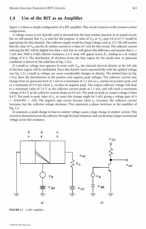
Figure 1.3 shows a simple configuration of a BJT amplifier. This circuit is known as the common emitterconfiguration.
A voltage source is not typically used to forward-bias the base–emitter junction in an actual circuit,but we will assume that VBB is used for this purpose. A value of VBB or VBE near 0.6 to 0.7 V would beappropriate for this situation. The collector supply would be a large voltage, such as 12 V. We will assumethat the value of VBB sets the dc emitter current to a value of 1 mA for this circuit. The collector currententering the BJT will be slightly less than 1 mA, but we will ignore this difference and assume that IC =1 mA also. With a 4-kW collector resistance, a 4-V drop will appear across RC , leading to a dc outputvoltage of 8 V. The distribution of electrons across the base region for the steady-state or quiescentconditions is shown by the solid line of Fig. 1.3(a).
If a small ac voltage now appears in series with VBB, the injected electron density at the left sideof the base region will be modulated. Since this density varies exponentially with the applied voltage(see Eq. 1.2), a small ac voltage can cause considerable changes in density. The dashed lines in Fig.1.3(a) show the distributions at the positive and negative peak voltages. The collector current maychange from its quiescent level of 1 mA to a maximum of 1.1 mA as ein reaches its positive peak, andto a minimum of 0.9 mA when ein reaches its negative peak. The output collector voltage will dropto a minimum value of 7.6 V as the collector current peaks at 1.1 mA, and will reach a maximumvoltage of 8.4 V as the collector current drops to 0.9 mA. The peak-to-peak ac output voltage is then0.8 V. The peak-to-peak value of ein to cause this change might be 5 mV, giving a voltage gain of A= –0.8/0.005 = –160. The negative sign occurs because when ein increases, the collector currentincreases, but the collector voltage decreases. This represents a phase inversion in the amplifier ofFig. 1.3.
In summary, a small change in base-to-emitter voltage causes a large change in emitter current. Thiscurrent is channeled across the collector, through the load resistance, and can develop a larger incrementalvoltage across this resistance.
FIGURE 1.3 A BJT amplifier.
© 2003 by CRC Press LLC

1-6 Analog Circuits and Devices
1.5 Representing the Major BJT Effects by an Electronic Model
The two major effects of the BJT in the active region are the diode characteristics of the base–emitterjunction and the collector current that is proportional to the emitter current. These effects can be modeledby the circuit of Fig. 1.4.
The simple diode equation represents the relationship between applied emitter-to-base voltage andemitter current. This equation can be written as
(1.6)
where q is the charge on an electron, k is Boltzmann’s constant, T is the absolute temperature of thediode, and I1 is a constant at a given temperature that depends on the doping and geometry of the emitter-base junction.
The collector current is generated by a dependent current source of value IC = aIE.
resistance, rd, is the dynamic resistance of the emitter-base diode and is given by:
(1.7)
where IE is the dc emitter current.
1.6 Other Physical Effects in the BJT
The preceding section pertains to the basic operation of the BJT in the dc and midband frequency range.Several other effects must be included to model the BJT with more accuracy. These effects will now bedescribed.
Ohmic Effects
The metal connections to the semiconductor regions exhibit some ohmic resistance. The emitter contactresistance and collector contact resistance is often in the ohm range and does not affect the BJT operationin most applications. The base region is very narrow and offers little area for a metal contact. Furthermore,because this region is narrow and only lightly doped compared to the emitter, the ohmic resistance ofthe base region itself is rather high. The total resistance between the contact and the intrinsic base regioncan be 100 to 200 W. This resistance can become significant in determining the behavior of the BJT,especially at higher frequencies.
FIGURE 1.4 Large-signal model of the BJT.
IE I1 eqVBE kT§
1–( )=
rdkTqIE
-------=
© 2003 by CRC Press LLC
A small-signal model based on the large-signal model of Fig. 1.4 is shown in Fig. 1.5. In this case, the

Bipolar Junction Transistor (BJT) Circuits 1-7
Base-Width Modulation (Early Effect)
The widths of the depletion regions are functions of the applied voltages. The collector voltage generallyexhibits the largest voltage change and, as this voltage changes, so also does the collector–base depletionregion width. As the depletion layer extends further into the base region, the slope of the electrondistribution in the base region becomes greater since the width of the base region is decreased. A slightlysteeper slope leads to slightly more collector current. As reverse-bias decreases, the base width becomesgreater and the current decreases. This effect is called base-width modulation and can be expressed interms of the Early voltage,4 VA, by the expression:
(1.8)
The Early voltage will be constant for a given device and is typically in the range of 60 to 100 V.
Reactive Effects
Changing the voltages across the depletion regions results in a corresponding change in charge. Thisleads to an effective capacitance since
(1.9)
This depletion region capacitance is a function of voltage applied to the junction and can be written as:4
(1.10)
where CJo is the junction capacitance at zero bias, f is the built-in junction barrier voltage, Vapp is theapplied junction voltage, and m is a constant. For modern BJTs, m is near 0.33. The applied junctionvoltage has a positive sign for a forward-bias and a negative sign for a reverse-bias. The depletion regioncapacitance is often called the junction capacitance.
An increase in forward base–emitter voltage results in a higher density of electrons injected into thebase region. The charge distribution in the base region changes with this voltage change, and this leadsto a capacitance called the diffusion capacitance. This capacitance is a function of the emitter current andcan be written as:
FIGURE 1.5 A small-signal model of the BJT.
IC bIB 1VCE
VA
--------+Ë ¯Ê ˆ=
C dQdV-------=
CdrCJo
f Vapp–( )m--------------------------=
© 2003 by CRC Press LLC

1-8 Analog Circuits and Devices
(1.11)
where k2 is a constant for a given device.
1.7 More Accurate BJT Models
Figure 1.6 shows a large-signal BJT model used in some versions of the popular simulation programknown as SPICE.5 The equations for the parameters are listed in other texts5 and will not be given here.
5
tance, Cp, accounts for the diffusion capacitance and the emitter–base junction capacitance. The collec-tor–base junction capacitance is designated Cm. The resistance, rp, is equal to (b + 1)rd. The transductance,gm, is given by:
(1.12)
The impedance, ro, is related to the Early voltage by:
(1.13)
RB, RE, and RC are the base, emitter, and collector resistances, respectively. For hand analysis, the ohmicresistances RE and RC are neglected along with CCS, the collector-to-substrate capacitance.
1.8 Heterojunction Bipolar Junction Transistors
In an npn device, all electrons injected from emitter to base are collected by the collector, except for asmall number that recombine in the base region. The holes injected from base to emitter contribute to
FIGURE 1.6 A more accurate large-signal model of the BJT.
CD k2IE=
gmard
----=
roVA
IC
------=
© 2003 by CRC Press LLC
Figure 1.7 shows a small-signal SPICE model often called the hybrid-p equivalent circuit. The capaci-

Bipolar Junction Transistor (BJT) Circuits 1-9
emitter junction current, but do not contribute to collector current. This hole component of the emittercurrent must be minimized to achieve a near-unity current gain from emitter to collector. As a approachesunity, the current gain from base to collector, b, becomes larger.
In order to produce high-b BJTs, the emitter region must be doped much more heavily than the baseregion, as explained earlier. While this approach allows the value of b to reach several hundred, it alsoleads to some effects that limit the frequency of operation of the BJT. The lightly doped base regioncauses higher values of base resistance, as well as emitter–base junction capacitance. Both of these effectsare minimized in the heterojunction BJT (or HBJT). This device uses a different material for the baseregion than that used for the emitter and collector regions. One popular choice of materials is siliconfor the emitter and collector regions, and a silicon/germanium material for the base region.6 The differencein energy gap between the silicon emitter material and the silicon/germanium base material results inan asymmetric barrier to current flow across the junction. The barrier for electron injection from emitterto base is smaller than the barrier for hole injection from base to emitter. The base can then be dopedmore heavily than a conventional BJT to achieve lower base resistance, but the hole flow across thejunction remains negligible due to the higher barrier voltage. The emitter of the HBJT can be dopedmore lightly to lower the junction capacitance. Large values of b are still possible in the HBJT whileminimizing frequency limitations. Current gain-bandwidth figures exceeding 60 GHz have been achievedwith present industrial HBJTs.
From the standpoint of analysis, the SPICE models for the HBJT are structurally identical to those ofthe BJT. The difference is in the parameter values.
1.9 Integrated Circuit Biasing Using Current Mirrors
Differential stages are very important in integrated circuit amplifier design. These stages require a constantdc current for proper bias. A simple bias scheme for differential BJT stages will now be discussed.
current bias for differential stages.The concept of the current mirror was developed specifically for analog integrated circuit biasing and
is a good example of a circuit that takes advantage of the excellent matching characteristics that arepossible in integrated circuits. In the circuit of Fig. 1.8, the current I2 is intended to be equal to or “mirror”the value of I1. Current mirrors can be designed to serve as sinks or sources.
[
FIGURE 1.7 The hybrid-p small-signal model for the BJT.
© 2003 by CRC Press LLC
The diode-biased current sink or current mirror of Fig. 1.8 is a popular method of creating a constant-

1-10 Analog Circuits and Devices
The general function of the current mirror is to reproduce or mirror the input or reference currentto the output, while allowing the output voltage to assume any value within some specified range. Thecurrent mirror can also be designed to generate an output current that equals the input current multipliedby a scale factor K. The output current can be expressed as a function of input current as:
(1.14)
where K can be equal to, less than, or greater than unity. This constant can be established accurately byrelative device sizes and will not vary with temperature.
the input current. Several amplifier stages can be biased with this multiple output current mirror.
Current Source Operating Voltage Range
Figure 1.10 shows an ideal or theoretical current sink in (a) and a practical sink in (b). The voltage atnode A in the theoretical sink can be tied to any potential above or below ground without affecting thevalue of I. On the other hand, the practical circuit of Fig. 1.10(b) requires that the transistor remain inthe active region to provide a current of:
(1.15)
This requires that the collector voltage exceed the voltage VB at all times. The upper limit on this voltageis determined by the breakdown voltage of the transistor. The output voltage must then satisfy:
(1.16)
where BVCE is the breakdown voltage from collector to emitter of the transistor. This voltage range overwhich the current source operates is called the output voltage compliance range or the output compliance.
FIGURE 1.8 Current mirror bias stage.
IO KIIN=
I aVB VBE–R
--------------------=
VB VC VB BVCE+( )< <
© 2003 by CRC Press LLC
Figure 1.9 shows a multiple output current source where all of the output currents are referenced to
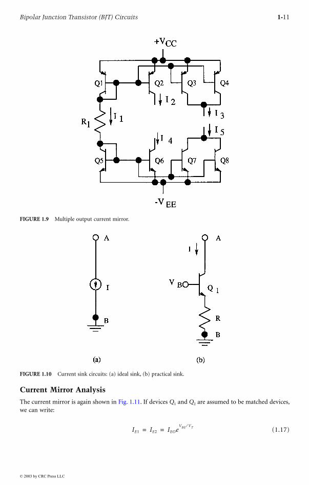
Bipolar Junction Transistor (BJT) Circuits 1-11
Current Mirror Analysis
The current mirror is again shown in Fig. 1.11. If devices Q1 and Q2 are assumed to be matched devices,we can write:
(1.17)
FIGURE 1.9 Multiple output current mirror.
FIGURE 1.10 Current sink circuits: (a) ideal sink, (b) practical sink.
IE1 IE2 IEOeVBE VT§
= =
© 2003 by CRC Press LLC

1-12 Analog Circuits and Devices
where VT = kT/q, IEO = AJEO, A is the emitter area of the two devices, and JEO is the current density ofthe emitters. The base currents for each device will also be identical and can be expressed as:
(1.18)
Device Q1 operates in the active region, but near saturation by virtue of the collector–base connection.This configuration is called a diode-connected transistor. Since the collector-to-emitter voltage is verysmall, the collector current for device Q1 is given by Eq. 1.8, assuming VCE = 0. This gives:
(1.19)
The device Q2 does not have the constraint that VCE ª 0 as device Q1 has. The collector voltage for Q2
will be determined by the external circuit that connects to this collector. Thus, the collector current forthis device is:
(1.20)
where VA is the Early voltage. In effect, the output stage has an output impedance given by Eq. 1.13. Thecurrent mirror more closely approximates a current source as the output impedance becomes larger.
If we limit the voltage VC2 to small values relative to the Early voltage, IC2 is approximately equal toIC1. For integrated circuit designs, the voltage required at the output of the current mirror is generallysmall, making this approximation valid.
The input current to the mirror is larger than the collector current and is:
(1.21)
Since IOUT = IC2 = IC1 = bIB, we can write Eq. 1.21 as:
(1.22)
FIGURE 1.11 Circuit for current mirror analysis.
IB1 IB2IEO
b 1+------------e
VBE VT§= =
IC1 bIB1b
b 1+------------IEOe
VBE VT§ª=
IC2 bIB2 1VC2
VA
--------+Ë ¯Ê ˆ=
IIN IC1 2IB+=
IIN bIB 2IB+ b 2+( )IB= =
© 2003 by CRC Press LLC

Bipolar Junction Transistor (BJT) Circuits 1-13
Relating IIN to IOUT results in:
(1.23)
For typical values of b, these two currents are essentially equal. Thus, a desired bias current, IOUT , isgenerated by creating the desired value of IIN. The current IIN is normally established by connecting aresistance R1 to a voltage source VCC to set IIN to:
(1.24)
Control of collector/bias current for Q2 is then accomplished by choosing proper values of VCC and R1.Figure 1.12 shows a multiple-output current mirror.It can be shown that the output current for each identical device in Fig. 1.12 is:
(1.25)
where N is the number of output devices.The current sinks can be turned into current sources by using pnp transistors and a power supply of
opposite polarity. The output devices can also be scaled in area to make IOUT larger or smaller than IIN.
Current Mirror with Reduced Error
The difference between output current in a multiple-output current mirror and the input current canbecome quite large if N is large. One simple method of avoiding this problem is to use an emitter follower
The emitter follower, Q0, has a current gain from base to collector of b + 1, reducing the differencebetween IO and IIN to:
(1.26)
FIGURE 1.12 Multiple-output current mirror.
IOUTb
b 2+------------IIN
IIN
1 2 b§+-------------------= =
IINVCC VBE–
R1
-----------------------=
IOIIN
1 N 1+b
-------------+-----------------------=
IIN IO– N 1+b 1+-------------IB=
© 2003 by CRC Press LLC
to drive the bases of all devices in the mirror, as shown in Fig. 1.13.
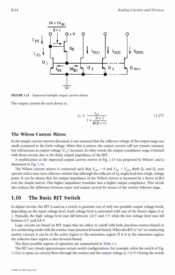
1-14 Analog Circuits and Devices
The output current for each device is:
(1.27)
The Wilson Current Mirror
In the simple current mirrors discussed, it was assumed that the collector voltage of the output stage wassmall compared to the Early voltage. When this is untrue, the output current will not remain constant,but will increase as output voltage (VCE) increases. In other words, the output compliance range is limitedwith these circuits due to the finite output impedance of the BJT.
A modification of the improved output current mirror of Fig. 1.13 was proposed by Wilson7 and is
The Wilson current mirror is connected such that VCB2 = 0 and VBE1 = VBE0. Both Q1 and Q2 nowoperate with a near-zero collector–emitter bias although the collector of Q0 might feed into a high-voltagepoint. It can be shown that the output impedance of the Wilson mirror is increased by a factor of b/2over the simple mirror. This higher impedance translates into a higher output compliance. This circuitalso reduces the difference between input and output current by means of the emitter follower stage.
1.10 The Basic BJT Switch
In digital circuits, the BJT is used as a switch to generate one of only two possible output voltage levels,depending on the input voltage level. Each voltage level is associated with one of the binary digits, 0 or1. Typically, the high voltage level may fall between 2.8 V and 5 V while the low voltage level may fallbetween 0 V and 0.8 V.
Logic circuits are based on BJT stages that are either in cutoff with both junctions reverse-biased orin a conducting mode with the emitter–base junction forward-biased. When the BJT is “on” or conductingemitter current, it can be in the active region or the saturation region. If it is in the saturation region,the collector–base region is also forward-biased.
FIGURE 1.13 Improved multiple output current mirror.
IOIIN
1 N 1+b b 1+( )---------------------+
------------------------------=
© 2003 by CRC Press LLC
The three possible regions of operation are summarized in Table 1.1.
illustrated in Fig. 1.14.
The BJT very closely approximates certain switch configurations. For example, when the switch of Fig.1.15(a) is open, no current flows through the resistor and the output voltage is +12 V. Closing the switch

Bipolar Junction Transistor (BJT) Circuits 1-15
causes the output voltage to drop to zero volts and a current of 12/R flows through the resistance. When
The output voltage is +12 V, just as in the case of the open switch. If a large enough current is now driveninto the base to saturate the BJT, the output voltage becomes very small, ranging from 20 mV to 500mV, depending on the BJT used. The saturated state corresponds closely to the closed switch. Duringthe time that the BJT switches from cutoff to saturation, the active region equivalent circuit applies. Forhigh-speed switching of this circuit, appropriate reactive effects must be considered. For low-speedswitching, these reactive effects can be neglected.
Saturation occurs in the basic switching circuit of Fig. 1.15(b) when the entire power supply voltagedrops across the load resistance. No voltage, or perhaps a few tenths of volts, then appears from collectorto emitter. This occurs when the base current exceeds the value
(1.28)
When a transistor switch is driven into saturation, the collector–base junction becomes forward-
The forward-bias of the collector–base junction leads to a non zero concentration of electrons inthe base that is unnecessary to support the gradient of carriers across this region. When the inputsignal to the base switches to a lower level to either turn the device off or decrease the currentflow, the excess charge must be removed from the base region before the current can begin todecrease.
FIGURE 1.14 Wilson current mirror.
TABLE 1.1 Regions of Operation
Region Cutoff Active Saturation
C–B bias Reverse Reverse ForwardE–B bias Reverse Forward Forward
IB sat( )VCC VCE sat( )–
bRL
-------------------------------=
© 2003 by CRC Press LLC
the base voltage of the BJT of Fig. 1.15(b) is negative, the device is cut off and no collector current flows.
biased. This situation results in the electron distribution across the base region shown in Fig. 1.16.

1-16 Analog Circuits and Devices
1.11 High-Speed BJT Switching
There are three major effects that extend switching times in a BJT:
1. The depletion-region or junction capacitances are responsible for delay time when the BJT is inthe cutoff region.
2. The diffusion capacitance and the Miller-effect capacitance are responsible for the rise and falltimes of the BJT as it switches through the active region.
3. The storage time constant accounts for the time taken to remove the excess charge from the baseregion before the BJT can switch from the saturation region to the active region.
FIGURE 1.15 The BJT as a switch: (a) open switch, (b) closed switch.
FIGURE 1.16 Electron distribution in the base region of a saturated BJT.
© 2003 by CRC Press LLC

Bipolar Junction Transistor (BJT) Circuits 1-17
There are other second-order effects that are generally negligible compared to the previously listedtime lags.
Since the transistor is generally operating as a large-signal device, the parameters such as junctioncapacitance or diffusion capacitance will vary as the BJT switches. One approach to the evaluation oftime constants is to calculate an average value of capacitance over the voltage swing that takes place.Notonly is this method used in hand calculations, but most computer simulation programs use averagevalues to speed calculations.
Overall Transient Response
Before discussing the individual BJT switching times, it is helpful to consider the response of a common-emitter switch to a rectangular waveform. Figure 1.17 shows a typical circuit using an npn transistor.
circuits, the BJT must switch from its “off” state to saturation and later return to the “off” state. In thiscase, the delay time, rise time, saturation storage time, and fall time must be considered in that order tofind the overall switching time.
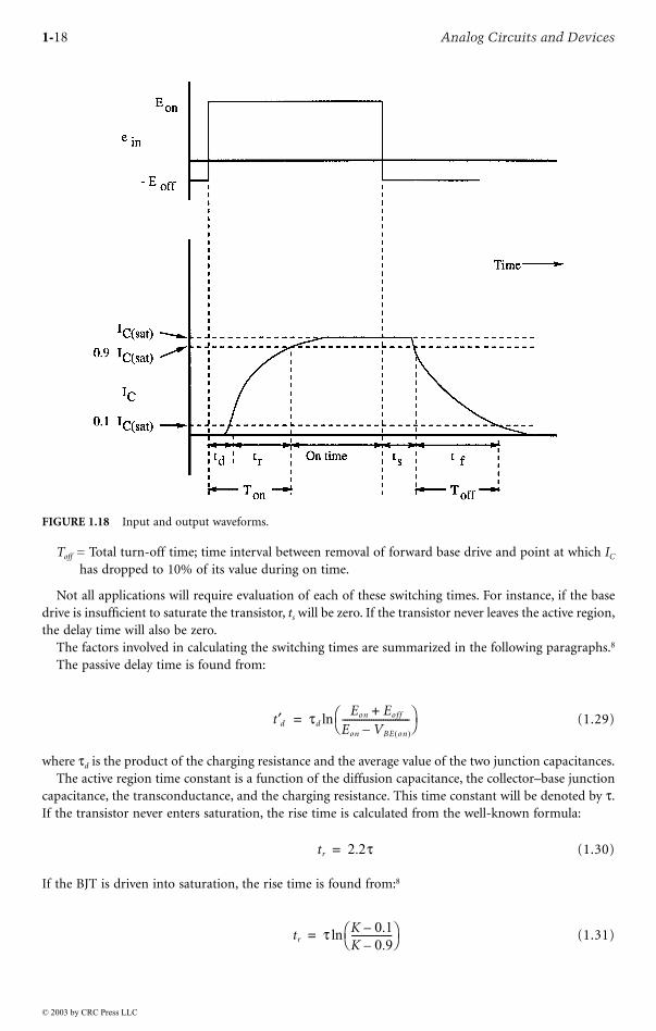
The total waveform is made up of five sections: delay time, rise time, on time, storage time, and falltime. The following list summarizes these points and serves as a guide for future reference:
td¢ = Passive delay time; time interval between application of forward base drive and start of collector-current response.
td = Total delay time; time interval between application of forward base drive and the point at whichIC has reached 10% of the final value.
tr = Rise time; 10- to 90-% rise time of IC waveform.ts¢ = Saturation storage time; time interval between removal of forward base drive and start of IC decrease.ts = Total storage time; time interval between removal of forward base drive and point at which IC =
0.9IC(sat).tf = Fall time; 90- to 10-% fall time of IC waveformTon = Total turn-on time; time interval between application of base drive and point at which IC has
reached 90% of its final value.
FIGURE 1.17 A simple switching circuit.
© 2003 by CRC Press LLC
A rectangular input pulse and the corresponding output are shown in Fig. 1.18. In many switching
1-18 Analog Circuits and Devices
Toff = Total turn-off time; time interval between removal of forward base drive and point at which IC
has dropped to 10% of its value during on time.
Not all applications will require evaluation of each of these switching times. For instance, if the basedrive is insufficient to saturate the transistor, ts will be zero. If the transistor never leaves the active region,the delay time will also be zero.
The factors involved in calculating the switching times are summarized in the following paragraphs.8
The passive delay time is found from:
(1.29)
where td is the product of the charging resistance and the average value of the two junction capacitances.The active region time constant is a function of the diffusion capacitance, the collector–base junction
capacitance, the transconductance, and the charging resistance. This time constant will be denoted by t.If the transistor never enters saturation, the rise time is calculated from the well-known formula:
(1.30)
If the BJT is driven into saturation, the rise time is found from:8
(1.31)
FIGURE 1.18 Input and output waveforms.
t¢d tdEon Eoff+
Eon VBE on( )–----------------------------Ë ¯
Ê ˆln=
tr 2.2t=
tr t K 0.1–K 0.9–-----------------Ë ¯
Ê ˆln=
© 2003 by CRC Press LLC

Bipolar Junction Transistor (BJT) Circuits 1-19
where K is the overdrive factor or the ratio of forward base current drive to the value needed for saturation.The rise time for the case where K is large can be much smaller than the rise time for the nonsaturatingcase (K < 1). Unfortunately, the saturation storage time increases for large values of K.
The saturation storage time is given by:
(1.32)
where ts is the storage time constant, IB1 is the forward base current before switching, and IB2 is thecurrent after switching and must be less than IB(sat). The saturation storage time can slow the overallswitching time significantly. The higher speed logic gates utilize circuits that avoid the saturation regionfor the BJTs that make up the gate.
1.12 Simple Logic Gates
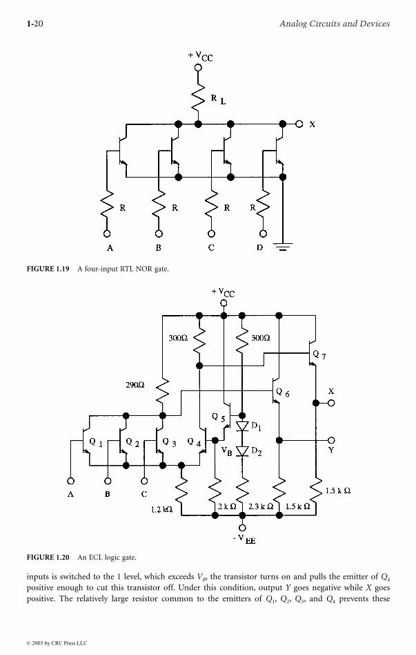
Although the resistor-transistor-logic (RTL) family has not been used since the late 1960s, it demonstrates
If all four inputs are at the lower voltage level (e.g., 0 V), there is no conducting path from output toground. No voltage will drop across RL, and the output voltage will equal VCC. If any or all of the inputsmove to the higher voltage level (e.g., 4 V), any BJT with base connected to the higher voltage level willsaturate, pulling the output voltage down to a few tenths of a volt. If positive logic is used, with the highvoltage level corresponding to binary “1” and the low voltage level to binary “0,” the gate performs theNOR function. Other logic functions can easily be constructed in the RTL family.
Over the years, the performance of logic gates has been improved by different basic configurations.RTL logic was improved by diode-transistor-logic (DTL). Then, transistor-transistor-logic (TTL) becamevery prominent. This family is still popular in the small-scale integration (SSI) and medium-scaleintegration (MSI) areas, but CMOS circuits have essentially replaced TTL in large-scale integration (LSI)and very-large-scale integration (VLSI) applications.
One popular family that is still prominent in very high-speed computer work is the emitter-coupledlogic (ECL) family. While CMOS packs many more circuits into a given area than ECL, the frequencyperformance of ECL leads to its popularity in supercomputer applications.
1.13 Emitter-Coupled Logic
Emitter-coupled logic (ECL) was developed in the mid-1960s and remains the fastest silicon logic circuitavailable. Present ECL families offer propagation delays in the range of 0.2 ns.9 The two major disadvan-tages of ECL are: (1) resistors which require a great deal of IC chip area, must be used in each gate, and.(2) the power dissipation of an ECL gate is rather high. These two shortcomings limit the usage of ECLin VLSI systems. Instead, this family has been used for years in larger supercomputers that can affordspace and power to achieve higher speeds.
The high speeds obtained with ECL are primarily based on two factors. No device in an ECL gate isever driven into the saturation region and, thus, saturation storage time is never involved as devicesswitch from one state to another. The second factor is that required voltage swings are not large. Voltageexcursions necessary to change an input from the low logic level to the high logic level are minimal.Although noise margins are lower than other logic families, switching times are reduced in this way.
while Y is the NOR output.Often, the positive supply voltage is taken as 0 V and VEE as –5 V due to noise considerations. The
diodes and emitter follower Q5 establish a temperature-compensated base reference for Q4. When inputsA, B, and C are less than the voltage VB, Q4 conducts while Q1, Q2, and Q3 are cut off. If any one of the
t¢s tsIB1 IB2–
IB sat( ) IB2–------------------------Ë ¯
Ê ˆln=
© 2003 by CRC Press LLC
the concept of a simple logic gate. Figure 1.19 shows a four-input RTL NOR gate.
Figure 1.20 shows an older ECL gate with two separate outputs. For positive logic, X is the OR output
1-20 Analog Circuits and Devices
inputs is switched to the 1 level, which exceeds VB, the transistor turns on and pulls the emitter of Q4
positive enough to cut this transistor off. Under this condition, output Y goes negative while X goespositive. The relatively large resistor common to the emitters of Q1, Q2, Q3, and Q4 prevents these
FIGURE 1.19 A four-input RTL NOR gate.
FIGURE 1.20 An ECL logic gate.
© 2003 by CRC Press LLC

Bipolar Junction Transistor (BJT) Circuits 1-21
transistors from saturating. In fact, with nominal logic levels of –1.9 V and –1.1 V, the current throughthe emitter resistance is approximately equal before and after switching takes place. Thus, only the currentpath changes as the circuit switches. This type of operation is sometimes called current mode switching.Although the output stages are emitter followers, they conduct reasonable currents for both logic leveloutputs and, therefore, minimize the asymmetrical output impedance problem.
In an actual ECL gate, the emitter follower load resistors are not fabricated on the chip. The newerversion of the gate replaces the emitter resistance of the differential stage with a current source, andreplaces the bias voltage circuit with a regulated voltage circuit.
A Closer Look at the Differential Stage2
are biased by a current source, IT , called the tail current. The two input signals e1 and e2 make up adifferential input signal defined as:
(1.33)
This differential voltage can be expressed as the difference between the base–emitter junction voltages as:
(1.34)
The collector currents can be written in terms of the base–emitter voltages as:
(1.35)
(1.36)
where matched devices are assumed.A differential output current can be defined as the difference of the collector currents, or
(1.37)
Since the tail current is IT = IC1 + IC2, taking the ratio of Id to IT gives:
(1.38)
Since VBE1 = ed + VBE2, we can substitute this value for VBE1 into Eq. 1.35 to write:
(1.39)
Substituting Eqs. 1.36 and 1.39 into Eq. 1.38 results in:
(1.40)
or
ed e1 e2–=
ed VBE1 VBE2–=
IC1 aIEOeVBE1 VT§
IEOeVBE1 VT§
ª=
IC2 aIEOeVBE2 VT§
IEOeVBE2 VT§
ª=
Id IC1 IC2–=
Id
IT
----IC1 IC2–IC1 IC2+-------------------=
IC1 IEOeed VBE2+( ) VT§
IEOeed VT§
eVBE2 VT§
= =
Id
IT
---- eed VT§
1–
eed VT§
1+---------------------
ed
2VT
---------tanh= =
© 2003 by CRC Press LLC
Figure 1.21 shows a simple differential stage similar to the input stage of an ECL gate. Both transistors

1-22 Analog Circuits and Devices
(1.41)
This differential current is graphed in Fig. 1.22.When ed is zero, the differential current is also zero, implying equal values of collector currents in the
two devices. As ed increases, so also does Id until ed exceeds 4VT , at which time Id has reached a constantvalue of IT . From the definition of differential current, this means that IC1 equals IT while IC2 is zero. Asthe differential input voltage goes negative, the differential current approaches –IT as the voltage reaches–4VT . In this case, IC2 = IT while IC1 goes to zero.
The implication here is that the differential stage can move from a balanced condition with IC1 = IC2
to a condition of one device fully off and the other fully on with an input voltage change of around 100mV or 4VT . This demonstrates that a total voltage change of about 200 mV at the input can cause anECL gate to change states. This small voltage change contributes to smaller switching times for ECL logic.
FIGURE 1.21 A simple differential stage similar to an ECL input stage.
FIGURE 1.22 Differential output current as a function of differential input voltage.
Id IT
ed
2VT
---------tanh=
© 2003 by CRC Press LLC

Bipolar Junction Transistor (BJT) Circuits 1-23
The ability of a differential pair to convert a small change in differential base voltage to a large changein collector voltage also makes it a useful building block for analog amplifiers. In fact, a differential pairwith a pnp transistor current mirror load, as illustrated in Fig. 1.23, is widely used as an input stage forintegrated circuit op-amps.
References
1. Brittain, J. E. (Ed.), Turning Points in American Electrical History, IEEE Press, New York, 1977, Sec.II-D.
2. Comer, D. T., Introduction to Mixed Signal VLSI, Array Publishing, New York, 1994, Ch. 7.3. Sedra, A. S. and Smith, K. C., Microelectronic Circuits, 4th ed., Oxford University Press, New York,
1998, Ch. 4.4. Gray, P. R. and Meyer, R. G., Analysis and Design of Analog Integrated Circuits, 3rd ed., John Wiley
& Sons, Inc., New York, 1993, Ch. 1.5. Vladimirescu, A., The Spice Book, John Wiley & Sons, Inc., New York, 1994, Ch. 3.6. Streetman, B. G., Solid State Electronic Devices, 4th ed., Prentice-Hall, Englewood Cliffs, NJ, 1995,
Ch. 7.7. Wilson, G. R., “A monolithic junction FET - NPN operational amplifier,” IEEE J. Solid-State Circuits,
Vol. SC-3, pp. 341-348, Dec. 1968.8. Comer, D. J., Modern Electronic Circuit Design, Addison-Wesley, Reading, MA, 1977, Ch. 8.9. Motorola Technical Staff, High Performance ECL Data, Motorola, Inc., Phoenix, AZ, 1993, Ch. 3.
FIGURE 1.23 Differential input stage with current mirror load.
© 2003 by CRC Press LLC