Bipolar Junction Transistor (BJT) - inc.kmutt.ac.thinc.kmutt.ac.th/course/inc223/lecture5 Bipolar...
45
1 Bipolar Junction Transistor (BJT)
-
Upload
hoangxuyen -
Category
Documents
-
view
267 -
download
1
Transcript of Bipolar Junction Transistor (BJT) - inc.kmutt.ac.thinc.kmutt.ac.th/course/inc223/lecture5 Bipolar...

1
Bipolar Junction Transistor(BJT)
2
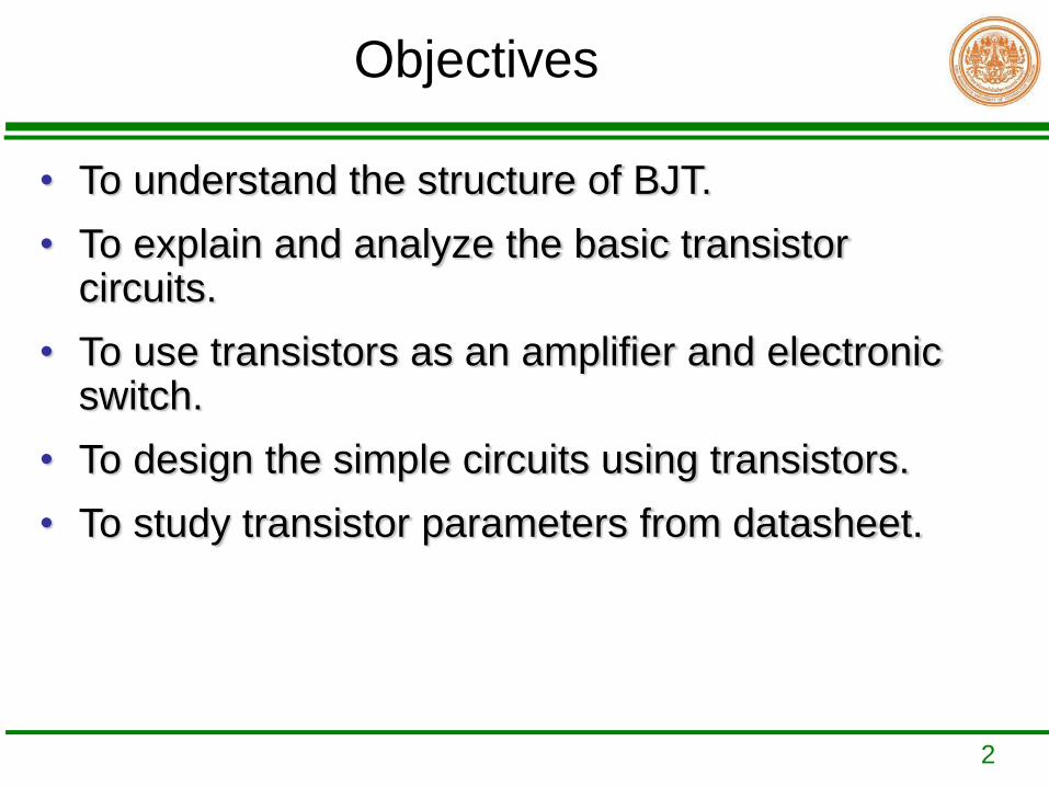
• To understand the structure of BJT.
• To explain and analyze the basic transistor circuits.
• To use transistors as an amplifier and electronic switch.
• To design the simple circuits using transistors.
• To study transistor parameters from datasheet.
Objectives

3
What is Transistor?
Transistor in 1947
• Invented in 1947 by John Bardeen, Walter Brattain and William Shockley
• Hugh revolution in field of electronics
• First solid-state device able to amplify electric signal
• Universally used is Bipolar Junction Transistor(BJT)

4
Transistor Structure
With diodes there is one p-n junction. With bipolar junction
transistors (BJT), there are three layers and two p-n
junctions..

5
Conducting Current Direction

6
Basic Functions
• Signal Amplifier
• Electronic Switch
2 Types

7
Basic Operation
Look at this one circuit as two separate circuits, the base-emitter(left
side) circuit and the collector-emitter(right side) circuit. Note that the
emitter leg serves as a conductor for both circuits. The amount of current
flow in the base-emitter circuit controls the amount of current that flows in
the collector circuit. Small changes in base-emitter current yields a large
change in collector-current.
8
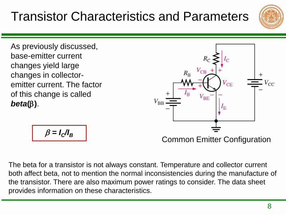
Transistor Characteristics and Parameters
As previously discussed,
base-emitter current
changes yield large
changes in collector-
emitter current. The factor
of this change is called
beta().
= IC/IBCommon Emitter Configuration
The beta for a transistor is not always constant. Temperature and collector current
both affect beta, not to mention the normal inconsistencies during the manufacture of
the transistor. There are also maximum power ratings to consider. The data sheet
provides information on these characteristics.

9
For proper operation, the base-emitter junction is forward-biased by VBB
and conducts just like a diode.
The collector-base junction is reverse biased by VCC and blocks current
flow through it’s junction just like a diode.
Remember that
current flow through
the base-emitter
junction will help
establish the path for
current flow from the
collector to emitter.
B-E Forward biased
B-C Reverse biased

10
There are three key dc voltages and three key dc currents to be considered.
Note that these measurements are important for troubleshooting.
IB: dc base current
IE: dc emitter current
IC: dc collector current
VBE: dc voltage across
base-emitter junction
VCB: dc voltage across
collector-base junction
VCE: dc voltage from
collector to emitter

11
Analysis of this transistor circuit to predict the dc voltages and currents requires
use of Ohm’s law, Kirchhoff’s voltage law and the beta for the transistor.
Application of these laws begins with the base circuit to determine the amount of
base current. Using Kirchhoff’s voltage law, subtract the .7 VBE and the remaining
voltage is dropped across RB. Determining the current for the base with this
information is a matter of applying of Ohm’s law. IB = VRB/RB
The collector current is determined by
multiplying the base current by beta.
Note. VBE = 0.7 will be used in most analysis examples.
What we ultimately determine by use of Kirchhoff’s voltage law for series circuits is
that in the base circuit VBB is distributed across the base-emitter junction and RB in
the base circuit. In the collector circuit we determine that VCC is distributed
proportionally across RC and the transistor(VCE).

Collector characteristic curves give a graphical illustration of the relationship of collector current and VCE with
specified amounts of base current. With greater increases of VCC , VCE continues to increase until it reaches
breakdown, but the current remains about the same in the linear region from .7V to the breakdown voltage.

13
Transistor regions
Curve shown for one fixed base current (IB)
VCE increased, Ic increased until B
FlatIB
14
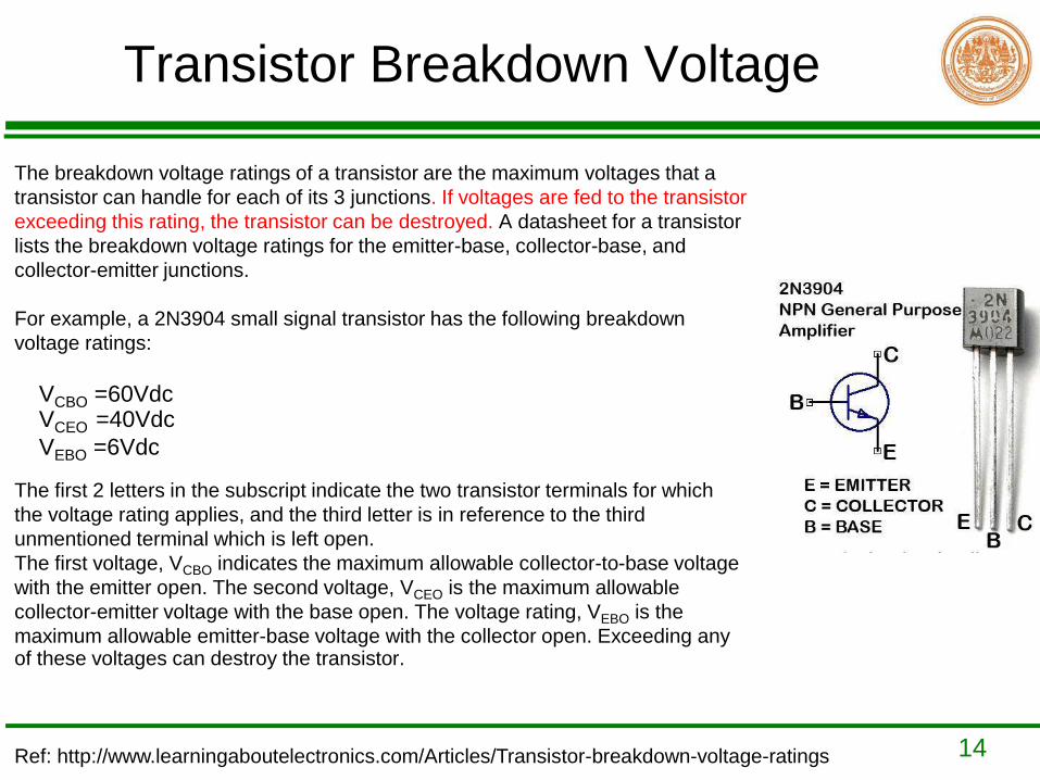
Transistor Breakdown Voltage
The breakdown voltage ratings of a transistor are the maximum voltages that a
transistor can handle for each of its 3 junctions. If voltages are fed to the transistor
exceeding this rating, the transistor can be destroyed. A datasheet for a transistor
lists the breakdown voltage ratings for the emitter-base, collector-base, and
collector-emitter junctions.
For example, a 2N3904 small signal transistor has the following breakdown
voltage ratings:
The first 2 letters in the subscript indicate the two transistor terminals for which
the voltage rating applies, and the third letter is in reference to the third
unmentioned terminal which is left open.
The first voltage, VCBO indicates the maximum allowable collector-to-base voltage
with the emitter open. The second voltage, VCEO is the maximum allowable
collector-emitter voltage with the base open. The voltage rating, VEBO is the
maximum allowable emitter-base voltage with the collector open. Exceeding any of these voltages can destroy the transistor.
VCBO =60VdcVCEO =40Vdc
VEBO =6Vdc
Ref: http://www.learningaboutelectronics.com/Articles/Transistor-breakdown-voltage-ratings

16
17
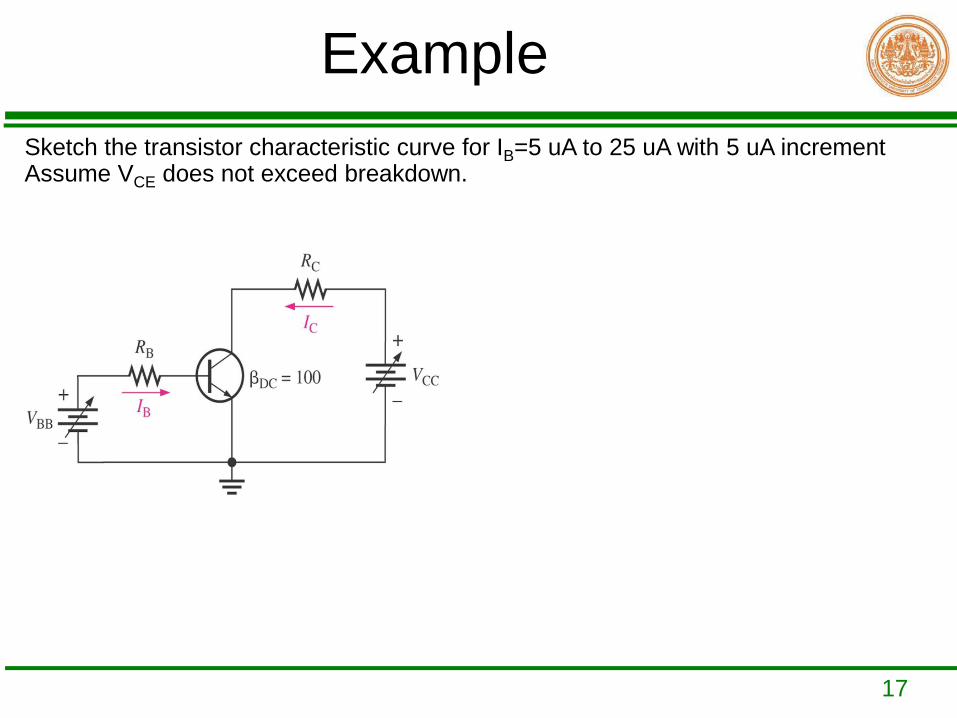
Example
Sketch the transistor characteristic curve for IB=5 uA to 25 uA with 5 uA incrementAssume VCE does not exceed breakdown.
18
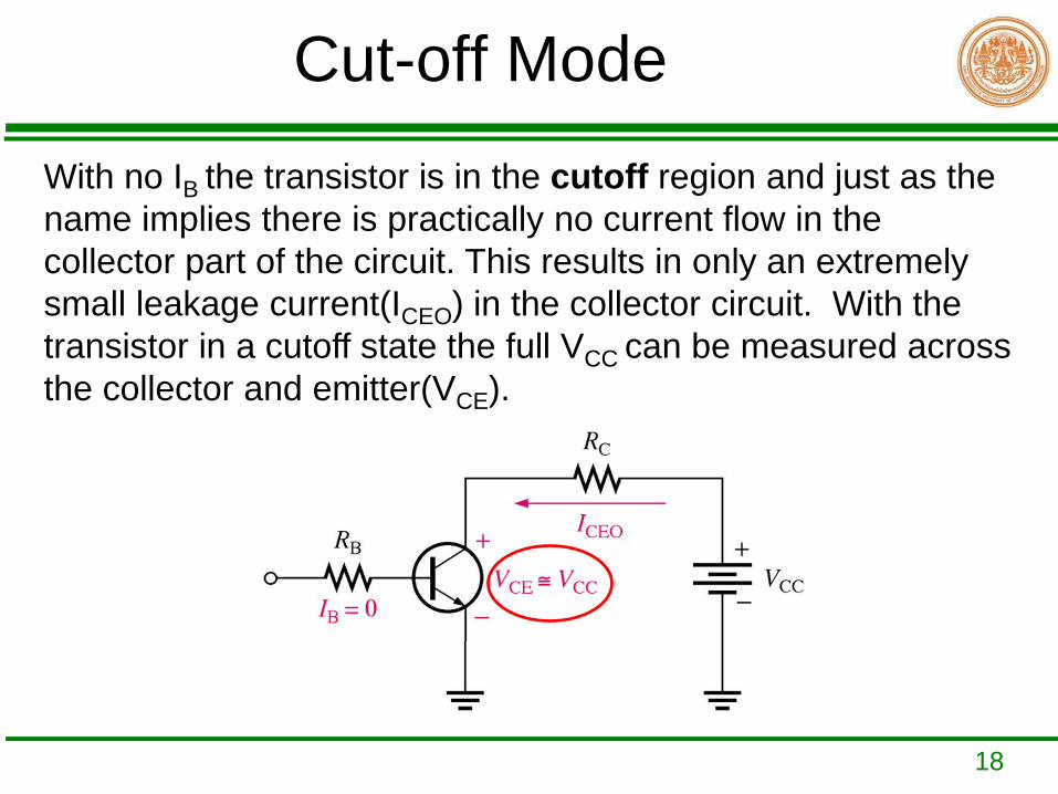
Cut-off Mode
With no IB the transistor is in the cutoff region and just as the
name implies there is practically no current flow in the
collector part of the circuit. This results in only an extremely
small leakage current(ICEO) in the collector circuit. With the
transistor in a cutoff state the full VCC can be measured across
the collector and emitter(VCE).

19
Saturation Mode
Current flow in the collector part of the circuit is, as stated previously,
determined by IB multiplied by . However, there is a limit to how much
current can flow in the collector circuit regardless of additional increases in IB. Once this maximum is reached, the transistor is said to be in saturation. Note that
saturation can be determined by application of Ohm’s law, IC(sat)=(VCC - VCE ) /RC .
For Ideal case, the measured voltage across the now “shorted” collector and
emitter(VCE) is 0V. The practical value is around 0.2V
Figure. Saturation: As IB increases due to increasing VBB, IC also increases and VCE decreases due to the increased voltage drop
across RC. When the transistor reaches saturation, IC can increase no further regardless of further increase in IB.
In saturation, an increase of base current
has no effect on collector circuit and the
relationship IC =.IB is no longer valid.

20
Example
• Determine whether or not the transistor is in saturation. Assume VCE(sat)=0.2V.
21
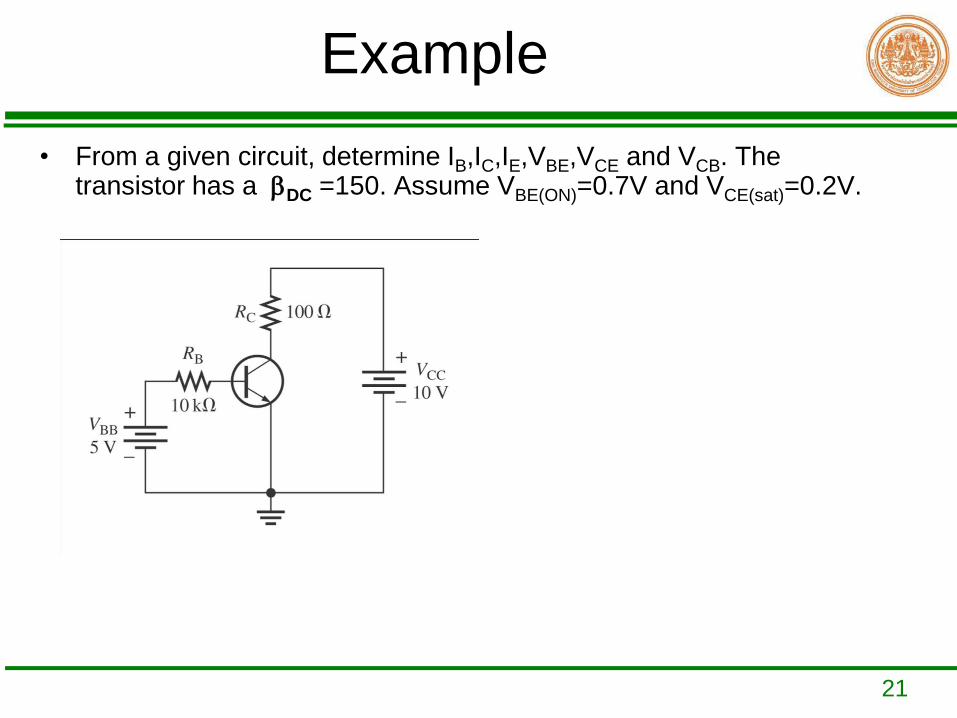
Example
• From a given circuit, determine IB,IC,IE,VBE,VCE and VCB. The transistor has a DC =150. Assume VBE(ON)=0.7V and VCE(sat)=0.2V.
22
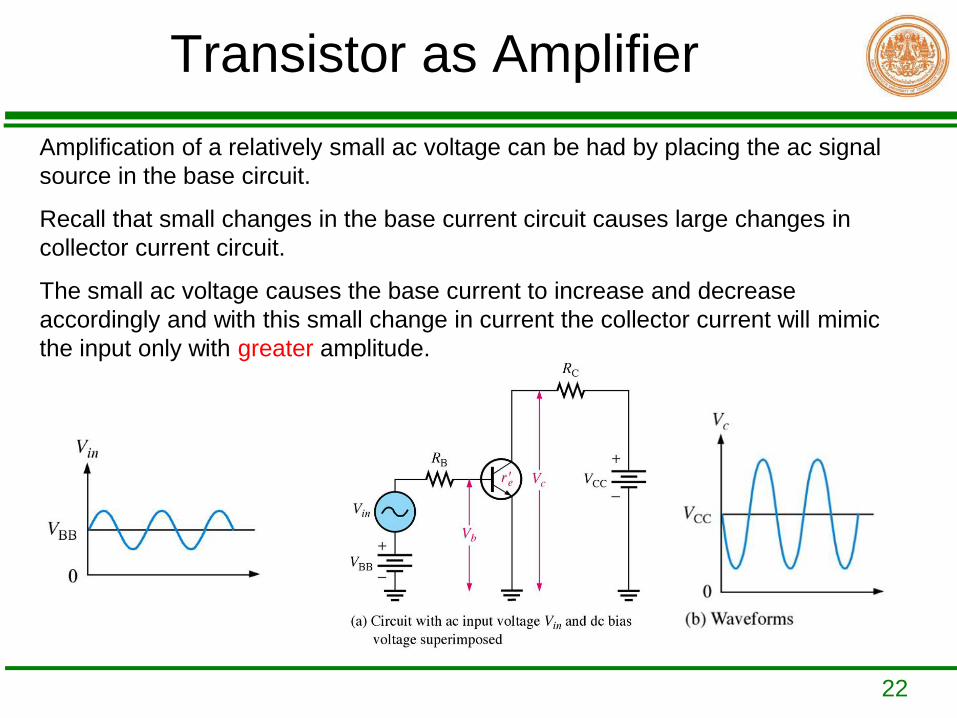
Transistor as Amplifier
Amplification of a relatively small ac voltage can be had by placing the ac signal
source in the base circuit.
Recall that small changes in the base current circuit causes large changes in
collector current circuit.
The small ac voltage causes the base current to increase and decrease
accordingly and with this small change in current the collector current will mimic
the input only with greater amplitude.
23
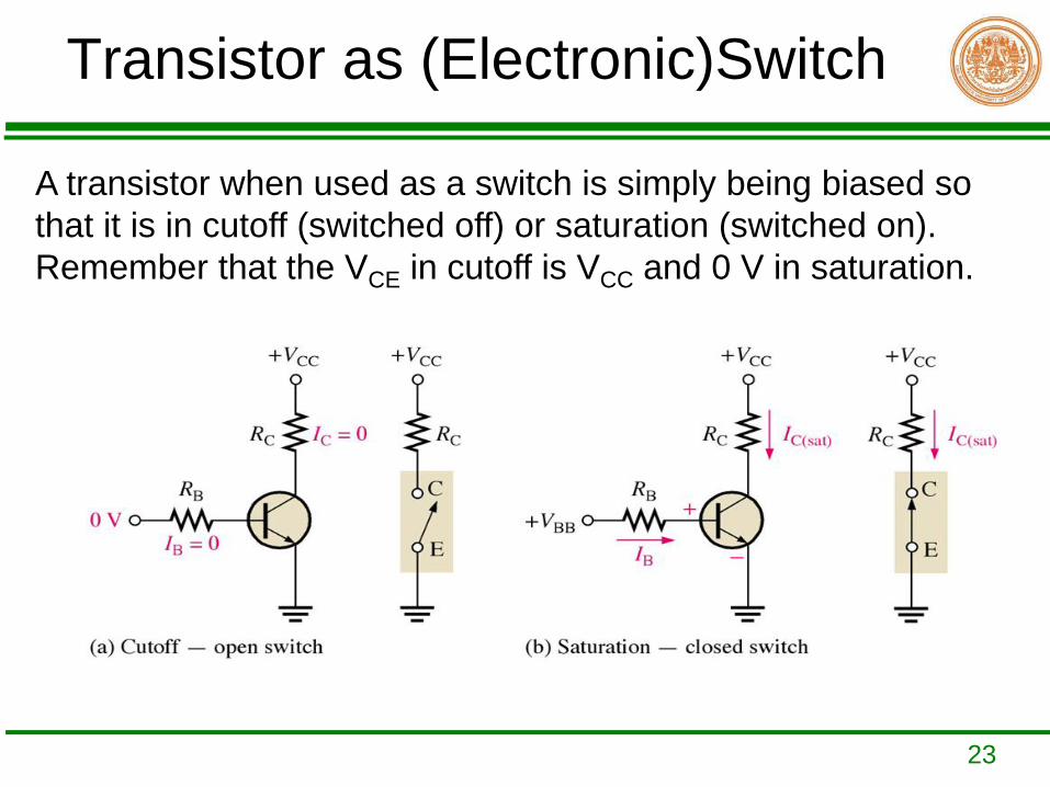
Transistor as (Electronic)Switch
A transistor when used as a switch is simply being biased so
that it is in cutoff (switched off) or saturation (switched on).
Remember that the VCE in cutoff is VCC and 0 V in saturation.
24
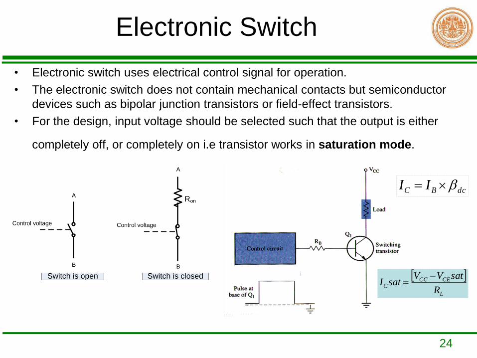
Electronic Switch
• Electronic switch uses electrical control signal for operation.
• The electronic switch does not contain mechanical contacts but semiconductor
devices such as bipolar junction transistors or field-effect transistors.
• For the design, input voltage should be selected such that the output is either
completely off, or completely on i.e transistor works in saturation mode.
dcBC II
L
CECCC
R
satVVsatI
Control voltage
A
B
Control voltage
A
B
Ron
Switch is open Switch is closed

25
Application (as electronic switch)
The LED in a given circuit requires 30mA to emit a sufficient light. Determine
the amplitude of square wave necessary to make sure the LED emit sufficient
Light. Use double the minimum value of base current as a safety margin to
ensure saturation. VCC=9V,VCE(SAT)=0.3V, RC=220Ω , RB=3.3kΩ, DC = 50,and VLED=1.6V.

26
Application (driving relay)
From a relay driving circuit below, assume relay coil resistance = 250 Ohms,VDC = 12 V, DC current gain of transistor = 100 and VCE(SAT) = 0.1 V.
Vin is 0-5 V. If this relay requires 40 mA for operation , calculate RB .
RB
+VDC
NC
C
NO
AC
AC
bulb
Vin
coil
Relay

27
Plastic cases for general-purpose/small-signal transistors.

28
Metal cases for general-purpose/small-signal transistors

29
Power Transistors


31
Example
Find beta or hFE or dc current gain
= ________

32
Example
Refer to the datasheet. Determine whether or not the transistor is saturatedin each circuit based on the maximum specific value of hFE .

34
Hint for hFE Selection
The datasheet shows that the hFE can not be
specified precisely by the manufacturer, because it
varies very much between transistors and with
electrical and thermal conditions. However, it is
possible to get an approximated value.
Students can start with the roughly calculation of Ic.
For example, if Ic =20mA, we can take an
intermediate value between the hFE for Ic=2mA (500) and the hFE for Ic =100mA (400), so
let's take hFE =450.

35
Example
• Determine IB,IC,IE and DC .

36
Example
• Find VCE,VBE,VCB in both circuits.
37
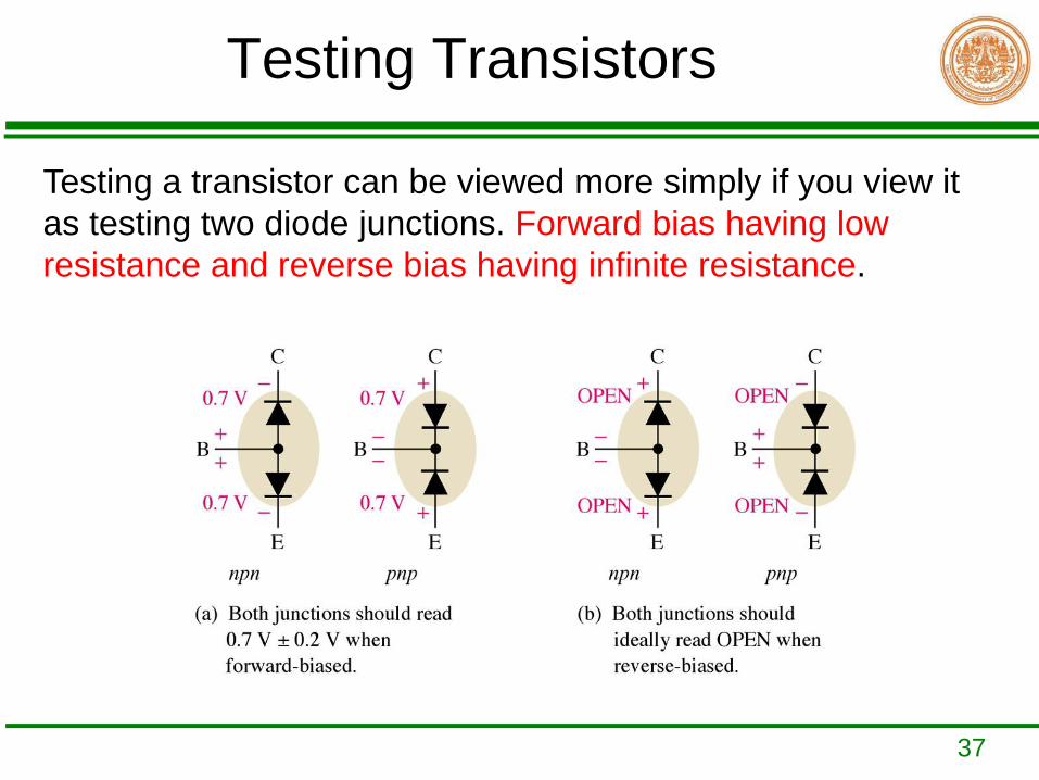
Testing Transistors
Testing a transistor can be viewed more simply if you view it
as testing two diode junctions. Forward bias having low
resistance and reverse bias having infinite resistance.

38
The diode test function of a multimeter is more reliable than
using an ohmmeter. Make sure to note whether it is an npn
or pnp and polarize the test leads accordingly.
In addition to the traditional DMMs there are also transistor testers. Some of these
have the ability to test other parameters of the transistor, such as leakage and gain.
Curve tracers give us even more detailed information about a transistors
characteristics.

39
Conclusions
The bipolar junction transistor (BJT) is constructed of three regions: base, collector, and emitter.
The BJT has two pn junctions, the base-emitter junction and the base-collector junction.
The two types of transistors are pnp and npn.
For the BJT to operate as an amplifier, the base-emitter junction is forward-biased and the collector-base
junction is reverse-biased.
Of the three currents IB is very small in comparison to IE and IC.
Beta is the current gain of a transistor. This the ratio of IC/IB.
A transistor can be operated as an electronics switch.
When the transistor is off it is in cutoff condition (no current).
When the transistor is on, it is in saturation condition (maximum current).
Beta can vary with temperature and also varies from transistor to transistor.

40
Supplement

41
Relays
• A relay is an electrically operated switch. Current flowing through the coil of
the relay creates a magnetic field which attracts a lever and changes the switch contacts. The coil current can be on or off so relays have two switch positions
and they are double throw (changeover) switches.
SPDT Relays
DPDT Relays
Symbol

42

43
Solid State Relays(SSRs)
• Solid state relay (SSR) is a solid state electronic component that provides a similar function to an electromechanical relay but does not have any moving components, increasing long-term reliability. have become commercially available.
• The types of SSR are photo-coupled SSR, transformer-coupled SSR, and hybrid SSR. A photo-coupled SSR is controlled by a low voltage signal which is isolated optically from the load. The control signal in a photo-coupled SSR typically energizes an LED which activates a photo-sensitive diode. The diode turns on switching devices i.e. a back-to-back thyristor, silicon controlled rectifier, or MOSFET transistor to power on the load.
• Control input can be AC,DC, 4-20 mA, etc
• Adv: fast, smaller,lifetime
Disadv: false triggering, expensive

44
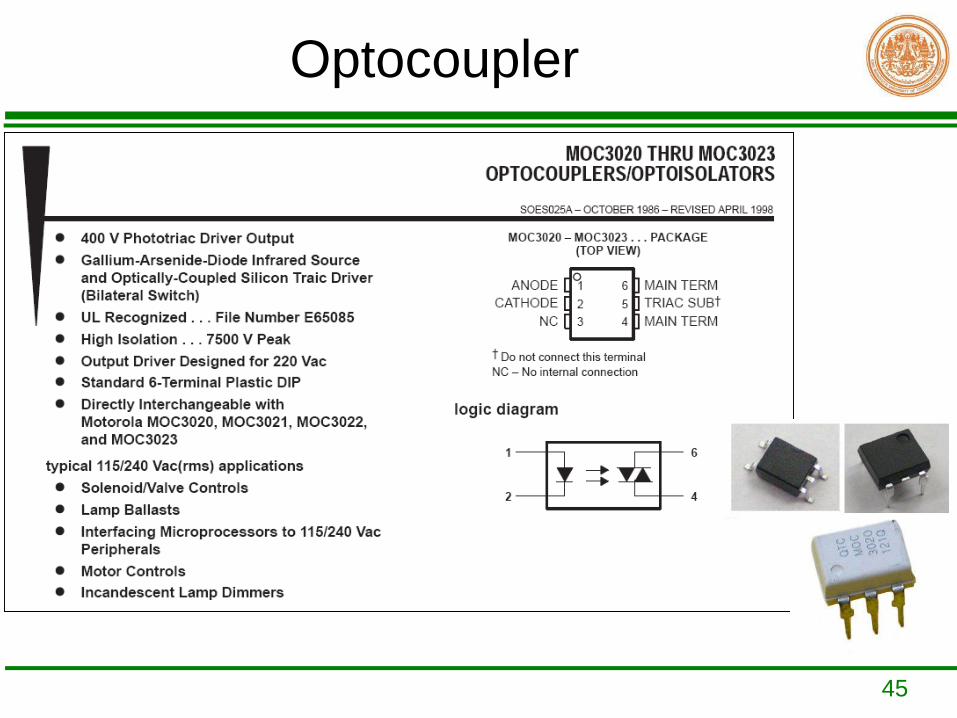
Isolated drive circuit
• For a safety consideration, an isolation between control circuit(low voltage, i.e. 5V triggering pulse) and power circuit(high voltage, i.e. 220V-few kV power plant) is very necessary. The isolation circuit prevents a damage of expensive devices used in control part. The isolation circuit can be implemented by Optoisolator and Transformer.
Optocoupler/Optoisolator
Control Circuit
Power Circuit
45
Optocoupler

46
Example
Snubber Circuit
For Sensitive
gate(Optional)
Note: This opto-isolator/driver should not be used to drive a load directly. It is
intended to be a trigger for power device.
Snubber Circuit
Limit IF(LED input current)