2020 Senior Circuit Pitchers' Combined Ratings and Stamina ...
Caution: Observe precautions when handling because these devices are sensitive to electrostatic discharge.
3 V, SUPER MINIMOLD SILICON MMIC
WIDEBAND AMPLIFIER FOR MOBILE COMMUNICATIONS
BIPOLAR ANALOG INTEGRATED CIRCUIT
PC2745TB,PC2746TB
The mark shows major revised points. Document No. PU10443EJ01V0DS (1st edition) (Previous No. P11511EJ3V0DS00) Date Published November 2003 CP(K)
DESCRIPTION
The PC2745TB and PC2746TB are silicon monolithic integrated circuits designed as buffer amplifier for mobile
communications. These low current amplifiers operate on 3.0 V (1.8 V MIN.).
These ICs are manufactured using our 20 GHz fT NESATIII silicon bipolar process. This process uses silicon
nitride passivation film and gold electrodes. These materials can protect chip surface from external pollution and
prevent corrosion/migration. Thus, these IC have excellent performance, uniformity and reliability.
FEATURES
• Supply voltage : Recommended VCC = 2.7 to 3.3 V
Circuit operation VCC = 1.8 to 3.3 V
• Upper limit operating frequency : PC2745TB; fu = 2.7 GHz TYP.@3 dB bandwidth
PC2746TB; fu = 1.5 GHz TYP.@3 dB bandwidth
• High isolation : PC2745TB; ISL = 38 dB TYP.@f = 500 MHz
PC2746TB; ISL = 45 dB TYP.@f = 500 MHz
• Power gain : PC2745TB; GP = 12 dB TYP.@f = 500 MHz
PC2746TB; GP = 19 dB TYP.@f = 500 MHz
• Saturated output power : PC2745TB; PO(sat) = 1 dBm TYP.@f = 500 MHz
PC2746TB; PO(sat) = 0 dBm TYP.@f = 500 MHz
• High-density surface mounting : 6-pin super minimold package (2.0 1.25 0.9 mm)
APPLICATIONS
• 1.5 GHz to 2.5 GHz communication system : PC2745TB
• 800 MHz to 900 MHz communication system : PC2746TB
ORDERING INFORMATION
Part Number Package Marking Supplying Form
PC2745TB-E3-A 6-pin super minimold C1Q • Embossed tape 8 mm wide
• 1, 2, 3 pins face the perforation side of the tape
• Qty 3 kpcs/reelPC2746TB-E3-A C1R
Remark To order evaluation samples, contact your nearby sales office.
Part number for sample order: PC2745TB-A, PC2746TB-A PHASE-OUT
Data Sheet PU10443EJ1V0DS 2
PC2745TB,PC2746TB
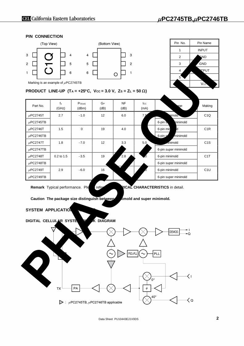
PIN CONNECTION
Pin No. Pin Name
1 INPUT
2 GND
3 GND
4 OUTPUT
5 GND
6 VCC
PRODUCT LINE-UP (TA = +25C, VCC = 3.0 V, ZS = ZL = 50 )
Part No. fu
(GHz)
PO(sat)
(dBm)
GP
(dB)
NF
(dB)
ICC
(mA) Package Making
PC2745T 2.7 1.0 12 6.0 7.5 6-pin minimold C1Q
PC2745TB 6-pin super minimold
PC2746T 1.5 0 19 4.0 7.5 6-pin minimold C1R
PC2746TB 6-pin super minimold
PC2747T 1.8 7.0 12 3.3 5.0 6-pin minimold C1S
PC2747TB 6-pin super minimold
PC2748T 0.2 to 1.5 3.5 19 2.8 6.0 6-pin minimold C1T
PC2748TB 6-pin super minimold
PC2749T 2.9 6.0 16 4.0 6.0 6-pin minimold C1U
PC2749TB 6-pin super minimold
Remark Typical performance. Please refer to ELECTRICAL CHARACTERISTICS in detail.
Caution The package size distinguish between minimold and super minimold.
SYSTEM APPLICATION EXAMPLE
DIGITAL CELLULAR SYSTEM BLOCK DIAGRAM
Marking is an example of PC2745TB
PHASE-OUT
Data Sheet PU10443EJ1V0DS 3
PC2745TB,PC2746TB
PIN EXPLANATION
Pin
No. Pin Name
Applied
Voltage
(V)
Pin
Voltage
(V)Note
Function and Applications Internal Equivalent Circuit
1 INPUT 0.87 Signal input pin. A internal matching
circuit, configured with resistors, enables
50 connection over a wide band. this
pin must be coupled to signal source with
capacitor for DC cut.
0.82
2
3
5
GND 0 Ground pin. This pin should be connected
to system ground with minimum
inductance. Ground pattern on the board
should be formed as wide as possible. All
the ground pins must be connected
together with wide ground pattern to
decrease impedance difference.
4 OUTPUT 1.95 Signal output pin. A internal matching
circuit, configured with resistors, enables
50 connection over a wide band. This
pin must be coupled to next stage with
capacitor for DC cut.
2.54
6 VCC 2.7 to
3.3
Power supply pin. This pin should be
externally equipped with bypass capacity to
minimize ground impedance.
Note Pin voltage is measured at VCC = 3.0 V. Above: PC2745TB, Below: PC2746TB
PHASE-OUT

Data Sheet PU10443EJ1V0DS 4
PC2745TB,PC2746TB
ABSOLUTE MAXIMUM RATINGS
Parameter Symbol Conditions Ratings Unit
Supply Voltage VCC TA = +25C 4.0 V
Circuit Current ICC TA = +25C 16 mA
Power Dissipation PD TA = +85C Note 270 mW
Operating Ambient Temperature TA 40 to +85 C
Storage Temperature Tstg 55 to +150 C
Input Power Pin TA = +25C 0 dBm
Note Mounted on double-sided copper-clad 50 50 1.6 mm epoxy glass PWB
RECOMMENDED OPERATING RANGE
Parameter Symbol MIN. TYP. MAX. Unit
Supply Voltage VCC 2.7 3.0 3.3 V
ELECTRICAL CHARACTERISTICS
(TA = +25C, VCC = 3.0 V, ZS = ZL = 50 , unless otherwise specified)
Parameter Symbol Test Conditions PC2745TB PC2746TB
Unit MIN. TYP. MAX. MIN. TYP. MAX.
Circuit Current ICC No signal 5.0 7.5 10.0 5.0 7.5 10.0 mA
Power Gain GP f = 500 MHz 9 12 14 16 19 21 dB
Noise Figure NF f = 500 MHz 6.0 7.5 4.0 5.5 dB
Upper Limit Operating Frequency fu 3 dB down below
from gain at f =
0.1 GHz
2.3 2.7 1.1 1.5 GHz
Isolation ISL f = 500 MHz 33 38 40 45 dB
Input Return Loss RLin f = 500 MHz 8 11 10 13 dB
Output Return Loss RLout f = 500 MHz 2.5 5.5 5.5 8.5 dB
Saturated Output Power PO(sat) f = 500 MHz,
Pin = 6 dBm
4.0 1.0 3.0 0 dBm
PHASE-OUT

Data Sheet PU10443EJ1V0DS 5
PC2745TB,PC2746TB
STANDARD CHARACTERISTICS FOR REFERENCE (TA = +25C, VCC = 3.0 V, ZS = ZL = 50 )
Parameter Symbol Test Conditions Reference Value Unit
PC2745TB PC2746TB
Circuit Current ICC VCC = 1.8 V, No signal 4.5 4.5 mA
Power Gain GP VCC = 3.0 V, f = 1.0 GHz
VCC = 3.0 V, f = 2.0 GHz
VCC = 1.8 V, f = 0.5 GHz
12.0
11.0
7.0
18.5
14.0
dB
Noise Figure NF VCC = 3.0 V, f = 1.0 GHz
VCC = 3.0 V, f = 2.0 GHz
VCC = 1.8 V, f = 0.5 GHz
5.5
5.7
8.0
4.2
5.0
dB
Upper Limit
Operating
Frequency
fu VCC = 1.8 V, 3 dB down below from gain at f = 0.1 GHz 1.8 1.1 GHz
Isolation ISL VCC = 3.0 V, f = 1.0 GHz
VCC = 3.0 V, f = 2.0 GHz
VCC = 1.8 V, f = 0.5 GHz
33
30
35
38
37
dB
Input Return
Loss
RLin VCC = 3.0 V, f = 1.0 GHz
VCC = 3.0 V, f = 2.0 GHz
VCC = 1.8 V, f = 0.5 GHz
13.0
14.0
6.5
10.0
10.0
dB
Output Return
Loss
RLout VCC = 3.0 V, f = 1.0 GHz
VCC = 3.0 V, f = 2.0 GHz
VCC = 1.8 V, f = 0.5 GHz
6.5
8.5
6.0
8.5
9.5
dB
Saturated
Output Power
PO(sat) VCC = 3.0 V, f = 1.0 GHz, Pin = 6 dBm
VCC = 3.0 V, f = 2.0 GHz, Pin = 6 dBm
VCC = 1.8 V, f = 0.5 GHz, Pin = 10 dBm
2.5
3.5
11.0
1.0
8.0
dBm
3rd Order
Intermodulation
Distortion
IM3 VCC = 3.0 V, Pout = 10 dBm, f1 = 500 MHz, f2 = 502 MHz
VCC = 1.8 V, Pout = 20 dBm, f1 = 500 MHz, f2 = 502 MHz
VCC = 3.0 V, Pout = 10 dBm, f1 = 1 000 MHz, f2 = 1 002 MHz
30.0
31.0
26.0
26.0
37.0
dBc
PHASE-OUT
Data Sheet PU10443EJ1V0DS 6
PC2745TB,PC2746TB
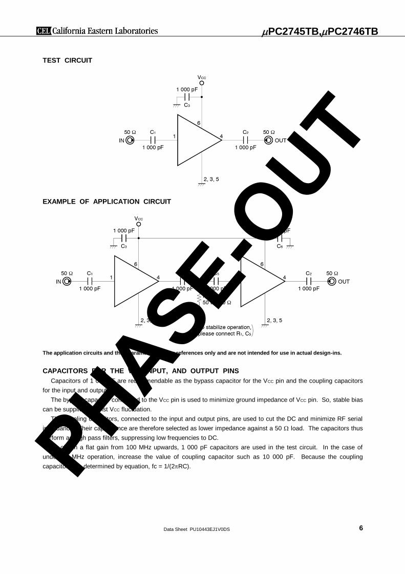
TEST CIRCUIT
EXAMPLE OF APPLICATION CIRCUIT
The application circuits and their parameters are for references only and are not intended for use in actual design-ins.
CAPACITORS FOR THE VCC, INPUT, AND OUTPUT PINS
Capacitors of 1 000 pF are recommendable as the bypass capacitor for the VCC pin and the coupling capacitors
for the input and output pins.
The bypass capacitor connected to the VCC pin is used to minimize ground impedance of VCC pin. So, stable bias
can be supplied against VCC fluctuation.
The coupling capacitors, connected to the input and output pins, are used to cut the DC and minimize RF serial
impedance. Their capacitance are therefore selected as lower impedance against a 50 load. The capacitors thus
perform as high pass filters, suppressing low frequencies to DC.
To obtain a flat gain from 100 MHz upwards, 1 000 pF capacitors are used in the test circuit. In the case of
under 10 MHz operation, increase the value of coupling capacitor such as 10 000 pF. Because the coupling
capacitors are determined by equation, fc = 1/(2RC).
PHASE-OUT
Data Sheet PU10443EJ1V0DS 7
PC2745TB,PC2746TB
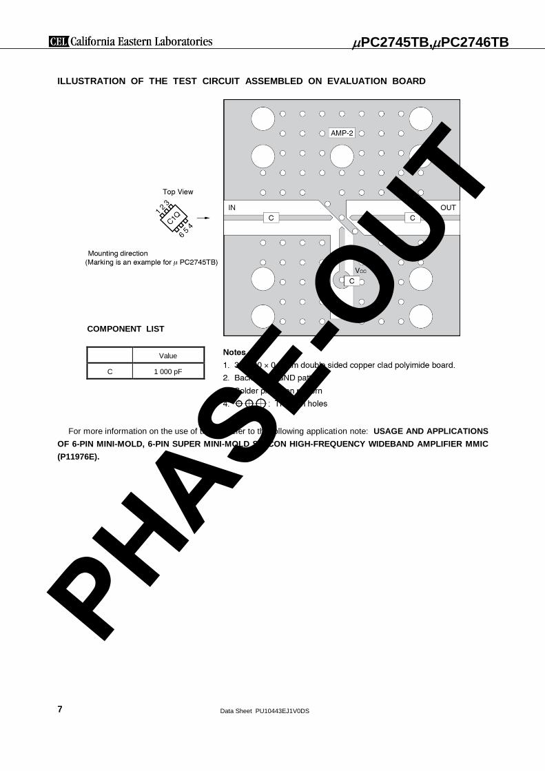
ILLUSTRATION OF THE TEST CIRCUIT ASSEMBLED ON EVALUATION BOARD
For more information on the use of this IC, refer to the following application note: USAGE AND APPLICATIONS
OF 6-PIN MINI-MOLD, 6-PIN SUPER MINI-MOLD SILICON HIGH-FREQUENCY WIDEBAND AMPLIFIER MMIC
(P11976E).
COMPONENT LIST
Value
C 1 000 pF
PHASE-OUT
Data Sheet PU10443EJ1V0DS 8
PC2745TB,PC2746TB
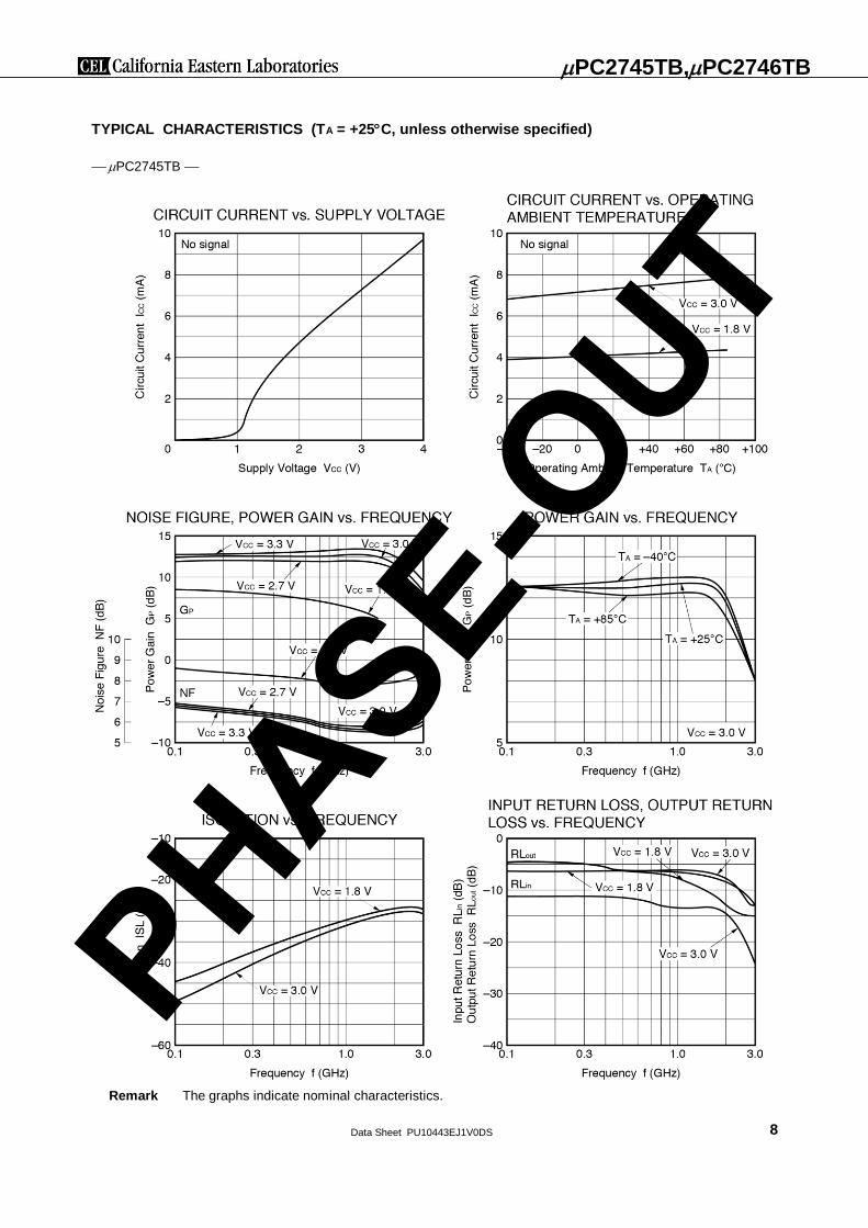
TYPICAL CHARACTERISTICS (TA = +25C, unless otherwise specified)
PC2745TB
Remark The graphs indicate nominal characteristics.
PHASE-OUT

Data Sheet PU10443EJ1V0DS 9
PC2745TB,PC2746TB
PC2745TB
Remark The graphs indicate nominal characteristics.
PHASE-OUT

Data Sheet PU10443EJ1V0DS 10
PC2745TB,PC2746TB
SMITH CHART (TA = +25C, VCC = 3.0 V)
PC2745TB
S11-FREQUENCY
S22-FREQUENCY
PHASE-OUT
Data Sheet PU10443EJ1V0DS 11
PC2745TB,PC2746TB
S-PARAMETERS
PHASE-OUT

Data Sheet PU10443EJ1V0DS 12
PC2745TB,PC2746TB
TYPICAL CHARACTERISTICS (TA = +25C, unless otherwise specified)
PC2746TB
Remark The graphs indicate nominal characteristics.
PHASE-OUT

Data Sheet PU10443EJ1V0DS 13
PC2745TB,PC2746TB
PC2746TB
Remark The graphs indicate nominal characteristics.
PHASE-OUT
Data Sheet PU10443EJ1V0DS 14
PC2745TB,PC2746TB
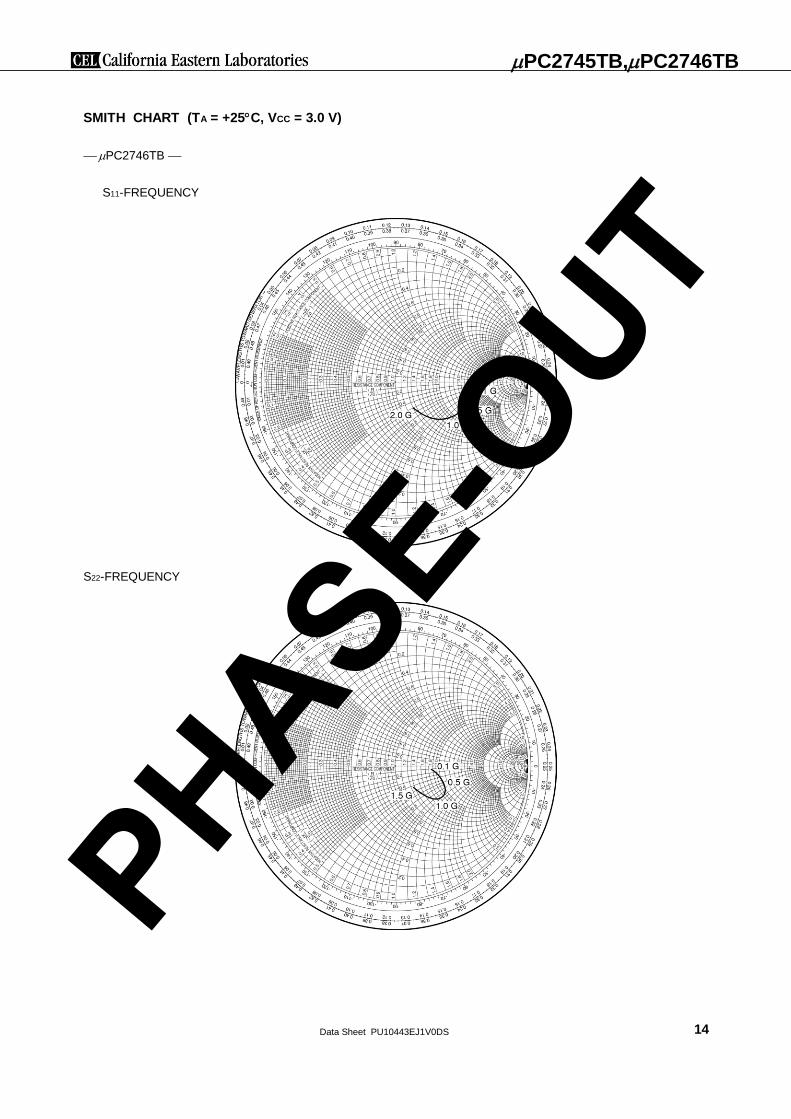
SMITH CHART (TA = +25C, VCC = 3.0 V)
PC2746TB
S11-FREQUENCY
S22-FREQUENCY
PHASE-OUT

Data Sheet PU10443EJ1V0DS 15
PC2745TB,PC2746TB
S-PARAMETERS
PHASE-OUT

Data Sheet PU10443EJ1V0DS 16
PC2745TB,PC2746TB
PACKAGE DIMENSIONS
6-PIN SUPER MINIMOLD (UNIT: mm)
PHASE-OUT
Data Sheet PU10443EJ1V0DS 17
PC2745TB,PC2746TB
NOTES ON CORRECT USE
(1) Observe precautions for handling because of electro-static sensitive devices.
(2) Form a ground pattern as widely as possible to minimize ground impedance (to prevent undesired oscillation).
All the ground pins must be connected together with wide ground pattern to decrease impedance difference.
(3) The bypass capacitor should be attached to the VCC pin.
(4) The DC cut capacitor must be attached to input pin and output pin.
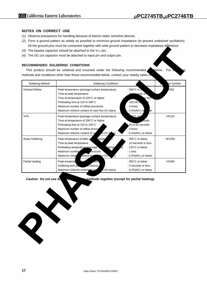
RECOMMENDED SOLDERING CONDITIONS
This product should be soldered and mounted under the following recommended conditions. For soldering
methods and conditions other than those recommended below, contact your nearby sales office.
Soldering Method Soldering Conditions Condition Symbol
Infrared Reflow Peak temperature (package surface temperature) : 260C or below
Time at peak temperature : 10 seconds or less
Time at temperature of 220C or higher : 60 seconds or less
Preheating time at 120 to 180C : 12030 seconds
Maximum number of reflow processes : 3 times
Maximum chlorine content of rosin flux (% mass) : 0.2%(Wt.) or below
IR260
VPS Peak temperature (package surface temperature) : 215C or below
Time at temperature of 200C or higher : 25 to 40 seconds
Preheating time at 120 to 150C : 30 to 60 seconds
Maximum number of reflow processes : 3 times
Maximum chlorine content of rosin flux (% mass) : 0.2%(Wt.) or below
VP215
Wave Soldering Peak temperature (molten solder temperature) : 260C or below
Time at peak temperature : 10 seconds or less
Preheating temperature (package surface temperature) : 120C or below
Maximum number of flow processes : 1 time
Maximum chlorine content of rosin flux (% mass) : 0.2%(Wt.) or below
WS260
Partial Heating Peak temperature (pin temperature) : 350C or below
Soldering time (per side of device) : 3 seconds or less
Maximum chlorine content of rosin flux (% mass) : 0.2%(Wt.) or below
HS350
Caution Do not use different soldering methods together (except for partial heating).
PHASE-OUT
NOTICE
1. Descriptions of circuits, software and other related information in this document are provided only to illustrate the operation of semiconductor products and application examples. You are fully responsible for the incorporation of these circuits, software, and information in the design of your equipment. California Eastern Laboratories and Renesas Electronics assumes no responsibility for any losses incurred by you or third parties arising from the use of these circuits, software, or information.
2. California Eastern Laboratories has used reasonable care in preparing the information included in this document, but California Eastern Laboratories does not warrant that such information is error free. California Eastern Laboratories and Renesas Electronics assumes no liability whatsoever for any damages incurred by you resulting from errors in or omissions from the information included herein.
3. California Eastern Laboratories and Renesas Electronics do not assume any liability for infringement of patents, copyrights, or other intellectual property rights of third parties by or arising from the use of Renesas Electronics products or technical information described in this document. No license, express, implied or otherwise, is granted hereby under any patents, copyrights or other intellectual property rights of California Eastern Laboratories or Renesas Electronics or others.
4. You should not alter, modify, copy, or otherwise misappropriate any Renesas Electronics product, whether in whole or in part. California Eastern Laboratories and Renesas Electronics assume no responsibility for any losses incurred by you or third parties arising from such alteration, modification, copy or otherwise misappropriation of Renesas Electronics product.
5. Renesas Electronics products are classified according to the following two quality grades: “Standard” and “High Quality”. The recommended applications for each Renesas Electronics product depends on the product’s quality grade, as indicated below. “Standard”: Computers; office equipment; communications equipment; test and measurement equipment; audio and visual equipment; home electronic appliances; machine tools; personal electronic equipment; and industrial robots etc. “High Quality”: Transportation equipment (automobiles, trains, ships, etc.); traffic control systems; anti-disaster systems; anti-crime systems; and safety equipment etc. Renesas Electronics products are neither intended nor authorized for use in products or systems that may pose a direct threat to human life or bodily injury (artificial life support devices or systems, surgical implantations etc.), or may cause serious property damages (nuclear reactor control systems, military equipment etc.). You must check the quality grade of each Renesas Electronics product before using it in a particular application. You may not use any Renesas Electronics product for any application for which it is not intended. California Eastern Laboratories and Renesas Electronics shall not be in any way liable for any damages or losses incurred by you or third parties arising from the use of any Renesas Electronics product for which the product is not intended by California Eastern Laboratories or Renesas Electronics.
6. You should use the Renesas Electronics products described in this document within the range specified by California Eastern Laboratories, especially with respect to the maximum rating, operating supply voltage range, movement power voltage range, heat radiation characteristics, installation and other product characteristics. California Eastern Laboratories shall have no liability for malfunctions or damages arising out of the use of Renesas Electronics products beyond such specified ranges.
7. Although Renesas Electronics endeavors to improve the quality and reliability of its products, semiconductor products have specific characteristics such as the occurrence of failure at a certain rate and malfunctions under certain use conditions. Further, Renesas Electronics products are not subject to radiation resistance design. Please be sure to implement safety measures to guard them against the possibility of physical injury, and injury or damage caused by fire in the event of the failure of a Renesas Electronics product, such as safety design for hardware and software including but not limited to redundancy, fire control and malfunction prevention, appropriate treatment for aging degradation or any other appropriate measures. Because the evaluation of microcomputer software alone is very difficult, please evaluate the safety of the final products or systems manufactured by you.
8. Please contact a California Eastern Laboratories sales office for details as to environmental matters such as the environmental compatibility of each Renesas Electronics product. Please use Renesas Electronics products in compliance with all applicable laws and regulations that regulate the inclusion or use of controlled substances, including without limitation, the EU RoHS Directive. California Eastern Laboratories and Renesas Electronics assume no liability for damages or losses occurring as a result of your noncompliance with applicable laws and regulations.
9. Renesas Electronics products and technology may not be used for or incorporated into any products or systems whose manufacture, use, or sale is prohibited under any applicable domestic or foreign laws or regulations. You should not use Renesas Electronics products or technology described in this document for any purpose relating to military applications or use by the military, including but not limited to the development of weapons of mass destruction. When exporting the Renesas Electronics products or technology described in this document, you should comply with the applicable export control laws and regulations and follow the procedures required by such laws and regulations.
10. It is the responsibility of the buyer or distributor of California Eastern Laboratories, who distributes, disposes of, or otherwise places the Renesas Electronics product with a third party, to notify such third party in advance of the contents and conditions set forth in this document, California Eastern Laboratories and Renesas Electronics assume no responsibility for any losses incurred by you or third parties as a result of unauthorized use of Renesas Electronics products.
11. This document may not be reproduced or duplicated in any form, in whole or in part, without prior written consent of California Eastern Laboratories.12. Please contact a California Eastern Laboratories sales office if you have any questions regarding the information contained in this document or Renesas
Electronics products, or if you have any other inquiries.
NOTE 1: “Renesas Electronics” as used in this document means Renesas Electronics Corporation and also includes its majority-owned subsidiaries.NOTE 2: “Renesas Electronics product(s)” means any product developed or manufactured by or for Renesas Electronics.NOTE 3: Products and product information are subject to change without notice.
CEL Headquarters • 4590 Patrick Henry Drive, Santa Clara, CA 95054 • Phone (408) 919-2500 • www.cel.com
For a complete list of sales offices, representatives and distributors,Please visit our website: www.cel.com/contactusPHASE-O
UT