
BEOL Interconnect Innovations for Improving Performance · PDF fileBEOL Interconnect...
35
BEOL Interconnect Innovations for Improving Performance Paul Besser, PhD Formerly Senior Technology Director at Lam Research Currently Director of Emerging Technologies at ARM February 23, 2017 Paul Besser, NCCAVS Symposium in San Jose, CA
Transcript of BEOL Interconnect Innovations for Improving Performance · PDF fileBEOL Interconnect...

BEOL Interconnect Innovations for Improving Performance
Paul Besser, PhD
Formerly Senior Technology Director at Lam Research
Currently Director of Emerging Technologies at ARM
February 23, 2017 Paul Besser, NCCAVS Symposium in San Jose, CA

Acknowledgements
• Lam Research • Hui-Jung Wu, Justin Jiang, Kaushik Chattopadhyay, Lee Brogan, Natalia Doubina, Nagraj
Shankar, Cheng-Kai Li, and Larry Zhao
• imec • Houman Zahedmanesh, Kristof Croes, Ivan Ciofi
• GLOBALFOUNDRIES • Todd Ryan
• ARM • Saurabh Sinha, Brian Cline, Greg Yeric
February 23, 2017 Paul Besser, NCCAVS Symposium in San Jose, CA 2

Market Needs Drive Requirements and Technology Innovations
3
• Power, performance, cost/area (PPA) are driving our industry
• Customers demand the highest performing processors
Performance Power Cost/Area
Slide from Paul Besser, Semicon Korea 2014
A4 A5 A6 A7 A8 A9
32nm HKMG 28nm HKMG 20nm HKMG 14nm FinFET
February 23, 2017 Paul Besser, NCCAVS Symposium in San Jose, CA

Innovations in Silicon Manufacturing
February 23, 2017 Paul Besser, NCCAVS Symposium in San Jose, CA 4
11 Elements
+4 Elements
+45 Elements (Potential)
New materials enable innovation by Improving performance, Enabling dimensional scaling, and Improving reliability
Slide from Paul Besser, Semicon Korea 2014

Eless Co via prefill
Co metal
Air gap at tight pitch
New Cu BM
Eless Ni
MOL and BEOL Materials Innovations Roadmap
• Improving performance (data access speed, battery life, etc.) is much more than just shrinking the dimensions of the processor
• Novel materials innovations drive contact and BEOL RC improvement (reduction) • RC Delay ∝ Resistance x Capacitance
Al wires
ILD Cu caps
FTEOS ILD
Low-K ILD
CoWP cap
CPI Low-K ESL
Ultra low K
ULK cap
Cu contact
Dual Si2
Porous LK
Cu alloys
ELD Cu
MIS
TiSix
Air Gap
Selective metal caps
Porous LK
CVD Co
AlN ESL
TiSi2
ALD W
NiPtSi
Technology Node (nm)
350 250 180/130 90 65 /45 45/32 28/20 14 /10 7/5 nm
BEOL Contacts
New BM
Co metals
FTEOS ILD
Cu barriers
Cu wiring
CVD W
MOCVD TiN
CoSI2
February 23, 2017 Paul Besser, NCCAVS Symposium in San Jose, CA 5 Besser, ECS Prime, October 2016

BEOL — How Important Are Resistance and Capacitance?
• Back-end interconnect resistance will dominate product performance at 5nm
• BEOL capacitance scaling slows, beyond 10nm
Greg Yeric, ARM (IEDM 2014)
Key issue at 5 nm: non-scaling parasitics
Line Rs dominates but at 5 nm
Via Rs will affect design
More power is required when design adds a buffer to compensate for R
Unidirectional patterning has made via Rs more critical since it requires routing changes; standard cell routes must go through multiple vias B
EO
L
F
EO
L
February 23, 2017 Paul Besser, NCCAVS Symposium in San Jose, CA 6
James Hsueh-Chung Chen (IITC 2014)
Besser, ECS Prime, October 2016

BEOL RC Reduction Innovations for Future Generations
• How to reduce C • New lower K dielectrics, even dielectric replacement
• Air gaps
• Lower K ESL
• How to reduce R • New metals
• Reduce barrier thickness
• Reduce barrier metal resistivity
RC Delay ∝ Resistance x Capacitance
Al Wires
ILD Cu caps
FTEOS ILD
Low K ILD
CoWP cap
CPI Low-K ESL
Ultra Low-K
ULK Cap
Cu Contact
Dual Si2
Porous LK
Cu Alloys
ELD Cu
TiSi2
ALD W
NiPtSi
Technology Node (nm)
350 250 180/130 90 65 /45 45/32 28/20 14 10/7 nm
FTEOS ILD
Cu Barriers
Cu wiring
CVD W
MOCVD TiN
CoSI2
Eless Co via prefill
Co Metal
Air gap at tight pitch
New Cu BM
Eless Ni
MIS
TiSix
Air Gap
Selective Metal caps
Porous LK
CVD Co
AlN ESL
BEOL Contacts
New BM
Co Metals
February 23, 2017 Paul Besser, NCCAVS Symposium in San Jose, CA 7 Besser, ECS Prime, October 2016

Capacitance Reduction Opportunities
February 23, 2017 Paul Besser, NCCAVS Symposium in San Jose, CA 8

Challenges with Lowering Capacitance
• Capacitance (C) can be reduced by lowering the dielectric constant (k) of the material, but at a cost! • Dielectric constant is lowered by changing the chemical composition of the dielectric or by introducing
porosity (pULK)**
• i k will i elastic modulus (E) reliability, integration, and packaging issues
• Process-induced damage to trench sidewall and top interface is a major integration challenge** • Higher K, moisture uptake, increased capacitance, TDDB failure
** Alfred Grill et al. Appl Phys Rev 1, 011306 (2014)
February 23, 2017 Paul Besser, NCCAVS Symposium in San Jose, CA 9
P.R. Besser, ECS Trans 2(6), 3 (2007)

TDDB Lifetime and Interconnect Scaling
• Capacitance reduction by increasing porosity is high risk with little benefit • TDDB is a critical hurdle for BEOL scaling, suffering an order of magnitude degradation for each generation
@ ULK2.4 • Reducing ULK dielectric constant further degrades dielectric reliability • Poor LER and misaligned vias can further degrade TDDB
S.-C. Lee, (TSMC) IRPS 2014
“Progress in lowering k, or even maintaining it at present levels, with continued technology
progression requires integration of (novel) non-porous materials or changes in interconnect
architecture to include air-gaps.”* *A. Oates (TSMC) IEDM 2014
TDDB lifetime as a function of spacing with ULK2.4
G. Bonilla, et al (IBM/GF), IRPS 2011 E. V. Besien (IMEC), AMC, 2010
February 23, 2017 Paul Besser, NCCAVS Symposium in San Jose, CA 10 Slide from Besser, ECS Prime, October 2016

New Dielectrics Can Help Reduce RC, but Have Challenges
• Porous low k were introduced as part of the 32/28 nm technology
• h porosity i k value, but dielectrics have h process-induced damage and i mechanical strength
• Damage h the effective k and can erase the capacitance benefit
• As a result, at tight pitch interconnects, industry options are ** • Higher K, non-porous, dense LK dielectrics (less susceptible to damage)
• Single precursor formulations (dense LK) with a lower K, and/or
• Low porosity ULK with higher C content
• Industry is spending much resource and has a huge risk exposure for a little gain in C • Is there a better way?
** E Todd Ryan et al, IITC-MAM (2015) Rama Divakaruni (IBM) SOI Technology Summit, Shanghai (2013)
February 23, 2017 Paul Besser, NCCAVS Symposium in San Jose, CA 11

Technology Elements of Air Gaps (AG) in Integrated Circuits
• Air gap insertion has been demonstrated to reduce capacitance and lower the effective dielectric constant • Logic had AG >20 years ago: Al technology, pre-unlanded vias
• Memory AG in production for years: NAND BL-BL + WL-WL, DRAM BL-BL
• AG for capacitance reduction reemerging ** • Implemented by Intel 14 nm in performance critical layers
• Two metal levels, with one level without air gap between AG layers
• Huge RC gain was realized – 14 and 17% at 80 and 160nm pitch.
February 23, 2017 Paul Besser, NCCAVS Symposium in San Jose, CA 12
Fischer et al., IITC/MAM (2015)
G Schindler et al., AMC (2006)
** Intel, IEDM (2014)

Air Gap Structure and Integration Flow
1. Diffusion barrier open in select AG
regions
2. Low-k etch process
3. Post-etch strip/clean
4. Conformal dielectric barrier
deposition
5. Non-conformal low-k deposition to
create AG
Every process step is critical for reliability, but conformal DB dep affects design
February 23, 2017 Paul Besser, NCCAVS Symposium in San Jose, CA 13

Reliability Considerations: Short Lines are Integrated in Products!
• Under normal electromigration (EM) testing, • As atoms diffuse along the line length, compressive and tensile stresses develop at opposite
ends of the line
• Line length: • If the line is long, then a void develops in the line = failure
• If the line is short enough (< jLcrit), there is a balance between electromigration- and stress-induced atomic diffusion
• Short-line effect: • Short lines will never fail (< jLcrit = Blech Length)
• Short-line effect will depend on dielectric material**
electrons
0.7
1.2
1.7
2.2
1
Distance
Stress
DEM
Dstress
**Hau-Riege et al., J. Appl. Phys. 96, 5792 (2004)
February 23, 2017 Paul Besser, NCCAVS Symposium in San Jose, CA 14
Designers utilize and rely on short line effects in their designs for tight pitch interconnects; however,
Blech Length is also considered at all metal layers, for deciding current density design rules

Thickness of DB, Post Air Gap Formation, Affects Reliability
• Air gaps have to be designed into the chip • Air gaps are selectively introduced, avoiding vias and placing air gaps at
critical layers with high current densities for maximum benefit
• Process-oriented simulations reveal affect of Air Gaps on circuit design: • As expected, the tensile stress in Cu lines increases
linearly DB thickness
• Jlcrit (Blech Length) in an air-gapped interconnect depends on SiCN (DB) thickness and increasing the DB thickness degrades Jlcrit
• Airgapped interconnects with 5 nm conformal SiCN have a Jlcrit comparable to non-airgapped interconnects (with ULK 2.5 ILD)
• DB must be thick enough to be hermetic, but if too thick, Jlcrit will be degraded, affecting circuit design
February 23, 2017 Paul Besser, NCCAVS Symposium in San Jose, CA 15
Houman, Besser, Wilson and Croes, JAP 120, 095103 (2016)

Dielectric Barrier/Etch Stop Layer Requirements
• Requirements for dielectric barrier/ESL • Cu diffusion barrier
• Hermetic barrier for moisture and O2
• High etch selectivity
• Excellent adhesion to metal and ULK
• High breakdown voltage and low leakage
• Low dielectric constant
• A combination of high etch selectivity ESL and thin hermetic Cu barrier enables DB scaling
• A high selectivity ESL can provide better control of unlanded via over etch and enable TiN wet removal with protected via bottom • Replacing SiCN with AlN + SiCO is a offers a highly conformal stack with high etch
selectivity, keff reduction, and excellent diffusion barrier;
• film is hermetic at 3 nm thick.
February 23, 2017 Paul Besser, NCCAVS Symposium in San Jose, CA 16
Thicker Barrier
Slide from Paul Besser, ECS (2016)

Dielectric Barrier (DB)/Etch Stop Layer (ESL) Scaling to the Rescue
• Modelling suggest thinning or scaling the DB to 5 nm NDC thickness provides 7% keff reduction, which is more than one generation of low k dielectric progress.
• Can DB/ESL continue to scale with all the DB/ESL requirements and increasing complex patterning?
Intel
tsmc
SEC 14 nm
18nm SiO2
18nm SiCN
Samsung
February 23, 2017 Paul Besser, NCCAVS Symposium in San Jose, CA 17 Slide from Paul Besser, ECS (2016)

Dielectric Barrier (DB)/Etch Stop Layer (ESL) Scaling to the Rescue
• DB/ESL remains as the key process for capacitance reduction
• Co-optimization of etch and ESL is needed to enable robust via patterning and capacitance improvement
February 23, 2017 Paul Besser, NCCAVS Symposium in San Jose, CA 18
• Integrating AlN + SiCO stacks as a replacement for SiCN provides an integration advantage:
• Scaling enabled
• High etch selectivity
• Significant keff reduction
• Excellent diffusion barrier
Slide from Paul Besser, ECS (2016)

Resistance Reduction Opportunities How far can Cu extend? And what replaces Cu?
February 23, 2017 Paul Besser, NCCAVS Symposium in San Jose, CA 19

Understanding Copper Resistance Increase in Narrow Features
• Resistance increase with decreasing linewidth, due to scattering • Electrons are scattered by grain boundaries, interfaces, surfaces, and defects (Cu electron
mfp = 36 nm)
• Scattering events lead to Cu resistivity h with i linewidth
• How to compensate? • Increase aspect ratio of the Cu line? Void-free fill is a challenge.
P.R. Besser, ECS Trans 2(6), 3 (2007) W. Steinhogl et al., Phys Rev B66 (2002) G. Schindler, Sematech workshop on Cu resistivity (2005)
February 23, 2017 Paul Besser, NCCAVS Symposium in San Jose, CA 20

Why Line Resistance Increases as Linewidth Decreases
• Cu extendibility is challenged by fill, barrier integrity, conductive metal area, and scattering; Cu current carrying cross-section i with i linewidth
• A calculation of conductive metal area and Cu line Rs as a function of linewidth reveals • Barrier thicknesses has not scaled below 2.5 nm, but must scale for Cu to scale below 20 nm linewidth, and
• Area for conductive metal is small, leading to a high Rs in narrow features
February 23, 2017 Paul Besser, NCCAVS Symposium in San Jose, CA 21
TaN = 1000 µOhm-cm
Co = 15-21 µOhm-cm
Cu = 4-15 µOhm-cm
NOT dawn to scale
Slide from Paul Besser, ECS (2016)

BEOL Scaling Simulations: Cu can Extend to 7 nm, Maybe to 5 nm
PVD TaN barrier + CVD Co liner
PVD TaN barrier + CVD Co liner + PVD Cu seed
PVD TaN/Ta barrier + PVD Cu seed
► CoventorTM simulations (to scale) reveal the challenge with extending PVD barrier/liner/seed: PVD overhang and can lead to voids in narrow features
Cu extendibility is a function of design rules
Cu seed extendibility to 5nm is questionable
► Migrating to PVD TaN/CVD liner (Co or Ru) is likely at 7 nm to enable extendibility of Cu
February 23, 2017 Paul Besser, NCCAVS Symposium in San Jose, CA 22 Slide from Paul Besser, ECS (2016)
10 nm 7 nm 5 nm

At 10 and 7nm, Cu Extendibility is Possible
• Co liner provides an improvement for Cu scaling; however, only to 12 nm linewidth
• Scaling the liner thickness (with alternative liners) can extend Cu, but with a net resistance line resistance increase
February 23, 2017 Paul Besser, NCCAVS Symposium in San Jose, CA 23
van der Veen, IITC AMC (2016)

What Is Beyond Cu?
February 23, 2017 Paul Besser, NCCAVS Symposium in San Jose, CA 24

Resistivity in Narrow Features (Intel, 2015)
• At the 5 nm node, not scaling the PVD liner thickness reduces the electrical area by a factor of 2 while increasing the Rs by an order of magnitude
• Based on modeling, resistivity in a 12 nm line (AR=1.5, 3 nm liner) is dominated by surface scattering: • Surface scattering (54%), bulk resistivity/phonon(15%) and GB scattering (31%)
• Options to reduce line Rs: • Subtractive patterning
• Scale liner thickness barrierless
• Smaller EMFP metals
February 23, 2017 Paul Besser, NCCAVS Symposium in San Jose, CA 25
Cu
Chawla et al, (AMC 2015)

Another Perspective: EMFP and Resistivity
• In the case of thin wires and/or small grain sizes, the wire resistivity is proportional to the product of EMFP (l) and bulk resistivity (r0), for a fixed grain size distribution and linewidth
• With this metric, options to consider as Cu replacements are: • Rh cost
• Ir cost
• Al cost and thermal excursion
• Co
• Ni options to consider…
• Ru
D. Gall, JAP 119, 085101 (2016)
February 23, 2017 Paul Besser, NCCAVS Symposium in San Jose, CA 26

Metal Options: Choosing a Good Metal Conductor to Replace Cu
Cu Co Ru Ni
Barrier/Liner Needed Barrier Thin liner Thin liner TBD
Bulk Resistivity
EMFP (nm) 39 6 10 18
Melting Point (°C) 1083 1495 2250 1453
Deposition processes ECD, PVD ECD, ELD, CVD, PVD
CVD, PVD PVD, CVD,
ELD
Gap Fill of Narrow Features
Cost
February 23, 2017 Paul Besser, NCCAVS Symposium in San Jose, CA 27 Slide from Besser, ECS Prime, October 2016
Co exhibits short EMFP, high melting point, and can be deposited with various techniques at low cost
P.R. Besser, ECS Trans 2(6), 3 (2007)

Why Cobalt for Interconnects?
• Co is already integrated in IC processing as a liner and a cap layer
• The shorter mean free path of electrons in Co and the reduced requirement for a barrier reduce the resistivity disadvantage of Co (vs. Cu) in the 15-20 nm line dimension range
• Co electromigration (EM) is better than Cu, based on melting point and publications
• Electroplating allows bottom-up Co fill at a low cost, but CVD/PVD also fills features
• IMEC simulations suggest barrierless vias filled with Co have a resistance benefit for N7 and beyond
February 23, 2017 Paul Besser, NCCAVS Symposium in San Jose, CA 28
0
1,000
2,000
3,000
4,000
Al Cu Ni Co Ru W
(°C)
Melting Point vs. Interconnect Metal
M. H. van der Veen et al., IITC (2015) G. J. van Gurp, Thin Solid Films (1976) M. H. van der Veen, IITC/MAM (2015)
Slide from Besser, ECS Prime, October 2016

Enabling Void-Free Metallization with Co Electrochemical Dep
• Co electroplating on CVD Co liner alleviates PVD Cu seed “pinch off”
• Co liner oxidizes when exposed to air and leads to resistivity increase and potential interfacial integrity degradation
• Pre-treatment of Co liner results in substantial conductivity increase and allows for improved nucleation of ECP Co film
• Temperature/time/chemistry can be used to control the sheet resistance drop and Co agglomeration
10 nm 7 nm 5 nm
PVD TaN +
CVD Co liner
PVD TaN +
CVD Co liner +
PVD Cu seed
Natalia Doubina et al., CSTIC 2016, Shanghai
February 23, 2017 Paul Besser, NCCAVS Symposium in San Jose, CA 29
Hui-Jung Wu et al., Semicon West (2016)
Slide from Besser, ECS Prime, October 2016

Other Alternatives to Cu
• Resistance and Electromigration Performance of 6 nm Wires (Intel)
• Line Rs and EM were measured for 6 nm CD wires; interconnect performance was measured down to 60 nm2 wire cross-sectional area.
• Ruthenium is an option to replace Cu at 5nm (imec, GLOBALFOUNDRIES, IBM)
• Ru reflows at a low temperature; resistivity is 18 µΩ-cm at 7 nm LW is better than Cu (with a 2 nm barrier); via Rs was comparable to Cu; a thin adhesion layer is required (TiN), but TDDB and EM are good
• The challenges with Ru are cost, CMP, and immaturity
Chawla et al., IITC/AMC (2016)
Adelman et al., IITC/AMC (2016) Zhang et al., IITC/AMC (2016)
February 23, 2017 Paul Besser, NCCAVS Symposium in San Jose, CA 30 Slide from Besser, ECS Prime, October 2016

How to Reduce Interconnect Rs Further?
• The solutions shown thus far are incremental improvements in via/line Rs: the industry needs still lower via and line Rs!
Contributions to line resistance
A intrinsic resistance of metal = f(material)
B increase in Rs due to scattering = f
(interfaces, grains, impurities, etc)
C increase in Rs due to resistive barriers or
geometry
Low or no barrier/liner offers an
opportunity to eliminate the
increase in Rs due to barriers (C)
NOT drawn to scale
= +
A,B C
February 23, 2017 Paul Besser, NCCAVS Symposium in San Jose, CA 31 Slide from Besser, ECS Prime, October 2016

How to Reduce Interconnect Rs Further?
• The solutions shown thus far are incremental improvements in via/line Rs: the industry needs still lower via and line Rs!
• One option: directly platable, conductive liner • Co-Ti (University of Tokyo). Resistivity is ~130 μΩ-cm
• Co-Mo (Fudan University). Resistivity is 100-150 μΩ-cm
• Co-W (Tokyo University). Resistivity of CoW films (200 nm) with 10 and 20%W were 80 and 200 μΩ-cm. Adding Cp2WH2 into source gas in an ALD cycle -> CoW alloy film with 5%W without including WO3 or C reduced resistivity to 25 μΩ-cm (15 nm thick)
• Co-Si (Literature). Resistivity is10-40 μΩ-cm, depending on the phase of CoSix formed
February 23, 2017 Paul Besser, NCCAVS Symposium in San Jose, CA 32
Li-Ao Cao et al, IITC/AMC 2016 Shimizu et al., J Mater Chem C 2500 (2015)
Co-Ti Co-Mo Co-W Co-Si
M. Hosseini et al., IITC/AMC 2016
Murarka et al, JAP (1984) Prokop et al, Thin Solid Films (2000)
Slide from Besser, ECS Prime, October 2016

Modelling of Barrier Resistivity Affects Line Resistance
Greg Yeric, ARM (IEDM 2014)
Calculations of line resistance as a function of
barrier resistivity (25 vs. 1000 µOhm-cm)
reveal barrier line Rs reduces ~40% as a
function of barrier resistance
(at 12 nm linewidth)
Barrier resistance matters
Circuit performance simulations confirm a
performance gain with conductive liner
Slide from Besser, ECS Prime, October 2016 February 23, 2017 Paul Besser, NCCAVS Symposium in San Jose, CA 33
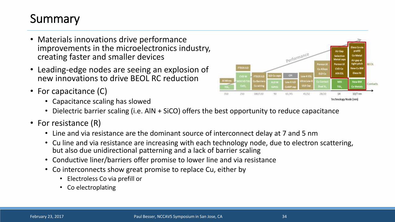
Summary
• Materials innovations drive performance improvements in the microelectronics industry, creating faster and smaller devices
• Leading-edge nodes are seeing an explosion of new innovations to drive BEOL RC reduction
• For capacitance (C) • Capacitance scaling has slowed • Dielectric barrier scaling (i.e. AlN + SiCO) offers the best opportunity to reduce capacitance
• For resistance (R) • Line and via resistance are the dominant source of interconnect delay at 7 and 5 nm • Cu line and via resistance are increasing with each technology node, due to electron scattering,
but also due unidirectional patterning and a lack of barrier scaling • Conductive liner/barriers offer promise to lower line and via resistance • Co interconnects show great promise to replace Cu, either by
• Electroless Co via prefill or • Co electroplating
February 23, 2017 Paul Besser, NCCAVS Symposium in San Jose, CA 34

Thank you
February 23, 2017 Paul Besser, NCCAVS Symposium in San Jose, CA 35


