AlD Vacuum Technologies GmbH - Bureau of Industry and Security

1
Before the Bureau of Industry and Security, Office of Technology Evaluation, U.S.
Department of Commerce
In the Matter of Executive Order 14017 of February 24, 2021 America’s Supply Chains
In Response to a Notice by Bureau of Industry and Security 86 Fed. Reg. 14308
Risks in the Semiconductor Manufacturing and Advanced Packaging Supply Chain
(March 15, 2021)
Submitted April 5, 2021
Written Comments from the Semiconductor Industry Association The Semiconductor Industry Association (SIA)1 welcomes the opportunity to provide written comments in the matter of Executive Order 14017 (“America’s Supply Chains”), Notice on Request for Public Comments on Risks in the Semiconductor Manufacturing and Advanced Packaging Supply Chain. The SIA agrees with the Biden Administration’s prioritization of the semiconductor for such review, given our technology is critical for U.S. economic growth, jobs, technology leadership, and U.S. national security.
1The Semiconductor Industry Association (SIA) is the voice of the semiconductor industry, one of America’s top export industries and a key driver of America’s economic strength, national security, and global competitiveness. Semiconductors – the tiny chips that enable modern technologies – power incredible products and services that have transformed our lives and our economy. The semiconductor industry directly employs nearly a quarter of a million workers in the United States, and U.S. semiconductor company sales totaled $208 billion in 2020. SIA represents 98% of the U.S. semiconductor industry by revenue and nearly two-thirds of non-U.S. chip firms. Through this coalition, SIA seeks to strengthen leadership of semiconductor manufacturing, design, and research by working with Congress, the Administration, and key industry stakeholders around the world to encourage policies that fuel innovation, propel business, and drive international competition. Learn more at www.semiconductors.org.

2
SIA’s main points in this submission and the accompanying report from SIA and the Boston Consulting Group are the following:
1. The global semiconductor supply chain provides enormous value in promoting innovation and reducing costs;
2. It would be unrealistically expensive and unproductive to attempt to replicate the global supply chain in any single country in an attempt to achieve self-sufficiency;
3. The global supply chain faces various vulnerabilities due to the concentration of certain sources of inputs in specific geographies; and
4. The U.S. should adopt smart policies to eliminate or reduce these vulnerabilities and enhance the U.S. economy, national security, and supply chain resilience.
I. Executive Summary Semiconductors have driven transformative advances in nearly every modern technology, from computers to mobile phones to the Internet itself, and they play a critical role in innovations in automobiles, medical devices, manufacturing, energy production, and other key areas of our economy and society. Chips also will underpin advances in the “must-win” technologies of the future, including artificial intelligence (AI), quantum computing, and advanced wireless networks (5G/6G). Continued U.S. leadership in semiconductor technology and an assured supply chain with a strong domestic base is critical to our future. U.S. companies have for decades led the world in producing these tiny chips that power modern technologies. Our country’s leadership in semiconductors is a big reason America has the world’s largest economy and most advanced technologies. This leadership is due to a range of factors, including very high levels of investment in research and development (R&D) by both the U.S. government in the early years of the industry, and by large manufacturers in the later years, including significant capital expenditure (capex) sustained by access to global markets and the ability to leverage a complex global supply chain and the best talent in the world. The U.S. industry, however, faces a range of challenges. The COVID-19 pandemic has upended the global economy and disrupted worldwide supply chains, causing significant near-term market uncertainty. The rising cost of innovation for semiconductor manufacturing and design, particularly at the leading edge for memory, logic, and advanced analog, continues to pose challenges. Additionally, while the U.S. remains the global leader in semiconductor design and R&D, the lion’s share of chip manufacturing is now occurring in Asia. This trend is supported by broad non-market incentives and policies by foreign nations who recognize manufacturing production as the critical key to microelectronics market dominance and military success. Finally, global geopolitical instability, is especially impacting trade policy, forcing the U.S. industry to consider how to remain competitive in a world of unforeseen uncertainty and policy constraints.

3
The U.S. semiconductor industry relies on its deep global supply chains and access to overseas markets, but there are significant risks for the United States. The global structure of the semiconductor supply chain, developed over the past three decades, has enabled the industry to deliver continual cost reductions and performance gains that ultimately has made possible the explosion in end user adoption of information technology and digital services. Semiconductors are highly complex products to design and manufacture. The need for deep technical know-how and scale has resulted in a highly specialized global value chain in which regions perform different roles according to their comparative advantages. All countries, particularly key U.S. allies, are interdependent in this integrated global value chain, relying on free trade to move materials, equipment, IP, and products around the world to the optimal location for performing each activity. However, some large foreign nations do not currently operate on an entirely free market and have significant restrictions and incentive targets for their own domestic production. This global structure creates enormous value for consumers, businesses, and governments who use semiconductors and products enabled by semiconductors. The global value chain helps drive innovation in semiconductor technology while reducing costs. In contrast, a hypothetical alternative with parallel, fully “self-sufficient” local semiconductor supply chains in each region to meet its current levels of semiconductor consumption would require at least $1 trillion in incremental upfront investment and would result in a 35 to 65 percent overall increase in semiconductor prices, and ultimately higher cost of electronic devices for end users.2 Clearly this hypothetical alternative to global value chains is a nonstarter for the semiconductor industry and the world, and the global semiconductor industry will continue to rely on the global value chain for the foreseeable future. However, China in its latest 14th 5 Year Plan is clearly attempting to buck these trends and generate a self-sufficient design and production capacity partially in response to technology and trade frictions but also due to their aim for “secure and controllable” indigenous supply chains. The process of researching, designing, and manufacturing semiconductors – including the specialized materials and equipment contributing to each step in the process – is so complex today that no one country or one company can do it alone. The U.S. has the opportunity to target and capture the next increment of semiconductor investments to help re-balance global production capacity into the U.S. and regions with better political and environmental stability. In the past few years, however, several factors have emerged that could put the successful continuation of this global model at risk. While geographic specialization has served the industry and its consumers well, it has also created potential vulnerabilities in the global value chain. For example,
1) There are more than 50 points across the value chain where one region holds more than 65% of the global market share.
2) About 75% of semiconductor manufacturing capacity, as well as many suppliers of key
materials (such as silicon wafers, photoresist and other specialty chemicals and sputtering targets), is concentrated in China and East Asia, a region significantly exposed to high seismic activity and geopolitical tensions and lack of fresh water and power.
2 These and other findings and background information about the global semiconductor supply chain in this submission can be found in the recently-released SIA and BCG report “Strengthening the Global Semiconductor Supply Chain in an Uncertain Era”, April 2020.

4
3) 100% of the world’s highly advanced (below 10 nanometers) logic semiconductor manufacturing capacity is currently located in South Korea (8%) and Taiwan (92%), due in no small part to healthy incentives and government support from these host nations.3
4) More than 60% of the world’s back-end semiconductor assembly, packaging and testing capacity is in China and Taiwan, and the U.S. lacks any large-scale, commercial state-of-the-art advanced packaging capability, including onshore outsourced assembly test (OSAT) facilities.
5) There are single points of failure in the value chain that could be disrupted by natural
disasters, infrastructure shutdowns, or geopolitical conflicts and may cause large-scale interruptions in the supply of essential chips.
6) In addition, geopolitical tensions may result in trade restrictions that impair access to
crucial providers of essential technology, unique raw materials, tools, and products that are clustered in certain countries. Such restrictions could also restrict access to important end markets, potentially resulting in a significant loss of scale and compromising the industry’s ability to sustain the current levels of R&D and capital intensity needed to maintain the current pace of innovation.
Industry participants and governments must join in efforts to address these vulnerabilities and to make the value chain more resilient, while also continuing to facilitate worldwide access to markets, technologies, capital, and talent. The U.S. government will need to use a combination of smart policies to mitigate these vulnerabilities, including targeted investments to fill high-risk gaps in their supply chains and collaboration with allies and partners globally to strengthen supply chains. For innovation to continue to thrive, the semiconductor industry needs targeted government policies and incentives that strengthen supply chain resiliency and expand market access while balancing the needs of national security. A key for the U.S. to build this supply chain resiliency will be to strengthen international alliances and partnerships. As this submission demonstrates, there is no one company or country that can achieve self-sufficiency in semiconductors. In addition to targeted domestic investments aimed at bolstering onshore capabilities, the United States must improve its alliances and partnerships with key countries and regions in the semiconductor industry globally to strengthen the resilience of the global semiconductor supply-chain. Many U.S. allies share similar concerns that the semiconductor supply chain is particularly vulnerable to geographic concentration in parts of East Asia, especially Taiwan. The U.S. government should work through existing multilateral and plurilateral forums (such as the WSC/GAMS, WTO, OECD, Wassenaar Arrangement, etc.) to coordinate key semiconductor supply-chain related issues such as supply-chain resilience, cyber security, joint R&D efforts, export controls, intellectual property protection, subsidies, and market access barriers. The immediate solution to these challenges should be focused – competitive government incentive programs must support domestic semiconductor research and achieve a more diversified geographical footprint by building additional semiconductor and unique raw material manufacturing capacity in the U.S. and expanding the production sites and domestic sources of supply for unique and critical materials. Beyond targeted incentives,
3 Logic semiconductors are highly sophisticated chips that serve as the main processor for electronic products such as PCs, smart phones, etc.

5
the government must guarantee a level global playing field, as well as strong protection of IP rights. The government must also take steps to further promote global trade and international collaboration on R&D and technology standards, particularly with allied countries. In parallel, policy makers should step up efforts to address the shortage of talent that threatens to constrain the industry’s ability to maintain its innovation pace through further investment in science and engineering education, as well as immigration policies that enable leading global semiconductor clusters to attract world-class talent. In addition, the government should establish a clear, stable, and targeted framework for targeted controls on semiconductors that avoid broad unilateral restrictions on technologies and vendors while establishing market incentives for more assured sources for our military and critical infrastructure needs. Such well-modulated policy interventions would preserve the benefits of scale and specialization in today’s global value chain structure, while addressing supply-chain risk with targeted investments to incent incremental capacity growth in the U.S. to domestic resiliency requirements and address worldwide market needs. This would ensure that the industry can extend its ability to deliver the continual improvements in semiconductor performance and cost that will make the promise of transformative technologies such as AI, 5G, IoT, and autonomous electric vehicles a reality in this decade, while providing domestic production capacity necessary for critical domestic applications. Critical to sustaining strong growth in domestic manufacturing is the ability to create market incentives for assured sources and supply chains for domestic and allied needs in, for example high-performance computing critical infrastructure, automotive, and 5-6G infrastructure investments. These assurance standards should enable open and free trade while taking supply assurance and stability, IP protections, and technology concentration into consideration.

6
II. Responses to Specific Questions from the FRN Below are additional comments and information on some of the specific topics posed in the Federal Register Notice.
(i) Critical and essential goods and materials underlying the semiconductor manufacturing and advanced packaging supply chain; Critical supply of upstream equipment, materials, chemicals, and gases The industry value chain involved in the creation and production of any semiconductor is extraordinarily complex and globalized. At a high level, semiconductor design and manufacturing consists of three broad stages, supported by a specialized ecosystem of goods, materials, equipment, and software design tools:
1. Semiconductor design Firms involved in design develop the nanometer-scale integrated circuits which perform the critical tasks that make electronic devices work, such as computing, storage, connectivity to networks, and power management. Design relies on highly advanced electronic design automation (EDA) software and reusable architectural building blocks (“IP cores”), and in some cases also outsourced chip design services provided by specialized technology suppliers.
2. Wafer fabrication (front-end manufacturing) Highly specialized semiconductor manufacturing facilities, typically called “fabs”, print the nanometer-scale integrated circuits from the chip design into silicon wafers utilizing photolithographic masks (photomasks) each imprinted with the designers IP. Each wafer contains multiple chips of the same design. The actual number of chips per wafer depends on the size of the specific chip and wafer size: it could vary between a hundred of the large, complex processors that power computers or smartphones, to hundreds of thousands for small chips intended to perform a simple function.
3. Assembly, packaging and testing (back-end manufacturing) This stage involves converting the silicon wafers produced by the fabs into finished chips that are ready to be assembled into electronic devices. Firms involved at this stage first test wafers to identify good chips, then slice silicon wafers into individual chips. Good chips or “dies” are then selected and packaged into protective frames and encased in a resin shell. Packaged chips are further rigorously tested before being shipped to electronic device manufacturers for subsequent assembly onto printed circuit boards that will be incorporated into computers, phones, and other devices.
A highly specialized upstream supply ecosystem Semiconductor design and manufacturing companies involved in these three stages of production activities rely heavily on an upstream ecosystem of specialized suppliers. At the design stage, electronic design automation (EDA) companies provide sophisticated software and services to support the design of semiconductors, including outsourced design of specialized application specific integrated circuits (ASICs). With billions of transistors in a single chip, state-of-the-art EDA tools are indispensable to design competitive modern

7
semiconductors. Core IP suppliers license reusable components designs – commonly called “IP blocks” or “IPs” – with a defined interface and functionality to design firms to incorporate into their chip layouts. These also include foundation physical IPs associated with each manufacturing process node, as well as many interface IPs. EDA and core IP vendors invest heavily in R&D – about 30 to 40% of their revenues – and accounted for approximately 4% of the value added of the industry in 2019. Semiconductor manufacturing uses more than 50 different types of sophisticated wafer processing and testing equipment provided by specialist vendors for each step in the fabrication process. These tools are necessary to imprint the design layers from the masks into planarized patterns of metal, dielectric, and dopants on the semiconductor wafers (Exhibit 8).
9 Copyri
ght
© 2
021 b
y B
ost
on C
onsu
ltin
g G
roup.
All
rig
hts
rese
rved.
EXHIBIT 8 | Semiconductor production involves more than 50 types of high-cost, sophisticated specialized equipment
1. Rapid thermal processingSources: Gartner
LithographyDeposition Assembly
equipment
Photoresist
processing
RTP1 &
oxidation
diffusion
Material
removal &
cleaning
Process
control(metrology
& inspection)
Doping
equipment
Manufacturing
automationTOTALOther
wafer
fabrication
equipment
Test &
related
equipment
64
6
12 1
12 2
16 1
3 26
3
BREAKDOWN OF MARKET SIZE OF SEMICONDUCTOR MANUFACTURING EQUIPMENT BY MAJOR FAMILIES, 2019 ($ BILLION)
FRONT END
BACK END
# EQUIPMENT
FAMILIES
12 4 6 1 12 4 2 2+ 3 5 50+16
Lithography tools represent one of the largest capital expenditures for fabrication players and determine how advanced of a chip a fab can produce. Advanced lithography equipment, specifically those that harness Extreme Ultra-Violet (EUV) technology are required to manufacture chips at 7 nanometers and below. EUV technology took two decades and billions of dollars in R&D to develop.4 A single EUV machine can cost $150 million and considerable operations and maintenance costs. Deposition and etch tools comprise a majority of semiconductor manufacturing process steps. The etch process removes selected areas from the surface of the wafer so that other materials may be deposited. The deposition processes create layers of dielectric (insulating) and metal (conducting) materials used to build a semiconductor device.
4 https://www.spiedigitallibrary.org/ebook/Download?fullDOI=10.1117%2F3.769214.ch2&SSO=1.

8
Metrology and inspection equipment is also critical for the management of the semiconductor manufacturing process. Because the process involves hundreds of steps over one to two months, if any defects occur early in the process, all the work undertaken in the subsequent time-consuming steps will be wasted. Strict metrology and inspection processes using specialized equipment are therefore established at critical points of the semiconductor manufacturing process to ensure that a certain yield can be confirmed and maintained. Modern fabs also have advanced automation and process control systems for direct equipment control, automated material transportation and real-time lot dispatching, with many of the newest facilities almost entirely automated. Semiconductor manufacturing equipment also incorporates many specialty subsystems and components with specific functionality, such as optical or vacuum subsystems, gas and fluid management, thermal management or wafer handling. These subsystems are provided by hundreds of specialized suppliers. Developing and fabricating such advanced, high-precision manufacturing equipment also requires large investments in R&D. Semiconductor manufacturing equipment companies typically invest 10 to 15% of their revenues in R&D. Overall semiconductor equipment manufacturers suppliers accounted for 9% of the R&D and 11% of the value added of the industry in 2019. Finally, firms involved in semiconductor manufacturing also rely on specialized suppliers of materials. Semiconductor manufacturing uses as many as 300 different inputs, many of which also require advanced technology to produce. For example, the polysilicon employed to make the silicon ingot that is subsequently sliced into wafers is required to have a purity level that is 1,000 times higher than the level required for solar energy panels, and is provided primarily by just four companies, with a combined global market share above 90%. Exhibit 9 shows the breakdown of the global sales of semiconductor manufacturing materials in 2019 across the key families used in front-end and back-end manufacturing.

9
10 Copyri
ght
© 2
021 b
y B
ost
on C
onsu
ltin
g G
roup.
All
rig
hts
rese
rved.
EXHIBIT 9 | Semiconductor production uses hundreds of unique materials and specialty chemicals
36%
12%13%
16%
7%
7%
7%
Gases
Silicon wafers
Photomask
CMP1 slurries and pads
Photoresist and
ancillary chemicals
Sputtering target
Wet chemicals
2%
Others
Breakdown of market size of semiconductor manufacturing materials, 2019 (% of $ Billion)
Front-end
materials
$33B
FRONT END (WAFER FABRICATION) BACK END (ASSEMBLY AND TEST)
15%
48%
6%
10%
15%
3% 3%Leadgrames
Die attach materials
Ceramic packages
Encapsulation resins
Others
Organic substrates
Bonding wire
Back-end
materials
$19B
1. Chemical-mechanichal planarizationSources: BCG analysis based on data from SEMI, IHS and HSBC
The main front-end manufacturing materials include:
• Polysilicon is a metallurgical grade silicon in ultra-refined purity levels, suitable for use in semiconductor wafer production.
• Silicon wafers. Polysilicon is melted, formed into single crystal ingots which are then sliced into wafers, cleaned, polished, and oxidized in preparation for circuit imprinting within fabrication facilities.
• Photomask is a plate covered with patterns used in the lithography process. The patterns consist of opaque and clear areas that prevent or allow light through.
• Photoresist is a special material that undergoes a chemical reaction upon exposure to light. Silicon wafers are covered with a photoresist layer, which is imprinted with the patterns contained in the photomask during the lithography process.
• Wet processing chemicals are used in the etching and cleaning steps of the semiconductor manufacturing process, and include solvents, acids, etchants, strippers and other products.
• Gases are used to protect wafers from atmospheric exposure. Other gases are used in the semiconductor manufacturing process as dopants, dry etchants, and in deposition processes.
• Chemical Mechanical Planarization (CMP) slurries are materials used for polishing the surface of the wafer after the film deposition step to provide a flat surface.
• Sputtering Targets are highly precise machined alloys used to deposit the metal needed to create the interconnects of the transistors on the wafer.

10
The following chart summarizes some of the key material inputs to the semiconductor manufacturing process:
Back-end materials include leadframes, organic substrates, ceramic packages, encapsulation resins, bonding wires and die-attach materials. They typically have relatively lower technical barriers to produce compared to the wafer fabrication materials described above. Production of these highly specialized materials is done in large plants, which also require high investments. Annual capital expenditure by the leading global suppliers of silicon wafers, photoresistors or gases typically ranges between 13 and 20% of their revenues. Overall, materials suppliers contributed 6% of the total capital expenditure and accounted for 5% of the value added of the industry in 2019. Intellectual property One of the most important components underlying the semiconductor manufacturing supply chain is intellectual property. In the semiconductor industry, companies invest billions in researching and developing to create the next best product. Development and qualification for production of a new process node often requires $1-10B dollars and large numbers of highly trained engineers and specialists depending on the device features and dimensions. Only a small group of firms have been able to deliver the investments and technology necessary for <7nm feature sizes. This semiconductor manufacturing process development requires its own research in areas such as process technology, manufacturing also leverages research and the resulting intellectual property developed in semiconductor manufacturing equipment, semiconductor designs, and more. As a result, it is critical that intellectual property across the semiconductor supply chain is protected. The continued success of our industry and continued American leadership in semiconductor design and manufacturing depends on a strong and balanced patent system and strong protections for trade secrets.

11
(ii) manufacturing and other capabilities necessary to produce semiconductors, including electronic design automation software and advanced integrated circuit packaging techniques and capabilities; Chip design Design activity is largely knowledge- and skill-intensive: it accounts for 65% of the total industry R&D and 50% of the value added. Indeed, firms focusing on semiconductor design typically invest 12 to 20% of their annual revenues in R&D. Development of modern complex chips, such as the “system-on-chip” (SoC) processors that power today’s smartphones, requires several years of effort by a large team of hundreds of engineers, sometimes leveraging external IP and design support services. Development costs have been rising rapidly as chips have become increasingly complex. The total development cost of a new state-of-the-art system-on-chip for a flagship smartphone, including the specialized blocks required to process audio, video or provide high-speed wireless connectivity, could well exceed $1 billion. Derivatives that reuse a significant portion of a prior design or new simpler chips that can be manufactured in mature nodes would cost just $20 million to $200 million to develop.
Wafer fabrication (front-end manufacturing) The fabrication process is intricate and requires highly specialized inputs and equipment to achieve the needed precision at miniature scale. Integrated circuits are built in cleanrooms, designed to maintain sterile conditions to prevent contamination by particles in the air that could alter the properties of the materials that form the electronic circuits. For comparison, the ambient outdoor air in a typical urban area contains 35,000,000 particles of 0.5 micron or bigger

12
in size for each cubic meter, while a semiconductor manufacturing cleanroom permits absolutely zero particles of that size.5 Depending on the specific product, there are 400 to 1,400 steps in the overall manufacturing process of semiconductor wafers. The average time to fabricate finished semiconductor wafers, known as the cycle time, is about 12 weeks, but it can take up to 14-20 weeks to complete for advanced processes. It utilizes hundreds of different inputs, including raw wafers, commodity chemicals, specialty chemicals, specialty sputtering targets, as well as many different types of processing and testing equipment and tools, across a number of stages (Exhibit 6). These steps are often repeated many hundreds of times, depending on the complexity of the desired set of electronic circuits.
7 Copyri
ght
© 2
021 b
y B
ost
on C
onsu
ltin
g G
roup.
All
rig
hts
rese
rved.
EXHIBIT 6 | Overview of the wafer fabrication process
Advances in manufacturing process technology are typically described by referring to “nodes”. The term “node” is meant to refer to the size in nanometers of the transistor gates in the electronic circuits, although over time it has lost its original meaning and has become an umbrella term to designate both smaller features and also different circuit architectures and manufacturing technologies. Generally, the smaller the node size, the more powerful the chip, as more transistors can be placed on an area of the same size. This is the principle behind “Moore’s Law”, a key observation and projection in the semiconductor industry that states that the number of transistors on a memory or logic chip doubles every 18 to 24 months. Moore’s
5 As geometries get smaller on chips, nanometer level contamination control is necessary for the leading-edge
technology. Amines, acids and organic contamination control require different sensing, monitoring and filtering technology to keep up with cleanroom environmental needs.

13
Law has underpinned the relentless pace of simultaneous improvement in performance and cost for processors since 1965. Today’s advanced processors found in smartphones, computers, gaming consoles and data center servers are manufactured on 5 to 10-nanometer nodes. Commercial high volume manufacturing (HVM) using 3-nanometer process technology is expected to begin in the Spring of 2022. Fewer firms are manufacturing semiconductors at the leading edge, because as time has progressed, leading-edge semiconductors have become more difficult and costly to produce. However more mature nodes, defined as 12nm and larger satisfy the remaining demand for semiconductors. Currently, the remaining firms manufacturing at the leading-edge process technology (defined as 10 nanometer and less) are from only three countries: Taiwan, Korea, and the United States.6
Table 1: number of global chip firms manufacturing at the leading edge, by year
6 Advanced memory semiconductor manufacturing is also measured in nanometer length nodes, though direct comparisons to logic nodes are difficult. Both advanced logic and memory semiconductors require high levels of R&D and capex intensity, and various end-use applications depend on both of these types of chips as well as a host of others such as discretes, analog, and optoelectronics, to fully function.

14
While logic and memory chips used for digital applications greatly benefit from the scaling in transistor size associated with smaller nodes, other types of semiconductors – particularly those in the DAO group (discrete, analog, and optoelectronics) described above – do not achieve the same degree of performance and cost benefits by migrating to ever smaller nodes, or simply use different types of circuits or architectures that would not work at more miniaturized scales. As a result, today wafer manufacturing still takes place across a wide range of nodes from the current “leading node” at 5-10 nanometers used for advanced logic and memory to the legacy nodes above 180 nanometers used for discrete, optoelectronics, sensors, and analog semiconductors. In fact, only 2% of the global capacity is currently on advanced nodes at 10 nanometers or below (Exhibit 17). And the vast majority of devices in use today rely upon
technologies at node sizes 12nm and above.
8 Copyri
ght
© 2
021 b
y B
ost
on C
onsu
ltin
g G
roup.
All
rig
hts
rese
rved.
EXHIBIT 7 | Global manufacturing capacity by node and semiconductor type
GLOBAL MANUFACTURING CAPACITY BY NODE AND SEMICONDUCTOR TYPE, 2019 (% of 8" equivalent wafers per month)
1. Discrete, analog and other (including optoelectronics and sensors) 2. Includes data centers and communication networksSources: BCG analysis based on SEMI data
<= 10 nm
5%
95%
14-22 nm
34%
>180 nm
19%
15%7%
60%62%
55-90 nm
9%
33%40%
28-45 nm
13%
110-180 nm
19%
76%68%
24%
5%
85%
24%
5%
39%
32%
29%
100%
Overall
% of total
DAO1
Logic
Memory
Front-end manufacturing is highly capital intensive due to the scale and complex equipment needed to produce semiconductors. A state-of-the-art semiconductor fab of standard capacity requires roughly $5 billion (for advanced analog fabs) to $20 billion (for advanced logic and memory fabs) of capital expenditure, including land, building, and equipment. This is significantly higher than, for example, the estimated cost of a next-generation aircraft carrier ($13 billion) or a new nuclear power plant ($4 billion to $8 billion).7 Capital expenditure of firms focusing on semiconductor manufacturing typically amounts to 30 to 40% of their annual revenues. As a result, wafer fabrication accounts for approximately 65% of the total industry capital expenditure and 25% of the value added. The top global locations for semiconductor wafer fabrication capacity share are Taiwan (22%), South Korea (21%), Japan (15%), and China (15%).
7 SIA and BCG report “Government Incentives and US Competitiveness in Semiconductor Manufacturing”, September 2020.

15
Assembly, packaging and testing (back-end manufacturing) The back-end stage of the supply chain still requires significant investments in specialized facilities. Firms specializing in assembly, packaging and testing typically invest over 15% of their annual revenues in facilities and equipment. Although it is relatively less capital-intensive and employs more labor than the front-end fabrication stage, new innovations in advanced packaging are changing this dynamic. Overall, this activity accounts for 13% of the total industry capital expenditure and contributed 6% of the total value added by the industry in 2019. It is concentrated primarily in Taiwan and mainland China, with new facilities also being built recently in Southeast Asia (Malaysia, Vietnam, and the Philippines).8
(iii) the availability of the key skill sets and personnel necessary to sustain a competitive U.S. semiconductor ecosystem, including the domestic education and manufacturing workforce skills needed for semiconductor manufacturing; the skills gaps therein, and any opportunities to meet future workforce needs; The U.S. semiconductor industry retains technological preeminence due to the knowledge, skills, training, and resources of the semiconductor workforce. Consequently, the highest priority change for the U.S. federal government should be to stimulate the supply of qualified workers for the semiconductor industry in the near term by swiftly reforming our high-skilled immigration system to allow STEM graduates of U.S. institutions to remain in and work in the U.S., and simultaneously to increase the total number of U.S. domestic STEM students who qualify to enter into all skill levels in the semiconductor field. In addition, any federal strategy should address inclusion of students from underrepresented populations.9
Attracting and retaining U.S. semiconductor talent
87 percent of semiconductor patents awarded to top U.S. universities had at least one foreign-born inventor. Between 2000 and 2010, the United States enjoyed a net influx of about 100,000 electrical engineering patent holders.10 The best-and-brightest students from around the world are attracted to our world-class universities, but once they have their diplomas, current U.S. immigration policy makes it almost impossible for these educated professionals to work, live, and contribute to the American economy. There is bipartisan support for reforming current green card policies for highly skilled immigrants, and strong government leadership is needed to make progress on this issue. The government should act swiftly to end per-country green card caps and exempt advanced STEM degree graduates of U.S. universities from existing green card caps.
From an immigration perspective, one way to increase the number of U.S. workers is to accelerate the permanent residency process for those that qualify for highly skilled immigrant visa categories (National Interest, Extraordinary Ability, Outstanding Researchers, etc.) through targeted immigrations reforms such as eliminating the per country limit on immigrant visas
8 Other semiconductor value chain activities further upstream from design, front-end fabrication, and back-end assembly, packaging, and test that contribute to value add for semiconductors include EDA & core IP, equipment & tools, and materials. 9 https://www.src.org/about/broadening-participation/. 10 The Chipmakers, CSET Issue Brief. May 2020.
16
coupled with recapturing unused immigrant visas from prior fiscal years. By speeding up the transition to permanent residency, highly skilled workers can switch from limited mobility work visas, such as the H-1B, and enter the unrestricted labor market as U.S. workers. In addition, the U.S. needs to immediately develop a strategy to bolster STEM education to improve the skills of the workforce and increase the pool of available talent. This strategy should include increased funding for K-12 STEM education and scholarships and apprenticeships.
In addition to semiconductor talent, the U.S. has been losing the talent pool to support the construction of cleanroom and production tool installation. High-skilled workers have been trained to work in the cleanroom environment installing utilities and production tools with concept of clean construction, but they have since moved to other sectors such as pharmaceutical and other general construction. It takes a long time, typically 5 or more years, to train such workers from apprentice to journeyman to handle many types of piping, interconnect and production tools. The current pool of this high paying labor is too small, and we will need support to get H2B visa for foreign workers at the peak of production and support tool installations. It will take some time to build the experienced technicians pool to support leading-edge production facilities.
Drastically increasing the pipeline of diverse and underrepresented minorities in U.S. STEM students interested in semiconductor fields
STEM education programs should be rigorously evaluated, and funding should be allocated to scale up successful models for broader implementation. Several government funded programs, and industry funded programs, have proven positive outcomes and are ripe for larger investments to drive them to scale. However, there are currently no effective mechanisms to raise the significant funding needed to drive programs to larger regional and eventually national scale. Therefore, the government should ensure funds critical for educating our future technical workforce are allocated for the short and long term through the appropriate legislation.
In addition, the broader STEM pipeline, including the U.S. semiconductor workforce, lacks sufficient diversity. Representation of women and underrepresented minorities in STEM, and especially in the physical sciences and engineering, has been persistently well below the demographics of the country and enrollment in institutions of higher education overall. Many SIA firms have undertaken targeted diversity initiatives to improve their workforce diversity profile to match or exceed diversity within the pool of available talent. Firms both small and large have shown that through targeted approaches that include focused mentorship, bias training in hiring, and workforce cultural changes, they can improve representation of women and underrepresented minorities within their workforce. Despite efforts of SIA member companies, however, the diversity in the STEM and semiconductor talent pools remains insufficient.
Leveraging federally funded R&D to develop the domestic semiconductor workforce
Finally, increased federal investment in semiconductor research is critical in addressing the future workforce in the industry. Government investment in semiconductor research provides the “pipeline” of highly educated talent that can drive innovation in the semiconductor industry for decades to come. Federally-funded projects provide learning opportunities and experience that firms cannot provide or fund on their own (e.g., Exascale, Quantum Computing, or Electronics Resurgence Initiative programs). Unfortunately, federal investment in research relevant to the semiconductor industry has been flat or declining in recent years. This decline in federal research investment is particularly harmful given that our global competitors are

17
drastically increasing their commitment to funding research, which will place U.S. leadership in the semiconductor industry at risk.
Manufacturing and technical workers
The establishment of a new major semiconductor fabrication site can exceed the infrastructure requirements and costs required for a new nuclear power plant. Construction and installation of semiconductor tools requires specialized and skilled labor to connect the tools to power, gas, water, cooling, and IT control systems. Currently, the cost of labor in the US is 1.5x that of our competitors and is often simply not available for large fabrication builds. Some semiconductor materials and components, such as quartzware and sputtering targets, require skilled machinists to fabricate the final product. U.S. suppliers of these materials are limited, and makers of semiconductor manufacturing equipment, report constraints in finding skilled, qualified machinists. Skilled workers in some of these fields (e.g., a skilled glass blower to work with hot work quartz or a skilled craftsman to machine a sputtering target) can take a year to train. Although overseas sources of these materials/components can be relied on to supply additional demand, any appreciable uptick in demand (i.e., a single major fab ramping) will cause supply-chain tightness, shortages and allocations.
(iv) risks or contingencies that may disrupt the semiconductor supply chain (including defense, intelligence, cyber, homeland security, health, climate, environmental, natural, market, economic, geopolitical, human-rights or forced labor risks): The global structure of the semiconductor supply chain, developed over the course of the past three decades, has served the industry well. Ultimately, it has enabled the explosion in innovation and end user adoption of information technology, which has benefited consumers and businesses immensely. However, in the last few years several new factors have emerged that could put the successful continuation of this global model at risk. Obviously, the COVID-19 global pandemic over the past year plus, has brought out into sharper relief vulnerabilities in global supply chains in general and in the semiconductor industry supply chain specifically, many of which will be described below.

18
Broadly speaking there are a number of types of risks that the semiconductor industry faces:
In fact, over the last three decades, the benefits of geographic specialization based on comparative advantage have resulted in the emergence of a more concentrated and interdependent global semiconductor supply chain. While not exhaustive, our analysis shows that there are more than 50 points across the overall supply chain where a single region accounts for 65% or more of the total global supply (Exhibit 19).

19
19 Copyri
ght
© 2
021 b
y B
ost
on C
onsu
ltin
g G
roup.
All
rig
hts
rese
rved.
EXHIBIT 19 | Multiple points of high geographical concentration across the current semiconductor value chain
1. For Design, EDA & Core IP, Equipment & Tools and Raw Materials: global share measured as % of revenues, based on company headquarter location. For Manufacturing (both Front End and Back End) measured as % of installed capacity, based on location of the facilitySources: BCG analysis with data from Gartner, SEMI, UBS; SPEEDA
FRONT END
Wafer fabrication
DESIGN BACK END
Assembly & Test
MANUFACTURING
VALUE CHAIN ACTIVITIES WHERE ONE SINGLE REGION ACCOUNTS FOR ~65% OR MORE OF GLOBAL SHARE1
EDA & CORE IP EQUIPMENT & TOOLS MATERIALS
23 equipment types,
i.e. doping, process control
12 equipment types,
i.e. photoresist processing
3 equipment types,
i.e. EUV lithography
EDA
IP (Arm architecture)
Advanced processors (CPU, GPU,
FPGA) and DSP
RFFE and cellular basebands
Data converter, switchers,
multiplexers and other analog
DRAM
Logic: advanced nodes
(< 10nm)
Logic: mature nodes
(>= 10nm)
Memory+ +
+ +
+ + Outsourced
Assembly and Test
(OSAT)
+
+
Select examples (not exhaustive):
Photoresist, photomask
Specialty gases (in aggregate)
US
China
Taiwan
South Korea
Japan
EU
UK
Silicon wafers
Packaging substrates
In many instances, there are no known alternatives for these materials, chemicals, and gases, and therefore assured supply of these materials is essential. The following is a partial list of essential inputs into the manufacturing process that may be subject to supply chain vulnerabilities:
• Process chemicals – The industry uses a range of process chemicals, including specialized fluorochemicals with unique performance attributes, in lithography, patterning, plasma etch, and other steps in the process. Many of these inputs have concentrated sources of production, such as in Japan.
• Wet chemicals – The wet chemicals supply-chain (HF, H2SO4, HCL, H2O2, H3PO4, NH4OH) runs extremely lean with such low profits that all chemical manufacturers within N. America have not committed to further expansion, for fear of losing money or they have exited the semiconductor industry. These materials continue to have supply-chain shortages virtually every year for U.S. chip fabs.11 It is critical that the remaining domestic suppliers are incentivized to maintain and expand production capacities to support domestic semiconductor production.
• Industrial gases – Semiconductor manufacturing requires the use of gases, including perfluorinated compounds, hydrofluorocarbons and noble gases such as helium, xenon, krypton, and neon and more common gases such as CO2. Some of the noble gases are sourced from countries of high geopolitical risk. For example, helium is primarily sourced from Qatar and Russia, and there is a high level of dependency on Ukraine for sources
11 H2O2, H2SO4 and NH4OH are high consumption materials that have to be delivered by trailer tanker trucks. It is not realistic to import these chemicals due to the high volume required. The quality of these bulk materials in particle and metallic contamination are poor compared to that in Asia due to lack of investment to improve production quality.

20
of xenon. Others such as PFCs and HFCs are essential to semiconductor manufacturing. There are no alternatives, but the future use of these gases may face potential restrictions due to global warming concerns.
• Metals/Materials – The industry uses key metals (e.g., titanium, tungsten, aluminum, copper) and rare earth materials. These metals are used in creating highly specialized sputtering targets that enable the deposition of metal onto wafers for the formation of transistors. For advanced node technologies continued and significant R&D and manufacturing investments and expansions are needed to support future growth and advancements.
• Commodity chemicals – Fabs also use commodity chemicals that may be produced by a wide range of suppliers. However, the semiconductor industry requires high purity chemicals (e.g., HCl, IPA, etc.) where there is a smaller group of qualified suppliers.
A number of the chemicals used by the semiconductor industry are byproducts of the production of other products. For example, helium is usually produced as a byproduct of natural gas, so the demand and market price for natural gas may determine if whether it is economic to extract helium from a well. Thus, supply-demand shifts and comparative production costs in different countries for commodities from which semiconductor chemicals or materials are a byproduct can create unanticipated risks to the semiconductor supply chain.
While geographic specialization has served the industry well, the observed high degree of geographic concentration in certain activities also creates two types of vulnerabilities:
• Single points of failure due to high geographic concentration of some activities that could result in large-scale supply interruptions
• Geopolitical tensions that may impair global access to suppliers or customers

21
Single points of failure that create risk of large-scale supply interruptions
The semiconductor manufacturing process is complex. Excessive geographic concentration in manufacturing exposes the industry to single points of failure which may be disrupted by natural disasters, infrastructure failures, cyberattacks or geopolitical frictions – from tariffs and export controls to even supply blockage resulting from broad embargoes or armed conflicts. Numerous examples of such disruptions, albeit contained in scale and duration to date, can be found in the last thirty years:
• The impact of the explosion of a Sumitomo Chemical factory in Japan in 1993 is often cited to illustrate the magnitude of this risk. It impacted 60% of the global supply of epoxy resin, and spot prices for DRAM memory chips in the U.S. market spiked from an average of $30/megabyte to around $80/megabyte.
• A strong earthquake in the center of Taiwan in September 1999 caused a six-day shutdown of the Hsinchu Science Park due to power outages. As a result, memory-chip prices tripled and shares of electronics companies around the world tanked, with IBM, Hewlett Packard, Intel, and Xerox, all part of the Fortune 100 at the time, losing 18 to 40% of their value in the month after the earthquake.
• In 2011 a major earthquake struck Japan, followed by a tsunami and nuclear power-plant melt down. 25% of the global production of silicon wafers and 75% of the global supply of hydrogen peroxide was affected by the disaster. Several fabs were shut down for several months.
• In 2019, geopolitical tensions between Japan and South Korea rose sharply. Japan imposed export controls on semiconductor materials to Korea, impacting approximately $7 billion in semiconductor exports per month.
• In December 2020, a power outage affected a memory fab located in Taiwan for just one hour, impacting 10% of global DRAM supply.
• Two fires at a package substrate plant in Taiwan in October 2020 and February 2021 aggravated the global capacity shortage for assembly, material, packaging and testing services, which was already experiencing difficulties to meet the surge in semiconductor demand in the last few months of 2020.
• Widespread power failures in Texas and a fire in a Renesas fab in Japan in early 2021 further exacerbated a short-term global chip supply shortage, especially for the automotive end-use market.
• Taiwan is currently experiencing a shortage in their freshwater reservoirs (less than 20%) and has to bring in fresh water necessary for semiconductor fabrication to deal with the shortage.
A high degree of geographic concentration of supply also exists in some semiconductor equipment as well as materials, such as silicon wafers, sputtering targets, photoresist, some chemicals such as packaging substrates, and specialty gases. While each specialty material

22
accounts for only a tiny portion of the industry’s total value added, semiconductors cannot be fabricated without them. While there is foreign availability in most cases, it is worth noting that in a situation where there is a short-term disruption, a chip maker cannot easily switch suppliers.
As an example, C4F6 is a critical process gas used to make 3D NAND memory and some advanced logic chips. It is essential for the etching process during chip fabrication, allowing etching to be completed 30% faster than the nearest alternative. Furthermore, once a manufacturing process is developed to use C4F6, it cannot be easily substituted. Identifying and qualifying alternative chemistries may take 10-15 years with no guarantee that a successful alternative will be found. Sales of C4F6 were approximately $250 million in 2019, with the top three suppliers located in Japan (40% of global supply), Russia (25%), and South Korea (23%). If any of these top three producers were severely disrupted, the loss of $60-100 million in C4F6 supplies, could lead to about $10 to $18 billion of lost revenue for NAND alone downstream in the semiconductor chain – almost 175 times higher than the direct impact. If such disruption in a portion of C4F6 supply were to become permanent, NAND production levels would potentially be constrained for 2-3 years until alternative locations could introduce new capacity ready for mass production.
Geopolitical tensions that may impair global access to suppliers or customers
While not exposing the industry to the risk of immediate halt of manufacturing activity leading to component shortages for electronic device makers, geographic concentration of the ownership of the leading global suppliers – measured in terms of company headquarters location as a

23
proxy for where the technology is actually developed -- also exists in other points of the semiconductor value supply chain (see Exhibit 17 above).
• In semiconductor manufacturing equipment, U.S. firms collectively account for more than 50% share of the global market in 5 of the major manufacturing process equipment categories (deposition tool, dry/wet etch and cleaning, doping equipment, process control, and testers). Likewise, Japan has over a 90% share of the photoresist processing market, vital equipment to the lithography process. In addition, ASML – a European company – has practically a 100% global market share in the EUV lithography machines essential to manufacture on advanced nodes below 7 nanometers.
• US-headquartered firms collectively account for more than 90% share in advanced logic products such as CPUs, GPUs or FPGAs that power PCs, data center servers, AI analytics and automotive ADAS systems – although manufacturing of these products is largely done in Asian foundries.
• Likewise, three US-based firms – of which one now has a European parent company – have a combined 85% share in EDA software tools essential to design semiconductors
• In the core IP layer, Arm – a company headquartered in the UK, but with R&D operations in multiple locations including the U.S. – licenses the architecture and processor core designs that currently run practically every smartphone and an increasing portion of the embedded computing systems used in IoT applications in Consumer Electronics, Industrial and Automotive.
Under normal market conditions this may not present immediate supply issues. In some cases potential substitutes may exist in other countries, and these activities are typically easier to scale than wafer manufacturing. However, they could also be subject to disruptions in scenarios of trade or geopolitical conflict that introduce restrictions to access to suppliers or technology originated in certain countries. By strengthening alliances with key countries, such as Japan and Korea, the United States industry can position itself to best deal with trade or geopolitical conflict while ensuring supply chain security. Overall, geopolitical tensions have been rising globally in the last 10 years: the index measuring global geopolitical risk is back at the levels of the Gulf War in 1990-1991. Ongoing geopolitical tensions in key semiconductor trade corridors in Asia and between the U.S. and China present a rising risk to the industry supply chain. US-China frictions Semiconductors occupy a prominent position in the ongoing tensions between the U.S. and China that have escalated significantly since 2018. While semiconductors have been largely excluded from tariffs that both countries enacted on a range of imports from the other side, in 2019 and 2020, the U.S. government has imposed a series of export controls that restrict access to semiconductors containing U.S. technology for Chinese entities that it regards as acting contrary to U.S. national security or foreign policy interests.

24
As of March 2021, some of these export controls encompass the entire semiconductor supply chain, including EDA and manufacturing equipment that incorporates technology developed in the US. Given that U.S. companies are currently the only viable suppliers of EDA and critical equipment such as doping or metrology (see Exhibit 17), these controls for now effectively block the impacted Chinese entities from sourcing semiconductors, even from non-US suppliers. These rules have encouraged China to develop and seek alternatives, and although it may take some time to do so, the trend towards reduction of dependence on U.S. semiconductor suppliers and indigenization of the supply chain is beginning to take shape. China accounts for approximately 24% of the global semiconductor demand measured in terms of consumption (“criteria C” in Exhibit 3), which makes it the second largest market in the world almost at par with the US. Its position as the world’s largest manufacturing hub for electronic devices – for both Chinese and foreign companies – also makes China the top destination for exports of finished chips. In addition, China is investing aggressively in semiconductor manufacturing: it accounted for 15% of the world’s total capacity in 2020 and is forecasted to build 40% of the incremental capacity that will be added globally in the next decade.12
Continuation of these bilateral tensions could have profound negative consequences for the semiconductor industry. Both U.S. semiconductor companies and unique raw material manufacturers, and also foreign vendors that rely on technology developed in the U.S., may be blocked from selling to at least some significant Chinese customers, if not to any Chinese company at all. This could lead to a significant reduction in revenue for leading U.S. semiconductor companies across the supply chain as well as global non-US companies with a
12 SIA and BCG report “Government Incentives and US Competitiveness in Semiconductor Manufacturing”, September 2020, pp. 9-10, and 22. It should be noted not all current capacity in China is owned by Chinese companies.

25
significant R&D footprint in the US, compromising their ability to sustain their current investment levels in R&D and therefore slowing the pace of innovation across the industry. Perpetuation of the conflict may also trigger retaliation from China in areas that could directly or indirectly impact the semiconductor supply chain, such as rare earth materials and ten other critical inputs such as germanium, lithium or tungsten. Rare earths are a set of 17 metallic elements with electronic and magnetic properties needed in electronic products. Although these materials account for only a small portion of overall production costs, they are the building blocks of key components in cars, computers, and many other high-value products—and they are an often-overlooked vulnerability in global supply chains. Our analysis indicates that China leads in the extraction of 9 of the 17 critical raw-material inputs and in the refining of 14 of them. As rare earths are traded in commodity markets, restrictions on exports from China would be felt by the entire supply chain and could disrupt the global production of electronic devices and therefore depress demand for semiconductors. Finally, the US-China frictions are also fueling a desire to develop self-sufficiency in semiconductors. For China, this is mainly an amplification and acceleration of its longstanding efforts to develop a strong domestic semiconductor sector that gained further urgency with the “Made in China 2025” plan introduced in 2015. In the case of the US, the escalating strategic competition with China has recently exposed the risks associated with the high concentration of semiconductor manufacturing capacity in East Asia (and Taiwan in particular), sparking some public debates about the desirability of self-sufficiency in semiconductor manufacturing, too. In other areas of the world such as Europe, Japan and South Korea, the central position of semiconductors in the US-China conflict together with the impact of the recent widespread semiconductor shortage on the automotive industry, has brought attention to the critical importance of semiconductors for the economy. Furthermore, their own companies with global leading positions in some segments of the semiconductor industry have found themselves restricted from selling to Chinese entities by U.S. export controls due to their reliance on US-developed technology further upstream or downstream in the value chain. These firms in allied countries play a key role in the supply chain, augmenting and amplifying product supply and technology development. The U.S. semiconductor supply chain is more secure with the partnership of a diverse global network of strong firms in allied countries. It is preferable that these companies are able to continue their roles, rather than enabling companies based in non-allied countries to fill the space with their own technology, thereby hurting both U.S. companies and those of allies. Continued restrictions on these firms in allied countries could create a negative spiral—reduced growth, revenue and profits leading to smaller scale investments in production equipment and research and development—which would negatively impact U.S. customers and suppliers, the semiconductor industry, and the U.S. economy overall. Geographic Specialization In fabrication, which is extremely capital intensive, the availability of attractive investment conditions – particularly government incentives – and access to robust infrastructure (power and water supply, transportation and logistics) and a skilled manufacturing workforce at competitive rates have traditionally been the key success factors. Government incentives may account for up to 30-40% of the 10-year total cost of ownership (TCO) of a new state-of-the-art fab, which is estimated to amount to $10-15 billion for an advanced analog fab and $30-40 billion for advanced logic or memory.

26
The top global locations for semiconductor wafer fabrication capacity share are Taiwan (22%), South Korea (21%), Japan (15%), and China (15%). Combined these countries account for about 75% of the world’s total semiconductor manufacturing capacity – including all the leading-edge capacity at 7 nanometers and below currently in operation – and under current market conditions its share is expected to continue rising over the next decade (Exhibit 2). According to our analysis summarized in Exhibit 16, the TCO of a new fab located in the U.S. is approximately 25-50% higher than in Asia, and 40-70% of that difference is attributable directly to government incentives, which are currently much lower in the U.S. than in alternative locations.
17 Copyri
ght
© 2
021 b
y B
ost
on C
onsu
ltin
g G
roup.
All
rig
hts
rese
rved.
EXHIBIT 16 | Manufacturing economics are significantly more favorable in Asia, with government incentives driving most of the cost advantage
100
78
63
+29%
+23%
ESTIMATED 10-YEAR TOTAL COST OF OWNERSHIP (TCO1) OF REFERENCE FABS BY LOCATION (US INDEXED TO 100)
Advanced Logic
100
79
66
+27%
+20%
Advanced Memory Advanced Analog
1. TCO includes capital expenditure (upfront land, construction and equipment) + 10 years of operating expenses (labor, utilities, materials, taxes) 2. Refers to Taiwan and South Korea for logic, South Korea and Singapore for memory 3. With technology sharing agreements that give access to additional incentives such as equipment lease back with advantageous terms Source: BCG analysis
100
68
+47%n.a.
US
China3
Other Asia
location2
70%
12%
16%2%Government
incentives
Labor
Utilities
Construction 57%24%
16%3%
44%
36%
12%
7%
What drives the higher TCO of US-based babs
In particular, Taiwan has been investing in the development of its domestic semiconductor manufacturing industry since 1974, when the government selected semiconductors as a key focus industry to expand the economy beyond agriculture. Policies pursued by the government included both direct support in the form of setting up R&D labs and industrial parks and providing incentives for the construction of new fabs such as generous tax-credits that could cover as much as 35% of their capital expenses and 13% of their equipment purchases, as well as indirect incentives such as reform of the financial sector and capital markets to facilitate access to funding. While several of the incentive programs were reduced after 2009-2010, we estimate that Taiwan still provides incentives for new fabs worth 25-30% of their overall total cost of ownership over a 10-year period. This is in line with other Asian locations such as South Korea and Singapore, but currently well below mainland China. Further, these incentives are being expanded to include key unique raw material suppliers to support the full ecosystem needed in semiconductor manufacturing. In contrast, the incentives to new fab construction
27
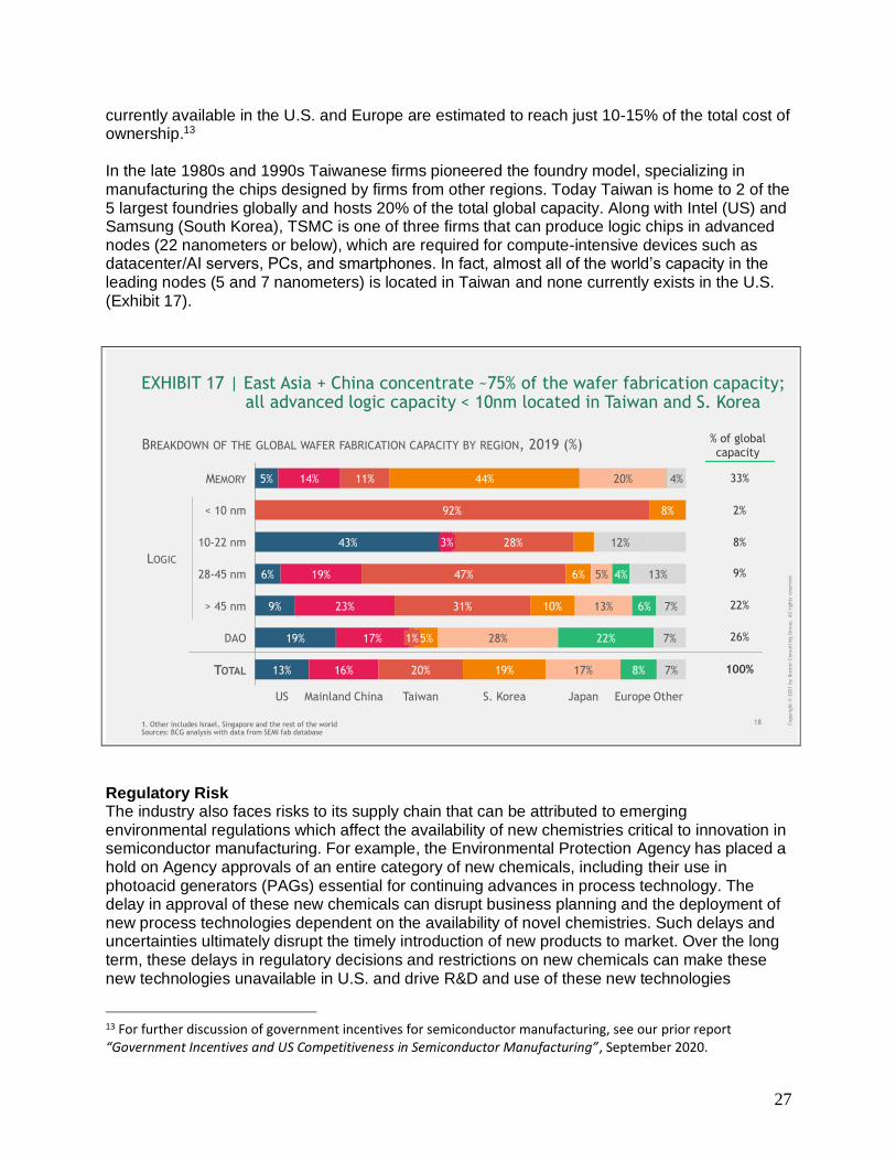
currently available in the U.S. and Europe are estimated to reach just 10-15% of the total cost of ownership.13 In the late 1980s and 1990s Taiwanese firms pioneered the foundry model, specializing in manufacturing the chips designed by firms from other regions. Today Taiwan is home to 2 of the 5 largest foundries globally and hosts 20% of the total global capacity. Along with Intel (US) and Samsung (South Korea), TSMC is one of three firms that can produce logic chips in advanced nodes (22 nanometers or below), which are required for compute-intensive devices such as datacenter/AI servers, PCs, and smartphones. In fact, almost all of the world’s capacity in the leading nodes (5 and 7 nanometers) is located in Taiwan and none currently exists in the U.S. (Exhibit 17).
18 Copyri
ght
© 2
021 b
y B
ost
on C
onsu
ltin
g G
roup.
All
rig
hts
rese
rved.
EXHIBIT 17 | East Asia + China concentrate ~75% of the wafer fabrication capacity; all advanced logic capacity < 10nm located in Taiwan and S. Korea
BREAKDOWN OF THE GLOBAL WAFER FABRICATION CAPACITY BY REGION, 2019 (%)
5%
43%
6%
9%
19%
13%
14%
19%
23%
17%
16%
11%
92%
28%
47%
31%
20%
44%
8%
6%
10%
5%
19%
20%
5%
13%
28%
17%
12%
4%
6%
22%
8%
4%
13%
7%
7%
7%
10-22 nm
Europe
< 10 nm
MEMORY
28-45 nm
> 45 nm
DAO 1%
TOTAL
OtherJapanS. KoreaTaiwanMainland ChinaUS
3%
LOGIC
1. Other includes Israel, Singapore and the rest of the worldSources: BCG analysis with data from SEMI fab database
% of global
capacity
33%
2%
8%
9%
22%
26%
100%
Regulatory Risk The industry also faces risks to its supply chain that can be attributed to emerging environmental regulations which affect the availability of new chemistries critical to innovation in semiconductor manufacturing. For example, the Environmental Protection Agency has placed a hold on Agency approvals of an entire category of new chemicals, including their use in photoacid generators (PAGs) essential for continuing advances in process technology. The delay in approval of these new chemicals can disrupt business planning and the deployment of new process technologies dependent on the availability of novel chemistries. Such delays and uncertainties ultimately disrupt the timely introduction of new products to market. Over the long term, these delays in regulatory decisions and restrictions on new chemicals can make these new technologies unavailable in U.S. and drive R&D and use of these new technologies
13 For further discussion of government incentives for semiconductor manufacturing, see our prior report “Government Incentives and US Competitiveness in Semiconductor Manufacturing”, September 2020.

28
offshore. Similarly, in recent years, there has been an increase in regulatory restrictions on the chemical composition of components embedded in complex “articles” (i.e., finished goods), including semiconductor manufacturing equipment. These new requirements can impose barriers on the introduction, movement, and maintenance of these products at fabs. The semiconductor industry will continue to work with EPA and other regulatory bodies to ensure the safe use of these chemicals and the development of appropriate regulations to address any risks posed by the industry’s use of these substances
a. Risks posed by reliance on digital products that may be vulnerable to failures or exploitation; The semiconductor industry supplies secure chips to the most sensitive and advanced facilities in both the public and private sector – such as weapons systems, banks, and telecommunications infrastructure. Customers demand that chips have supply chains that are verified and protected, and industry participants compete to provide new types of security functions and features, including supply chain verification. Further, semiconductor companies make a range of products for use across a wide variety of applications – from data centers to tablets, smartphones, and more. For example, with regards to logic chips, within any given chip product “family” there can be dozens of different types with unique features and capabilities. All depend on uniquely tailored operating code – known as microcode – that translates what computer software is designed to do into digital instructions that can be implemented on the microchips inside. For example, a smartphone app utilizes a semiconductor to convert physical swipes and taps into the movement of electrons in microchips that will, for example, result in a purchase order at an online store or money transfer request with your bank requires the complex interplay between software, microcode, and the physical chips. When a hardware vulnerability is discovered, semiconductor companies work with companies across the supply chain to understand that whole system – from the silicon chip to the microcode all the way up to the software. In accordance with the usual protocol established under voluntary industry standards and in the best interest of consumers and businesses, cybersecurity researchers who find hardware vulnerabilities often coordinate with semiconductor companies that make affected components on a timeframe for disclosing that vulnerability to the public. The existing standards and practices, known as coordinated vulnerability disclosure, say that unless people are known to be actively exploiting a vulnerability, it should not be disclosed publicly until a patch is ready to be deployed. The goal is to protect systems from attack, not necessarily speedy disclosure for its own sake. For particularly complicated vulnerabilities, such as those discovered in hardware, longer timeframes should be considered. Rigidly applying existing standard software public disclosure deadlines to semiconductor vulnerabilities, without consideration for the unique technologies of the semiconductor industry, can ultimately put users at risk by limiting the opportunity for the most effective mitigations to be developed and deployed before public disclosure of a vulnerability occurs. To mitigate overall risk to a rapidly advancing ecosystem, the federal government should fund pre-competitive, high-risk, high-reward research into security in the semiconductor field, as

29
recommended by the Decadal Plan for Semiconductor Research.14 For instance, new threat vectors through the emergence of quantum computing will create vulnerabilities in current cryptographic methods. Thus, encryption standards resistant to quantum attack must be developed, with consideration given to the impact of these standards on system performance. Consequently, increased federal funding for research in a number of areas, including research to advance the design and manufacture of trusted and secure hardware, is critical. Federal funding for cybersecurity researchers should be closely coordinated with the semiconductor industry to evaluate risks and mitigations.
b. risks resulting from lack of or failure to develop domestic manufacturing capabilities, including emerging capabilities; The largest risk to the U.S. is potential loss of access to viable semiconductor manufacturing and packaging if China or Taiwan are unwilling or unable to meet production demands. Additional risks include the inability to serve our critical infrastructure and defense needs with
assured parts and supply chain.15 Front-end fabrication: Unfortunately, the share of US domestic semiconductor manufacturing has declined to 12%, while Asia’s share has risen to over 70%. The National Security Commission on AI (NSCAI) stated that the dependency of the U.S. on semiconductor imports “creates a strategic vulnerability for both its economy and military to adverse foreign government action, natural disaster, and other events that can disrupt the supply chains for electronics.”16 Given the significant concentration of semiconductor and unique raw material manufacturing in some locations, a drought or a power outage could result in anything from consumers not being able to purchase their electronic devices to medical device manufacturers not being able to produce critical technologies such as ventilators. The Department of Defense, in its annual industrial capabilities report to Congress, stated that the threat posed by a dependence on foreign sources for semiconductor products and unique raw materials “will become more pronounced as emergent technology sectors, such as Internet of Things (IoT) and AI, require commodity quantities of advanced semiconductor components.”17 Building a diverse semiconductor manufacturing ecosystem is critical to ensuring that the US has access to all of the electronic devices that power the economy and grow national security Advanced semiconductor packaging and test: Currently the lack of onshore at-scale advanced semiconductor packaging is a significant supply-chain vulnerability for the United States. While it is relatively lower-value add and the last stage of semiconductor production, it is increasing in strategic importance given more sophisticated packaging techniques are required to boost chip-performance. While semiconductor packaging is comparatively more labor intensive than other stages of chip production, this new increase in technology complexity has begun to shift this dynamic. Today, mainland China and Taiwan account for more than 60% of the world’s assembly, packaging and testing capacity. Recently OSAT firms have also started to diversify
14 file:///C:/Users/marya/Downloads/decadal-plan-full-report%20(5).pdf 15 However, leading edge semiconductor technology has long been dual use in character and developed by the commercial semiconductor industry rather than the defense industry. Indeed, defense applications of leading-edge semiconductor technology represent only a small fraction of the overall use of such technology. 16 https://www.nscai.gov/wp-content/uploads/2021/03/Full-Report-Digital-1.pdf. 17 https://www.businessdefense.gov/Portals/51/USA002573-20%20ICR_2020_Web.pdf?ver=o3D76uGwxcg0n0Yxvd5k-Q%3d%3d

30
their own global footprint, building new capacity in other locations with low labor costs such as Malaysia. In addition, the Department of Defense’s State-of-the-art (SOTA) Heterogeneous Integrated Packaging (SHIP) is a new program aimed at bringing some capability on shore to meet national security needs. However, the U.S. lacks any large-scale, commercial state-of-the art advanced packaging capability, including onshore OSAT facilities. Additionally, technological leadership and research and development tends to follow the production capabilities. Currently, the USG investments in R&D for next-generation microelectronics don’t have strong transition pathways to domestic production and instead often leverage subsidized wafer and foundry access provided by foreign nations. U.S. R&D investments in semiconductors are also not focused on enabling production leadership and face challenges in the transition to domestic ecosystems as compared to European and Asian R&D models and public-private partnerships (such as IMEC and CEA-LETI). Additionally, technological and leadership and the research and development tends to follow the production capabilities. Currently, the USG investments in R&D for next-generation microelectronics don’t have strong transition pathways to domestic production and instead often leverage subsidized wafer and foundry access provided by foreign nations. U.S. R&D investments in semiconductors are also not focused on enabling production leadership and face challenges in the transition to domestic ecosystems as compared to European and Asian R&D models and public-private partnerships (such as IMEC and CEA-LETI). The CHIPS for America Act authorizes the establishment of a National Semiconductor Technology Center (NSTC) to address these risks by creating a new leading, U.S.-based research capability for the semiconductor industry that does not exist anywhere in the globe due to the high cost and complexity of semiconductor R&D infrastructure. The research agenda proposed for the NSTC would allow public, private, and university partners to develop and prototype experimental semiconductor technologies. By providing researchers access to a consortia-run institution with the most advanced semiconductor research infrastructure in the world, the NSTC provides the opportunity for U.S. innovation to leapfrog global competition for leadership in a wide swath of technologies. Furthermore, by establishing an NSTC in the United States, the U.S. semiconductor industry and the U.S. industrial base will attract, retain, and train a new generation of the most advanced semiconductor technologists in the globe. Another key part of ensuring a strong domestic manufacturing base is ensuring a strong semiconductor design base that can use onshore manufacturing facilities. While the U.S. has traditionally been a leader in semiconductor design, that position is being challenged by competitors who are investing billions to grow their indigenous industry. According to one estimate by the Boston Consulting Group, semiconductor products worth 61% of global demand have at least one non-US company with a global market share of 10% or more, representing potential alternatives to US suppliers.18 Even in segments where the US holds greater than 90% of market share, many global customers are increasingly designing their own custom chips, known as application-specific integrated circuits (ASICs), for use in their own devices. A loss of a domestic semiconductor design base could threaten the entire semiconductor ecosystem and result in the US becoming reliant on foreign-developed semiconductors.
18 https://image-src.bcg.com/Images/BCG-How-Restricting-Trade-with-China-Could-End-US-Semiconductor-Mar-2020_tcm9-240526.pdf.

31
(v) the resilience and capacity of the semiconductor supply chain to support national and economic security and emergency preparedness, including:
a. Manufacturing or other needed capacities (including ability to modernize to meet future needs); Long-term global semiconductor demand will continue to increase over the next 10 years, and more of the demand will continue to shift to strategically important industries to the U.S.
Unfortunately, the trajectory of where semiconductor capacity to meet this domestic demand will be added is decreasing in the U.S. and increasing abroad. It is projected the U.S. will only be able to produce 10 percent of global semiconductor front-end fab capacity by 2030, down from 12 percent in 2020. Significantly, the country with the largest share of fab capacity by 2030 is estimated to be China.

32
Compared to other strategic industries to the U.S., 12 percent front-end fabrication capacity within its borders is relatively low and represents a vulnerability for the U.S. In addition, the U.S. currently has less than 5 percent of back-end assembly, test, and packaging capacity in the U.S.

33
Clearly, the U.S. will have future need for strategic technologies powered by semiconductors over the next 10 years. Presently, the U.S. currently lacks the domestic capabilities to meet those needs, and this gap is estimated to only widen, given current trends. For example, the U.S. military needs access to leading-edge semiconductors that our adversaries lack. Yet in an increasingly globalized semiconductor supply chain, the cybersecurity of the U.S. semiconductors industry is increasingly vulnerable to disruption from malware and other production defects. But despite the increasing cyber vulnerabilities, the most concerning is the continued offshoring of semiconductors production, research & development (R&D) and intellectual property (IP) to potential adversaries. Loss of American control of this vital component and its attendant supply chain raises the risks of compromise of one of our most important technologies. This national security threat demands close coordination between government and industry to address it effectively. According to TECHCET, an advisory services firm focused on process materials supply-chains, electronic materials business, and materials market analysis for the semiconductor, display, solar/PV, and LED industries, there are several needed capacities in material suppliers for the industry, including the following:
• UHP (ultra-high purity) IPA is currently being sourced from Taiwan for U.S. fabs. U.S. suppliers have not wanted to invest the money to build a supply chain that will support leading-edge quality IPA. It is our understanding that the challenge lies in both the starting material, i.e. that which comes from Exxon, as well as the lack of purification capability.
• There are only the following wafer manufacturing sites in the U.S., Shin-Etsu Handotai, Sumco, Siltronics and GlobalWafers (ex-MEMC, Globitech). The 300mm production supply in the U.S. is not sufficient to support all domestic needs and some portion of wafers is being shipped from Japan (SEH) and likely some from Taiwan (Global Wafers). If TSMC, Samsung, and Intel are expanding 300mm fab production then reliance on imported 300mm wafers will increase unless wafer makers invest and expand their capacity in the U.S. (The former MEMC, now GlobalWafers, plant in Missouri, currently only produce SOI wafers; their ingot and wafering had been shutdown.)
• There is only one WF6 manufacturing site in the U.S. owned by Japanese company. This site has no expansion capability and would need high investment to build additional plant capacity.
Additionally, there is a looming capacity and capability constraint for radiation-hardened chips, which are required for applications in space. This issue was identified in the 2017 Presidential Determination. Without improvements and investments in radiation test and qualification facilities projects – specifically proton and heavy ion testing- the U.S. is at risk of significant under capacity for testing critical defense components.

34
b. gaps in manufacturing capabilities, including nonexistent, threatened, or single-point-of-failure capabilities, or single or dual suppliers; Manufacturing is clearly a major point of concern for the resilience of the U.S. semiconductor supply chain. The top global locations for semiconductor wafer fabrication capacity share are Taiwan (22%), South Korea (21%), Japan (15%), and China (15%). Combined the share of these countries currently account for almost 75% of the global installed capacity. This region is significantly exposed to high seismic activity and geopolitical tensions. The number is even higher for advanced technologies: currently 100% of the global capacity in the leading 7- and 5-nanometer nodes is currently in East Asia. In particular, as shown before in Exhibit 17 as well as below in Case Study 1, Taiwan has 40% of the world’s logic chip production capacity and leads in the most advanced nodes at 10 nanometers or below that are required to manufacture chips such as application processors, CPUs, GPUs and FPGAs for smartphones, PCs, data center servers, and autonomous vehicles. In an extreme hypothetical scenario of complete disruption for one year, Taiwanese foundries would lose their current cumulative $42 billion in revenues, but that could also cause a $490 billion drop in revenue, or 12 times more negative impact, for electronic device makers across different application markets19. The global electronics supply chain would come to a halt, creating significant global economic disruptions. If such hypothetical complete disruption were to be become permanent, it could take a minimum of three years and $350 billion of investment in what would be an unprecedented effort to build enough capacity in the rest of the world to replace the Taiwanese foundries.
Case Study 1
19 Based on the estimated share of device applications that are supplied by chips produced by Taiwanese fabs, including PC/laptop/tablet, servers, smartphone, automotive electronics, and industrial cameras. Note, the Taiwan foundry revenue figure of $42 billion is from 2019. Total Taiwan foundry revenue for 2020 is likely between $55-65 billion.

35
According to TECHCET, most silicon wafers used in semiconductors are manufactured in Asia. In addition, HCl(g) has been single source in North America for several years and the existing manufacturer is existing the business, although a new manufacturer is now coming online. This type of gas is caustic and therefore difficult and expensive to import. Some gaps in the capacity to produce key manufacturing inputs are the result of governmental action. For example, fabrication requires the use of PAGs. When EPA entered into a consent order with the industry’s chemical suppliers that allows for the import of PAGs, the Agency did not allow for the domestic manufacture of these critical inputs.
c. location of key manufacturing and production assets, and risks posed by these assets' physical location; See section iv.
d. exclusive or dominant supply of critical or essential goods and materials by or through nations that are, or may become, unfriendly or unstable; As stated in section (i), the semiconductor manufacturing process uses many chemicals, gases, and materials that are sources from a limited number of sources overseas, including from areas vulnerable to geopolitical disruption or prone to natural disasters. One example of an essential input to the manufacturing process subject to potential supply vulnerability is helium. The U.S. has considerable reserves of helium, but under the Helium Stewardship Act of 2013 (P.L. 113-40), the federal role in the sale of helium is expected to end later in 2021. As a result, helium is increasingly sourced from Russia, Qatar, and other potentially vulnerable geographies. The chart below shows the relative decline in the U.S. production of helium relative to the rest of the world.

36
Other materials are also sourced from countries/regions of potential vulnerability, according to TECHCET, including the following:
• Rare Earths – Rare earths used in memory, logic, and analog are largely sourced in China, and the primary rare earths of concern include lanthanum, cerium and scandium. Lanthanum is used in the fabrication of logic devices of 14nm and below technology. Cerium is consumed to produced ceria slurry critical for advanced semiconductor production. Scandium is used in an aluminum-scandium alloy piezoelectric film critical for RF filters and other sensors.
• Fluorspar – China is the source of 60% or more of the fluorspar used in the semiconductor industry to make fluorine containing products include CF gases, NF3, HF, WF6, SF6. Many U.S. facilities source this material from Mexico, but most facilities located in Asia are dependent on China for sourcing.
• Tungsten – 80% of the world's tungsten mineral (APT, ammonium paratungstate) come from China. APT is used to make WF6 and W sputter targets. WF6 is used for the majority of all semiconductor devices. China represents about 80% of the mining production, with 95% of supply controlled by one company. There are reportedly new mining sources in Vietnam and possibly in South Korea.
• Ultra-high purity IPA – Most of this material is sourced from Taiwan, which is subject to extreme weather conditions and geopolitical risks
• The Platinum Group Metals (Palladium, Platinum, Ruthenium, Iridium, Rhodium) – This group of metals are sources largely in South Africa. According to TECHCET, these mines are apparently facing closure in the next 15 years or so, and new mines in Russia and the U.S. are expected to come online for Palladium and Platinum.

37
o Palladium – 45% to 50% of global supply is sourced from Russa. This metal is used to form electrodes, and plating/coating for lead frames and bonding wire.
o Platinum – 70% or more sourced from South Africa and is used for electrodes and silicide contacts.
o Ruthenium – used in applications in metal interconnect and electrode (for sensors, MRAM) applications, and over 90% is mined from South African sources. Currently recycle/recovery is critical in maintaining supply/demand balance.
Another area of potential concern is personal protective equipment (PPE), which is largely sourced in China. PPE is critical to semiconductor manufacturing due to the need to conduct operations under highly controlled conditions. Members of TECHCET have indicated that PPE from China, such as gloves, are in short supply. Also, see section iv.
e. availability of substitutes or alternative sources for critical or essential goods and materials; As noted earlier in section iv, semiconductor manufacturing requires the use of specialized equipment as well as materials like chemicals and gases that possess unique chemical and physical attributes. While there is suitable foreign availability in many cases, in some instances, there are no alternatives that satisfy the performance and functional characteristics required in advanced processes. High end substrate material for semiconductors represent an important example. These materials are primarily produced in Japan and Taiwan, which carry certain geopolitical, environmental, and other risks. For example, two fires at a package substrate plant in Taiwan in October 2020 and February 2021 aggravated the global capacity shortage for assembly, material, packaging, and testing services, which was already experiencing difficulties to meet the surge in semiconductor demand in the last few months of 2020. U.S. policy could explore potential incentives for increasing the volume and availability of domestically produced high end substrate.
f. need for research and development capacity to sustain leadership in the development of goods and materials critical or essential to semiconductor manufacturing; The U.S. semiconductor industry invests approximately one-fifth of its annual revenue into research and development, a higher share than almost any other industry, amounting to nearly $40 billion in 2019.

38
Federal investments in R&D, in contrast, have failed to keep pace with the rising costs of developing new technology, and global competitors, including China, are investing heavily to challenge U.S. leadership. Of these global competitors, the Information Technology and Innovation Foundation, notes that Chinese government has increased their R&D funding by 330 percent from $23 billion to $98 billion, while U.S. government R&D grew by just 2 percent from $121 billion to $124 billion from 2003-2017.
U.S. Government investment in R&D has been steadily declining in comparison to key competitors.

39
While there is no available data for the semiconductor industry, basic research typically accounts for 10-20% of the overall R&D investment in most leading countries. For example, in the United States it has remained stable over time at 16-19% of the total R&D. Basic research is performed by a global network of scientists from private corporations, universities, government-sponsored national labs and other independent research institutions that collaborate in joint research efforts.
In particular, governments have a very significant role in advancing basic research. A prior study of federal R&D by the Semiconductor Industry Association (SIA) identified 8 major semiconductor technology breakthroughs that emerged out of government-sponsored research programs. For example, the gallium arsenide (GaAs) transistors that enable smartphones to establish a wireless communication link to cellular towers was created in the Microwave and Millimeter Wave Integrated Circuit (MIMIC) program of the Department of Defense in the late 1980s. EUV manufacturing technology, which enables lasers to create ultraviolet light waves to print semiconductors at the nanometer level, was advanced by industry in partnership with the U.S. Department of Energy’s national labs, particularly Lawrence Livermore.
The analysis of the total R&D investment in the United States across all sectors provides some insights on the magnitude and distinct profile of pre-competitive research. Based on data compiled by the National Science Foundation, the U.S. federal government is the main contributor to basic research with 42% of the investment in 2018. An additional 30% was funded by state governments, universities and other non-profit research institutions, and the remaining 28% came from companies. In contrast, the share of private companies in applied research and development – which typically follow after breakthroughs in basic research – was close to 80% (Exhibit 5).

40
Funding for semiconductor basic research in the United States seems to be trailing well behind the growth in applied research and development. The SIA study mentioned above found that the overall U.S. federal government investment in semiconductor-related R&D – including basic research, applied research and development – accounted for just 13% of the total U.S. semiconductor R&D in 2018. This percentage is significantly below the 22% share of federal government funding in the total U.S. R&D spend across all sectors. In fact, while U.S. private investment in semiconductor R&D as a percentage of GDP has increased nearly 10-fold over the last 40 years, federal investment has remained flat. Given the leading role that the U.S. currently has in the most R&D-intensive activities across the semiconductor value chain, the impact of this gap in the funding of basic research may go beyond the relative competitiveness of U.S. firms and create a risk for the overall industry’s ability to maintain its historical pace of innovation.
When it comes to federal government funding for semiconductor R&D in particular, the U.S. government has lagged behind private sector investments. Forty years ago federal funding for semiconductor R&D was more than double private R&D funding. Today, the story is far different, as the private sector invests 23 times more in direct semiconductor research than the federal government. In 2019, private sector funding for semiconductor R&D totaled nearly $40 billion, while the federal government spent only $1.7 billion on core, semiconductor-specific R&D (along with an additional $4.3 billion in research in semiconductor-related fields).
Federal government funding for semiconductor R&D has lagged behind private sector investments
The COVID-19 pandemic has further cut into America’s lead relative to other countries, increasing the urgency for substantial new investments in the U.S. S&T enterprise. Without significant U.S. investments in federal S&T programs, China will surpass the U.S. government in R&D spending in a few years. Investments in research also provide the pipeline of talent to create the next generation of semiconductor innovators.

41
In order to compete globally – and with China in particular – on AI,20 quantum computing, advanced networking (5G/6G) autonomy, and other transformational technologies that drive innovation (including in healthcare and energy efficiency), the USG must align S&T policy priorities and federal investments to ensure a robust ecosystem for U.S. made semiconductors and related R&D.
A joint committee of leading semiconductor experts in the government, academia, and industry - the Decadal Plan Committee - sponsored by the U.S. Department of Energy recently released a report, “The Decadal Plan for Semiconductor Research”, highlighting the R&D areas the U.S. government should dramatically increase to support technological leadership in semiconductors. The Decadal Plan's proposed additional federal investment of $3.4 billion annually would strengthen the U.S. semiconductor industry's global leadership position, add $161 billion to U.S. GDP, and create half a million U.S. jobs in the next 10 years, according to findings from a recent SIA study.21 The Decadal Plan makes specific recommendations on how this increased funding should be allocated, identifying the following seismic shifts that require a renewed focus on semiconductor research:
1. Smart Sensing: Fundamental breakthroughs in analog hardware are required to generate smarter world-machine interfaces that can sense, perceive, and reason. (annual investment needed: $600M throughout this decade to pursue analog-to information compression/reduction with a practical compression/reduction ratio of 105 :1 for practical use of information more analogous to the human brain.)
2. Memory and Storage: The growth of memory demands and domain specific accelerators with the higher bandwidth requirements are increasingly being deployed. This presents opportunities for radically new memory and storage solutions. (annual investment needed: $750M throughout this decade to develop emerging memories/memory fabrics with 100-1000X bandwidth, >10-100X density and energy efficiency improvement for each level of the memory hierarchy. Discover new storage systems and storage technologies with >100x storage density capability.)
3. Communication: Always-available communication requires new research directions that address the imbalance of communication capacity vs. data generation rates. (investment needed: $700M throughout this decade for communication enabling data movement of 100-1000 zettabyte/year at the peak rate of 1 Tbps).
4. Security: Breakthroughs in hardware research are needed to address emerging security challenges in highly interconnected systems and artificial intelligence. (investment needed: $600M throughout this decade for privacy and security hardware advances that keep pace with new threats and use cases, e.g., trustworthy AI systems, secure hardware platforms, and emerging postquantum and distributed cryptographic algorithms).
5. Energy Efficiency: Ever rising energy demands for computing is creating new risks while new computing paradigms offer opportunities with dramatically improved energy efficiency. (Investment needed: $750M throughout this decade to discover computing paradigms/architectures with a radically new computing trajectory demonstrating >1,000,000x improvement in energy efficiency.)
20 https://www.nscai.gov/2021-final-report/ 21 Semiconductor Industry Association, “Sparking Innovation: How Federal Investments in Semiconductor R&D Spurs U.S. Economic Growth and Job Creation.” June 2020.

42
In addition, because semiconductor manufacturing relies on key chemicals, gases, and other materials that may be subject to disruptions or regulatory action, the federal government should prioritize research for the development of alternatives and/or treatment technologies for these key process inputs. These research efforts can also provide significant benefits for environmental protection, including action to address climate change, and improve the ability of the industry to meet or exceed increasingly stringent EHS requirements. The primary areas for focus include:
1. Alternative chemicals with improved EHS attributes – To facilitate semiconductor manufacturing in the U.S. while achieving high standards of environmental protection, the industry needs greater support for research on alternatives to certain critical chemicals with an improved environmental, health, and safety (EHS) profile, as well as research on effective treatment technologies to minimize the risks of continuing use of these chemicals. For example, one priority is environmentally friendly alternatives and/or treatment technologies for Per- and polyfluoroalkyl substances (PFAS) in critical semiconductor manufacturing processes. The industry has successfully migrated from longer chain PFAS to shorter chain molecules believed to have a more favorable environmental profile, these shorter chain molecules are increasingly under scrutiny. There are no known alternatives to these chemicals in the semiconductor fabrication process, and limited treatment options.
2. Process gases with lower global warming impact – Semiconductor manufacturing
requires the use of certain process gases with specific performance attributes, and unfortunately many of these gases have long atmospheric lifetimes and high global warming potential (GWP), in some cases thousands of times the impact of carbon dioxide. While the industry contributes only a minuscule amount of overall greenhouse gas emissions (according to EPA data, emissions from the U.S. semiconductor industry are 0.2 percent of total industrial emissions in the U.S., and an even smaller fraction of overall emissions), continued innovation in semiconductor technology requires manufacturing with increasingly complex layering techniques limiting the industry’s ability to make further emissions reductions. In order to grow semiconductor manufacturing in the U.S. while continuing to meet our climate reduction goals, research is needed on alternative gases with lower global warming potentials (GWPs), alternative processes that reduce emissions of greenhouse gases, and effective abatement devices..
3. Chemical characterization – Chemicals inputs are transformed in many semiconductor processes. Characterization of process emissions and chemicals during the development phase is required to ensure leading edge semiconductor devices can be manufactured in the safest possible manner and environmental issues can be addressed proactively.
4. Reduced environmental footprint – To ensure industry sustainability, processes,
equipment and facilities must be developed that minimize environmental footprint, i.e., consume less raw materials and resources (e.g., energy and water).
5. Improvements in energy efficiency of semiconductor devices – To meet increasing
societal demands for the collection, transmission, processing and storage of data, improvements in the energy efficiency of semiconductor devices are needed. The recently-issued Decadal Plan for Semiconductors identified improved energy efficiency as one of the key areas for future research.

43
g. current domestic education and manufacturing workforce skills and any identified gaps, opportunities and potential best practices; The semiconductor industry relies on a highly skilled workforce. Technology and accompanying skillsets rapidly change. The United States must develop and attract talent in science, technology, engineering, and mathematics (“STEM”) fields and particularly in semiconductor-adjacent areas. For the near-term future (5 years), industry members anticipate continuing to hire hardware/software talent. In addition, members will focus on growth areas such as artificial intelligence, 5G, flash memory, and autonomous driving. We continue to anticipate increased need for workers with advanced degrees in hardware engineering, software engineering, computer engineering, electrical engineering, material science, physics, and chemistry. Artificial intelligence/machine learning, autonomous driving, data science, computer vision, and networking are important emerging areas. There are currently thousands of job openings throughout the entire semiconductor industry, and at all levels, from technicians to design engineers. Some scholars believe that there are three primary “types” of skills needed for employment in the upcoming Artificial Intelligence (AI) era: (1) analytical, creative, and adaptive skills; (2) interpersonal and communication skills22; and (3) emotional skills.5 Given that K-12 education is typically focused on traditional knowledge attainment, and not skills attainment, the workers of the future are not adequately prepared for the AI world. As a result, governments should support reforms at the K-12 level, including high school career academies, project-based learning, and increased adoption of “workforce focused classes, such as business, statistics, computer science, and engineering.”23In addition to providing technical curricula, colleges should focus on improving their curricula to ensure students learn practical skills that will be useful for employers, such as business-oriented writing, critical thinking skills, statistics, and computer science. Immigration policy will play a key role in maintaining a skilled and robust workforce in the near term. Foreign-born high-skilled workers are important for U.S. semiconductor companies. To build semiconductor manufacturing capacity in the U.S., it will require not only investment in developing domestic talent but must also include immigration policies that allow the U.S. to retain and use highly skilled foreign-born workers.
h. role of transportation systems in supporting the semiconductor supply chain and risks associated with these transportation systems; Electrification of the transportation industry will create an increased demand for power and control semiconductor devices for battery management and power conversion. Sources for this technology in the US will help capture the investments in alternative energy sources. It is critical that transportations systems be encouraged to source chips from assured sources with protections on IP integrity and supply availability. The US should incentivize on-shore supply of
22 Manuel Trajtenberg, “AI as the next GPT: A Political-Economy Perspective,” NBER Working No. 24245, January 2018, http://www.nber.org/papers/w24245. 23 http://www2.itif.org/2018-emerging-technology-future-labor.pdf.

44
critical semiconductors for next-generation transportation systems. We recommend incentives and market incentives based on standards that take into account protections of integrity and supply chain.
i. risks posed by climate change to the availability, production, or transportation of goods and materials critical to semiconductor manufacturing. Climate change and the accompanying increase in extreme weather events has the potential to cause disruptions in the global supply chain of goods and materials critical to semiconductor manufacturing. Major portions of the industry supply chain are located in regions vulnerable to these disruptions, such as droughts in Arizona and Taiwan, wildfires in California, storms and power outages in Texas, tsunamis and earthquakes in Japan, and typhoons in South East Asia where many semiconductor assembly test facilities are located. Looking specifically at Texas, significant investment in Texas from these companies is at risk because of the weather-induced challenges from the February 2021 winter storm. This has worsened chip shortage issues. It can also be said that semiconductor fabs require unique and specialized resources to continue operating at capacity and meet the national security and consumer demands of semiconductor and electronics around the world. Extreme weather events can disrupt production or key infrastructure such as power and water. Access to stable power, clean water, and clear air are all critical and absolutely necessary in the semiconductor manufacturing process. Lack of freshwater in Taiwan for example, is a significant difficulty to the semiconductor industry. Sources of freshwater and resilience to natural disasters posed by climate change will become more critical risks for global supply of semiconductors. These factors should be considered in standards for critical infrastructure in the US and with our allies to promote a market incentive to address climate risks.
(vi) Potential impact of the failure to sustain or develop elements of the semiconductor supply chain in the United States on other key downstream capabilities, including but not limited to food resources, energy grids, public utilities, information communications technology (ICT), aerospace applications, artificial intelligence applications, 5G infrastructure, quantum computing, supercomputer development, and election security. Also, the potential impact of purchases of semi-conductor finished products by downstream customers, including volume and price, product generation and alternate inputs. Semiconductors are a key enabling technology to many downstream industries in the U.S. economy. In fact, many industries would not be able to manufacture the products they make without key semiconductor inputs. For example, the current auto chip supply shortage is bringing into bold relief how the auto industry in the United States is in some measure dependent on semiconductors as a key input to the cars they manufacture.

45
In addition, the recent power outages in Texas (noted in section (V)(i)) have illustrated the need for a resilient, stable and secure electrical grid for semiconductor manufacturing. The power outages disrupted production at several fabs, thereby exacerbating the current shortage of chips in the automotive and other sectors. Similarly, semiconductor fabrication requires the use of significant volumes of water, and sufficient supplies of water is a key requirement for stable production. Failure to sustain or develop elements of the semiconductor supply chain in the U.S. could have catastrophic implications in terms of the ability of the United States to meet its needs for sectors of the economy that depend on these key inputs. Clearly, as detailed earlier, there are vulnerabilities in the global semiconductor supply chain that put the U.S. at risk. Prioritizing fixing those risks in the supply chain and working to strengthen them through creating more secure capabilities domestically is critical to ensure a safer and more secure U.S. This objective should be a priority for policymakers.
(vii) Policy recommendations or suggested executive, legislative, regulatory changes, or actions to ensure a resilient supply chain for semiconductors (e.g., reshoring, nearshoring, or developing domestic suppliers, cooperation with allies to identify or develop alternative supply chains, building redundancy into supply chains, ways to address risks due to vulnerabilities in digital products or climate change). Research Investments A foundational part of building a resilient semiconductor supply chain is ensuring that the U.S. maintain its global leadership position in the face of global competition. Continued industry leadership will require significant investments in basic and applied research. While the semiconductor industry already invests heavily in R&D (nearly 20% of revenue, the second highest industry intensity), more government research investments are critical. Consistent with the FY2021 National Defense Authorization Act, SIA calls for:
• $10.9 billion, over five years, to establish a National Semiconductor Technology Center (NSTC) at the Department of Commerce to conduct research and prototyping of advanced semiconductor technology to strengthen the economic competitiveness and security of the domestic supply chain with transition pathways to domestic manufacturers.
• $5 billion, over five years, to establish a National Advanced Packaging Manufacturing Program at the Department of Commerce establish U.S. leadership in advanced microelectronic packaging.
• $2 billion, over five years, to establish a National Network for Microelectronics research and development program at DARPA for high-risk/high-reward semiconductor research that requires prototyping of experimental microelectronics.
• $10 billion, over five years, for semiconductor research at the National Science Foundation to maintain U.S. leadership in semiconductor technology.
Manufacturing Incentives Revitalizing semiconductor manufacturing in the U.S. as part of the “Build Back Better” plan has the potential to restore American leadership in advanced manufacturing, secure vital supply chains, grow well-paying jobs, tackle the climate crisis, contribute to our national security, and ensure long-term technological and economic competitiveness by driving innovation across

46
many different sectors for decades to come. America has lost out on many new and advanced semiconductor projects over the past three decades, largely due to generous subsidies and investments offered by governments in other regions.24 There is an economic and national security imperative to strike the right balance between dependence on global supply chains and maintaining robust production in the U.S. To revitalize domestic semiconductor manufacturing, SIA calls for:
• Establish a federal grant program for incentivizing domestic semiconductor manufacturing facilities: Fully fund the incentives for semiconductor manufacturing as provided for in the 2021 NDAA, at $15 billion over ten years. A significant investment in incentives is needed to make the U.S. the top location for fabs. A recent report by the Boston Consulting Group found that a $20 billion incentive program would result in the U.S. being the home to the second most fabs (excluding China) over the next ten years, while a $50 billion program would put the U.S. in first place (again, excluding China).
• Establish tax incentives to promote semiconductor research and manufacturing: Adopt a semiconductor investment tax credit to incentivize companies to place into service new or expanded semiconductor manufacturing equipment and raw material manufacturing or support advanced research and experimentation activities. A credit in the tax code that is open to any company that makes an investment in the U.S. will have the broadest impact on incentivizing domestic investment. In the same position paper where then Presidential candidate Biden promised to initiate a 100-day review immediately upon taking office to identify critical risks across America’s international supply chains, he specifically referenced tax credits as among the new targeted financial incentives “to encourage the production of designated critical materials such as semiconductors in the United States.”25
• Repeal the R&D amortization requirement: The semiconductor research and innovation ecosystem in the U.S. is critical to manufacturing. The tax incentive support for R&D in the U.S. is already weaker than similar research incentives offered in other countries and unfortunately upcoming changes to the tax treatment of research expenses will weaken the environment even more. Currently, consistent with the tax system of all significant U.S. trading partners, U.S. based research expenses can be deducted annually, which encourages more private sector investment in R&D with the goal of creating new or improved products, services, processes or manufacturing techniques. However, recent legislation altered this treatment by requiring the research expenses to be amortized over five years, thereby reducing the value of the deduction. Once it takes effect, amortization of research expense will make the U.S. less attractive for research investments by the semiconductor industry and the broader economy. This amortization requirement should be repealed to strengthen the research and innovation ecosystem in the U.S.
• Dedicate federal support for the production of secure microelectronics to meet U.S. national security requirements: As set forth in the 2021 NDAA, the Department of Defense should incentivize the establishment of capabilities to develop and produce
24 In addition to foreign government incentives, other issues have pushed more fab construction to Asia and not in the U.S. For example, building code requirements should be modified in the U.S. to compete with the Asia fab building structure that allows the most efficient and cost-effective double stack fabs to be built instead of the existing single stack fabs allowed in the U.S. 25 https://joebiden.com/supplychains/

47
secure semiconductors to meet national defense and critical infrastructure needs, at a funding level of $5 billion over five years.
● Explore WTO consistent demand-side incentives: Establish WTO-consistent incentives for semiconductor companies to manufacture their devices in the US: Establish tax and other incentives for sourcing to U.S. manufacturers. By incenting growth in demand, capacity installed through manufacturing incentives will be fully utilized, enabling multiplicative benefits to U.S. manufacturing sustainability. Without demand incentives, newly installed capacity may go underutilized, creating sustainability issues jeopardizing the fundamental goals for bolstering the U.S. semiconductor industry.
Trade Policy As a major exporting powerhouse, the U.S. semiconductor industry relies heavily on international trade. More than 80% of U.S. semiconductor industry revenue comes from sales to customers outside the United States, making semiconductors America’s fifth-largest export. Access to global markets through trade agreements has enabled U.S.-based companies to secure 47% of the $412 billion global semiconductor market in 2019. However, global trade rules need updating. U.S.-China trade tensions underscore the importance of establishing more robust global trade disciplines that protect and strengthen the semiconductor industry in the U.S. The U.S. should reassert a leadership role in trade policy and governance globally, with a focus on addressing discriminatory and market-distorting practices that are inadequately addressed by existing trade rules, including cybersecurity barriers, market distorting subsidies, forced technology transfer and IP theft, and barriers to digital trade. A key ingredient of U.S. success is our ability to leverage the global value chain. Accordingly, access to global markets and the free flow of commercial goods is essential to the continued leadership of the U.S. semiconductor industry and the health of our industrial base. Congress and the administration should work to promote 21st century trade rules that remove market barriers, eliminate tariffs, protect intellectual property, and enable fair competition. Modernizing trade agreements, strengthening WTO trade rules, updating and renewing trade promotion authority and setting an ambitious trade agenda should be a priority for Congress and the administration.
• Strengthen international alliances and partnerships: As this submission demonstrates, there is no one company or country that can achieve self-sufficiency in semiconductors. In addition to targeted domestic investments aimed at bolstering onshore capabilities, the United States must improve its alliances and partnerships with key countries and regions in the semiconductor industry globally to strengthen the resilience of the global semiconductor supply-chain. Many U.S. allies share similar concerns that the semiconductor supply chain is particularly vulnerable to geographic concentration in parts of East Asia, especially Taiwan. The U.S. government should work through existing multilateral and plurilateral forums (such as the WSC/GAMS, WTO, OECD, Wassenaar Arrangement, etc.) to coordinate key semiconductor supply-chain related issues such as supply-chain resilience, cyber security, joint R&D efforts, export controls, intellectual property protection, subsidies, and market access barriers.
• Strengthen the World Trade Organization (WTO): Work with allies to update WTO rules to address the challenges of modern trade, including discriminatory cyber policies, market distorting subsidies, and an open digital trade environment.
• Pursue multilateral trade agreements to create new markets for U.S.-made semiconductors: Pursue an ambitious trade policy agenda that opens markets for U.S. chipmakers, including rejoining the Trans-Pacific Partnership (CPTPP). U.S. withdrawal from the CPTPP marked a significant missed opportunity for U.S. semiconductor industry growth, as CPTPP countries account for 41% of total U.S. semiconductor

48
exports. With the China-driven Regional Comprehensive Economic Partnership (RCEP) signed in November 2020, joining CPTPP would provide an opportunity to redefine trade and economic engagement in the Asia-Pacific.
• Further expand the Information Technology Agreement (ITA): Signed in 1996 and updated in 2015, this plurilateral tariff elimination pact has increased U.S. exports of American-made technology products by 57 percent (ITC Report, 2016). Eliminating tariffs on new and innovative tech products under the ITA would increase affordability and accessibility of products critical to tackling key global challenges like climate change, the digital divide, and COVID-19.
• Prioritize the implementation of WTO Trade Facilitation Agreement (TFA) instruments: Modernization of customs and other government trade procedures is highly important to key supply chain participants. Major burdens, delays, and costs can emanate from slow customs clearance procedures; excessive requirements for basic customs entry documents and data; non-automated processes for the import/export/transit of goods; vague or inconsistently applied customs requirements; and rules that do not take account of risk management or reasonable penalty mitigation procedures. They can also surface in special licensing, certification or other documentary requirements for trade agreements, trade remedies, standards, security and safety, or other contexts. Trade facilitation measures that replace outmoded border procedures with speedy, efficient, predictable and reasonable processes are therefore critical to meeting supply chain demands for timely and cost-effective delivery of goods.
• Leverage existing institutions to assert U.S. leadership on semiconductor trade: The World Semiconductor Council (WSC) and Government and Authorities Meeting on Semiconductors (GAMS) bring together industry and governments from China, Chinese Taipei, EU, Japan, Korea and the United States to focus specifically on semiconductor policy issues. The new administration should leverage this and other existing networks to advance its global technology trade agenda.
Export Controls Access to global markets is critical to ensure a resilient semiconductor supply chain. A critical input to a strong domestic semiconductor ecosystem is the R&D investments made by each company, which are threatened by overly expansive export controls. Semiconductor companies rely on overseas markets for more than 80% of sales, which U.S. firms then re-invest back into their research and development efforts. In fact, the U.S. semiconductor industry is the second leading industry in terms of revenue reinvestment into R&D – on average the industry annually re-invests around 20% of revenue back into R&D. They then use the results of these efforts to out-innovate their competition. Due to the rapid pace of technological development in the field, this type of investment is a critical component to compete. This “virtuous cycle” is essential to maintaining U.S. leadership in semiconductor technology. The U.S. government has traditionally attempted to respect the need to maintain access to global markets for commercial products by focusing export controls on technologies directly linked to national security and foreign policy goals and by acting in concert with our allies. In recent years, however, export controls have been used more expansively to restrict a broad range of non-sensitive commercial products, with the U.S. acting unilaterally to achieve broader trade policy or other goals. These actions, done unilaterally and without full consideration of all aspects of the industry, risk U.S. semiconductor leadership — itself a contributor to national security — and providing a competitive advantage to global competitors by providing a reason to locate in areas without similar controls.

49
As the government contemplates changes to current and future export control policies, the government should:
• Narrowly target controls to advance specific national security goals: Export controls should be narrowly targeted at technologies critical to achieving national security and foreign policy objectives, and not cover widely available commercial products or used as a tool of a broader industrial or trade policy.
• Consider impacts of controls on U.S. industry: The government should consider the impact new controls have on the semiconductor industry in the U.S., its ability to continue investing high levels in research needed to maintain technology leadership, and its competitive position, given the foreign availability of similar technologies. Avoid creating incentives for the development of new technologies outside the U.S., and work with industry to modernize outdated controls.
• Coordinate with allies: Controls are ineffective if technologies are available from non-U.S. sources. Work with allies to strengthen existing multilateral institutions, and where necessary, explore alternative plurilateral approaches to ensure export controls are effective, applied for the purposes of national security, and avoid unilateral loss for American industry, and do not cause disproportionate or unintended damage to the industrial base of U.S. allies.
• Improve the process: The export control process should return to regular order, with the issuance of proposed rules, an opportunity for comment by industry and other stakeholders, and government taking into account this input. Industry should be given sufficient time to implement any new controls, additions to the Entity List, or other actions.
Chemicals Given the regulatory scrutiny on critical process chemicals, it is important to provide certainty for essential uses of these chemicals in the semiconductor industry. Incentives to support investments for high purity chemicals supporting semiconductor manufacturing is essential to enable a robust a resilient supply chain. For example, PFAS chemicals may provide useful functions in a variety of products but these uses may not be considered “essential” to the functioning of society. However, at present, advanced semiconductors simply cannot be fabricated without certain chemicals that possess specific performance attributes. Accordingly, it is critical for the semiconductor industry to be provided an essential use exemption if regulations restrict the use of these substances in other applications, at least until substitutes are identified, qualified, and become available. In addition, as discussed above, the federal government should invest more in research on alternatives to certain chemicals or gases with improved environmental attributes. The Commerce Department should have an ongoing monitoring function of semiconductor materials so the government can identify potential bottlenecks, particularly several layers upstream of the chemicals sold directly to chip fabs. The responsible Commerce office(s) would interact on a regular basis with other industry offices in Commerce to follow developments in adjacent industries and with regional offices in Commerce to identify risks from regions outside the U.S. Commerce might consider organizing this as a joint project of the Commerce officials involved in semiconductors and those involved in chemicals, and perhaps even in petroleum and mining. The team should regularly report to those Commerce offices responsible for industries that use semiconductors, so downstream interests are alerted to potential risks.

50
Workforce
• Fully fund the Creating Helpful Incentives for Semiconductors in America Act (CHIPS for America Act). The CHIPS for America Act would make significant federal investments at the Department of Defense, the National Science Foundation, the Department of Energy, and NIST, to promote semiconductor research and drive chip technology breakthroughs. The bill would establish a National Semiconductor Technology Center to conduct research and prototyping of advanced chips, as well as create a center on advanced semiconductor packaging. These investments are needed to enable U.S. companies to maintain their technological edge in semiconductor materials, process technology, architectures, designs, and applications.
• Recruit and retain semiconductor talent. The U.S. federal government should act swiftly to enact high skilled immigration reforms that eliminate the existing green card backlog, by ending discriminatory per country green card caps and exempting advanced STEM degree graduates of U.S. universities from existing green card caps.
• Invest in STEM education at all schooling levels. The U.S. education system is poorly aligned with the needs of high technology industries that drive the U.S. economy, including the semiconductor industry, with too few American students, especially women and underrepresented minorities, developing needed STEM skills. The U.S. federal government should act to align education curricula and policy with U.S. workforce needs, including by incorporating more direct, hands-on work experience into educational experiences.
Supply Chain Security
• The U.S. should also prioritize R&D in hardware security and privacy.26 Additional security and privacy challenges are rising as embedded and intelligent systems become ever more pervasive and interconnected. Federally funded R&D is needed to accompany industry research in semiconductor technology and design processes. Increased investments in R&D would better address the security and privacy challenges posed by the complexity and scale of the Internet of Things ecosystem.
• Ensure semiconductor industry innovation in supply chain and security is maintained. Policy proposals for supply chain security, resiliency, or cybersecurity should encourage innovation, promote domestic production and avoid one-size fits all approaches that could lead to less security overall for critical infrastructure.
• The DOD should ensure adequate industry input on supply chain security initiatives in microelectronics and avoid burdensome requirements. Section 224 of the 2019 Defense Authorization included a section requiring DOD to implement a new microelectronics-specific supply chain security strategy. The semiconductor industry has worked with DOD for several decades on supply chain security standards and seeks to continue to provide industry input. The industry recommends that any DOD strategy be narrowly targeted at identifiable national security risks, thus avoiding overly broad policy responses that may have negative impacts on U.S. competitiveness, relationships with allies, and the government’s ability to procure the most advanced commercial semiconductor and information and communications technology.
26 https://www.src.org/about/decadal-plan/

51
(viii) Any additional comments relevant to the assessment of the semiconductor manufacturing and advanced packing supply chains required by E.O. 14017. N/A