BCM-32F7611-G01 Development Kit Application Note...BCM-32F7611-G01 Development Kit Appli cation Note...
13
BCM-32F7611-G01 Development Kit Application Note AN0479E V1.10 1 / 13 July 17, 2018 BCM-32F7611-G01 Development Kit Application Note D/N: AN0479E Introduction This application note is provided to assist users to develop the BCM-32F7611-G01 quickly. The following content will introduce how to insert the patch code and how to use it by software. Part One: Hardware Architecture Part Two: Setting and Operation Part Three: How to Replace the Patch Code Part Four: Bluetooth Device Address Part Five: Demo Code Software Architecture Part Six: Transmission/Reception Part Seven: Sleep Mode Part Eight: Considerations BCM-32F7611-G01 (Demo Board)
Transcript of BCM-32F7611-G01 Development Kit Application Note...BCM-32F7611-G01 Development Kit Appli cation Note...
BCM-32F7611-G01 Development Kit Application Note
AN0479E V1.10 1 / 13 July 17, 2018
BCM-32F7611-G01 Development Kit Application Note
D/N: AN0479E
Introduction This application note is provided to assist users to develop the BCM-32F7611-G01 quickly.
The following content will introduce how to insert the patch code and how to use it by
software.
Part One: Hardware Architecture
Part Two: Setting and Operation
Part Three: How to Replace the Patch Code
Part Four: Bluetooth Device Address
Part Five: Demo Code Software Architecture
Part Six: Transmission/Reception
Part Seven: Sleep Mode
Part Eight: Considerations
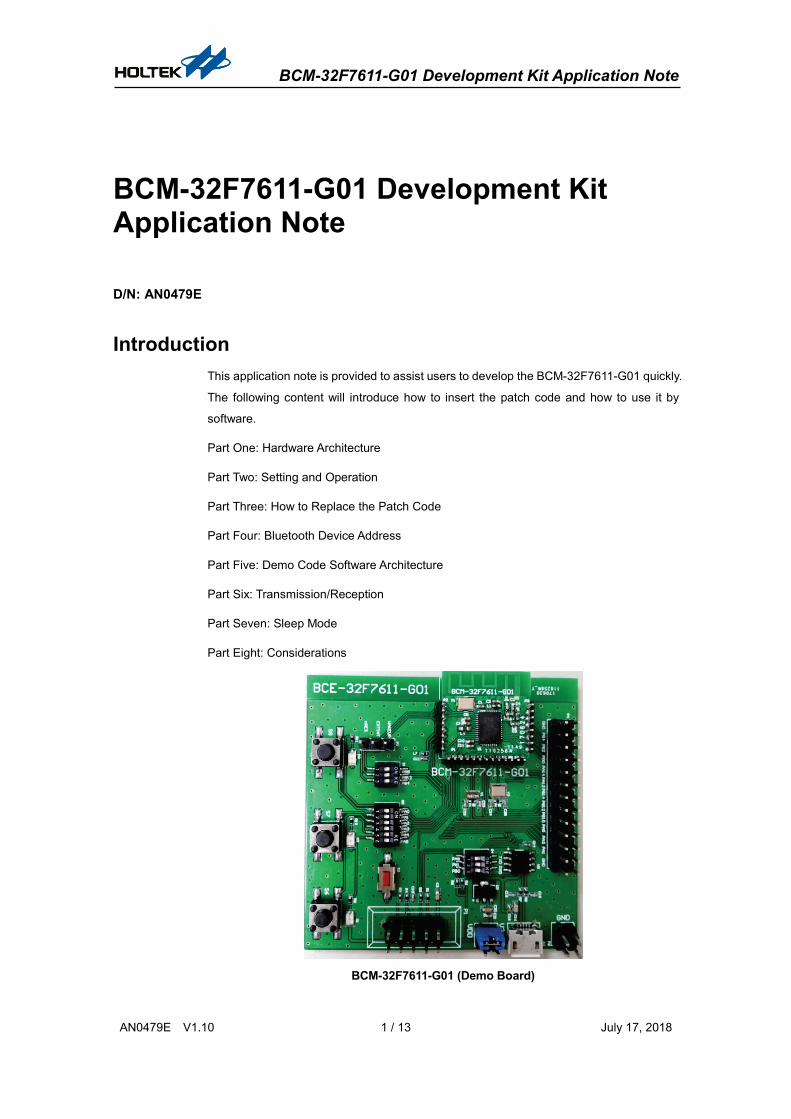
BCM-32F7611-G01 (Demo Board)
BCM-32F7611-G01 Development Kit Application Note
AN0479E V1.10 2 / 13 July 17, 2018
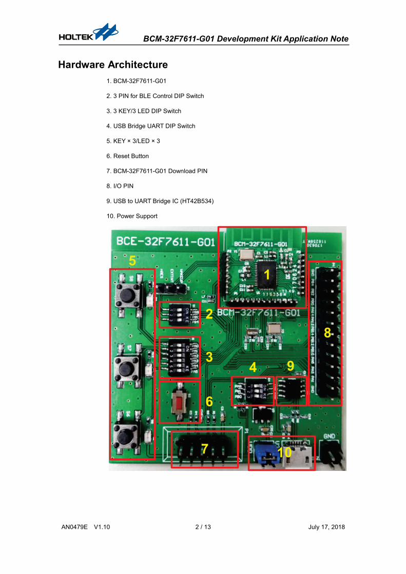
Hardware Architecture 1. BCM-32F7611-G01
2. 3 PIN for BLE Control DIP Switch
3. 3 KEY/3 LED DIP Switch
4. USB Bridge UART DIP Switch
5. KEY × 3/LED × 3
6. Reset Button
7. BCM-32F7611-G01 Download PIN
8. I/O PIN
9. USB to UART Bridge IC (HT42B534)
10. Power Support
1
8
4 9
7 10
6
3
2
5
BCM-32F7611-G01 Development Kit Application Note
AN0479E V1.10 3 / 13 July 17, 2018
Setting and Operation
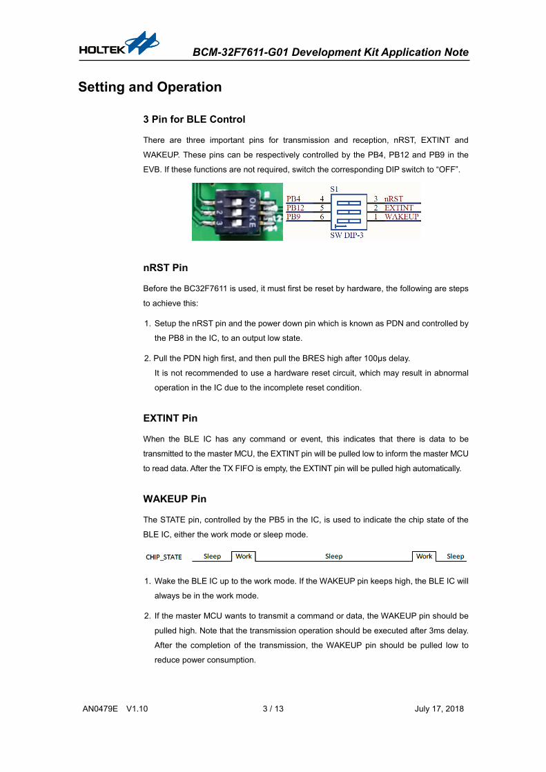
3 Pin for BLE Control
There are three important pins for transmission and reception, nRST, EXTINT and
WAKEUP. These pins can be respectively controlled by the PB4, PB12 and PB9 in the
EVB. If these functions are not required, switch the corresponding DIP switch to “OFF”.
nRST Pin
Before the BC32F7611 is used, it must first be reset by hardware, the following are steps
to achieve this:
1. Setup the nRST pin and the power down pin which is known as PDN and controlled by
the PB8 in the IC, to an output low state.
2. Pull the PDN high first, and then pull the BRES high after 100μs delay.
It is not recommended to use a hardware reset circuit, which may result in abnormal
operation in the IC due to the incomplete reset condition.
EXTINT Pin
When the BLE IC has any command or event, this indicates that there is data to be
transmitted to the master MCU, the EXTINT pin will be pulled low to inform the master MCU
to read data. After the TX FIFO is empty, the EXTINT pin will be pulled high automatically.
WAKEUP Pin
The STATE pin, controlled by the PB5 in the IC, is used to indicate the chip state of the
BLE IC, either the work mode or sleep mode.
1. Wake the BLE IC up to the work mode. If the WAKEUP pin keeps high, the BLE IC will
always be in the work mode.
2. If the master MCU wants to transmit a command or data, the WAKEUP pin should be
pulled high. Note that the transmission operation should be executed after 3ms delay.
After the completion of the transmission, the WAKEUP pin should be pulled low to
reduce power consumption.
BCM-32F7611-G01 Development Kit Application Note
AN0479E V1.10 4 / 13 July 17, 2018
The Mater MCU transmits data or CMD to the BLE IC
CHIP_STATE
WAKE_UP
WAKEUP Delay Sleep Delay
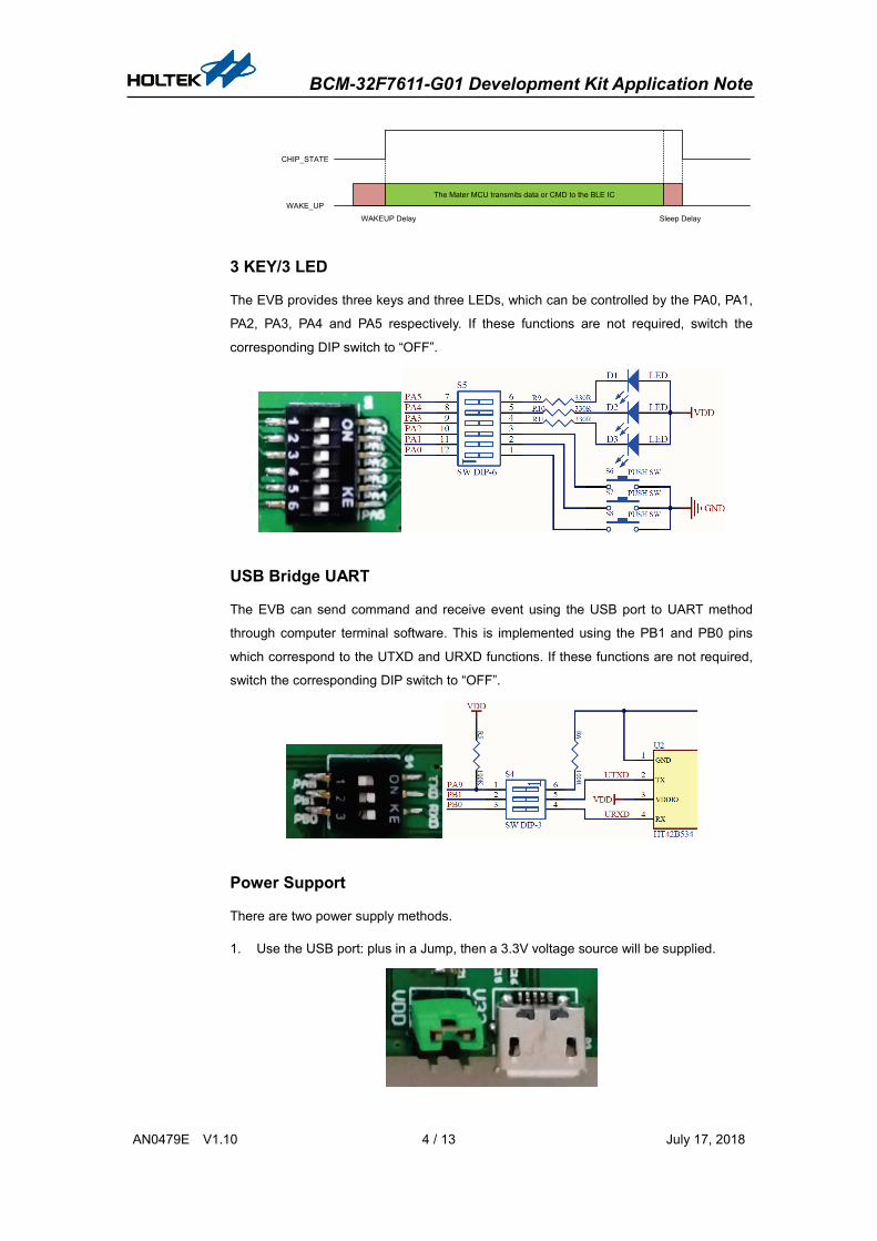
3 KEY/3 LED
The EVB provides three keys and three LEDs, which can be controlled by the PA0, PA1,
PA2, PA3, PA4 and PA5 respectively. If these functions are not required, switch the
corresponding DIP switch to “OFF”.
USB Bridge UART
The EVB can send command and receive event using the USB port to UART method
through computer terminal software. This is implemented using the PB1 and PB0 pins
which correspond to the UTXD and URXD functions. If these functions are not required,
switch the corresponding DIP switch to “OFF”.
Power Support
There are two power supply methods.
1. Use the USB port: plus in a Jump, then a 3.3V voltage source will be supplied.

BCM-32F7611-G01 Development Kit Application Note
AN0479E V1.10 5 / 13 July 17, 2018
2. External power supply: Connect the external positive DC power supply (VINmax =
3.6V) to the VDD pin and the external DC GND to the GND pin.
The following circuit diagram is provided for reference.
BCE-32F7611-G01 Schematic
How to Replace the Patch Code The user desired parameters can be setup using the “BLE Configuration Setting Tool”.
Refer to the “BLE Configuration Setting User’s Guide” for more details.
BCM-32F7611-G01 Development Kit Application Note
AN0479E V1.10 6 / 13 July 17, 2018
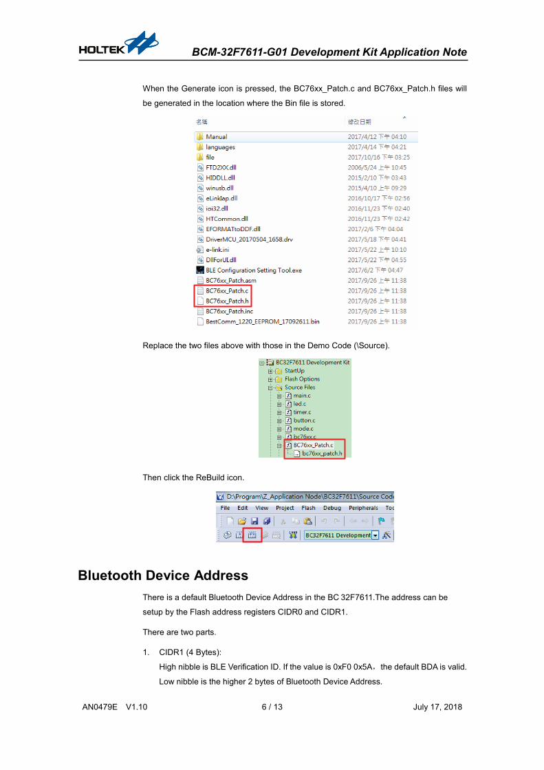
When the Generate icon is pressed, the BC76xx_Patch.c and BC76xx_Patch.h files will
be generated in the location where the Bin file is stored.
Replace the two files above with those in the Demo Code (\Source).
Then click the ReBuild icon.
Bluetooth Device Address There is a default Bluetooth Device Address in the BC 32F7611.The address can be
setup by the Flash address registers CIDR0 and CIDR1.
There are two parts.
1. CIDR1 (4 Bytes):
High nibble is BLE Verification ID. If the value is 0xF0 0x5A,the default BDA is valid.
Low nibble is the higher 2 bytes of Bluetooth Device Address.
BCM-32F7611-G01 Development Kit Application Note
AN0479E V1.10 7 / 13 July 17, 2018
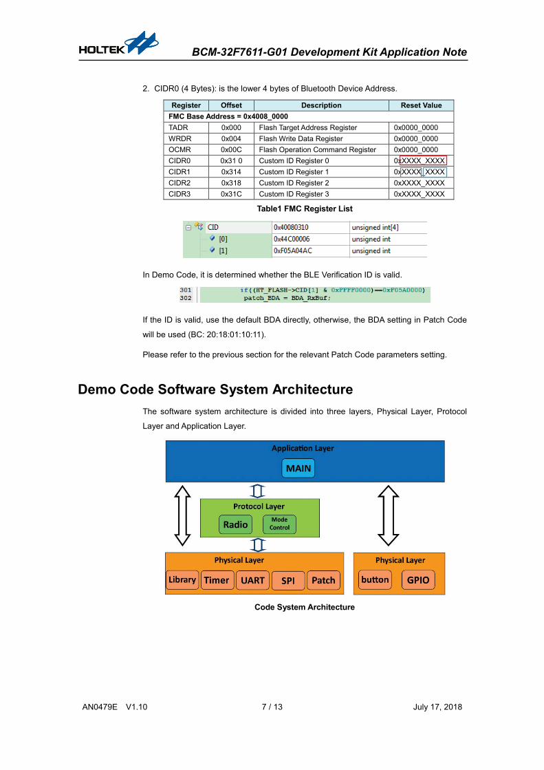
2. CIDR0 (4 Bytes): is the lower 4 bytes of Bluetooth Device Address.
Register Offset Description Reset Value FMC Base Address = 0x4008_0000 TADR 0x000 Flash Target Address Register 0x0000_0000 WRDR 0x004 Flash Write Data Register 0x0000_0000 OCMR 0x00C Flash Operation Command Register 0x0000_0000 CIDR0 0x31 0 Custom ID Register 0 0xXXXX_XXXX CIDR1 0x314 Custom ID Register 1 0xXXXX_XXXX CIDR2 0x318 Custom ID Register 2 0xXXXX_XXXX CIDR3 0x31C Custom ID Register 3 0xXXXX_XXXX
Table1 FMC Register List
In Demo Code, it is determined whether the BLE Verification ID is valid.
If the ID is valid, use the default BDA directly, otherwise, the BDA setting in Patch Code
will be used (BC: 20:18:01:10:11).
Please refer to the previous section for the relevant Patch Code parameters setting.
Demo Code Software System Architecture The software system architecture is divided into three layers, Physical Layer, Protocol
Layer and Application Layer.
Code System Architecture

BCM-32F7611-G01 Development Kit Application Note
AN0479E V1.10 8 / 13 July 17, 2018
This section will illustrate the functionality and programs of each layer in detail
Radio
Mode Control
Patch
Demo Code List
Physical Layer
Writing software/firmware is like building a building, the better programming the bottom
layer, the more stable the software/firmware. First introduce the SPI, and then describe
the processing programs of UART, Timer, Library, Button and GPIO, finally illustrate the
Patch processing program.
1. SPI Processing Program
The Command/Event transmission between the BC32F7611 internal MCU and RF is
carried out via the SPI interface. Therefore, it is a very important function. Even the RF
initialization is also implemented using the SPI.
2. UART Processing Program
The Development Kit can be connected to the Host computer through the HT42B534
via the USB port. Then the BC32F7611 transmission can be monitored by the Toolkit
via the COM port of the computer.
3. Timer Processing Program
The BFTM0 Timer can generate an interrupt every 1ms.
BCM-32F7611-G01 Development Kit Application Note
AN0479E V1.10 9 / 13 July 17, 2018
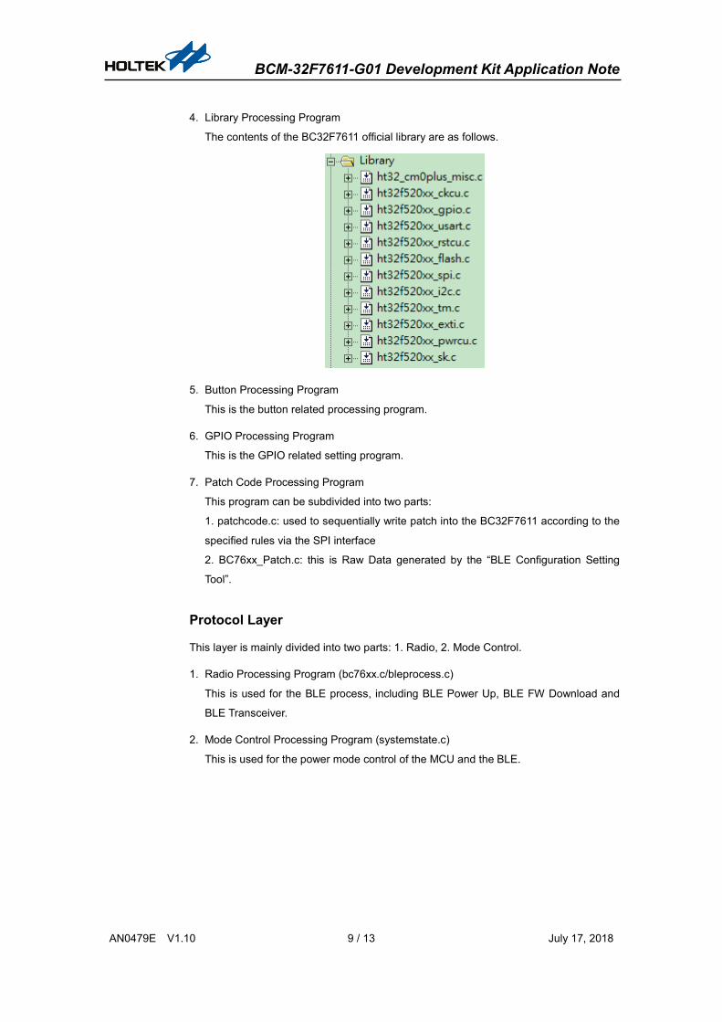
4. Library Processing Program
The contents of the BC32F7611 official library are as follows.
5. Button Processing Program
This is the button related processing program.
6. GPIO Processing Program
This is the GPIO related setting program.
7. Patch Code Processing Program
This program can be subdivided into two parts:
1. patchcode.c: used to sequentially write patch into the BC32F7611 according to the
specified rules via the SPI interface
2. BC76xx_Patch.c: this is Raw Data generated by the “BLE Configuration Setting
Tool”.
Protocol Layer
This layer is mainly divided into two parts: 1. Radio, 2. Mode Control.
1. Radio Processing Program (bc76xx.c/bleprocess.c)
This is used for the BLE process, including BLE Power Up, BLE FW Download and
BLE Transceiver.
2. Mode Control Processing Program (systemstate.c)
This is used for the power mode control of the MCU and the BLE.
BCM-32F7611-G01 Development Kit Application Note
AN0479E V1.10 10 / 13 July 17, 2018
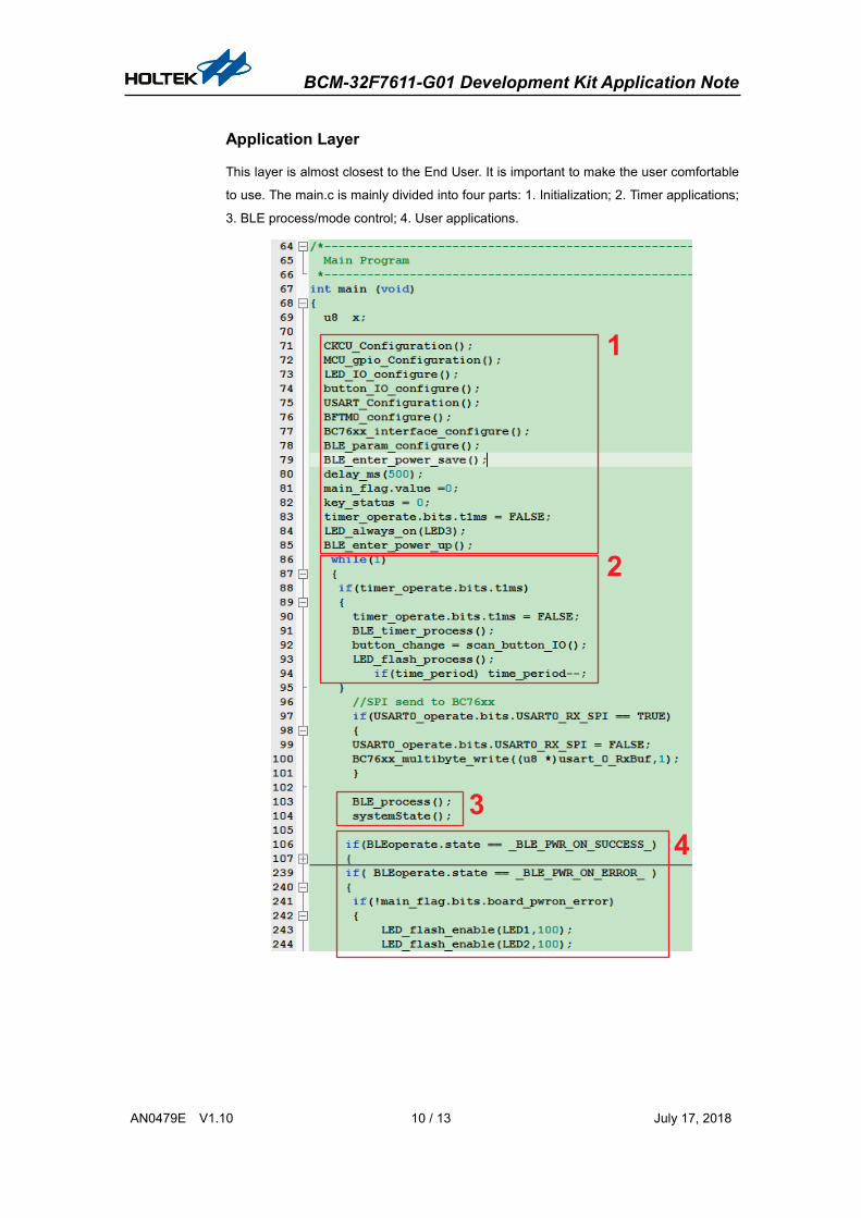
Application Layer
This layer is almost closest to the End User. It is important to make the user comfortable
to use. The main.c is mainly divided into four parts: 1. Initialization; 2. Timer applications;
3. BLE process/mode control; 4. User applications.
1
2
34
BCM-32F7611-G01 Development Kit Application Note
AN0479E V1.10 11 / 13 July 17, 2018
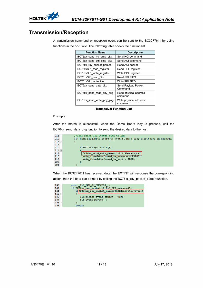
Transmission/Reception A transmission command or reception event can be sent to the BC32F7611 by using
functions in the bc76xx.c. The following table shows the function list.
Function Name Description BC76xx_send_hci_cmd_pkg Send HCI command BC76xx_send_ctrl_cmd_pkg Send ACI command BC76xx_rcv_packet_parser Read ACI packet BC76xxSPI_read_register Read SPI Register BC76xxSPI_write_register Write SPI Register BC76xxSPI_read_fifo Read SPI FIFO BC76xxSPI_write_fifo Write SPI FIFO BC76xx_send_data_pkg Send Payload Packet
Command BC76xx_send_read_phy_pkg Read physical address
command BC76xx_send_write_phy_pkg Write physical address
command
Transceiver Function List
Example:
After the match is successful, when the Demo Board Key is pressed, call the
BC76xx_send_data_pkg function to send the desired data to the host.
When the BC32F7611 has received data, the EXTINT will response the corresponding
action, then the data can be read by calling the BC76xx_rcv_packet_parser function.
BCM-32F7611-G01 Development Kit Application Note
AN0479E V1.10 12 / 13 July 17, 2018
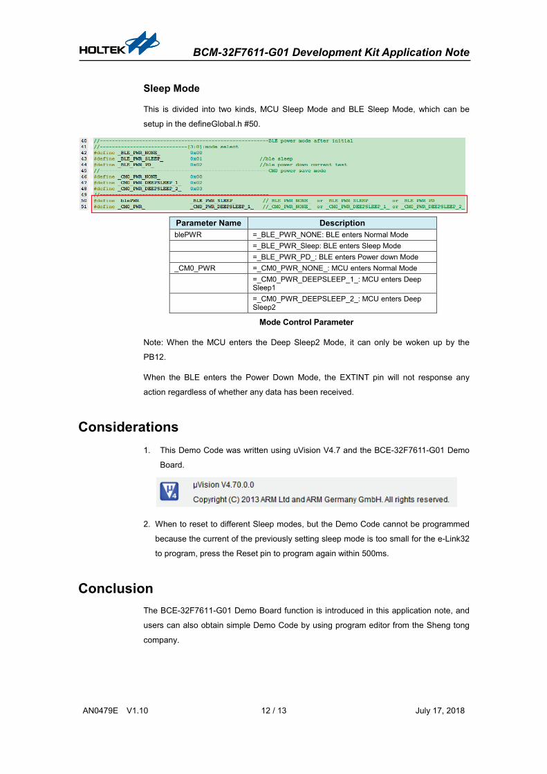
Sleep Mode
This is divided into two kinds, MCU Sleep Mode and BLE Sleep Mode, which can be
setup in the defineGlobal.h #50.
Parameter Name Description blePWR =_BLE_PWR_NONE: BLE enters Normal Mode =_BLE_PWR_Sleep: BLE enters Sleep Mode =_BLE_PWR_PD_: BLE enters Power down Mode _CM0_PWR =_CM0_PWR_NONE_: MCU enters Normal Mode =_CM0_PWR_DEEPSLEEP_1_: MCU enters Deep
Sleep1 =_CM0_PWR_DEEPSLEEP_2_: MCU enters Deep
Sleep2
Mode Control Parameter
Note: When the MCU enters the Deep Sleep2 Mode, it can only be woken up by the
PB12.
When the BLE enters the Power Down Mode, the EXTINT pin will not response any
action regardless of whether any data has been received.
Considerations 1. This Demo Code was written using uVision V4.7 and the BCE-32F7611-G01 Demo
Board.
2. When to reset to different Sleep modes, but the Demo Code cannot be programmed
because the current of the previously setting sleep mode is too small for the e-Link32
to program, press the Reset pin to program again within 500ms.
Conclusion The BCE-32F7611-G01 Demo Board function is introduced in this application note, and
users can also obtain simple Demo Code by using program editor from the Sheng tong
company.
BCM-32F7611-G01 Development Kit Application Note
AN0479E V1.10 13 / 13 July 17, 2018
Reference Files
Refer to the BC32F7611 DataSheet.
For more information, refer to the Holtek’s official website http://www.holtek.com.en.
Version and Modify Information Date Author Issue and Revision
2018.07.11 Harry Hsu (徐鸿文) V1.10. Update Hardware Architecture diagram.
2018.01.24 Harry Hsu (徐鸿文) V1.00
Disclaimer
All information, trademarks, logos, graphics, videos, audio clips, links and other items
appearing on this website ('Information') are for reference only and is subject to change at
any time without prior notice and at the discretion of Holtek Semiconductor Inc.
(hereinafter 'Holtek', 'the company', 'us', 'we' or 'our'). Whilst Holtek endeavors to ensure
the accuracy of the Information on this website, no express or implied warranty is given
by Holtek to the accuracy of the Information. Holtek shall bear no responsibility for any
incorrectness or leakage.
Holtek shall not be liable for any damages (including but not limited to computer virus,
system problems or data loss) whatsoever arising in using or in connection with the use of
this website by any party. There may be links in this area, which allow you to visit the
websites of other companies. These websites are not controlled by Holtek. Holtek will
bear no responsibility and no guarantee to whatsoever Information displayed at such sites.
Hyperlinks to other websites are at your own risk.
Limitation of Liability
In no event shall Holtek Limited be liable to any other party for any loss or damage
whatsoever or howsoever caused directly or indirectly in connection with your access to
or use of this website, the content thereon or any goods, materials or services.
Governing Law
The Disclaimer contained in the website shall be governed by and interpreted in
accordance with the laws of the Republic of China. Users will submit to the non-exclusive
jurisdiction of the Republic of China courts.
Update of Disclaimer Holtek reserves the right to update the Disclaimer at any time with or without prior notice,
all changes are effective immediately upon posting to the website.