
Basics and Practical Examples of...
21
Digital Design Seminar FOPE \DDS\Transmis.ppt Aug96 Basics and Practical Examples of Transmission
Transcript of Basics and Practical Examples of...
Digital Design Seminar
FOPE \DDS\Transmis.ppt Aug96
Basicsand
Practical Examples of Transmission
Digital Design Seminar
FOPE \DDS\Transmis.ppt Aug96
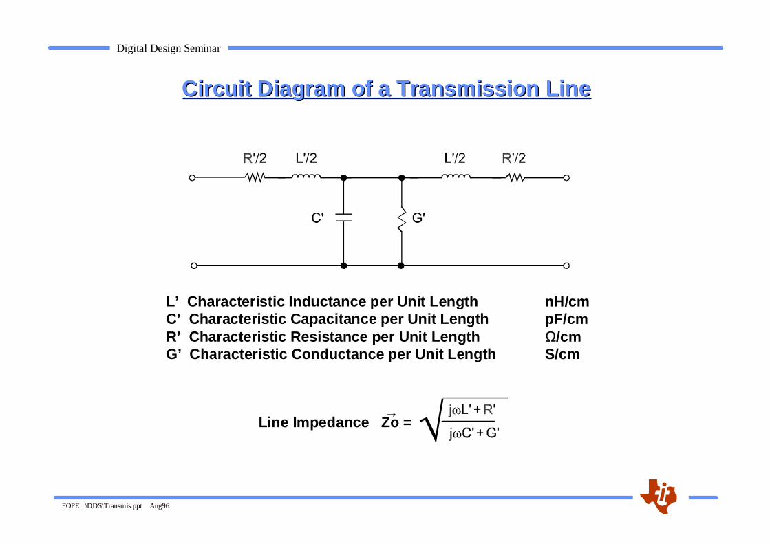
Circuit Diagram of a Transmission LineCircuit Diagram of a Transmission Line
L’ Characteristic Inductance per Unit LengthC’ Characteristic Capacitance per Unit LengthR’ Characteristic Resistance per Unit LengthG’ Characteristic Conductance per Unit Length
nH/cmpF/cmΩΩ/cmS/cm
Line Impedance Zo = →→
Digital Design Seminar
FOPE \DDS\Transmis.ppt Aug96
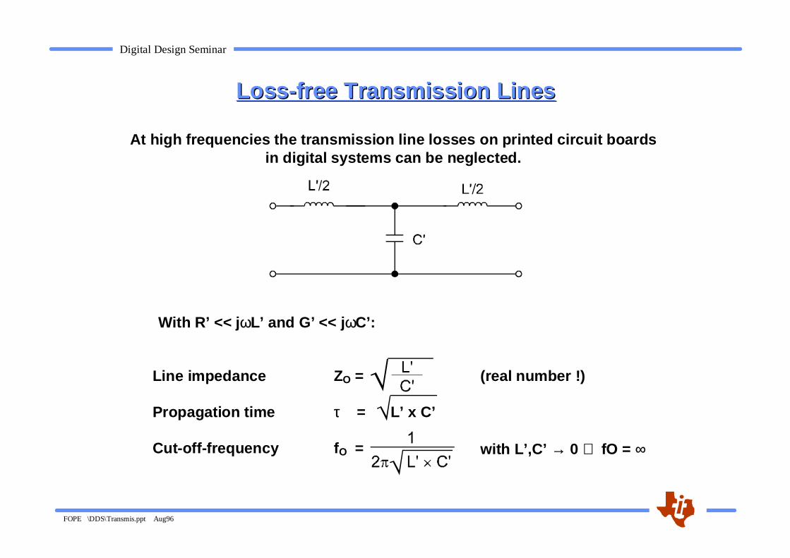
Loss-free Transmission LinesLoss-free Transmission Lines
At high frequencies the transmission line losses on printed circuit boardsin digital systems can be neglected.
With R’ << j ϖϖL’ and G’ << j ϖϖC’:
Line impedance
Propagation time
Cut-off-frequency
ZO =
τ τ = L’ x C’
fO =
(real number !)
with L’,C’ →→ 0 ⇒⇒ fO = ∞∞
Digital Design Seminar
FOPE \DDS\Transmis.ppt Aug96
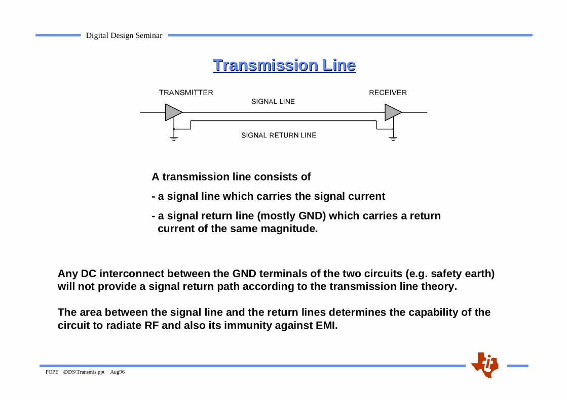
Transmission LineTransmission Line
A transmission line consists of
- a signal line which carries the signal current
- a signal return line (mostly GND) which carries a return current of the same magnitude.
Any DC interconnect between the GND terminals of the two circuits (e.g. safety earth)will not provide a signal return path according to the transmission line theory.
The area between the signal line and the return lines determines the capability of the circuit to radiate RF and also its immunity against EMI.
Digital Design Seminar
FOPE \DDS\Transmis.ppt Aug96
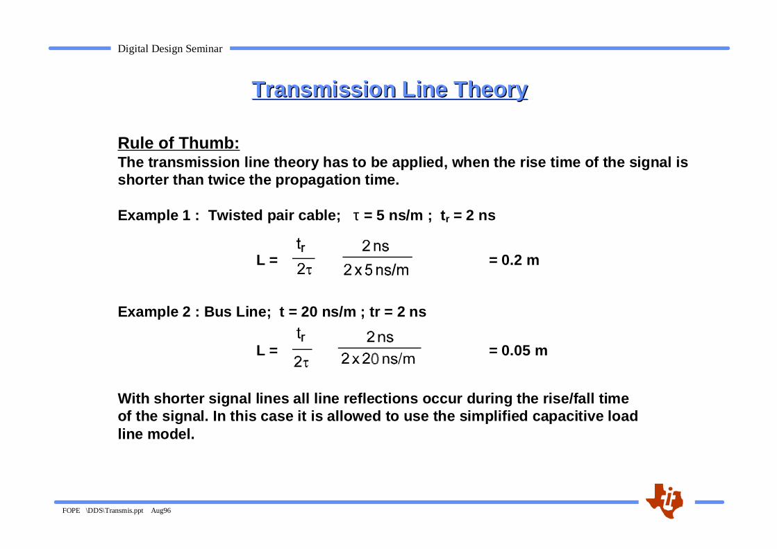
Transmission Line TheoryTransmission Line Theory
Rule of Thumb:The transmission line theory has to be applied, when the rise time of the signal isshorter than twice the propagation time.
Example 1 : Twisted pair cable; ττ = 5 ns/m ; t r = 2 ns
= 0.2 m
= 0.05 m
Example 2 : Bus Line; t = 20 ns/m ; tr = 2 ns
L =
L =
With shorter signal lines all line reflections occur during the rise/fall time of the signal. In this case it is allowed to use the simplified capacitive loadline model.
Digital Design Seminar
FOPE \DDS\Transmis.ppt Aug96
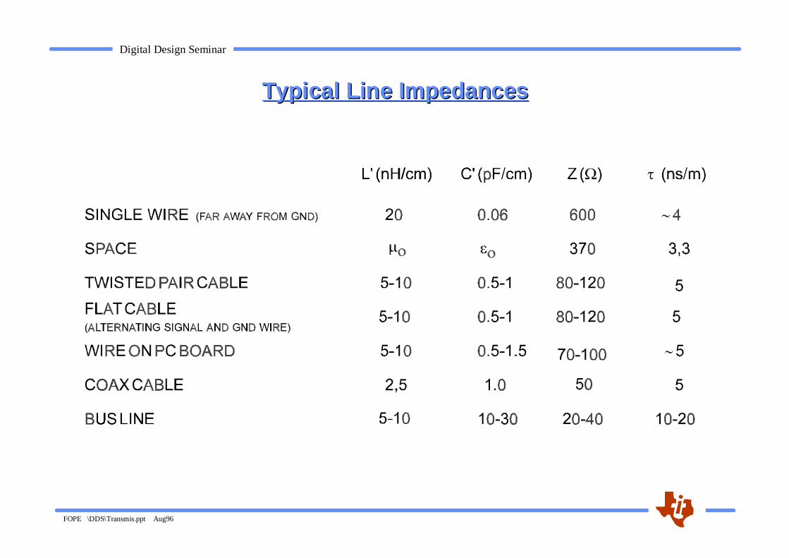
Typical Line ImpedancesTypical Line Impedances
Digital Design Seminar
FOPE \DDS\Transmis.ppt Aug96
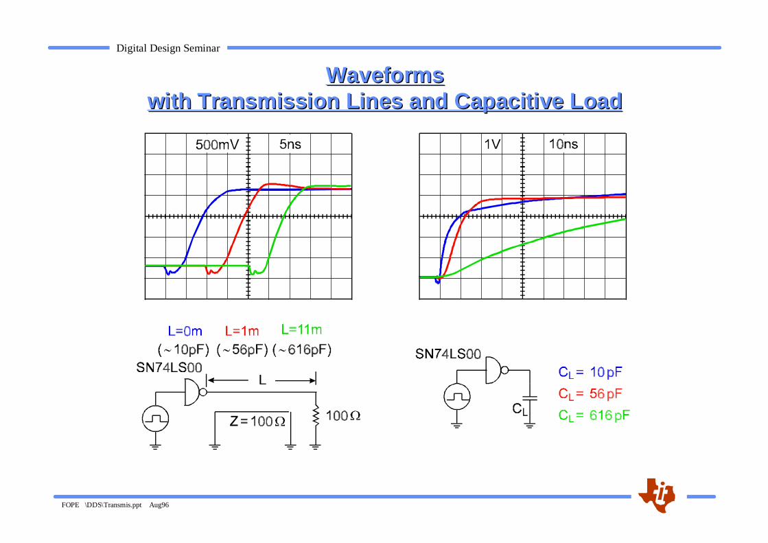
WaveformsWaveformswith Transmission Lines and Capacitive Loadwith Transmission Lines and Capacitive Load
Digital Design Seminar
FOPE \DDS\Transmis.ppt Aug96
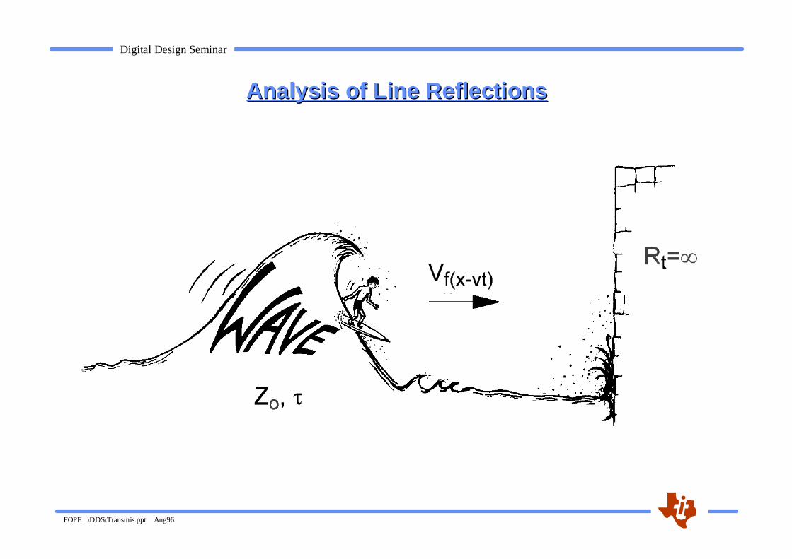
Analysis of Line ReflectionsAnalysis of Line Reflections
Digital Design Seminar
FOPE \DDS\Transmis.ppt Aug96
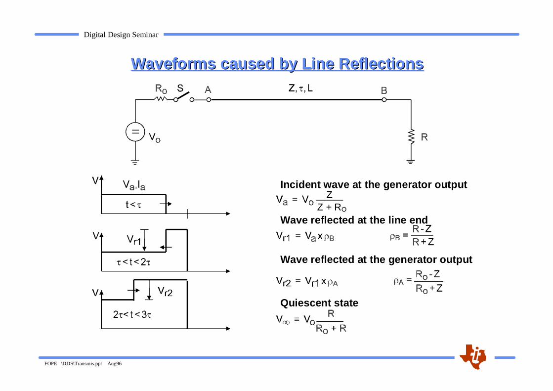
Waveforms caused by Line ReflectionsWaveforms caused by Line Reflections
Incident wave at the generator output
Wave reflected at the line end
Wave reflected at the generator output
Quiescent state
Z + RO
Digital Design Seminar
FOPE \DDS\Transmis.ppt Aug96
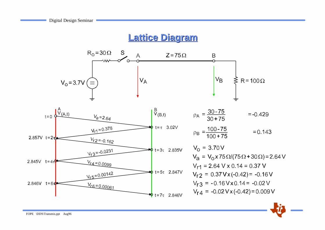
Lattice DiagramLattice Diagram
Digital Design Seminar
FOPE \DDS\Transmis.ppt Aug96
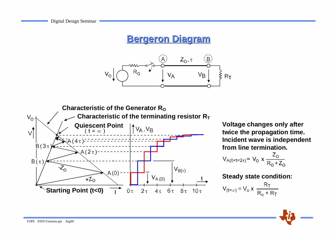
Bergeron DiagramBergeron Diagram
Voltage changes only aftertwice the propagation time.Incident wave is independentfrom line termination.
Characteristic of the Generator R O
Characteristic of the terminating resistor R T
Quiescent Point
Starting Point (t<0)
Steady state condition:
Digital Design Seminar
FOPE \DDS\Transmis.ppt Aug96
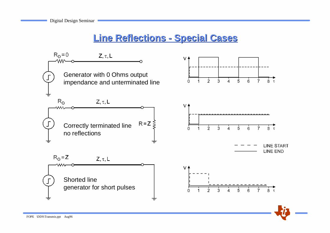
Line Reflections - Special CasesLine Reflections - Special Cases
Generator with 0 Ohms outputimpendance and unterminated line
Correctly terminated lineno reflections
Shorted linegenerator for short pulses
Digital Design Seminar
FOPE \DDS\Transmis.ppt Aug96
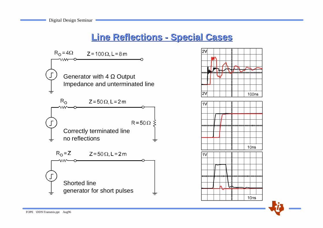
Line Reflections - Special CasesLine Reflections - Special Cases
Generator with 4 Ω OutputImpedance and unterminated line
Correctly terminated lineno reflections
Shorted linegenerator for short pulses
Digital Design Seminar
FOPE \DDS\Transmis.ppt Aug96
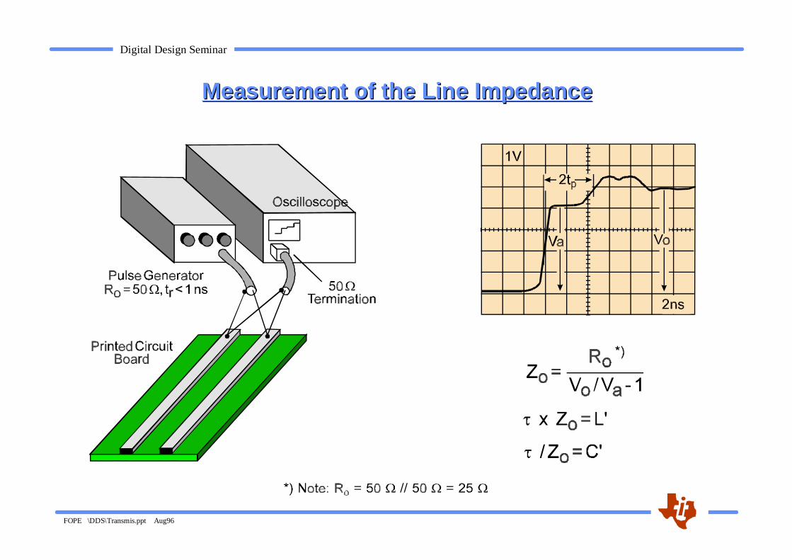
Measurement of the Line ImpedanceMeasurement of the Line Impedance
Digital Design Seminar
FOPE \DDS\Transmis.ppt Aug96
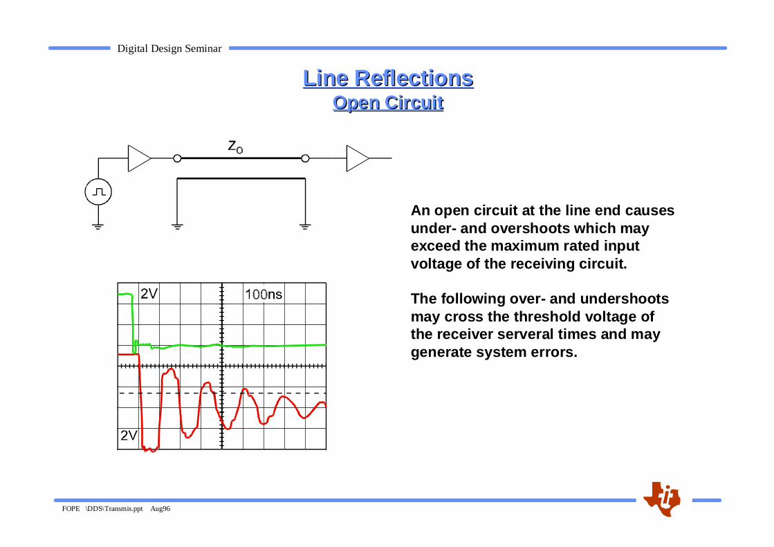
Line ReflectionsLine ReflectionsOpen CircuitOpen Circuit
An open circuit at the line end causesunder- and overshoots which may exceed the maximum rated inputvoltage of the receiving circuit.
The following over- and undershootsmay cross the threshold voltage ofthe receiver serveral times and maygenerate system errors.
Digital Design Seminar
FOPE \DDS\Transmis.ppt Aug96
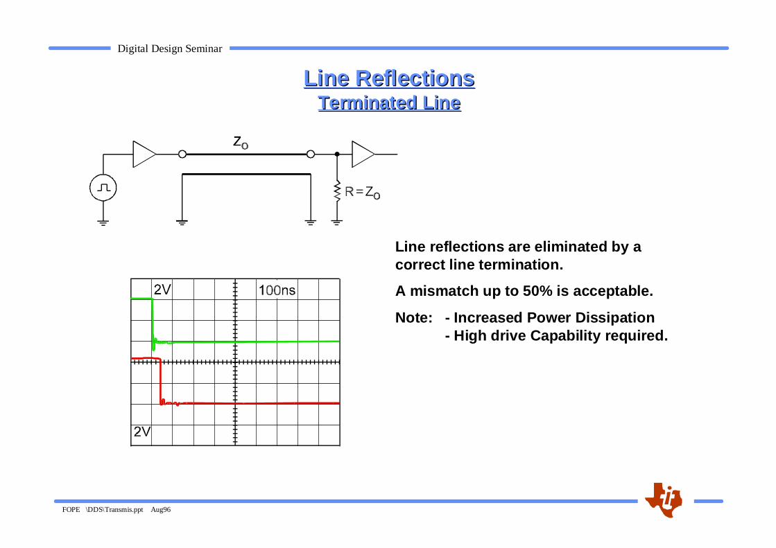
Line ReflectionsLine ReflectionsTerminated LineTerminated Line
Line reflections are eliminated by acorrect line termination.
A mismatch up to 50% is acceptable.
Note: - Increased Power Dissipation- High drive Capability required.
Digital Design Seminar
FOPE \DDS\Transmis.ppt Aug96
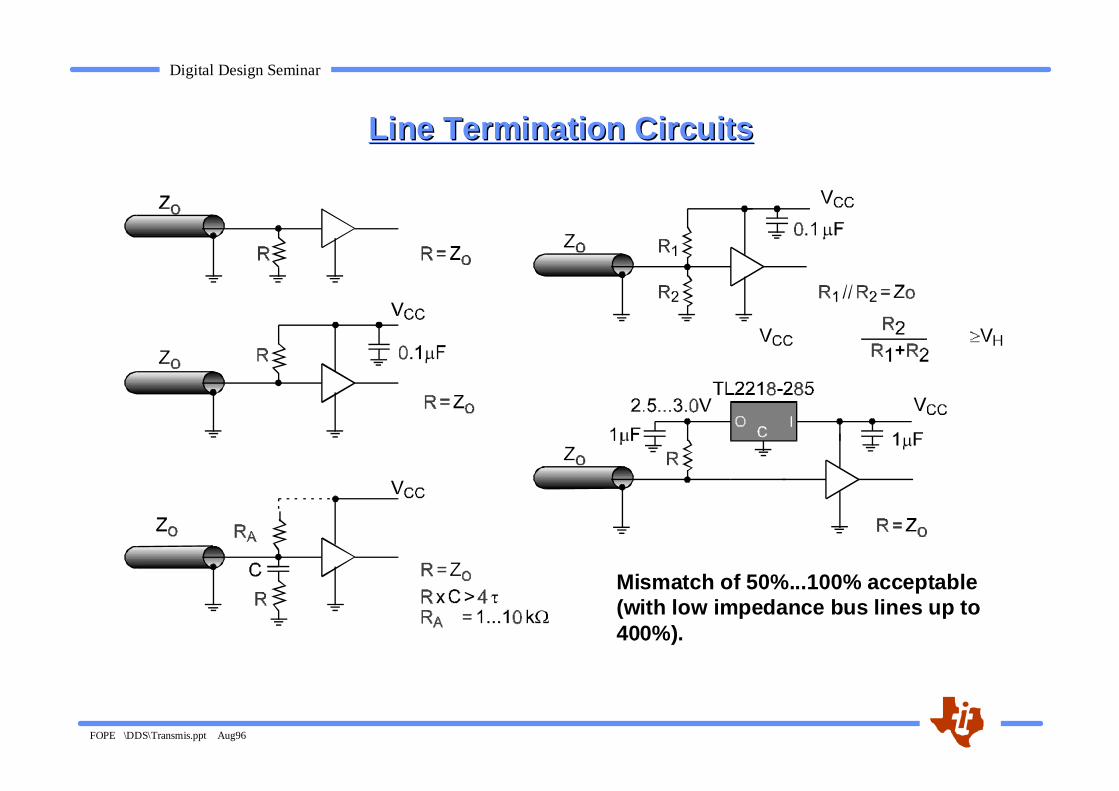
Line Termination CircuitsLine Termination Circuits
Mismatch of 50%...100% acceptable(with low impedance bus lines up to 400%).
Digital Design Seminar
FOPE \DDS\Transmis.ppt Aug96
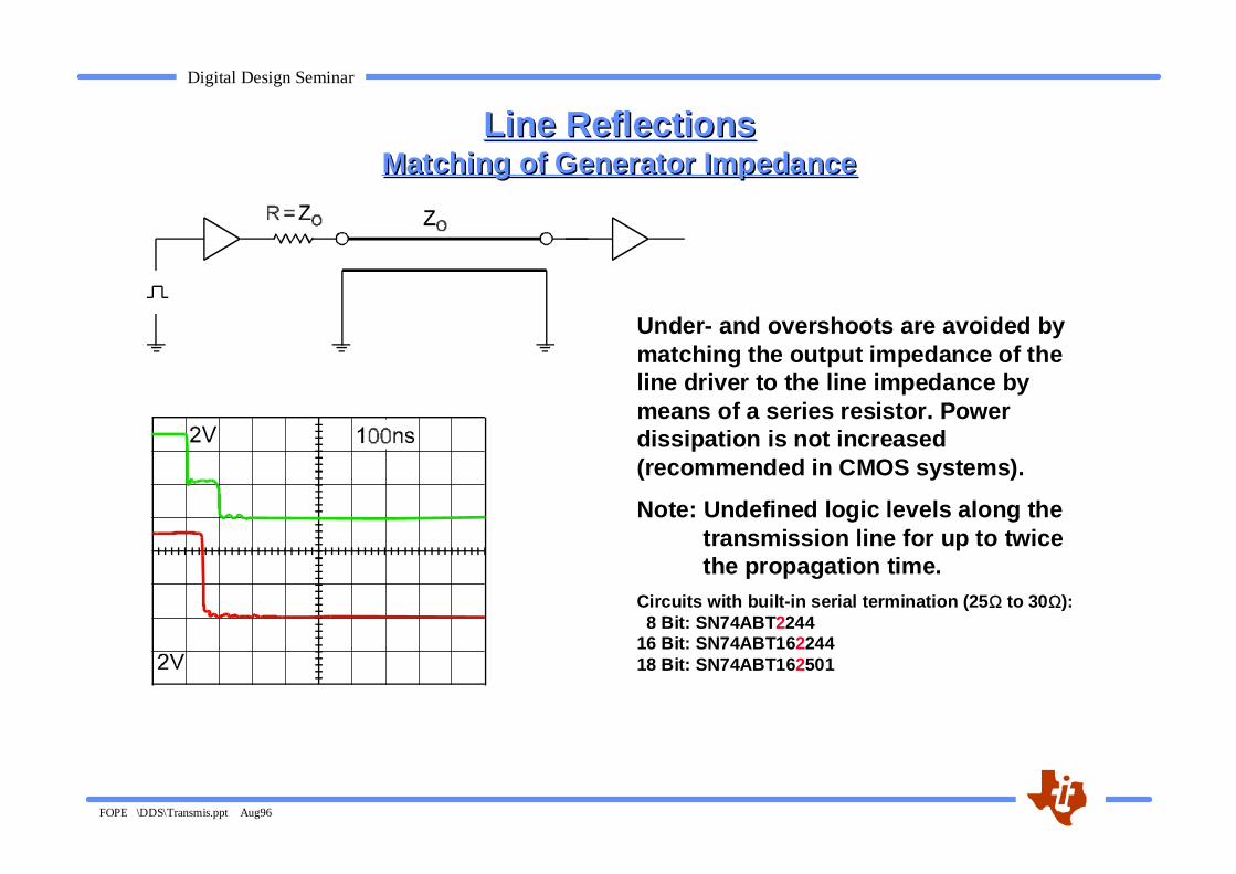
Line ReflectionsLine ReflectionsMatching of Generator ImpedanceMatching of Generator Impedance
Under- and overshoots are avoided bymatching the output impedance of theline driver to the line impedance bymeans of a series resistor. Powerdissipation is not increased(recommended in CMOS systems).
Note: Undefined logic levels along thetransmission line for up to twicethe propagation time.
Circuits with built-in serial termination (25 ΩΩ to 30 ΩΩ): 8 Bit: SN74ABT 224416 Bit: SN74ABT16 224418 Bit: SN74ABT16 2501
Digital Design Seminar
FOPE \DDS\Transmis.ppt Aug96
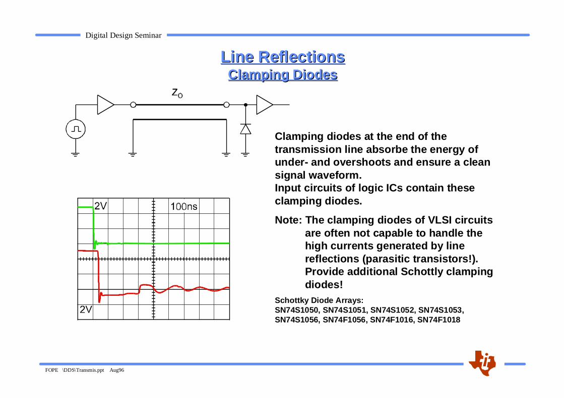
Line ReflectionsLine ReflectionsClamping DiodesClamping Diodes
Clamping diodes at the end of thetransmission line absorbe the energy ofunder- and overshoots and ensure a cleansignal waveform.Input circuits of logic ICs contain theseclamping diodes.
Note: The clamping diodes of VLSI circuitsare often not capable to handle thehigh currents generated by line reflections (parasitic transistors!).Provide additional Schottly clampingdiodes!
Schottky Diode Arrays:SN74S1050, SN74S1051, SN74S1052, SN74S1053,SN74S1056, SN74F1056, SN74F1016, SN74F1018
Digital Design Seminar
FOPE \DDS\Transmis.ppt Aug96
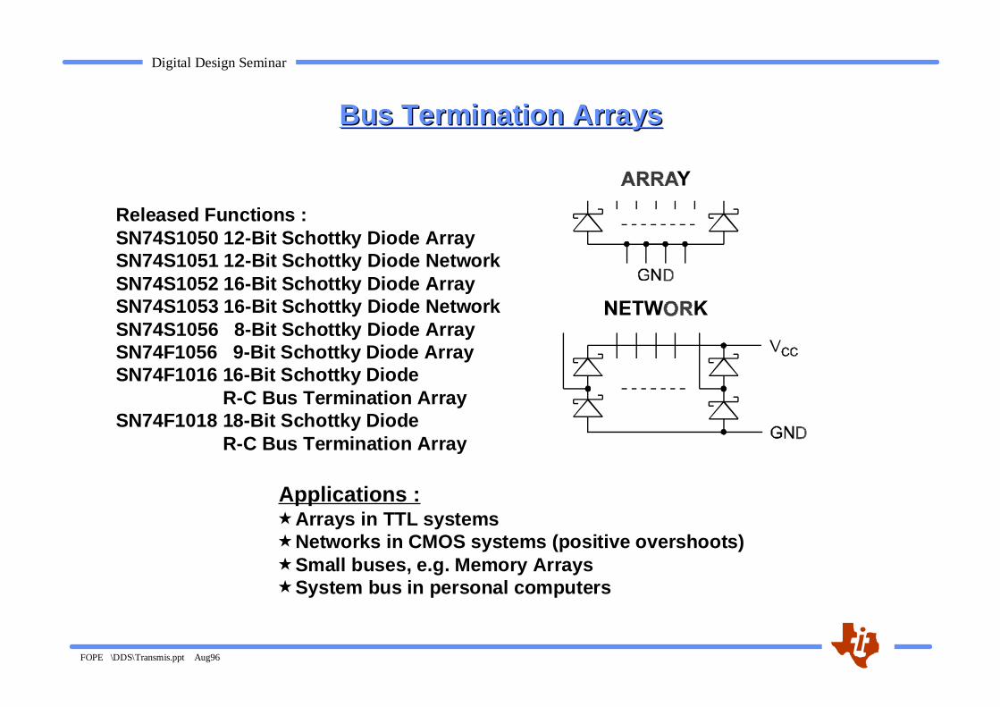
Bus Termination ArraysBus Termination Arrays
Applications :Arrays in TTL systemsNetworks in CMOS systems (positive overshoots)Small buses, e.g. Memory ArraysSystem bus in personal computers
Released Functions :SN74S1050 12-Bit Schottky Diode ArraySN74S1051 12-Bit Schottky Diode NetworkSN74S1052 16-Bit Schottky Diode ArraySN74S1053 16-Bit Schottky Diode NetworkSN74S1056 8-Bit Schottky Diode ArraySN74F1056 9-Bit Schottky Diode ArraySN74F1016 16-Bit Schottky Diode
R-C Bus Termination ArraySN74F1018 18-Bit Schottky Diode
R-C Bus Termination Array
Digital Design Seminar
FOPE \DDS\Transmis.ppt Aug96
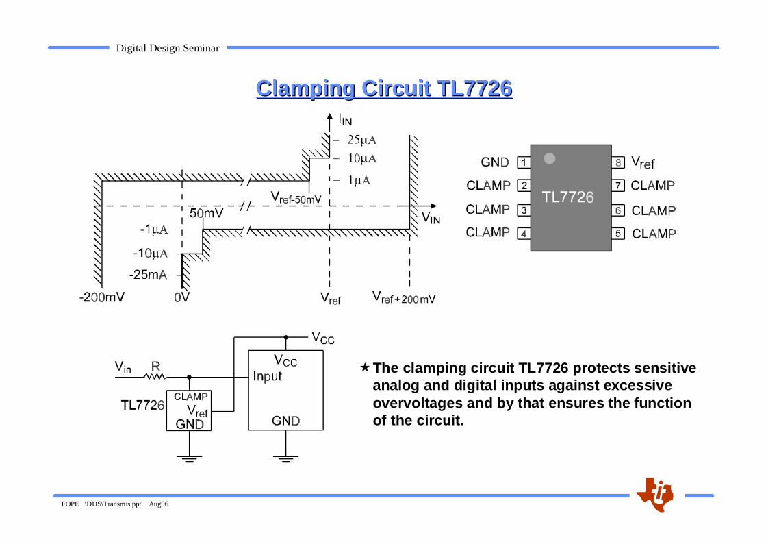
Clamping Circuit TL7726Clamping Circuit TL7726
The clamping circuit TL7726 protects sensitiveanalog and digital inputs against excessive overvoltages and by that ensures the functionof the circuit.