-based Charge-trapping synaptic device with 2 electrical ...
12
Research article Min Zhang a , Zehui Fan a , Xixi Jiang, Hao Zhu*, Lin Chen*, Yidong Xia*, Jiang Yin, Xinke Liu, Qingqing Sun and David Wei Zhang MoS 2 -based Charge-trapping synaptic device with electrical and optical modulated conductance https://doi.org/10.1515/nanoph-2019-0548 Received December 25, 2019; revised January 31, 2020; accepted January 31, 2020 Abstract: The synapse is one of the fundamental elements in human brain performing functions such as learning, memorizing, and visual processing. The implementation of synaptic devices to realize neuromorphic computing and sensing tasks is a key step to artificial intelligence, which, however, has been bottlenecked by the complex circuitry and device integration. We report a high-perfor- mance charge-trapping memory synaptic device based on two-dimensional (2D) MoS 2 and high-k Ta 2 O 5 –TiO 2 (TTO) composite to build efficient and reliable neuromorphic system, which can be modulated by both electrical and optical stimuli. Significant and essential synaptic behav- iors including short-term plasticity, long-term potentia- tion, and long-term depression have been emulated. Such excellent synaptic behaviors originated from the good nonvolatile memory performance due to the high den- sity of defect states in the engineered TTO composite. The 2D synaptic device also exhibits effective switching by incident light tuning, which further enables pattern recognition with accuracy rate reaching 100%. Such experimental demonstration paves a robust way toward a multitask neuromorphic system and opens up potential applications in future artificial intelligence and sensing technology. Keywords: MoS 2 ; composite dielectric; nonvolatile memory; synaptic device; ANN. The rapidly evolving computing science and technology have urged more unexploited data processing modes to be fast tracked for the development and deployment in the field of artificial intelligence [1–4]. Traditional computing systems based on von Neumann architecture have lost the edge and become inefficient when dealing with increas- ingly complex problems such as speech, image, and video data processing, which often need huge physical resources and enormous energy consumption [5–7]. On the other hand, the human brain, which consists of a highly inter- connected and massively parallel network, is an efficient information processing and storage system [8]. The 10 11 neurons in the brain are responsible for the cognition and calculation, and the 10 15 synapses are the critical units in signal delivery and processing [9, 10]. Synaptic behaviors including short-term plasticity (STP), long-term potentia- tion (LTP), and long-term depression (LTD) function in the biological brain for memory and actions, and the human learning behaviors are achieved by modulating the weight of synapse through spike controlling. Therefore, great efforts have been made to realize an artificial brain-like network based on the biological synaptic plasticity to process tremendous data in various forms with faster speed and lower power consumption [11]. So far, different prototypes of synaptic devices have been developed emulating synaptic dynamics toward the implementation of brain-like computing and data process- ing systems, such as conductive bridging (CBRAM) [12–14], resistive change memory [15, 16], and phase change memory [17, 18]. Most of the reported synaptic devices are based on passive and two-terminal structures similar to a Min Zhang and Zehui Fan: These authors contributed equally to this work. *Corresponding author: Hao Zhu and Lin Chen, State Key Laboratory of ASIC and System, School of Microelectronics, Fudan University, Shanghai 200433, China, e-mail: [email protected] (H. Zhu); [email protected] (L. Chen). https://orcid.org/0000-0002-7145- 7564 (L. Chen); and Yidong Xia, College of Engineering and Applied Science, Nanjing University, Nanjing, 210093, China, e-mail: xiayd@ nju.edu.cn Min Zhang: State Key Laboratory of ASIC and System, School of Microelectronics, Fudan University, Shanghai 200433, China; and School of Mathematics, Physics and Information Engineering, Jiaxing University, Jiaxing 314001, China Zehui Fan, Xixi Jiang, Qingqing Sun and David Wei Zhang: State Key Laboratory of ASIC and System, School of Microelectronics, Fudan University, Shanghai 200433, China Jiang Yin: College of Engineering and Applied Science, Nanjing University, Nanjing, 210093, China Xinke Liu: College of Materials Science and Engineering, Shenzhen University, Shenzhen 518060, China. https://orcid.org/0000-0002- 3472-5945 Open Access. © 2020 Hao Zhu, Lin Chen, Yidong Xia et al., published by De Gruyter. This work is licensed under the Creative Commons Attribu- tion 4.0 Public License. Nanophotonics 2020; 9(8): 2475–2486
Transcript of -based Charge-trapping synaptic device with 2 electrical ...
Research article
Min Zhanga, Zehui Fana, Xixi Jiang, Hao Zhu*, Lin Chen*, Yidong Xia*, Jiang Yin, Xinke Liu, Qingqing Sun and David Wei Zhang
MoS2-based Charge-trapping synaptic device with electrical and optical modulated conductancehttps://doi.org/10.1515/nanoph-2019-0548Received December 25, 2019; revised January 31, 2020; accepted January 31, 2020
Abstract: The synapse is one of the fundamental elements in human brain performing functions such as learning, memorizing, and visual processing. The implementation of synaptic devices to realize neuromorphic computing and sensing tasks is a key step to artificial intelligence, which, however, has been bottlenecked by the complex circuitry and device integration. We report a high-perfor-mance charge-trapping memory synaptic device based on two-dimensional (2D) MoS2 and high-k Ta2O5–TiO2 (TTO) composite to build efficient and reliable neuromorphic system, which can be modulated by both electrical and optical stimuli. Significant and essential synaptic behav-iors including short-term plasticity, long-term potentia-tion, and long-term depression have been emulated. Such excellent synaptic behaviors originated from the good nonvolatile memory performance due to the high den-sity of defect states in the engineered TTO composite. The 2D synaptic device also exhibits effective switching
by incident light tuning, which further enables pattern recognition with accuracy rate reaching 100%. Such experimental demonstration paves a robust way toward a multitask neuromorphic system and opens up potential applications in future artificial intelligence and sensing technology.
Keywords: MoS2; composite dielectric; nonvolatile memory; synaptic device; ANN.
The rapidly evolving computing science and technology have urged more unexploited data processing modes to be fast tracked for the development and deployment in the field of artificial intelligence [1–4]. Traditional computing systems based on von Neumann architecture have lost the edge and become inefficient when dealing with increas-ingly complex problems such as speech, image, and video data processing, which often need huge physical resources and enormous energy consumption [5–7]. On the other hand, the human brain, which consists of a highly inter-connected and massively parallel network, is an efficient information processing and storage system [8]. The 1011 neurons in the brain are responsible for the cognition and calculation, and the 1015 synapses are the critical units in signal delivery and processing [9, 10]. Synaptic behaviors including short-term plasticity (STP), long-term potentia-tion (LTP), and long-term depression (LTD) function in the biological brain for memory and actions, and the human learning behaviors are achieved by modulating the weight of synapse through spike controlling. Therefore, great efforts have been made to realize an artificial brain-like network based on the biological synaptic plasticity to process tremendous data in various forms with faster speed and lower power consumption [11].
So far, different prototypes of synaptic devices have been developed emulating synaptic dynamics toward the implementation of brain-like computing and data process-ing systems, such as conductive bridging (CBRAM) [12–14], resistive change memory [15, 16], and phase change memory [17, 18]. Most of the reported synaptic devices are based on passive and two-terminal structures similar to
aMin Zhang and Zehui Fan: These authors contributed equally to this work.*Corresponding author: Hao Zhu and Lin Chen, State Key Laboratory of ASIC and System, School of Microelectronics, Fudan University, Shanghai 200433, China, e-mail: [email protected] (H. Zhu); [email protected] (L. Chen). https://orcid.org/0000-0002-7145-7564 (L. Chen); and Yidong Xia, College of Engineering and Applied Science, Nanjing University, Nanjing, 210093, China, e-mail: [email protected] Min Zhang: State Key Laboratory of ASIC and System, School of Microelectronics, Fudan University, Shanghai 200433, China; and School of Mathematics, Physics and Information Engineering, Jiaxing University, Jiaxing 314001, ChinaZehui Fan, Xixi Jiang, Qingqing Sun and David Wei Zhang: State Key Laboratory of ASIC and System, School of Microelectronics, Fudan University, Shanghai 200433, ChinaJiang Yin: College of Engineering and Applied Science, Nanjing University, Nanjing, 210093, ChinaXinke Liu: College of Materials Science and Engineering, Shenzhen University, Shenzhen 518060, China. https://orcid.org/0000-0002-3472-5945
Open Access. © 2020 Hao Zhu, Lin Chen, Yidong Xia et al., published by De Gruyter. This work is licensed under the Creative Commons Attribu-tion 4.0 Public License.
Nanophotonics 2020; 9(8): 2475–2486
that of resistive random access memory (RRAM) due to the difficulty in obtaining multiple and distinguished conduc-tive states in transistor-based architecture [19]. In addi-tion, conventional semiconductors or functional films in the synaptic devices are designed and engineered to perform limited functions. Nevertheless, this has become increasingly incapable of fulfilling multitask with the development of various portable electronic devices such as image/video process and object detection. Therefore, the integration of functional materials with features such as optoelectronic properties as the active component in synaptic device is very attractive because it will leverage the advantages afforded by the new materials with the vast infrastructure of the synaptic electronics.
As a stable and repeatable physical mechanism, charge trapping has been widely applied in building non-volatile memory devices with good data retention. Such memory is based on the trapping and detrapping of elec-trons/holes in the charge storage medium changing the switching threshold. The charge-trapping memory (CTM) in field-effect transistor (FET)–like three-terminal archi-tecture has also been used in realizing artificial synapses as the amount of trapped charges can be effectively con-trolled through the operation voltage and device structure engineering to avoid the blurring between conductive states. But in terms of programming speed, conventional charge-trapping synaptic devices are largely limited by the trapping/releasing process of the charges because of the low trapping efficiency and unsuitable band offsets with respect to Si in traditional nitride or oxide films. Exploration focusing on the optimization of trapping mechanism and the engineering of the dielectric stack is critical to improve the trapping efficiency and opera-tion speed while maintaining good reliability. An addi-tional and effective strategy to achieve miniaturized yet performance-enhanced memory is to utilize atomically thin two-dimensional (2D) semiconductors as the active channel, which have been widely used in various fields [20–23]. Two-dimensional materials such as bilayer gra-phene, anisotropic black phosphorus (BP), and transition metal dichalcogenides (TMDs) have been integrated in FET-based synaptic devices with reinforced gate control and suppressed short-channel effects [24–27]. Tian et al. [28] reported a highly compact BP-based synaptic transis-tor emulating a biological axon–multisynapse network with connection heterogeneity to demonstrate an artificial anisotropic axon–multisynapse network. Liu et al. [29] reported a quasi-nonvolatile memory based on 2D materi-als with greatly enhanced writing speed, which is approx-imately 106 times faster than other memories. However, a crucial issue lies in the design and processing of the
dielectric/2D material interface, where a large number of defects and traps may exist because of the absence of dangling bonds on most layered semiconductors. This can significantly deteriorate the switching capabilities and the control over the charge-trapping process. Here, we report the fabrication and characterization of an arti-ficial synapse based on the flash-like CTM device using 2D MoS2, a typical TMD semiconductor as the channel and (Ta2O5)x(TiO2)1−x composite charge-trapping dielec-tric. Back-gate FET geometry with engineered gate stack ensures sufficient optical contrast for the identification of MoS2 flakes with least dielectric/MoS2 interface traps. Dif-ferent from the limited trapping sites with various energy levels in conventional single-material charge-trapping layer, the high density of defect states formed due to the interdiffusion between the two kinds of high-k oxides of Ta2O5 and TiO2 is responsible for the charge storage. Charge-trapping efficiency, programming/erasing speed, and retention capability have been greatly improved because of the PBCB (potentials at the bottom of con-duction band) between MoS2 and high-k composite. This provides a solid basis for the plasticity study in which the STP, LTP, and LTD behaviors have been successfully emu-lated. A near-perfect recognition rate has been achieved in the artificial neural network (ANN) built in this work. Furthermore, 2D materials are photosensitive [30–33] and have been explored in many optoelectronic applications [34–36]. Thus, synaptic functions have been effectively modulated by a series of optical operations owing to the robust optoelectronic properties in MoS2 and the engi-neered dielectric stack. Such control and tuning of the memory performance and synaptic behaviors pave attrac-tive ways toward the design of new synaptic devices for future neuromorphic computing and advanced sensing applications.
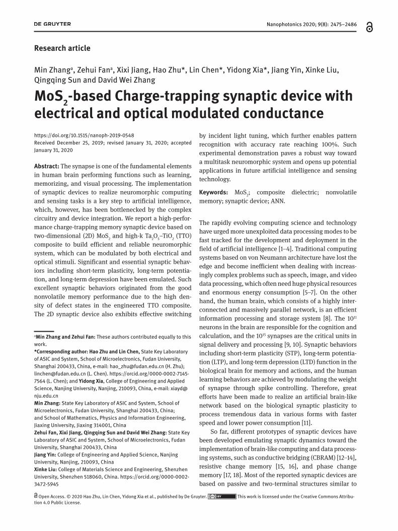
The structure of the back-gate MoS2 synaptic FET is schematically shown in Figure 1A. The ultrathin MoS2 channel is mechanically exfoliated from bulk and trans-ferred to the top surface of the back-gate stack. In the most reported experimental work on MoS2 transistors, the exfo-liated 2D flakes are generally transferred onto the relatively thick (~300 nm) SiO2 surface to gain sufficient contrast for the optical identification of the location, thickness, and lateral size of the flakes. However, such a thick dielectric layer will inevitably degrade the gate control over the channel and require a much higher operation voltage level. Alternatively, we employed an engineered Al2O3/(Ta2O5)x(TiO2)1−x (TTO)/Al2O3/indium tin oxide (ITO)/SiO2/Si stack in which the ITO works as the back-gate electrode with Al2O3/TTO/Al2O3 gate dielectric (see Methods for experimental details). Such engineered back-gate stack
2476 M. Zhang et al.: MoS2-based Charge-trapping synaptic device
can enable similar optical contrast as that on the 300-nm SiO2/Si substrate while significantly enhancing the gate control over the channel because of the thinner dielectric layers. The 4-nm Al2O3, 5-nm TTO, and 15-nm Al2O3 func-tion as the tunneling layer, charge-trapping layer, and blocking layer, respectively. Figure 1B shows the exfoliated MoS2 flakes on the top surface of the engineered stack. Good optical contrast between the ultrathin flake and the substrate with clear MoS2 edges has been achieved. From the cross-sectional transmission electron microscopy (TEM) image shown in Figure 1C, the gate stack has been successfully prepared with sharp interfaces between the MoS2 and the dielectric layers. The thickness of the MoS2 flake is ~2.9 nm corresponding to a 4-layer film. As men-tioned above, as the MoS2 channel region is prepared after the formation of gate stack, no dielectric deposition on the
MoS2 surface is involved, which is favorable to minimize the negative effects originated from the MoS2/Al2O3 inter-face traps.
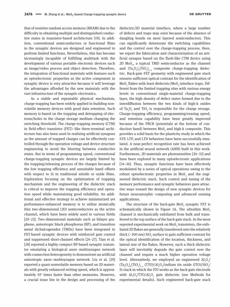
We first measured the current–voltage characteris-tics of the memory device. As shown in Figure 2A, n-type field-effect behaviors with clear on-state and off-state currents have been observed from the IDS–VBG transfer curves (IDS and VBG refer to the drain-source current and back-gate voltage, respectively). Large on/off current ratio greater than 105 has been achieved, which suggests that the interface traps introduced during the fabrication and flake transfer process are very limited as these positively charged traps can easily induce more electrons in the channel, decreasing the on/off ratio. The inset of Figure 2A shows the IDS–VDS (VDS: drain-source voltage) curves of the MoS2 CTM device with VDS swept from −1 to 1 V. The linear
VDS
Al2O3
VBGO
TTO
Si
ITO
Ti/Au
Ti/AuMoS2
SiO2
A
B C
Figure 1: Schematic and morphological structure of a MoS2 CTM device.(A) Schematic illustration of a MoS2 CTM device based on a back-gate FET structure. (B) Optical image of the MoS2 flake on surface of the dielectric stack with Ti/Au source/drain electrodes. The dotted line indicates the cut location in TEM test. (C) Cross-sectional TEM image of the device showing layers of 45-nm ITO, 15-nm Al2O3, 5-nm TTO, 4-nm Al2O3, and 2.9-nm MoS2. The image was obtained along the cut line shown in (C).
M. Zhang et al.: MoS2-based Charge-trapping synaptic device 2477
dependence of IDS on VDS indicates negligible contact resistance at the source/drain electrodes without signifi-cant charge injection barrier. This will enhance the drive capability of the device with higher on-state current.
A stable and sufficient memory window is a prereq-uisite for a memory device to obtain distinct and repeat-able multiple storage states as the basis for the synaptic functions in a neuromorphic system. Figure 2B shows the IDS–VBG hysteresis curves by sweeping VBG between −4 and 4 V. Clear clockwise hysteresis loops have been observed, suggesting the charge-trapping mechanism in the TTO layer. The memory is as large as 2 V, which is sufficient for effective multilevel storage applications. Such a high charge-trapping efficiency is ascribed to the high density of the trap states originated from the electron redistribu-tion between the cations with different valence and anion (oxygen) due to the appearance of the dangling bonds formed at the surface of each high-k oxide in the TTO layer [36]. Furthermore, by changing the VBG sweep range, the charge-trapped states in the device can be effectively tuned and modulated (Figure 2C).
The programming and erasing operations of the MoS2 CTM device can be understood through the band diagrams shown in Figure 3A and B, respectively. When
a positive VBG is applied, the electrons tunnel through the 4-nm-thick Al2O3 barrier following the conventional Fowler–Nordheim tunneling mechanism [37] and are trapped in TTO layer screening the back-gate electric field to reach the MoS2 channel. Such programming operation will result in a shift in the threshold voltage toward posi-tive direction (Figure 2D). When a negative VBG is applied, on the contrary, electrons are tunneling back from the TTO layer to the MoS2 channel, and holes tunnel through the Al2O3 barrier and are trapped in the TTO layer at the same time, leading to a threshold shifting to the negative direction (erasing operation in Figure 2E). The different memory states of the MoS2 device have been achieved by using both electrical and optical approaches. These results are in line with previous studies [33, 38]. The retention and endurance performance of the synaptic device are presented in Figure 3C and D. The device was programmed and erased by ±4-V gate voltage with 1-ms pulse width. The IDS current level was measured with 0.5 V VDS and −1 V VBG. Good charge retention characteristics have been observed, with only a small degradation in memory window after 104-s retention time, but the on/off ratio is still greater than 104. Such good retention is due to the intrinsic charge storage property of the TTO trapping
10–5
A B
D E
C1.5 × 10–6
1.0 × 10⁻⁶
5.0 × 10⁻⁷
0.0
I DS (
A)
VDS (V)
VDS (V)
0.20.4
VDS (V)
24
35
0.6
0.3
0.1
From –4 V to 4 V
From 4 V to –4 V
0.50.7
VDS (V)–2 –1
102
–5.0 × 10⁻⁷
–1.0 × 10⁻⁶
–1.5 × 10⁻⁶
–1.0 –0.5 0.0 0.5 1.0
10–6
10–7
10–8
I DS (
A)
I DS (
A)
I DS (
A)
I DS (
A)
10–9
10–10
10–11
10–5
10–4
10–6
10–7
10–8
10–9
10–10
10–11
I DS (
A)
10–5
10–6
10–7
10–8
10–9
10–10
10–11
–4 –2 0
VBG (V)
2 4–4 –2 0
VBG (V)
2 4
10–12
10–13–3 –2 –1 0
VBG (V)
VDS = 0.5 V
VBG (V)
1
10–6
10–7
10–8
10–9
10–10
10–6
10–5
10–7100 ns1 µs10 µs100 µs1 ms2 ms
100 ns1 µs10 µs100 µs1 ms2 ms
10–8
10–9
10–10
10–11
10–12
10–13
–3 –2 –1 0 1 2 3VBG (V)
–3 –2 –1 0 1 2 3
2 3
Figure 2: I–V characteristics of the MoS2 CTM device.(A) Transfer characteristics of the MoS2 transistor. IDS as a function of VBG with VDS varying from 0.1 to 0.7 V with 0.1-V step. Inset: IDS vs. VDS curves of the device with VDS swept from −1 to +1 V. (B) IDS–VBG hysteresis curves of the MoS2 CTM device under −4 V to +4 V VBG sweeping range showing sufficiently large memory window. (C) IDS–VBG hysteresis curves of the MoS2 CTM device in different VBG sweeping range of ±2, ±3, ±4, and ±5 V, respectively. (D) Programming operations on the MoS2 CTM device in different programming time at +4 V gate voltage pulse. (E) Erasing operations on the MoS2 CTM device in different erasing time at −4 V gate voltage pulse.
2478 M. Zhang et al.: MoS2-based Charge-trapping synaptic device
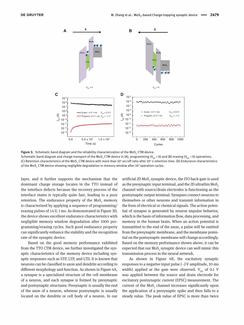
layer, and it further supports the mechanism that the dominant charge storage locates in the TTO instead of the interface defects because the recovery process of the interface states is typically quite fast, leading to a poor retention. The endurance property of the MoS2 memory is characterized by applying a sequence of programming/erasing pulses of ±4 V, 1 ms. As demonstrated in Figure 3D, the device shows excellent endurance characteristics with negligible memory window degradation after 1000 pro-gramming/erasing cycles. Such good endurance property can significantly enhance the stability and the recognition rate of the synaptic device.
Based on the good memory performance exhibited from the TTO CTM device, we further investigated the syn-aptic characteristics of the memory device including syn-aptic responses such as STP, LTP, and LTD. It is known that neurons can be classified to axon and dendrite according to different morphology and function. As shown in Figure 4A, a synapse is a specialized structure of the cell membrane of a neuron, and each synapse is formed by presynaptic and postsynaptic structures. Presynaptic is usually the end of the axon of a neuron, whereas postsynaptic is usually located on the dendrite or cell body of a neuron. In our
artificial 2D MoS2 synaptic device, the ITO back-gate is used as the presynaptic input terminal, and the 2D ultrathin MoS2 channel with source/drain electrodes is functioning as the postsynaptic output terminal. Synapses connect neurons to themselves or other neurons and transmit information in the form of electrical or chemical signals. The action poten-tial of synapse is generated by neuron impulse behavior, which is the basis of information flow, data processing, and memory in the human brain. When an action potential is transmitted to the end of the axon, a pulse will be emitted from the presynaptic membrane, and the membrane poten-tial on the postsynaptic membrane will change accordingly. Based on the memory performance shown above, it can be expected that our MoS2 synaptic device can well mimic this transmission process in the neural network.
As shown in Figure 4B, the excitatory synaptic responses to a negative input pulse (−2-V amplitude, 10-ms width) applied at the gate were observed. VDS of 0.1 V was applied between the source and drain electrode for excitatory postsynaptic current (EPSC) measurement. The current of the MoS2 channel increases significantly upon the application of a presynaptic spike and then falls to a steady value. The peak value of EPSC is more than twice
I DS (
A)
10–5
A B
C D
10–6
10–7
10–8Erase: –4 V 1 ms
Program: +4 V 1 ms
VDS = 0.5 V
VBG > 0 VBG < 0
VBG = –1 V
Erase: –4 V 1 ms
Program: +4 V 1 ms
VDS = 0.5 V
VBG = –1 V10–9
10–10
10–11
10–12
10–13
I DS (
A)
10–5
10–6
10–7
10–8
10–9
10–10
10–11
10–12
10–13
0 200 400
Cycles
600 800 10000.0 5.0 × 10² 1.0 × 10³
Time (s)
Figure 3: Schematic band diagram and the reliability characterization of the MoS2 CTM device.Schematic band diagram and charge transport of the MoS2 CTM device in (A), programming (VBG > 0) and (B) erasing (VBG < 0) operations. (C) Retention characteristics of the MoS2 CTM device with more than 104 on/off ratio after 104-s retention time. (D) Endurance characteristics of the MoS2 CTM device showing negligible degradation in memory window after 103 operation cycles.
M. Zhang et al.: MoS2-based Charge-trapping synaptic device 2479
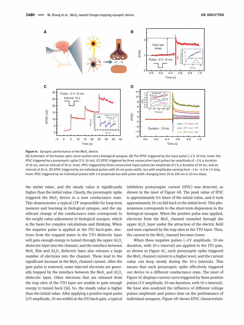
the initial value, and the steady value is significantly higher than the initial value. Clearly, the presynaptic spike triggered the MoS2 device to a new conductance state. This demonstrates a typical LTP responsible for long-term memory and learning in biological synapse, and the sig-nificant change of the conductance state corresponds to the weight value adjustment in biological synapse, which is the basis for complex calculations and thinking. When the negative pulse is applied at the ITO back-gate, elec-trons from the trapped states in the TTO dielectric layer will gain enough energy to tunnel through the upper Al2O3 dielectric layer into the channel, and the interface between MoS2 film and Al2O3 dielectric layer also releases a large number of electrons into the channel. These lead to the significant increase in the MoS2 channel current. After the gate pulse is removed, some injected electrons are gener-ally trapped by the interface between the MoS2 and Al2O3 dielectric layer. Other electrons that are released from the trap sites of the TTO layer are unable to gain enough energy to tunnel back [36]. So, the steady value is higher than the initial value. After applying a positive input pulse (2-V amplitude, 10-ms width) at the ITO back-gate, a typical
inhibitory postsynaptic current (IPSC) was detected, as shown in the inset of Figure 4B. The peak value of IPSC is approximately 0.4 times of the initial value, and it took approximately 20 s to fall back to the initial level. This phe-nomenon corresponds to the short-term depression in the biological synapse. When the positive pulse was applied, electrons from the MoS2 channel tunneled through the upper Al2O3 layer under the attraction of the electric field and were captured by the trap sites in the TTO layer. Thus, the current in the MoS2 channel becomes lower.
When three negative pulses (−2-V amplitude, 10-ms duration, with 10-s interval) are applied to the ITO gate, as shown in Figure 4C, each presynaptic spike triggered the MoS2 channel current to a higher level, and the current value can keep steady during the 10-s intervals. This means that each presynaptic spike effectively triggered our device to a different conductance state. The inset of Figure 4C displays current curve triggered by three positive pulses (1-V amplitude, 10-ms duration, with 10-s interval). We have also analyzed the influence of different voltage pulses amplitude and pulses time on the performance of individual synapses. Figure 4D shows EPSC characteristic
30
A B
C D12
10
8
6
4
2
0
–2Duration : 10 ms
EP
SC
EP
SC
(nA
)
IPS
C
1.2Pulse: –2 V, 10 ms
2
1EP
SC
00.0 0.2
Pulse: –2 V, 10 ms
Over twotimes
0.4
Time (s)
0.6 0.8 1.0
Pulse: –2 V, 10 ms
Interval: 10 s
Pulse: 1 V, 10 msInterval: 10 s
14131211109876–5 0 5 10 15 20
Time (s)
IPS
C (
nA)
25 30 35 40
Amplitude : 1 V20 ms
40 ms 60 ms
80 ms
100 ms
1.00.80.60.40.20.0
0 5 10Time (s)
IPS
C
1.2
1.01.1
0.90.80.70.60.50.4
0 10 20
Time (s)
–1 V
–3 V
–5 V
–2 V
–4 V
–6 V
15 20
–4
–6
25
20
15
10
5
0
–5 0 5 10 15 20
Time (s)
25 30 35 40 0.0 0.2 0.4
Time (s)
0.6 0.8 1.0
Figure 4: Synaptic performance of the MoS2 device.(A) Schematic of the human optic nerve system and a biological synapse. (B) The EPSC triggered by the input pulse (−2 V, 10 ms). Inset: the IPSC triggered by a presynaptic spike (2 V, 10 ms). (C) EPSC triggered by three consecutive input pulses (an amplitude of −2 V, a duration of 10 ms, and an interval of 10 s). Inset: IPSC triggered by three consecutive input pulses (an amplitude of 1 V, a duration of 10 ms, and an interval of 10 s). (D) EPSC triggered by six individual pulses with 10-ms pulse width, but with amplitudes varying from −1 to −6 V in 1 V step. Inset: IPSC triggered by six individual pulses with 1-V amplitude but with pulse width changing from 20 to 100 ms in 20-ms steps.
2480 M. Zhang et al.: MoS2-based Charge-trapping synaptic device
responses to different stimulus of six individual pulses with 10-ms width but with the amplitudes varying from −1 to −6 V in 1-V step. Note that the MoS2 FET was always restored to its initial condition before applying the pulse sequence of a particular amplitude. This is to make a fair and error-free comparison between the changes in the channel current as a function of pulse amplitude. As a higher gate voltage pulse would trigger more electrons to release from the TTO charge-trapping layer and tunnel into the channel, a larger voltage amplitude will trigger a higher current level. This is consistent with the results shown in Figure 4D. After applying a −6-V gate voltage pulse, the ratio between the maximum current value and the initial value can reach up to 1200%. This is due to the engineered back-gate stack with much thinner gate dielectric enhancing the gate control even under a small voltage level. The inset of Figure 4D shows IPSC charac-teristic curves when applying six individual pulses with 1-V amplitude but with pulse width changing from 20 to 100 ms in 20-ms steps. It is clear that the IPSC changes greater with the increase of pulse width.
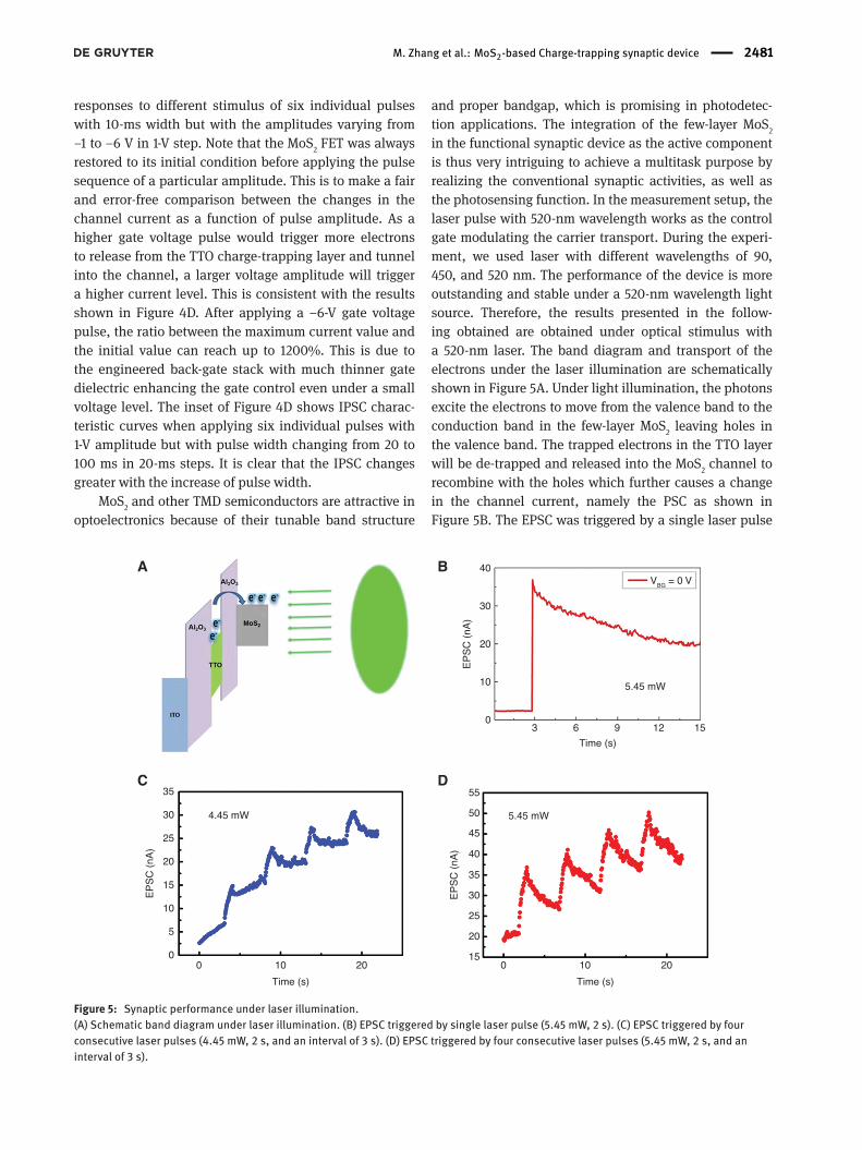
MoS2 and other TMD semiconductors are attractive in optoelectronics because of their tunable band structure
and proper bandgap, which is promising in photodetec-tion applications. The integration of the few-layer MoS2 in the functional synaptic device as the active component is thus very intriguing to achieve a multitask purpose by realizing the conventional synaptic activities, as well as the photosensing function. In the measurement setup, the laser pulse with 520-nm wavelength works as the control gate modulating the carrier transport. During the experi-ment, we used laser with different wavelengths of 90, 450, and 520 nm. The performance of the device is more outstanding and stable under a 520-nm wavelength light source. Therefore, the results presented in the follow-ing obtained are obtained under optical stimulus with a 520-nm laser. The band diagram and transport of the electrons under the laser illumination are schematically shown in Figure 5A. Under light illumination, the photons excite the electrons to move from the valence band to the conduction band in the few-layer MoS2 leaving holes in the valence band. The trapped electrons in the TTO layer will be de-trapped and released into the MoS2 channel to recombine with the holes which further causes a change in the channel current, namely the PSC as shown in Figure 5B. The EPSC was triggered by a single laser pulse
40A B
C D
30
20
EP
SC
(nA
)
10
0
55
5.45 mW50
45
40
35
EP
SC
(nA
)
30
25
20
150 10
Time (s)
2000
5
10
15
EP
SC
(nA
)
20
25
30
35
4.45 mW
10
Time (s)
20
3 6
Time (s)
9
5.45 mW
VBG = 0 V
12 15
Figure 5: Synaptic performance under laser illumination.(A) Schematic band diagram under laser illumination. (B) EPSC triggered by single laser pulse (5.45 mW, 2 s). (C) EPSC triggered by four consecutive laser pulses (4.45 mW, 2 s, and an interval of 3 s). (D) EPSC triggered by four consecutive laser pulses (5.45 mW, 2 s, and an interval of 3 s).
M. Zhang et al.: MoS2-based Charge-trapping synaptic device 2481
with 2-s width and 5.45-mW power intensity. Similar to the performance obtained by electrical gating, continu-ous EPSC can be observed when applying consecutive laser pulses, as shown in Figure 5C and D. Each laser pulse triggered the MoS2 channel current to a different level, and laser illumination with higher power intensity will trigger higher current. Table 1 lists and compares the typical performance of the recently reported TMD-based CTM devices and synapses incorporating high-k dielectrics or organics such as perylene-3,4,9,10-tetracarboxylic dian-hydride (PTCDA) and Poly(3,4-ethylenedioxythiophene)-poly(styrenesulfonate) (PEDOT:PSS). Such photosensing capability and the optical modulation over the conduction states in the channel have paved a solid pathway for syn-aptic functions such as visual processing in future multi-functional neuromorphic systems.
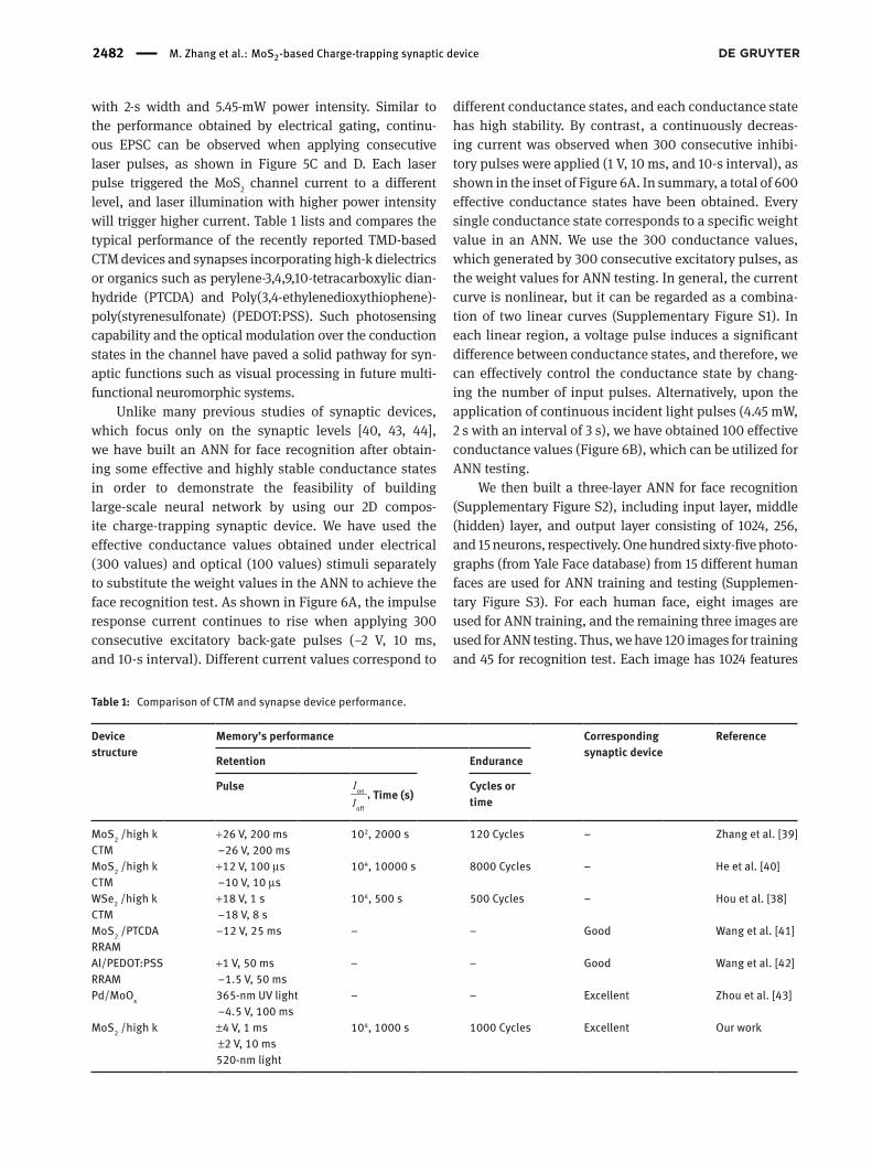
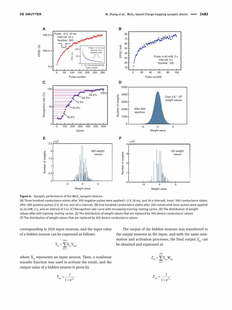
Unlike many previous studies of synaptic devices, which focus only on the synaptic levels [40, 43, 44], we have built an ANN for face recognition after obtain-ing some effective and highly stable conductance states in order to demonstrate the feasibility of building large-scale neural network by using our 2D compos-ite charge- trapping synaptic device. We have used the effective conductance values obtained under electrical (300 values) and optical (100 values) stimuli separately to substitute the weight values in the ANN to achieve the face recognition test. As shown in Figure 6A, the impulse response current continues to rise when applying 300 consecutive excitatory back-gate pulses (−2 V, 10 ms, and 10-s interval). Different current values correspond to
different conductance states, and each conductance state has high stability. By contrast, a continuously decreas-ing current was observed when 300 consecutive inhibi-tory pulses were applied (1 V, 10 ms, and 10-s interval), as shown in the inset of Figure 6A. In summary, a total of 600 effective conductance states have been obtained. Every single conductance state corresponds to a specific weight value in an ANN. We use the 300 conductance values, which generated by 300 consecutive excitatory pulses, as the weight values for ANN testing. In general, the current curve is nonlinear, but it can be regarded as a combina-tion of two linear curves (Supplementary Figure S1). In each linear region, a voltage pulse induces a significant difference between conductance states, and therefore, we can effectively control the conductance state by chang-ing the number of input pulses. Alternatively, upon the application of continuous incident light pulses (4.45 mW, 2 s with an interval of 3 s), we have obtained 100 effective conductance values (Figure 6B), which can be utilized for ANN testing.
We then built a three-layer ANN for face recognition (Supplementary Figure S2), including input layer, middle (hidden) layer, and output layer consisting of 1024, 256, and 15 neurons, respectively. One hundred sixty-five photo-graphs (from Yale Face database) from 15 different human faces are used for ANN training and testing (Supplemen-tary Figure S3). For each human face, eight images are used for ANN training, and the remaining three images are used for ANN testing. Thus, we have 120 images for training and 45 for recognition test. Each image has 1024 features
Table 1: Comparison of CTM and synapse device performance.
Device structure
Memory’s performance
Corresponding synaptic device
Reference
Retention
Endurance
Pulse II
on
off
, Time (s)Cycles or time
MoS2 /high kCTM
+26 V, 200 ms −26 V, 200 ms
102, 2000 s 120 Cycles – Zhang et al. [39]
MoS2 /high kCTM
+12 V, 100 μs −10 V, 10 μs
104, 10000 s 8000 Cycles – He et al. [40]
WSe2 /high kCTM
+18 V, 1 s −18 V, 8 s
104, 500 s 500 Cycles – Hou et al. [38]
MoS2 /PTCDARRAM
−12 V, 25 ms – – Good Wang et al. [41]
Al/PEDOT:PSSRRAM
+1 V, 50 ms −1.5 V, 50 ms
– – Good Wang et al. [42]
Pd/MoOx 365-nm UV light −4.5 V, 100 ms
– – Excellent Zhou et al. [43]
MoS2 /high k ±4 V, 1 ms ±2 V, 10 ms520-nm light
104, 1000 s 1000 Cycles Excellent Our work
2482 M. Zhang et al.: MoS2-based Charge-trapping synaptic device
corresponding to 1024 input neurons, and the input value of a hidden neuron can be expressed as follows:
1024
in m mnm 1
Y X V=
= ∑
where Xm represents an input neuron. Then, a nonlinear transfer function was used to activate the result, and the output value of a hidden neuron is given by
inon Y1Y
1 e=
+
The output of the hidden neurons was transferred to the output neurons as the input, and with the same sum-mation and activation processes, the final output Zok can be obtained and expressed as
256
ik on nkn 1
Z Y W=
= ∑
ikok1
1 ZZe
=+
400.0 n
A B
C D
E F
200.0 n
80
70
60
50
40
30
20
10
0 20 40 60 80 100
0.0
1005000
4000
3000
Num
ber
of w
eigh
ts
After 600epoches
Over 2.6 * 105
weight values
2000
1000
0–5 0
Weight value5
53.4%
73.3%
82.2%95.6%
100%
35.6%
50
Rec
ogni
tion
rate
(%
)
00 100 200 300
Epoch
2.5
300 weight values
100 weight values
×104 ×104
2
1.5
Num
ber
of w
eigh
ts
1
0.5
0–5 0
Weight value
5 –5 0
Weight value
5
4
3
Num
ber
of w
eigh
ts
2
1
0
400 500 600
0 50 100
Pulse number Pulse number
150 200 250 300
00
100 n
IPS
C (
A)
EP
SC
(A
)
EP
SC
(nA
)
200 nPulse: 1 V, 10 ms
Interval: 10 sNumber: 300
Pulse: –2 V, 10 msInterval: 10 sNumber: 300
Pulse: 4.45 mW, 2 sInterval: 3 s
Number: 10050 100
Pulse number150200250300
Figure 6: Synaptic performance of the MoS2 synaptic devices.(A) Three hundred conductance states after 300 negative pulses were applied (−2 V, 10 ms, and 10-s interval). Inset: 300 conductance states after 300 positive pulses (1 V, 10 ms, and 10-s interval). (B) One hundred conductance states after 100 consecutive laser pulses were applied (4.45 mW, 2 s, and an interval of 3 s). (C) Recognition rate curve with increasing training–testing cycles. (D) The distribution of weight values after 600 training–testing cycles. (E) The distribution of weight values that are replaced by 300 device conductance values. (F) The distribution of weight values that are replaced by 100 device conductance values.
M. Zhang et al.: MoS2-based Charge-trapping synaptic device 2483
So far, we have completed the forward propagation of the neural network. In order to train the network, we need to calculate the output error and modify the weight value through back-propagation. Comparing the above-calculated output with the correct output, the total output error can be obtained, and it is expressed as
152
1
1E ( )2 k k
k
O Z=
= −∑
where Ok is the correct output value. Then, the weight value is updated based on the derivative of the error during the back-propagation process. After updating the weights, a new image is fed to the ANN, and the weight update process is repeated until all 120 images have been used for training. Next, we use the trained network to identify the remaining 45 images and cal-culate the recognition rate. Generally, the recognition rate of the first recognition is very low, and in our ANN with 256 hidden neurons, the first recognition rate is only 17.78%. The face recognition rate keeps rising as the ANN learning proceeds deeper (Figure 6C), and the recognition rate can reach up to near 100% after 550 training–testing cycles. This proves that our ANN has excellent learning and recognition ability com-pared to previously published face recognition works [42]. Figure 6D shows the distribution of weight values after 600 training cycles (iterations), in which our ANN can achieve a near 100% recognition rate. Obviously, the weight distribution is very concentrated, and the weights became more scattered after more cycles (Sup-plementary Figure S4). To better demonstrate that our MoS2 device is suitable to be applied to ANNs, all weight values in the ANN network were replaced by 300 device conductance values, the distribution of replaced weight values is represented in Figure 6E. Similarly, the 100 conductance states achieved by incident light pulses are also used to replace the weight values following the rules that the conductance values and the ANN weight values are normalized within the same interval and that each weight value is substituted by the closest conduct-ance value. The distribution of replaced weight values (light) is represented in Figure 6F. It can be clearly seen that the shape of the statistical graph is basically the same as that in Figure 6C. Then, the replaced weight values were used in ANN for testing, and the recognition rate perfectly reached 100%. So, our devices can be used to build large-scale neural networks that can be modu-lated by using both electrical and optical approaches. In the reported similar face recognition work [42], the highest recognition rate is approximately only 95%,
which proves the excellent electrical properties of our MoS2 synaptic device and the optimal ANN design.
In summary, by combining a CTM architecture and engineered dielectric stack, a high-performance MoS2-based artificial synapse device has been demonstrated. The device exhibited excellent and steady synaptic characteristics and perfect recognition in our ANN. The results indicated that the intriguing synapses based on 2D materials are very promising for large-scale neu-romorphic systems and future artificial intelligence applications.
MethodsBefore fabricating the device, a 200-nm SiO2/Si substrate was first cleaned. Then, a 45-nm ITO film was sputtered on the substrate followed by a rapid annealing process at 400°C for 10 s in N2 as the back-gate electrode. A 15-nm Al2O3 was then deposited by atomic layer deposition (ALD) with the precursors of trimethylaluminum and H2O at 200°C as a blocking layer. And a 5-nm Ta2O5–TiO2 (TTO) mixture film composed of Ta2O5 and TiO2 (1:1) was sput-tered by using Ta2O5 and TiO2 ceramic targets as a charge-trapped layer [17]. After that, another layer of 4-nm Al2O3 was deposited by ALD as the tunneling layer. The MoS2 flake was mechanically exfoliated from a bulk material and selected with the thickness ranging from three to six layers, which is confirmed by TEM with a thickness of 2.9 nm (approximately four layers) (shown in Figure 1C). The Ti/Au electrodes were patterned by electron-beam lithography and deposited by electron-beam evaporation with the thickness 10/70 nm. Finally, the fabrication ends with a lift-off process. Figure 1B shows an optical image of the MoS2 channel with the source and drain electrodes. The width and length of the MoS2 channel were 20 and 10 μm, respectively. In order to accurately demonstrate the thickness of all components in our device, we cut the device along the dotted line, shown in Figure 1B, and analyzed it by TEM. The TEM photograph shows the thick-ness of the MoS2 channel is approximately 2.9 nm, which indicates that the MoS2 flake is approximately four layers thick. And the thickness of the engineered Al2O3/ TTO/ Al2O3 stack is 4/5/15 nm.
Acknowledgment: This research was supported by the National Key Research and Development Program of China (grant no. 2018YFB2202800), the Shanghai Municipal Science and Technology Commission (18JC1410300), the National Natural Science Foundation of China (61904033, 61522404, 61704030, and 61974144, Funder Id: http://
2484 M. Zhang et al.: MoS2-based Charge-trapping synaptic device
dx.doi.org/10.13039/501100001809), the Shanghai Rising-Star Program (19QA1400600, Funder Id: http://dx.doi.org/10.13039/501100013105), and the Basic Research Project of Shanghai Science and Technology Innovation Action (grant no. 17JC1400300).
References[1] LeCun Y, Bengio Y, Hinton G. Deep learning. Nature
2015;521:436–44.[2] Angermueller C, Pärnamaa T, Parts L, et al. Deep learning for
computational biology. Mol Syst Biol 2016;12:878.[3] Biamonte J, Wittek P, Pancotti N, et al. Quantum machine learn-
ing. Nature 2017;549:195–202.[4] Wunderlich T, Kungl AF, Müller E, et al. Demonstrating
advantages of neuromorphic computation: a pilot study. Front Neurosci 2019;13:260.
[5] Bokor J, Nádai L, Rudas IJ. Controllability of quantum bits from the von Neumann architecture to quantum computing. 2007 International Symposium on Computational Intelligence and Intelligent Informatics. 2007:9–12.
[6] Hinton G, Deng L, Yu D, et al. Deep neural networks for acoustic modeling in speech recognition: the shared views of four research groups. Agadir, Morocco, IEEE Signal Proc Mag 2012;29:82–97.
[7] Gokmen T, Vlasov Y. Acceleration of deep neural network train-ing with resistive cross-point devices: design considerations. Front Neurosci 2016;10:333.
[8] Cole MW, Bassett DS, Power JD, et al. Intrinsic and task-evoked network architectures of the human brain. Neuron 2014;83:238–51.
[9] Machens CK. Building the human brain. Science 2012;338:1156.
[10] Cotman CW, Nieto Sampedro M. Cell biology of synaptic plas-ticity. Science 1984;225:1287.
[11] Fuller EJ, Keene ST, Melianas A, et al. Parallel programming of an ionic floating-gate memory array for scalable neuromorphic computing. Science 2019;364:570–4.
[12] Suri DM, Querlioz D, Bichler O, et al. Bio-inspired stochastic computing using binary CBRAM synapses. IEEE T Electron Dev 2013;60:2402–9.
[13] Kund M, Beitel G, Pinnow C-U, et al. Conductive bridging RAM (CBRAM): an emerging non-volatile memory technology scal-able to sub 20nm. IEEE International Electron Devices Meeting, 2005. IEDM Technical Digest 2005;754–7.
[14] Kozicki MN, Barnaby HJ. Conductive bridging random access memory—materials, devices and applications. Semicond Sci Tech 2016;31:113001.
[15] Tsuruoka T, Terabe K, Hasegawa T, et al. Forming and switch-ing mechanisms of a cation-migration–based oxide resistive memory. Nanotechnology 2010;21:425205.
[16] Zhang SR, Zhou L, Mao JY, et al. Artificial synapse emulated by charge trapping-based resistive switching device. Adv Mater Technol 2019;4:1800342.
[17] Neale R, Nelson D, Moore GE. Nonvolatile and reprogram-mable, the read-mostly memory is here. Electronics 1970;43:56–60.
[18] Suri M, Bichler O, Querlioz D, et al. Phase change memory as synapse for ultra-dense neuromorphic systems: applica-tion to complex visual pattern extraction. Washington, DC, USA, Electron Devices Meeting (IEDM) 2011 IEEE International 2011;4.4.1–4.4.4.
[19] Park S, Noh J, Choo ML, et al. Nanoscale RRAM-based synaptic electronics: toward a neuromorphic computing device. Nano-technology 2013;24:384009
[20] Xing C, Xie Z, Liang Z, et al. 2D nonlayered selenium nanosheets: facile synthesis, photoluminescence, and ultra-fast photonics. Adv Opt Mater 2017;5:1700884–94.
[21] Xie Z, Wang D, Fan T, et al. Black phosphorus analogue tin sulfide nanosheets: synthesis and application as near-infrared photothermal agents and drug delivery platforms for cancer therapy. J Mater Chem B 2018;6:4747–55.
[22] Xie Z, Chen S, Duo Y, et al. Biocompatible two-dimensional titanium nanosheets for multimodal imaging-guided cancer theranostics. ACS Appl Mater Inter 2019;11:22129–40.
[23] Xie Z, Peng YP, Yu L, et al. Solar-inspired water purification based on emerging 2D materials: status and challenges. Solar RRL 2020;e1900400.
[24] Fan T, Zhou Y, Qiu M, et al. Black phosphorus: A novel nanoplat-form with potential in the field of bio-photonic nanomedicine. J Innov Opt Heal Sci 2018;11:1830003.
[25] Luo M, Fan T, Zhou Y, et al. 2D black phosphorus–based bio-medical applications. Adv Funct Mater 2019;29:1808306.
[26] Zhang B, Fan T, Xie N, et al. Versatile applications of metal sin-gle-atom@ 2D material nanoplatforms. Adv Sci 2019;6:1901787.
[27] Ahmed T, Kuriakose S, Mayes EL, et al. Optically stimulated artificial synapse based on layered black phosphorus. Small 2019;15:1900966.
[28] Tian H, Guo Q, Xie Y, et al. Anisotropic black phosphorus synaptic device for neuromorphic applications. Adv Mater 2016;28:4991–7.
[29] Liu C, Yan X, Song X, et al. A semi-floating gate memory based on van der Waals heterostructures for quasi–non-volatile appli-cations. Nat Nanotechnol 2018;13:404–10.
[30] Huang W, Xie Z, Fan T, et al. Black-phosphorus-analogue tin monosulfide: an emerging optoelectronic two-dimensional material for high-performance photodetection with improved stability under ambient/harsh conditions. J Mater Chem C 2018;6:9582–93.
[31] Fan T, Xie Z, Huang W, et al. Two-dimensional non-layered selenium nanoflakes: facile fabrications and applica-tions for self-powered photo-detector. Nanotechnology 2019;30:114002.
[32] Xing C, Huang W, Xie Z, et al. Ultrasmall bismuth quantum dots: facile liquid-phase exfoliation, characterization, and applica-tion in high-performance UV-Vis photodetector. ACS Photonics 2018;5:621–9.
[33] Gong F, Luo W, Wang J, et al. High-sensitivity floating-gate phototransistors based on WS2 and MoS2. Adv Funct Mater 2016;26:6084–90.
[34] Xie Z, Xing C, Huang W, et al. Ultrathin 2D nonlayered tellurium nanosheets: facile liquid-phase exfoliation, characterization, and photoresponse with high performance and enhanced stability. Adv Funct Mater 2018;28:1705833.
[35] Xie Z, Zhang F, Liang Z, et al. Revealing of the ultrafast third-order nonlinear optical response and enabled photonic application in two-dimensional tin sulfide. Photonics Res 2019;7:494–502.
M. Zhang et al.: MoS2-based Charge-trapping synaptic device 2485

[36] Wei C, Shen B, Ding P, et al. Ta2O5–TiO2 composite charge-trap-ping dielectric for the application of the nonvolatile memory. Sci Rep 2017;7:5988–8.
[37] Lenzlinger M, Snow EH. Fowler–Nordheim tunneling into ther-mally grown SiO2. J Appl Phys 1969;40:278–83.
[38] Hou X, Zhang H, Liu C, et al. Charge-trap memory based on hybrid 0D quantum dot-2D WSe2 structure. Small 2018;14:1800319.
[39] Zhang E, Wang W, Zhang C, et al. Tunable charge-trap memory based on few-layer MoS2. ACS Nano 2015;9:612–9.
[40] He L, Zhu H, Xu J, et al. Light-erasable embedded charge- trapping memory based on MoS2 for system-on-panel applica-tions. Appl Phys Lett 2017;111:223104.
[41] Wang S, Chen C, Yu Z, et al. A MoS2 /PTCDA hybrid heterojunc-tion synapse with efficient photoelectric dual modulation and versatility. Adv Mater 2019;31:1806227.
[42] Wang T, He Z, Liu H, et al. Flexible electronic synapses for face recognition application with multimodulated conductance states. ACS Appl Mater Inter 2018;10:37345–52.
[43] Zhou F, Zhou Z, Chen J, et al. Optoelectronic resistive random access memory for neuromorphic vision sensors. Nat Nano-technol 2019;14:776–82.
Supplementary Material: The online version of this article offers supplementary material (https://doi.org/10.1515/nanoph-2019-0548).
2486 M. Zhang et al.: MoS2-based Charge-trapping synaptic device