Baseband Hardware Designs in Modernised GNSS Receivers
22
1. Introduction The Global Positioning System (GPS) receiver has come a long way from being a specialised tool to a more general purpose everyday use mainstream gadget. This transformation is not only due to the advancements in semiconductor technology and embedded systems but also due to a highly concentrated research effort in the past decade that targeted a high performance, low power and affordable GPS receiver design. Before the ideas for such an efficient GPS receiver design could attain the saturation stage, the GPS modernisation and the development of several satellite navigation systems under the broader “Global Navigation Satellite Systems” (GNSS) umbrella, have brought a new dimension to the problem of efficient GNSS receiver design. The baseband signal processing engine forms an integral part of any GNSS receiver and is a key contributor to the overall cost and power consumption. This chapter discusses the challenges involved in designing baseband signal processing algorithms for a modernised GNSS receiver. The modernised GNSS receiver in this context includes processing elements not only for the GPS civilian signals GPS L1C/A, GPS L2C, GPS L5 and GPS L1C, but also for the Open Service (OS) signals from other satellite navigation systems that share the same frequency band as that of GPS. The Galileo satellite navigation system is one such example with its E1 and E5 OS signals sharing the GPS L1 and L5 (partial) frequency bands respectively. Though the underlying concept used in all these signals is “spread spectrum”, the structure of these signals differ due to different modulation techniques and signal parameters such as chipping rate, spreading code length, signal bandwidth and navigation data rate. These differences make the efficient baseband hardware design an interesting and useful research topic. The key objectives of this chapter are: 1. To revisit the existing efficient GPS L1 C/A baseband hardware methodologies and list best practices / learnings, 2. To analyse the complexity of the modernised GNSS baseband hardware and to identify key contributors to this complexity, 3. To explore design alternatives that deal with the key complexity contributors and to analyse the implementation feasibility of these design alternatives, 4. To ascertain the practicality of incorporating the design alternatives by implementing them on a FPGA based hardware platform, and Baseband Hardware Designs in Modernised GNSS Receivers Nagaraj C. Shivaramaiah and Andrew G. Dempster The University of New South Wales Australia 2 www.intechopen.com
Transcript of Baseband Hardware Designs in Modernised GNSS Receivers

1. Introduction
The Global Positioning System (GPS) receiver has come a long way from being a specialised
tool to a more general purpose everyday use mainstream gadget. This transformation is
not only due to the advancements in semiconductor technology and embedded systems but
also due to a highly concentrated research effort in the past decade that targeted a high
performance, low power and affordable GPS receiver design. Before the ideas for such an
efficient GPS receiver design could attain the saturation stage, the GPS modernisation and the
development of several satellite navigation systems under the broader “Global Navigation
Satellite Systems” (GNSS) umbrella, have brought a new dimension to the problem of efficient
GNSS receiver design. The baseband signal processing engine forms an integral part of any
GNSS receiver and is a key contributor to the overall cost and power consumption.
This chapter discusses the challenges involved in designing baseband signal processing
algorithms for a modernised GNSS receiver. The modernised GNSS receiver in this context
includes processing elements not only for the GPS civilian signals GPS L1C/A, GPS L2C, GPS
L5 and GPS L1C, but also for the Open Service (OS) signals from other satellite navigation
systems that share the same frequency band as that of GPS. The Galileo satellite navigation
system is one such example with its E1 and E5 OS signals sharing the GPS L1 and L5 (partial)
frequency bands respectively. Though the underlying concept used in all these signals is
“spread spectrum”, the structure of these signals differ due to different modulation techniques
and signal parameters such as chipping rate, spreading code length, signal bandwidth and
navigation data rate. These differences make the efficient baseband hardware design an
interesting and useful research topic.
The key objectives of this chapter are:
1. To revisit the existing efficient GPS L1 C/A baseband hardware methodologies and list
best practices / learnings,
2. To analyse the complexity of the modernised GNSS baseband hardware and to identify
key contributors to this complexity,
3. To explore design alternatives that deal with the key complexity contributors and to
analyse the implementation feasibility of these design alternatives,
4. To ascertain the practicality of incorporating the design alternatives by implementing them
on a FPGA based hardware platform, and
Baseband Hardware Designs in Modernised GNSS Receivers
Nagaraj C. Shivaramaiah and Andrew G. Dempster The University of New South Wales
Australia
2
www.intechopen.com

2 Will-be-set-by-IN-TECH
RF Front end
(Down-
converter +
ADC)
Digital
Baseband
(Correlator)
Processing
(Software)
Antenna
PVT
Solution
Fig. 1. Typical architecture of a GNSS receiver
5. To provide recommendations and guidelines for the design of a low power, high
performance, affordable multi-GNSS baseband hardware.
This chapter substantially draws on one of the authors’ conference papers published in ISCAS
2010 (Shivaramaiah & Dempster, 2010).
2. GNSS receiver and baseband hardware
2.1 GNSS receiver architecture
Fig. 1 shows the typical architecture of a GNSS receiver. Each signal from a different frequency
band is down-converted and passed through an Analog-to-Digital-Converter (ADC) to obtain
the Intermediate Frequency (IF) samples. The baseband signal processing hardware (widely
known as the correlator) is usually implemented in hardware. With the help of feedback
control algorithms (implemented either as a part of the digital hardware or as a part of
the processing in software), the baseband circuit provides accurate estimates of the delay,
phase and frequency of the carrier and spreading code in the received signal (tracking). The
baseband circuit is also used for the initial coarse estimates of these parameters (acquisition).
The processing, usually implemented in software, computes the Position-Velocity-Time (PVT)
solution (Braasch & van Dierendonck, 1999; Kaplan & Hegarty, 2006; Parkinson & Spilker,
1995).
2.2 Generic baseband architecture for the tracking process in a GNSS receiver
This section describes a generic architecture for the GNSS baseband that allows the basic
functionality of tracking the signal. Though the same architecture can be used for the signal
acquisition process, the signal acquisition is not the focus here. The GNSS baseband hardware
in its usual definition is comprised of all the signal processing circuits bounded on the input
side by the sampled and digitised IF signal, and on the output side by the received signal
measurements (carrier phase, code phase, navigation data bits, signal strength, etc.). Fig.
2 shows the functional diagram of generic GNSS baseband hardware for a single signal
component. The functionality of each block is described in detail elsewhere in the literature
(e.g. Kaplan & Hegarty (2006)) and will be discussed briefly here.
The baseband functionality can be broadly divided into two parts.
1. Core Correlator Hardware
The core hardware is responsible for correlating the input signal with the local replica and
producing the correlation values.
34 Global Navigation Satellite Systems – Signal, Theory and Applications
www.intechopen.com

Baseband Hardware Designs in Modernised GNSS Receivers 3
Carrier
Mixer
Local
Reference
Mixers
Carrier
Generator
Carrier
NCOCode NCO
Code
Generator
Sub-carrier
Generator
Subcarrier
NCO
Subcarrier
Modulator
Shift
Register
... R1
...
1
2R
Nacc -bit
Accumulators
...
1
2R
Decision and
Feedback
ControlMeasurements
Convolution
Decoder
Navigation
data
Timing
Control (to
all
sequential
blocks)
CLK
Nif
Ncar
N1
Nref
N2
Nref
Nacc
Nnco1
Nnco2
Nnco3
Local signal generation and control
IF samples
Correlation computation
Fig. 2. A functional diagram of the baseband hardware (thick lines carry N• bits, dashedboxes are optional )
2. Correlator Controller
The controller processes the correlation values produced by the core hardware and makes
decisions based on a set of feedback control algorithms. The threshold detection during the
acquisition, the carrier and code locked loops during the tracking, the process of dictating
the parameters for the local replica carrier and replica code generation, are all included in
this part.
The core correlator hardware functionality can again be divided into two parts.
1. Correlation Computation
2. Local Signal Generation
The necessity of this second level functionality division is due to the new signals that will
be dealt with in future sections. This type of segregation of the core correlator hardware
functionality helps accommodate new signals both at the same frequency that may belong to
a different constellation and the signals at different frequency bands of the same constellation.
The input to the baseband hardware is the sampled and digitized IF signal with Ni f -bit
quantization at a sampling frequency of fs Hz. In order to demodulate the navigation data
bits, the baseband module must first remove the carrier and the spreading code from the signal
(Braasch & van Dierendonck, 1999).
The IF samples are mixed with the locally generated carrier in the carrier mixer. The local
carrier frequency generator aims to match the frequency of the input signal. Both in phase
35Baseband Hardware Designs in Modernised GNSS Receivers
www.intechopen.com

4 Will-be-set-by-IN-TECH
and quadrature phase signals are generated with Ncar-bit quantization. The carrier mixer
output results in N1-bit values.
The local replica code+subcarrier signal, referred to here as the local "reference signal" is
Nre f -bit wide. In the absence of the subcarrier, Nre f =1 because the spreading code takes only
the values of 1 or 0. Since most of the signal tracking algorithms employed in a GNSS receiver
use the delay tracking principle, delayed versions of the local reference signal are generated
with the help of shift registers. R is the number of local reference signal “arms” (sometimes
referred to as "taps" or "fingers"), typically three: the Early, the Prompt and the Late).
The local reference mixer generates 2R values each N2-bits wide as a result of combining
in phase and quadrature values with the local reference signal. These individual sample
correlation values are accumulated in a Nacc-bit accumulator for a predefined “integration
duration”. The tracking loops act on these accumulator outputs and adjust the local carrier
frequency and the code delay so as to maintain lock (to be at the peak of the correlation
function). The tracking loops also produce the measurements and also demodulate the
navigation data bits present in the signal (Shivaramaiah, 2004).
2.3 Bit-width requirements of the correlator components
The parameters of interest for the complexity analysis of the core correlator are the number
of bits required to represent the intermediate signals, the bit-width of the accumulator and
other registers and the minimum frequency of operation required for a particular signal (or
any component of a signal thereof). The notations for the number of bits at different stages
are shown in Fig. 2, as N• along with the thick lines. In the following paragraphs a brief
description of each of the underlying modules is given and the number of bits required for
the accumulator is derived.
2.3.1 ADC/IF (Ni f )
The signal loss due to the quantisation beyond 2-bits is insignificant as long as the sampling
thresholds are sensibly set (Hegarty, 2009). However, 3-bits and more have been used to
alleviate the problems with the AGC in the presence of RF interference (Kaplan & Hegarty,
2006). Commercial mass-market receivers normally use 2-bit uniform sign-magnitude
quantisation with 4 levels {±1,±3}(Zarlink, 1999, 2001). Therefore for the examples in this
chapter it is safe to assume Ni f = 2.
2.3.2 Local carrier generator (Ncar)
The loss due to the local carrier quantisation is studied in Namgoong et al. (2000).
Typically, 3-bit uniform NCO phase quantisation and 2-bit amplitude quantisation with 4
levels {±1,±2} is used. More bits in the phase and amplitude quantisation increases the
Spurious-Free-Dynamic-Range (SFDR) and reduces the quantisation noise. However this has
a significant impact on the size of succeeding stages.
36 Global Navigation Satellite Systems – Signal, Theory and Applications
www.intechopen.com

Baseband Hardware Designs in Modernised GNSS Receivers 5
2.3.3 Carrier mixer (N1)
The carrier mixer basically multiplies the input signal with the local carrier bits. Since the
resulting values will only have 8 levels {±1,±2, ±3,±6}, a 3-bit encoding is sufficient.
Observe that with the 3-bit encoding, arithmetic operation cannot be directly performed.
Hence if the succeeding stage requires an arithmetic representation then four bits should be
used.
2.3.4 Subcarrier generator & subcarrier modulator (Nre f )
The local code takes on values of either 0 or 1 and hence 1-bit is sufficient for its representation.
However, the number of bits required to represent the subcarrier depends on the number of
levels in the subcarrier used for the modulation. BOC signals use a 2-level {±1} subcarrier
thus requiring only 1-bit for the representation. AltBOC uses 4-levels (dominant component
of the subcarrier) which require more bits for the representation and in such situations
approximation needs to be used to use smaller bit-width representations. The local spreading
code modifies only the sign of the subcarrier at the output of the subcarrier modulation.
Hence, Nre f will depend on the number of bits used for the subcarrier representation.
2.3.5 Local reference mixer (N2)
This can be easily determined from the number of levels of the two inputs. However, the
succeeding stage (the accumulator) is an arithmetic operation and requires binary two’s
complement representation. This leads to an additional bit at the output. For example, with
the 8-level N1 {±1,±2,±3,±6} and the 4-level Nre f {±1,±2}, the resultant set will have
only 12 levels {±1,±2,±3,±4,±6,±12}, but due to the later requirement of signed binary
representation the output must be 5-bit wide. Let the sample-maximum (magnitude) of the
output at this stage be denoted by A2.
2.3.6 Accumulator (Nacc)
The interval between two consecutive accumulator resets is generally determined by the
coherent integration duration and the coherent integration duration in turn in most cases will
be a multiple of the spreading code period. Let N′
acc denote the number of bits required to
represent the worst-case value at the output of the accumulator. Then
N′
acc =
⌈
log−12
(
A2
⌊
fs
fcoMcL
⌋)
+ C + 1
⌉
(1)
where fs ∈ R+ is the sampling frequency in Hz, fco ∈ R+ is the chipping rate (with
any associated Doppler frequency) in Hz, L ∈ N is the primary code length, Mc ∈ Q is
the number (or fraction) of primary code periods in the coherent integration and C is the
complex modulation indicator, C ∈ {0 = Normal, 1 = Complex}. (1) clearly satisfies the
Design-For-Test (DFT) guidelines, but it is an overkill as all the samples may not end up with
a value of A2. In reality the sample-maximum is controlled by the input signal strength and
the local carrier frequency. Hence the required accumulator width Nacc < N′
acc.
37Baseband Hardware Designs in Modernised GNSS Receivers
www.intechopen.com

6 Will-be-set-by-IN-TECH
An R-arm correlator will have 2R(C + 1) accumulators (due to the in-phase and quadrature
carrier components) and hence accumulator width plays a very important role in correlator
complexity. Some correlators use re-sampling prior to the local reference mixer stage (e.g.
(Namgoong et al., 2000)), to reduce the number of samples input to the accumulator. However
those special techniques are outside the scope of the discussion here.
2.4 Efficient realisation of the correlator core for the GPS L1 C/A signal
As mentioned in the previous section, the input to the correlator is the sampled IF signal.
Each sample in the sampled IF signal, when mixed with local carrier and the local reference
signal, produces a correlation value (“sample correlation value”) which is then fed to the
accumulator. Therefore, in the correlator core of Fig. 2, all the blocks do not require sequential
logic. The carrier mixer, subcarrier modulation and the local reference mixer are typically
implemented as combinational logic. Latching the input signal, carrier NCO, code NCO and
the accumulator are implemented as sequential logic. As a result, the combined propagation
delay of all the combination logic blocks should be less than the sampling period tpd + taccsu <
1/ fs, where tpd is the propagation delay and taccsu is the setup time of the accumulator.
The combinational block has to compute the sample correlation value from the three inputs
viz. the incoming signal, the local carrier and the local reference signal. The carrier mixer
and the local reference mixer can be realised using Look-Up-Tables (LUTs) separately or
together. For the single-bit reference signals, the circuit can be further simplified by feeding
the local code to select the add or subtract operation of the accumulator. Fig. 3(a) shows a
generic way to realise the correlation computation blocks’ combinational logic. The number
of instantiations of each block is mentioned above the block. Observe that two carrier mixer
blocks are required (I and Q), six reference signal mixer blocks are required (early, prompt and
late version of reference signals mixed with I and Q carrier mixer outputs) and six accumulator
blocks are required for the complete operation.
Fig. 3(b) shows a realisation of the combinational logic using the LUT method for the GPS
L1 C/A signal. In Fig. 3, the input signal and the local carrier are assumed to be 2-bit
wide and the local reference signal (in this case only the local code) is 1-bit wide. Observe
that the sample correlation output is represented using four bits even though there are only
eight possible values. This is because the succeeding stage (which is the signed addition, a
part of the accumulation process) is an arithmetic operation and hence the sample correlation
values need to be represented in 2’s complement format. The local code mixer is eliminated
by using the local code output as the Add/Sub selection input of the accumulator. The output
therefore consists of six correlation values: inphase-early, inphase-prompt, inphase-late,
quadrature-early, quadrature-prompt and quadrature-late. These correlation values are fed
to the tracking loops for further processing.
3. Impact of the signal structure on the core correlator architecture
This section analyses the impact of the change in certain parameters of the signal (due to the
structure of the new signals) on the architecture of the core correlator.
38 Global Navigation Satellite Systems – Signal, Theory and Applications
www.intechopen.com

Baseband Hardware Designs in Modernised GNSS Receivers 7
16x4 LUT
IF Signal
Local Carrier
Local Code
Sample
Correlation2
2
4
Accumulator
Add/Sub
Data
Correlation
value
16
Logic /
LUT
IF Signal
Local C
arr
ier
Sample
CorrelationAccumulator
Data
Correlation
valueLogic /
LUT
Local R
ef
sig
nal
Add/Sub
Data
x2 (I & Q)x6 (E,P,L
and I,Q)
x6 (E,P,L
and I,Q)
x2 (I & Q)x6 (E,P,L
and I,Q)
Clk
Clk
(a)
(b)
Fig. 3. Realisation of the correlation computation blocks (a) Generic implementation (b) animplementation for the GPS L1 C/A signal
3.1 Longer codes (or longer code period)
3.1.1 Shift register generated codes
Longer codes are usually obtained by wide shift registers or a combination of shift registers.
Typically the baseband circuit will have the same number of code generators as the number of
channels. If the baseband has to implement multiple tracking channels to simultaneously
process multiple signals then the additional number of bits in the shift register brings in
additional hardware which is not insignificant.
3.1.2 Memory codes
Memory codes eliminate the need for a code generator (i.e the shift registers and XOR gates
used for the code generation). However the codes for all the pseudo random noise (PRN)
sequences must be stored in a circular buffer or ROM. The decision on whether to use a circular
buffer or ROM depends on the overall architecture of the receiver. For tracking the signal, it is
enough to read the buffer sequentially (like in a FIFO) and no address generation is required.
However if there is a requirement to read the local code from a particular delay (which could
be the case when the receiver wants to reacquire the signal) then it is better to use the ROM
39Baseband Hardware Designs in Modernised GNSS Receivers
www.intechopen.com

8 Will-be-set-by-IN-TECH
which then demands a separate address generator. The read clock to the FIFO or the ROM is
nothing but the output of the code NCO.
Another issue with the memory codes is the way the codes are stored. The codes for all the
PRNs cannot be stored in a single memory because it will limit the access of the memory from
different channels. Hence the code for each PRN should be stored in a separate memory block.
Even in this situation, there is a constraint on the architecture. During the signal acquisition
or during the tracking if there is a requirement for more than one GNSS channel to use the
same PRN, then the memory block will have to have more than one port which is expensive
in terms of the resource and power consumption.
3.1.3 Effect on the accumulator bit-width
Another consequence of longer codes is that the number of bits in the accumulator has to
be increased, i.e. the Nacc requirement increases (assuming that the accumulator is used to
integrate the correlation values for the duration of one code period).
3.2 Subcarrier modulation
3.2.1 Two-level (1-bit) subcarriers
With the subcarrier modulation an additional NCO, subcarrier generator and subcarrier
modulator may be required depending on the requirement of the tracking loops. If the
subcarrier has only two levels then the subcarrier and the replica code bit can be combined
with the help of a single XOR gate and the result will also be a 1-bit value. This does not
change the other parts of the correlation computation circuit and also the reference signal can
still be fed to the Add/Sub input of the accumulator.
3.2.2 Multi-level (> 1-bit) subcarriers
If the subcarrier has multiple levels (i.e. requiring more than 1-bit) then the process of
combining the replica code bit and the subcarrier is not a simple XOR operation, but requires a
negation operation which results in the same number of bits as the subcarrier (Nre f ). Secondly,
the width of the shift register that generates the early, prompt and late values should be
increased to Nre f . Since the reference signal is not represented by a single bit it cannot be used
directly as an input to the accumulator and therefore there needs to be a dedicated reference
signal mixer block. Thirdly, the reference signal mixing operation should accommodate this
bit-width increase in one of the inputs. As a result, the number of bits required to represent
the sample correlation value will increase, which in turn increases the number of bits in the
accumulator.
3.3 Modulation type
The BOC family of signals has a narrow autocorrelation main peak. As a result the spacing
between the R delayed versions of the reference signals should be reduced in order to achieve
better tracking performance (Shivaramaiah & Dempster, 2009). Reduction in the spacing
requires the code and the subcarrier NCO to be operating at a higher clock frequency. This
constrains the minimum clock frequency requirement of these NCOs. As a result, the overall
40 Global Navigation Satellite Systems – Signal, Theory and Applications
www.intechopen.com

Baseband Hardware Designs in Modernised GNSS Receivers 9
operating frequency requirement of the correlator will go up and also an additional clock
divider circuit is required.
3.4 Multiple signal components
When a signal has more than one component (say pilot and data components), it is wise
to compute the correlation values independently for each signal component, thus allowing
the subsequent processing blocks to use efficient tracking techniques (Shivaramaiah, 2011).
One can optimise the correlation computation blocks by combining the logic for the signal
components but that would give a combined correlation value to the tracking loops. This
combined correlation value may suffer from loss due to the data and or code bit inversions
between the signal components. Therefore it is wise to isolate the different signal components
at the correlation computation stage (and combine in the succeeding stages if required).
3.5 Receiver bandwidth and the operating frequency
Receiver bandwidth has a direct impact on the sampling frequency and hence the operating
frequency of the circuit. While some baseband blocks can be fed a slower clock than the
sampling frequency (but still derived from the sampling frequency), some other blocks have
to operate at the sampling frequency itself. Any bandwidth reduction below the minimum
required (which is typically the bandwidth occupied by the main lobe(s)) done before the
correlation operation stage, will result in rounded auto-correlation peaks, which in turn result
in noisier range measurements. Therefore it is a good practice to keep the operating frequency
at least equal to the sampling frequency until the carrier mixing stage and at least equal to four
times the subcarrier frequency (or the twice the code frequency in the absence of subcarrier)
from the reference signal mixer stage onwards.
3.6 Complex modulation
In the case of AltBOC signals the lines generated within the core correlator portion in Fig. 2
carry complex signals. The local reference mixer LUT must cater for the complex correlation
operation.
There are basically two ways to realise this complex reference signal mixer: with the logic
or with LUTs. With the logic one would be using adders/subtracters and multipliers of
appropriate length to compute the reference signal mixer outputs. With the LUT, there are
many ways, each using different sizes of the LUT. In both the cases the resource requirement
would significantly increase compared to the GPS L1 C/A correlator (which requires no
reference signal mixer).
4. Core correlator architectural modifications for the new signals
4.1 New GNSS signals and general requirements
Table 1 revisits the centre frequency, typical receiver bandwidth and code lengths of some
of the new open service signals. These parameters largely determine the architecture and
complexity of the baseband signal processing stage in a GNSS receiver.
The following are the important points to note from the table.
41Baseband Hardware Designs in Modernised GNSS Receivers
www.intechopen.com

10 Will-be-set-by-IN-TECH
Signal name Centre frequency
(Typical receiver
bandwidth) in
MHz
Modulation
type
Code length *
(memory code?
Y/N)
Chipping rate
(MHz)
GPS L1 C/A 1575.42 (2) BPSK 1023 (N) 1.023
GPS L2C 1227.6 (2) BPSK CM-20460 (N),
CL-767250 (N)1.023
GPS L5 1176.45 (20) BPSK 20460 (N) 10.23
GPS L1C, Galileo
E1, Compass B1
1575.42 (14) MBOC / CBOC 1023 (N), 4096
(Y), **
1.023
Galileo E5,
Compass B2
1191.795 (50) AltBOC 10230 (N), *** 10.23
** Primary code only, *** Yet to be available for the Compass signal
Table 1. Some new GNSS signals and their parameters of interest
1. increased signal bandwidths demand higher sampling frequencies
2. increased spreading code lengths and chipping rates demand higher shift register clock
frequencies,
3. use of multi-level subcarriers, as in the case of AltBOC type of modulation, increases the
number of bits in the local reference signal,
4. use of memory codes demands additional memory to hold the spreading code for all the
satellites, and
5. increased minimum operating frequency of the baseband hardware mainly due to a) and
b)
The operating frequency and the circuit complexity determine the energy efficiency of digital
logic and therefore the design of an efficient baseband logic circuit becomes extremely
important in the context of baseband hardware targeted to process multi-GNSS signals
(Shivaramaiah et al., 2009).
This section discusses the major contributors for the resource utilisation of the correlators for
the new signals. The parameters of the correlator that processes GPS L1 C/A signal are used
as the reference.
4.2 GPS L2C
4.2.1 GPS L2C - CM
The L2C - CM code generation requires a 27-bit shift register instead of the 10-bit code
generator shift register that is used to generate the L1 C/A signal. This in turn increases the
code generator read /write and control register bit-widths. The operating frequency remains
the same and hence any increase in the power consumption is only due to the increase in the
number of shift register bits.
4.2.2 GPS L2C - CM and CL)
The additions to the L2C - CM only correlator are : another 27-bit shift register, another set
of code mixers and accumulators. Since the CM and CL codes are time-multiplexed, the
42 Global Navigation Satellite Systems – Signal, Theory and Applications
www.intechopen.com

Baseband Hardware Designs in Modernised GNSS Receivers 11
number of accumulators remains the same if the CM and CL correlation values are combined
(the spreading codes can be combined in time similar to what is done at the transmitter).
However, the combination will lead to data bit ambiguity problem (Dempster, 2006). When
the components are combined, the increase in the power consumption with respect to the
L2C- CM only signal case is negligible. If both the CM and the CL signal components are
processed independently then the resource utilisation almost doubles compared to the CM
only processing.
4.3 Galileo E1
4.3.1 Single signal component (E1b or E1c)
Because of the use of memory codes, the baseband can eliminate the shift register and store
the local spreading code in memory. Therefore there is a small saving in terms of the
flip-flops/registers compared to the GPS L1 C/A architecture. However, because of the 8
MHz sampling frequency requirement assumption, one expects to see an increase in the power
consumption.
4.3.2 Both the signal components (E1b and E1c)
Here two sets of memory codes are used each occupying 4092 bits. In addition the number
of local reference mixers and accumulators are not only doubled, but also need to operate at
higher frequencies due to the higher sampling frequency. For this reason the expected power
consumption is close to twice that of the single signal component (E1b or E1c).
4.4 GPS L5 (pilot and data)
For the GPS L5 signal, the code generator shift register requires 13 bits, which is not a
significant increase from the 10-bits of GPS L1 C/A. However, the major difference is the
higher chipping rate which demands a higher sampling frequency and in turn a higher
correlator operating frequency. Due to the longer code length, the accumulators also have
to be wide compared to that of the GPS L1 C/A correlator. As a result of the increased
operating frequency, the power consumption requirement is expected to drastically increase
though the resource utilisation would go up only slightly more than twice that of the GPS L1
C/A correlator.
4.5 Galileo E5
4.5.1 Galileo E5a or E5b (pilot and data)
For the Galileo E5a and E5b signals, the code generator shift register requires 14-bits. This
is only a 1-bit change from the case of GPS L5 correlator and hence all the other circuit
parameters (such as bit widths) will be very close to that of the GPS L5 correlator. Hence
the expected power consumption for E5a or E5b signal when processed individually, would
be close to that of the GPS L5 correlator.
43Baseband Hardware Designs in Modernised GNSS Receivers
www.intechopen.com

12 Will-be-set-by-IN-TECH
4.5.2 Galileo E5 wideband
In this case both the E5a and E5b signals are processed together as a single wideband signal
(with a bandwidth of at least 51.15 MHz). The local code has to be generated individually
for all the four components (E5a-pilot, E5a-data, E5b-pilot and E5b-data) of the signal and
the generators require 14-bit shift registers. However, because the four signal components
and the complex modulation, the local reference mixer is computationally intensive (more
LUTs). In addition, a quadruple number of accumulators are required. As mentioned earlier,
independent correlation for all the four signals is performed to allow design freedom for
the subsequent stages in combining these four components. As a result of a very high
operating frequency and drastic increase in the resource requirements compared to GPS L1
C/A correlator, the power consumption is expected to be very high.
4.6 Baseband architecture overview for the GPS and Galileo OS signals
Fig. 4 shows the baseband architecture assuming that the correlator processes GPA L1 C/A,
L2C, L5 and Galileo E1, E5 signals. The computation block is marked separately to the local
signal (local carrier and replica reference signal) generation block. This sort of grouping
the blocks helps the design because different signals (and different channels in some cases)
share common parameters and optimising the hardware becomes easier. In this architecture,
it is also assumed that the baseband is commanded (assigned PRNs, Doppler and delay
parameters etc) to operate from an external processor. The correlation values of different
signals are read and processed in the succeeding decision feedback and control stage.
5. Resource requirements for the new signals and recommendations
5.1 Core resource requirements using a straightforward extension of the GPS L1 C/A
design
In order to gauge the resource requirements in terms of the number of registers and
combinational logic, the core correlators for the GPS and Galileo open service signals have
been implemented on the Altera Cyclone-III family device EP3C120F780C8. The FPGA
resource utilisation parameters are listed in Table 2.
The resource and the power consumption values closely match the expected outcomes
mentioned in the previous section. While the Galileo E1b or E1c core requires almost the same
resources as that of GPS L1 C/A, the power consumption is higher. The power consumption
for the single component Galileo E1 is 0.8mW more than that of the GPS L1 C/A. This is due
to the presence of the memory block, increased accumulator width and increased operating
frequency. The Galileo E1 correlator where both the E1b and E1c signals are processed
together has a power estimate of 2.24mW, only about 0.6mW more than the single component.
This is because some of the blocks such as the carrier NCO and the carrier mixer are common
for both the signal components.
The resource for the GPS L5 signal is increased to 701 registers and 204 combinational units
which is due to the increase in the accumulator width and also due to the presence of two
signal components. The power consumption estimate of the GPS L5 signal is about 11 times
that of the GPS L1 C/A signal and is attributed mainly to the operating frequency. The
44 Global Navigation Satellite Systems – Signal, Theory and Applications
www.intechopen.com

Baseband Hardware Designs in Modernised GNSS Receivers 13
L1/E1 IF
Signal
L2C IF
Signal
L5/E5 IF
Signal
L1 core
E1 core
L2C core
L5 core
E5 core
Correlation computation
(x Number of channels)
Local signal
generation (for all
channels)
Mux
Mux /
Demux
and
Controller
Interface
Controller
Corr
ela
tion v
alu
es
Com
mand
and s
tatu
s
Code
memory
blocks (all
PRNs)
Fig. 4. Components of the baseband module for GPS L1/L2C/L5 and Galileo E1/E5 signals
Signal /
Component
Correlator
Operating
Frequency
(MHz)
Resource Utilisation Power
estimate
(mW)
Registers Combina-
tional
Memory
(bits)
GPS L1 C/A 4 446 151 - 1.06
Galileo E1b or E1c 8 436 149 4092 1.84
Galileo E1 (E1b and
E1c)
8 631 176 8184 2.24
GPS L2C CM only 4 478 210 - 1.13
GPS L2C (CM and
CL)
4 737 245 - 1.61
GPS L5 (Pilot and
Data)
40 701 204 - 11.93
Galileo E5a or E5b 40 694 203 - 11.80
Galileo E5 100 1010 253 - 39.28
Table 2. Resource utilisation and power consumption estimates of the core correlator (singlechannel) for different signals
45Baseband Hardware Designs in Modernised GNSS Receivers
www.intechopen.com

14 Will-be-set-by-IN-TECH
L2−CM L2 E1b E1 L5 E5a E50
5
10
15
20
25
30
35
40
Signal (Signal Component)
Po
we
r C
on
su
mp
tio
n (
ratio
w.r
.t.
GP
S L
1 C
/A)
1.07 1.52 1.74 2.11
11.25 11.13
37.06
Fig. 5. Ratio of the power estimate for new signals with respect to GPS L1 C/A
resource and power consumption of the Galileo E5a and E5b signals is close to that of the
GPS L5 correlator, as expected. As a result of a very high operating frequency the power
consumption of the wideband Galileo E5 correlator shoots up to almost 37 times that of the
GPS L1 C/A signal. The power consumption for the E5 signal can be reduced a little bit further
by focusing more on how the complex mixers are realised as discussed in Shivaramaiah (2011).
The ratio of the power consumption estimate with respect to the GPS L1 C/A is shown in
Fig.5. The power consumption was estimated using the PowerPlay Analyzer tool with real IF
signal samples provided as an input1 to the baseband module.
5.2 Complexity comparison results for different baseband configurations
Fig. 6 shows the power consumption of different signals vs. the number of
channels. A “channel” comprises the core correlator, timing control, address and data
multiplexer/demultiplexer (for a memory mapped interface to the subsequent stage), and
some housekeeping operations. Although the resource consumption is not described in detail
here, it should be mentioned that the two major memory spreading code sets in the case of
the Galileo signal occupy around 410K bits (E1, 4092 bits, 2 signal components, 50 PRNs) of
memory and 10K bits (E5 secondary code, 100 bits, 2 components, 50 satellites) which are
totally new additions to the GNSS receiver baseband hardware.
1 The PowerPlay tool estimates the toggle rate of the internal nets and the output pins based on the inputsignal and the associated clock-frequency.
46 Global Navigation Satellite Systems – Signal, Theory and Applications
www.intechopen.com

Baseband Hardware Designs in Modernised GNSS Receivers 15
2 4 6 8 10 12 140
50
100
150
200
250
300
Number of channels
Po
we
r co
nsu
mp
tio
n e
stim
ate
(m
W)
L1
L2
E1
L5
E5a
E5
Fig. 6. Power consumption of the entire baseband circuit
Fig. 7 shows the power consumption for different combinations of signals where each
signal has been assumed to be using 12 channels. It is interesting to note that a GNSS
receiver designed to process all the civilian signals of GPS and Galileo would require slightly
short of one watt for the baseband hardware (using the Altera Cyclone-III family device
EP3C120F780C8), which is 38 times that of GPS L1 C/A baseband hardware.
5.3 Recommendations for the multi-GNSS baseband design
The challenges that are faced in designing the baseband hardware for a multi-GNSS receiver
can be broadly categorized into three groups
• complexity reduction challenges,
• power consumption reduction challenges, and
• resource requirement reduction challenges.
The complexity reduction challenges are not of significant concern because of the availability
of design tools that help an engineer to handle the kind of complexity present in this situation.
However, it is a good practice to have a modular design keeping in mind the scalability of the
architecture to additional signals. The complexity issues are not discussed here.
In most of the situations, the resource and power consumption are highly interrelated.
Exceptions to these situations are generally the changes in the operating frequency. Reduction
in the operating frequency will basically reduce only the power consumption though it may
indirectly reduce the resource requirement to some extent (such as a simplified clock tree or
47Baseband Hardware Designs in Modernised GNSS Receivers
www.intechopen.com

16 Will-be-set-by-IN-TECH
0 200 400 600 800 1000
Power consumption estimate (mW)
Sig
na
l C
om
bin
atio
n
L1
L1+L2
L1+L2+E1+L5 +E5
E1+E5a
L1+E1
L5+E5a
L1+L2+L5
L1+L2+E1+L5 +E5a
L1+E1+L5+E5
E1+E5
Fig. 7. Power consumption for different multi-signal configurations
reduced fanout requirements due to increased clock period etc.) However, if the reduction in
the operating frequency demands a modification in the signal processing chain, then resource
requirements may go up. On the other hand, reduction in the resource utilisation will almost
always help reduce the power consumption.
The next few paragraphs explore some techniques that enable some progress in overcoming
these challenges.
5.4 Resource and power consumption reduction opportunities
5.4.1 Design optimisation of the core correlator blocks
One example of resource reduction is the reference signal mixer for the Galileo E5 signal. The
reference signal mixer should be carefully designed to address the complexity vs. propagation
delay trade-off.
An architecture for the AltBOC(15,10) modulation (used in Galileo E5 and Compass B3 for
example) is shown in Fig. 8. In Fig. 8 it is assumed that the input and the local carrier use two
bits and the succeeding stage is not the last arithmetic operation in the chain and hence the
carrier mixer output can be encoded with three bits. The local reference signal is assumed to
be 2-bit wide which is obtained from a 2-bit subcarrier and 1-bit local code.
The implementation shown in Fig. 8 offers a good trade-off between the complexity
and propagation delay requirements compared to both the brute-force logic type of
implementation and the brute-force single large-size LUT implementation.
48 Global Navigation Satellite Systems – Signal, Theory and Applications
www.intechopen.com
Baseband Hardware Designs in Modernised GNSS Receivers 17
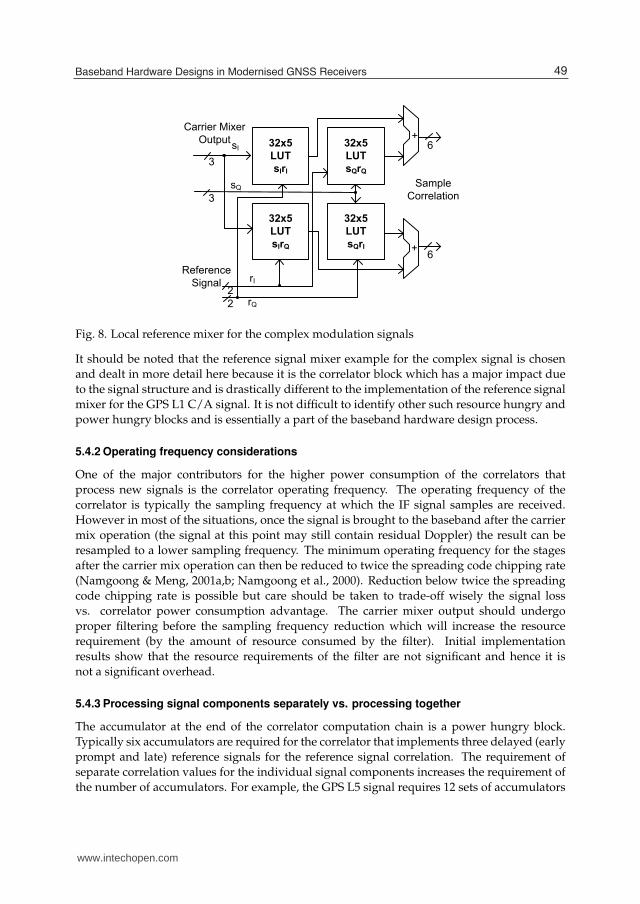
32x5
LUT
sIrI
Carrier Mixer
Output
Sample
Correlation
3
3
32x5
LUT
sQrQ
32x5
LUT
sIrQ
32x5
LUT
sQrI
sI
sQ
Reference
Signal
2
2rI
rQ
6
6+
+
Fig. 8. Local reference mixer for the complex modulation signals
It should be noted that the reference signal mixer example for the complex signal is chosen
and dealt in more detail here because it is the correlator block which has a major impact due
to the signal structure and is drastically different to the implementation of the reference signal
mixer for the GPS L1 C/A signal. It is not difficult to identify other such resource hungry and
power hungry blocks and is essentially a part of the baseband hardware design process.
5.4.2 Operating frequency considerations
One of the major contributors for the higher power consumption of the correlators that
process new signals is the correlator operating frequency. The operating frequency of the
correlator is typically the sampling frequency at which the IF signal samples are received.
However in most of the situations, once the signal is brought to the baseband after the carrier
mix operation (the signal at this point may still contain residual Doppler) the result can be
resampled to a lower sampling frequency. The minimum operating frequency for the stages
after the carrier mix operation can then be reduced to twice the spreading code chipping rate
(Namgoong & Meng, 2001a,b; Namgoong et al., 2000). Reduction below twice the spreading
code chipping rate is possible but care should be taken to trade-off wisely the signal loss
vs. correlator power consumption advantage. The carrier mixer output should undergo
proper filtering before the sampling frequency reduction which will increase the resource
requirement (by the amount of resource consumed by the filter). Initial implementation
results show that the resource requirements of the filter are not significant and hence it is
not a significant overhead.
5.4.3 Processing signal components separately vs. processing together
The accumulator at the end of the correlator computation chain is a power hungry block.
Typically six accumulators are required for the correlator that implements three delayed (early
prompt and late) reference signals for the reference signal correlation. The requirement of
separate correlation values for the individual signal components increases the requirement of
the number of accumulators. For example, the GPS L5 signal requires 12 sets of accumulators
49Baseband Hardware Designs in Modernised GNSS Receivers
www.intechopen.com

18 Will-be-set-by-IN-TECH
Signal /
Component
Correlator
Operating
Frequency
(MHz)
Resource Utilisation Power
estimate
(mW)
Registers Combina-
tional
Memory
(bits)
Galileo E5 100 667 519 - 31.98
Table 3. Resource utilisation and power consumption estimates for the Galileo E5 AltBOCcorrelator; the reference signal generation is implemented with the help of AltBOC LUT(OSSISICD, 2010)
for each channel and the Galileo E5 requires 24 accumulators per channel. Combining
the signal components before the correlation operation is possible but with significant
performance degradation. The performance degradation arises mainly due to the data-bit
ambiguity. Methods that try to avoid the data-bit ambiguity compromise on the performance
parameters of the signal in question. Therefore, again a careful consideration is required to
trade-off the performance vs. resource (or power) consumption advantage.
Table 3 shows the power consumption for the Galileo E5 AltBOC correlator if all the four
signal components are processed simultaneously. In this case there are only six accumulators
required as in the single signal component case. The reference signal in this case is generated
according to the AltBOC LUT provided in the Galileo ICD (OSSISICD, 2010). However,
the presence of data-bits (assuming that the secondary code phase resolution has already
happened) hampers the correlator output and hence the performance. Observe that the power
reduction compared to the correlator processing the signal components separately is about
19% which is a significant reduction. In other words it is possible to reduce the correlator
power consumption without losing the performance if there is a data aiding mechanism.
5.4.4 Optimising the correlator blocks across signals
Correlator design optimisation is a separate topic of itself as there are several ways to tackle
the resource utilisation issue. Moreover the optimisation is often receiver specific. Three
examples are given below where the optimisation is possible in specific correlator blocks.
First, the need for subcarrier NCO can be eliminated (even when the multiplication required
is not a power of two) by implementing clock multipliers with simple gates. For example,
in the case of Galileo E5, the x1.5 clock can be generated by simple gates that implement 32
multiplier.
Second, the carrier and code NCO for different signals from the same satellite can be
combined. This is done by programming and generating the required carrier for one of the
signals and deriving the difference in the relative Doppler for the second signal.
Third, the operating frequency for the signals can be adjusted such that the operating
frequencies can be derived from a single clock with simple dividers. The advantages of such
a clock domain construction are simplification of generation of control and timing signals as
well as ease of data transfers across different correlation stages of different signals.
50 Global Navigation Satellite Systems – Signal, Theory and Applications
www.intechopen.com

Baseband Hardware Designs in Modernised GNSS Receivers 19
6. Summary
This chapter analysed the core correlator complexities of modernised GNSS receiver baseband
hardware. A core correlator architecture description has been given and the number of bits
for the accumulator has been derived. Power consumption estimates were provided for the
new signals at the core correlator level and at the channel level.
It was shown that a GPS and Galileo civil signal receiver baseband would consume
approximately 38 times the power of a GPS L1 C/A baseband. The dominant contributor
to this increased complexity and power consumption is the Galileo E5 AltBOC signal. In
addition, implementation of the core baseband signal processing blocks in FPGA hardware
reveals up to eight times the resource requirement compared to the GPS L1 C/A only
correlator.
It is possible to optimise the hardware targeting the power consumption with the help of
resampling and external aiding. However, the performance trade-off should be carefully
looked into. Because the enormous resource and power consumption for the Galileo E5
AltBOC correlator is due to the signal structure itself, it is of interest to explore efficient
alternatives to the AltBOC signal and one such attempt is made in Shivaramaiah (2011).
Even if a dedicated Application Specific Integrated Circuit (ASIC) replaces the FPGA
baseband hardware, as a rule of thumb, and the authors’ own experience with multiple
generations of GPS L1 C/A correlator ASIC design, there will be a best case reduction of the
FPGA power consumption by a factor of 5. In other words, a baseband ASIC will consume
about 100 mW for the L1-L5 and about 200-mW for the all civil GPS+Galileo baseband.
This power consumption is very high given that it is only for the baseband hardware and
not for the entire receiver. Finally, if other global and regional satellite navigation systems
(such as GLONASS, Compass, QZSS, IRNSS) are included, then, the “200 times” estimate
of Dempster (2007) would not be far away. Hence it can be concluded that development
of a baseband hardware for the commercial general purpose multi-GNSS receiver is still a
challenging task. A direction towards a promising solution would be to explore the correlator
level reconfigurability across the GNSS signals.
7. References
Braasch, M. & van Dierendonck, A. (1999). GPS receiver architectures and measurements,
Proceedings of the IEEE.
Dempster, A. G. (2006). Correlators for L2C: Some Considerations, Inside GNSS pp. 32–37.
Dempster, A. G. (2007). Satellite navigation: New signals, new challenges, Circuits and Systems,
2007. ISCAS 2007. IEEE International Symposium on, pp. 1725 –1728.
Hegarty, C. (2009). Analytical Model for GNSS Receiver Implementation Losses, U.S. Institute
of Navigation International Technical Meeting, ION GNSS.
Kaplan, E. D. & Hegarty, C. J. (eds) (2006). Understanding GPS: Principles and Applications,
Artech House.
Namgoong, W. & Meng, T. (2001a). Minimizing power consumption in direct sequence spread
spectrum correlators by resampling IF samples-Part I: performance analysis, Circuits
and Systems II: Analog and Digital Signal Processing, IEEE Transactions on 48(5): 450–459.
51Baseband Hardware Designs in Modernised GNSS Receivers
www.intechopen.com

20 Will-be-set-by-IN-TECH
Namgoong, W. & Meng, T. (2001b). Minimizing power consumption in direct sequence
spread spectrum correlators by resampling IF samples-Part II: implementation
issues, Circuits and Systems II: Analog and Digital Signal Processing, IEEE Transactions
on 48(5): 460–470.
Namgoong, W., Reader, S. & Meng, T. (2000). An all-digital low-power IF GPS synchronizer,
Solid-State Circuits, IEEE Journal of 35(6): 856–864.
OSSISICD (2010). European gnss (galileo) open service signal in space interface control
document.
Parkinson, B. & Spilker, J. (eds) (1995). Global Positioning System: Theory and Applications,
American Institute of Aeronautics and Astronautics.
Shivaramaiah, N. C. (2004). A Fast Acquisition Hardware GPS Correlator, Master’s thesis, Center
for Electronics Design and Technology, Indian Institute of Science, Bangalore, India.
Shivaramaiah, N. C. (2011). Enhanced Receiver Techniques for Galileo E5 AltBOC Signal Processing,
PhD thesis, School of Surveying and Spatial Information Systems, University of New
South Wales, Sydney, Australia.
Shivaramaiah, N. C. & Dempster, A. G. (2009). Design challenges of a Galileo E1 correlator on
the Namuru platform, IGNSS Symp, Gold Coast, Australia.
Shivaramaiah, N. C. & Dempster, A. G. (2010). On the baseband hardware complexity of
modernized GNSS receivers, IEEE ISCAS, pp. 3565 –3568.
Shivaramaiah, N. C., Dempster, A. G. & Rizos, C. (2009). Application of Prime-factor
and Mixed-radix FFT Algorithms in Multi-band GNSS Receivers, Journal of GPS
8: 174–186.
Zarlink (1999). GPS Receiver Hardware Design Application Note AN4855, 2.0 edn, Zarlink
Semiconductor.
Zarlink (2001). GPS 12 channel correlator, issue 3.2 edn, Zarlink Semiconductor.
52 Global Navigation Satellite Systems – Signal, Theory and Applications
www.intechopen.com

Global Navigation Satellite Systems: Signal, Theory andApplicationsEdited by Prof. Shuanggen Jin
ISBN 978-953-307-843-4Hard cover, 426 pagesPublisher InTechPublished online 03, February, 2012Published in print edition February, 2012
InTech EuropeUniversity Campus STeP Ri Slavka Krautzeka 83/A 51000 Rijeka, Croatia Phone: +385 (51) 770 447 Fax: +385 (51) 686 166www.intechopen.com
InTech ChinaUnit 405, Office Block, Hotel Equatorial Shanghai No.65, Yan An Road (West), Shanghai, 200040, China
Phone: +86-21-62489820 Fax: +86-21-62489821
Global Navigation Satellite System (GNSS) plays a key role in high precision navigation, positioning, timing,and scientific questions related to precise positioning. This is a highly precise, continuous, all-weather, andreal-time technique. The book is devoted to presenting recent results and developments in GNSS theory,system, signal, receiver, method, and errors sources, such as multipath effects and atmospheric delays.Furthermore, varied GNSS applications are demonstrated and evaluated in hybrid positioning, multi-sensorintegration, height system, Network Real Time Kinematic (NRTK), wheeled robots, and status and engineeringsurveying. This book provides a good reference for GNSS designers, engineers, and scientists, as well as theuser market.
How to referenceIn order to correctly reference this scholarly work, feel free to copy and paste the following:
Nagaraj C. Shivaramaiah and Andrew G. Dempster (2012). Baseband Hardware Designs in Modernised GNSSReceivers, Global Navigation Satellite Systems: Signal, Theory and Applications, Prof. Shuanggen Jin (Ed.),ISBN: 978-953-307-843-4, InTech, Available from: http://www.intechopen.com/books/global-navigation-satellite-systems-signal-theory-and-applications/baseband-hardware-designs-in-modernised-gnss-receivers

© 2012 The Author(s). Licensee IntechOpen. This is an open access articledistributed under the terms of the Creative Commons Attribution 3.0License, which permits unrestricted use, distribution, and reproduction inany medium, provided the original work is properly cited.