Badri Complete Report
75
INTELLIGENT PATH FINDER__________________________________________ INTRODUCTION We have made an attempt to build an automatic machine which can sense the right / desired path, reach the destination and perform the desired operation. The basic wor ki ng of the ma chi ne is bas ed on the sensor ci rcui t which is suppo rt ed by the microcontroller. The machine consists of the sensor circuit placed at the base. The signals from the sensor board is given to signal conditioner circuitry and then to the microcontroller. The microcontroller is preprogrammed to react to different conditions. Depending upon the feedback from the sensor board the microcontroller diverts the machine to reach the destination. After reaching the destination the microcontroller gives signal to the winding motor to lift the tray consisti ng of 4 fuel balls and then put it in to the desired bucket. The machine is 1.5m in height, weighing approximately 10kg. It is power by a lead acid battery of 12 V, 4.5 Ahr. SARDAR PATEL COLLEGE OF ENGINEERING - 1 - Motor Control Sensor Unit MOTOR RELAY CARD WHITE LINE SENSOR SENSOR CONDIT- IONING CIRCUIT Power Supply 12v Lead Acid Battery. Processor unit / The Brain Modules ..
-
Upload
pradeesh-vasudevan -
Category
Documents
-
view
852 -
download
0
Transcript of Badri Complete Report

5/7/2018 Badri Complete Report - slidepdf.com
http://slidepdf.com/reader/full/badri-complete-report 1/74
INTELLIGENT PATH FINDER__________________________________________
INTRODUCTION
We have made an attempt to build an automatic machine which can sense the
right / desired path, reach the destination and perform the desired operation. The basic
working of the machine is based on the sensor circuit which is supported by the
microcontroller.
The machine consists of the sensor circuit placed at the base. The signals from the
sensor board is given to signal conditioner circuitry and then to the microcontroller. The
microcontroller is preprogrammed to react to different conditions. Depending upon the
feedback from the sensor board the microcontroller diverts the machine to reach the
destination. After reaching the destination the microcontroller gives signal to the winding
motor to lift the tray consisting of 4 fuel balls and then put it in to the desired bucket.
The machine is 1.5m in height, weighing approximately 10kg. It is power by a
lead acid battery of 12 V, 4.5 Ahr.
SARDAR PATEL COLLEGE OF ENGINEERING
- 1 -
Motor Control Sensor Unit
MOTOR RELAYCARD
WHITELINE
SENSOR
SENSOR CONDIT-
IONING
CIRCUIT
PowerSupply
12v Lead
Acid Battery.
Processor unit / The Brain
Modules ..

5/7/2018 Badri Complete Report - slidepdf.com
http://slidepdf.com/reader/full/badri-complete-report 2/74
INTELLIGENT PATH FINDER__________________________________________
OBJECTIVES
The primary design criteria for this robot were as follows:
- minimal cost
- incorporate already-owned components
- use cheap and easily-worked materials for platform
- minimize weight to make use of cheaper servos
- robustness
- solid design and construction
- able to be implemented in stages
- modular design
- room for expansion
The objectives for this semester were:
- design and construct the platform
- implement a simple, neural netwok based learning routine.
- implement minimal sensors for obstacle avoidance
- if time allows, implement a more intelligent moving algorithm
SARDAR PATEL COLLEGE OF ENGINEERING
- 2 -

5/7/2018 Badri Complete Report - slidepdf.com
http://slidepdf.com/reader/full/badri-complete-report 3/74
INTELLIGENT PATH FINDER__________________________________________
Microcontroller:
Atmega16 is a low-power CMOS 8-bit Micro controller based on the AVR
RISC architecture. By executing powerful instructions in a single clock cycle, the
Atmega16 achieves throughputs approaching 1 MIPS per MHz allowing the systemdesigner to optimize power consumption versus processing speed. The AVR core
combines a rich instruction set with 32 general-purpose working registers. All the 32
registers are directly connected to the Arithmetic Logic Unit (ALU), allowing two
independent registers to be accessed in one single instruction executed in one clock cycle.
The resulting architecture is more code efficient while achieving throughputs up to ten
times faster than conventional CISC Micro controller.
The ATmega16 provides the following features: 16K bytes of In-System
Programmable Flash Program memory with Read-While-Write capabilities, 512 bytes
EEPROM, 1K byte SRAM, 32 general purpose I/O lines, 32 general purpose working
registers, a JTAG interface for Boundary-scan, On-chip Debugging support and
programming, three flexible Timer/Counters with compare modes, Internal and External
Interrupts, a serial programmable USART, a byte oriented Two-wire Serial Interface, an
8-channel, 10-bit ADC with optional differential input stage with programmable gain
(TQFP package only), a programmable Watchdog Timer with Internal Oscillator, an SPI
serial port, and six software selectable power saving modes. The Idle mode stops the
CPU while allowing the USART, Two-wire interface, A/D Converter, SRAM,
Timer/Counters, SPI port, and interrupt system to continue functioning. The Power-down
mode saves the register contents but freezes the Oscillator, disabling all other chip
functions until the next External Interrupt or Hardware Reset. In Power-save mode, the
Asynchronous Timer continues to run, allowing the user to maintain a timer base while
the rest of the device is sleeping. The ADC Noise Reduction mode stops the CPU and all
I/O modules except Asynchronous Timer and ADC, to minimize switching noise during
ADC conversions. In Standby mode, the crystal/resonator Oscillator is running while the
rest of the device is sleeping. This allows very fast start-up combined with low-power
consumption. In Extended Standby mode, both the main Oscillator and the Asynchronous
Timer continue to run.
SARDAR PATEL COLLEGE OF ENGINEERING
- 3 -

5/7/2018 Badri Complete Report - slidepdf.com
http://slidepdf.com/reader/full/badri-complete-report 4/74
INTELLIGENT PATH FINDER__________________________________________
The device is manufactured using Atmel’s high-density nonvolatile memory
technology. The On-chip ISP Flash allows the program memory to be reprogrammed in-
system through an SPI serial interface, by a conventional nonvolatile memory
programmer, or by an On-chip Boot program running on the AVR core. The boot
program can use any interface to download the application program in the Application
Flash memory. Software in the Boot Flash section will continue to run while the
Application Flash section is updated, providing true Read-While-Write operation. By
combining an 8-bit RISC CPU with In-System Self-Programmable Flash on a monolithic
chip, the Atmel ATmega16 is a powerful microcontroller that provides a highly-flexible
and cost-effective solution to many embedded control applications.
The ATmega16 AVR is supported with a full suite of program and system
development tools including: C compilers, macro assemblers, program
debugger/simulators, in-circuit emulators, and evaluation kits.
SARDAR PATEL COLLEGE OF ENGINEERING
- 4 -

5/7/2018 Badri Complete Report - slidepdf.com
http://slidepdf.com/reader/full/badri-complete-report 5/74
INTELLIGENT PATH FINDER__________________________________________
Figure 1: Block Diagram
SARDAR PATEL COLLEGE OF ENGINEERING
- 5 -

5/7/2018 Badri Complete Report - slidepdf.com
http://slidepdf.com/reader/full/badri-complete-report 6/74
INTELLIGENT PATH FINDER__________________________________________
Features:
• High-performance, Low-power AVR® 8-bit Microcontroller
• Advanced RISC Architecture
– 131 Powerful Instructions – Most Single-clock Cycle Execution
– 32 x 8 General Purpose Working Registers
– Fully Static Operation
– Up to 16 MIPS Throughput at 16 MHz
– On-chip 2-cycle Multiplier
• Nonvolatile Program and Data Memories
– 16K Bytes of In-System Self-Programmable Flash
Endurance: 10,000 Write/Erase Cycles
– Optional Boot Code Section with Independent Lock Bits
In-System Programming by On-chip Boot Program
True Read-While-Write Operation
– 512 Bytes EEPROM
Endurance: 100,000 Write/Erase Cycles
– 1K Byte Internal SRAM
– Programming Lock for Software Security
• JTAG (IEEE std. 1149.1 Compliant) Interface
– Boundary-scan Capabilities According to the JTAG Standard
– Extensive On-chip Debug Support
– Programming of Flash, EEPROM, Fuses, and Lock Bits through the JTAG Interface
• Peripheral Features
– Two 8-bit Timer/Counters with Separate Prescalers and Compare Modes
– One 16-bit Timer/Counter with Separate Prescaler, Compare Mode, and Capture
Mode
– Real Time Counter with Separate Oscillator
– Four PWM Channels
– 8-channel, 10-bit ADC
8 Single-ended Channels
7 Differential Channels in TQFP Package Only
SARDAR PATEL COLLEGE OF ENGINEERING
- 6 -

5/7/2018 Badri Complete Report - slidepdf.com
http://slidepdf.com/reader/full/badri-complete-report 7/74
INTELLIGENT PATH FINDER__________________________________________
2 Differential Channels with Programmable Gain at 1x, 10x, or 200x
– Byte-oriented Two-wire Serial Interface
– Programmable Serial USART
– Master/Slave SPI Serial Interface
– Programmable Watchdog Timer with Separate On-chip Oscillator
– On-chip Analog Comparator
• Special Microcontroller Features
– Power-on Reset and Programmable Brown-out Detection
– Internal Calibrated RC Oscillator
– External and Internal Interrupt Sources
– Six Sleep Modes: Idle, ADC Noise Reduction, Power-save, Power-down, Standby
and Extended Standby
• I/O and Packages
– 32 Programmable I/O Lines
– 40-pin PDIP, 44-lead TQFP, and 44-pad MLF
• Operating Voltages
– 2.7 - 5.5V for ATmega16L
– 4.5 - 5.5V for ATmega16
• Speed Grades – 0 - 8 MHz for ATmega16L
– 0 - 16 MHz for ATmega16
• Power Consumption @ 1 MHz, 3V, and 25 C for ATmega16L
– Active: 1.1 mA
– Idle Mode: 0.35 mA
Power-down Mode: < 1 µA
SARDAR PATEL COLLEGE OF ENGINEERING
- 7 -

5/7/2018 Badri Complete Report - slidepdf.com
http://slidepdf.com/reader/full/badri-complete-report 8/74
INTELLIGENT PATH FINDER__________________________________________
Figure 2. Pinouts ATmega16
SARDAR PATEL COLLEGE OF ENGINEERING
- 8 -

5/7/2018 Badri Complete Report - slidepdf.com
http://slidepdf.com/reader/full/badri-complete-report 9/74
INTELLIGENT PATH FINDER__________________________________________
Pin Description:
SARDAR PATEL COLLEGE OF ENGINEERING
- 9 -
Vcc Digital supply voltage.
GND Ground
Port A
(PA7..PA0
)
Port A serves as the analog inputs to the A/D Converter.
Port A also serves as an 8-bit bi-directional I/O port, if the A/D Converter
is not used. Port pins can provide internal pull-up resistors (selected for each bit). The Port A output buffers have symmetrical drive characteristics
with both high sink and source capability. When pins PA0 to PA7 are used
as inputs and are externally pulled low, they will source current if theinternal pull-up resistors are activated. The Port A pins are tri-stated when
a reset condition becomes active, even if the clock is not running.
Port B
(PB7..PB0)
Port B is an 8-bit bi-directional I/O port with internal pull-up resistors
(selected for each bit). The Port B output buffers have symmetrical drivecharacteristics with both high sink and source capability. As inputs, Port B
pins that are externally pulled low will source current if the pull-upresistors are activated. The Port B pins are tri-stated when a reset condition
becomes active, even if the clock is not running. Port B also serves the
functions of various special features of the ATmega16.
Port C
(PC7..PC0
)
Port C is an 8-bit bi-directional I/O port with internal pull-up resistors
(selected for each bit). The Port C output buffers have symmetrical drivecharacteristics with both high sink and source capability. As inputs, Port C
pins that are externally pulled low will source current if the pull-up
resistors are activated. The Port C pins are tri-stated when a reset condition becomes active, even if the clock is not running. If the JTAG interface isenabled, the pull-up resistors on pins PC5(TDI), PC3(TMS) and
PC2(TCK) will be activated even if a reset occurs.
Port C also serves the functions of the JTAG interface and other specialfeatures of the ATmega16.
Port D
(PD7..PD0
)
Port D is an 8-bit bi-directional I/O port with internal pull-up resistors(selected for each bit). The Port D output buffers have symmetrical drive
characteristics with both high sink and source capability. As inputs, Port D
pins that are externally pulled low will source current if the pull-up
resistors are activated. The Port D pins are tri-stated when a reset condition becomes active, even if the clock is not running. Port D also serves the
functions of various special features of the ATmega16.

5/7/2018 Badri Complete Report - slidepdf.com
http://slidepdf.com/reader/full/badri-complete-report 10/74
INTELLIGENT PATH FINDER__________________________________________
SARDAR PATEL COLLEGE OF ENGINEERING
- 10 -
RESET Reset Input. A low level on this pin for longer than the minimum pulse
length will generate a reset, even if the clock is not running. The minimum
pulse length is given in Table 15 on page 36. Shorter pulses are notguaranteed to generate a reset.
XTAL1 Input to the inverting Oscillator amplifier and input to the internal clock operating circuit.
XTAL2 Output from the inverting Oscillator amplifier.
AVCC AVCC is the supply voltage pin for Port A and the A/D Converter. It should
be externally connected to VCC, even if the ADC is not used. If the ADC isused, it should be connected to VCC through a low-pass filter.
AREF AREF is the analog reference pin for the A/D Converter

5/7/2018 Badri Complete Report - slidepdf.com
http://slidepdf.com/reader/full/badri-complete-report 11/74
INTELLIGENT PATH FINDER__________________________________________
16-bit Timer/Counter:
The 16-bit Timer/Counter unit allows accurate program execution timing (event
management), wave generation, and signal timing measurement. The main features are:
• True 16-bit Design (i.e., Allows 16-bit PWM)
• Two Independent Output Compare Units
• Double Buffered Output Compare Registers
• One Input Capture Unit
• Input Capture Noise Canceler
• Clear Timer on Compare Match (Auto Reload)
• Glitch-free, Phase Correct Pulse Width Modulator (PWM)
• Variable PWM Period
• Frequency Generator
• External Event Counter
• Four Independent Interrupt Sources (TOV1, OCF1A, OCF1B, and ICF1)
Overview
Most register and bit references in this section are written in general form. A
lower case“n” replaces the Timer/Counter number, and a lower case “x” replaces the
output compare unit channel. However, when using the register or bit defines in a
program, the precise form must be used (i.e., TCNT1 for accessing Timer/Counter
counter value and so on).
A simplified block diagram of the 16-bit Timer/Counter is shown below in Figure. CPU
accessible I/O Registers, including I/O bits and I/O pins, are shown in bold. The device
specific I/O Register and bit locations are listed in the “16-bit Timer/Counter Register
Description” are given below.
SARDAR PATEL COLLEGE OF ENGINEERING
- 11 -

5/7/2018 Badri Complete Report - slidepdf.com
http://slidepdf.com/reader/full/badri-complete-report 12/74
INTELLIGENT PATH FINDER__________________________________________
16-bit Timer/Counter Block Diagram.
SARDAR PATEL COLLEGE OF ENGINEERING
- 12 -
5/7/2018 Badri Complete Report - slidepdf.com
http://slidepdf.com/reader/full/badri-complete-report 13/74
INTELLIGENT PATH FINDER__________________________________________
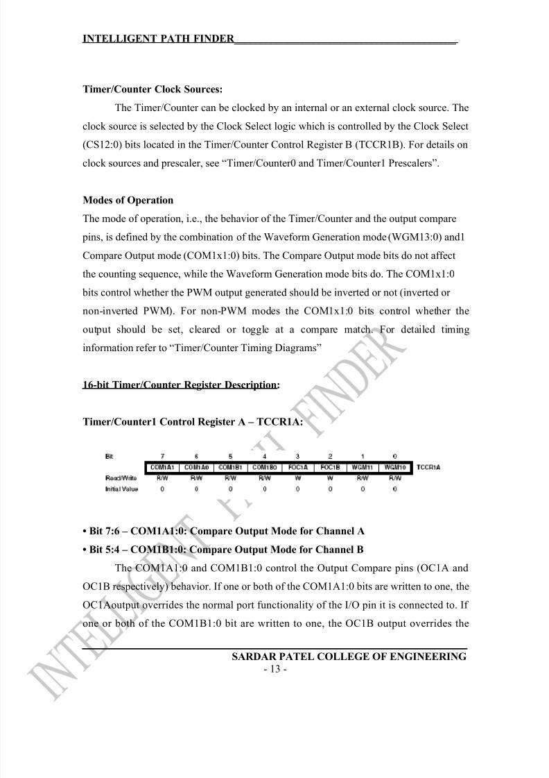
Timer/Counter Clock Sources:
The Timer/Counter can be clocked by an internal or an external clock source. The
clock source is selected by the Clock Select logic which is controlled by the Clock Select
(CS12:0) bits located in the Timer/Counter Control Register B (TCCR1B). For details on
clock sources and prescaler, see “Timer/Counter0 and Timer/Counter1 Prescalers”.
Modes of Operation
The mode of operation, i.e., the behavior of the Timer/Counter and the output compare
pins, is defined by the combination of the Waveform Generation mode (WGM13:0) and1
Compare Output mode (COM1x1:0) bits. The Compare Output mode bits do not affect
the counting sequence, while the Waveform Generation mode bits do. The COM1x1:0
bits control whether the PWM output generated should be inverted or not (inverted or
non-inverted PWM). For non-PWM modes the COM1x1:0 bits control whether the
output should be set, cleared or toggle at a compare match. For detailed timing
information refer to “Timer/Counter Timing Diagrams”
16-bit Timer/Counter Register Description:
Timer/Counter1 Control Register A – TCCR1A:
• Bit 7:6 – COM1A1:0: Compare Output Mode for Channel A
• Bit 5:4 – COM1B1:0: Compare Output Mode for Channel B
The COM1A1:0 and COM1B1:0 control the Output Compare pins (OC1A and
OC1B respectively) behavior. If one or both of the COM1A1:0 bits are written to one, the
OC1Aoutput overrides the normal port functionality of the I/O pin it is connected to. If
one or both of the COM1B1:0 bit are written to one, the OC1B output overrides the
SARDAR PATEL COLLEGE OF ENGINEERING
- 13 -

5/7/2018 Badri Complete Report - slidepdf.com
http://slidepdf.com/reader/full/badri-complete-report 14/74
INTELLIGENT PATH FINDER__________________________________________
normal port functionality of the I/O pin it is connected to. However, note that the Data
Direction Register(DDR) bit corresponding to the OC1A or OC1B pin must be set in
order to enable the output driver. When the OC1A or OC1B is connected to the pin, the
function of the COM1x1:0 bits is dependent of the WGM13:0 bits setting. Table 44
shows the COM1x1:0 bit functionality when the WGM13:0 bits are set to a normal or a
CTC mode (non-PWM).
Compare Output Mode, non-PWM
Table shows the COM1x1:0 bit functionality when the WGM13:0 bits are set to the fast
PWM mode.
Compare Output Mode, Fast PWM
Note : A special case occurs when OCR1A/OCR1B equals TOP and COM1A1/COM1B1
is set. In this case the compare match is ignored, but the set or clear is done at TOP.
Table shows the COM1x1:0 bit functionality when the WGM13:0 bits are set to the phase
correct or the phase and frequency correct, PWM mode. Compare Output Mode, Phase
Correct and Phase and Frequency Correct PWM
SARDAR PATEL COLLEGE OF ENGINEERING
- 14 -

5/7/2018 Badri Complete Report - slidepdf.com
http://slidepdf.com/reader/full/badri-complete-report 15/74
INTELLIGENT PATH FINDER__________________________________________
Note: A special case occurs when OCR1A/OCR1B equals TOP and COM1A1/COM1B1
is set.
• Bit 3 – FOC1A: Force Output Compare for Channel A
• Bit 2 – FOC1B: Force Output Compare for Channel B
The FOC1A/FOC1B bits are only active when the WGM13:0 bits specifies a non-
PWM mode. However, for ensuring compatibility with future devices, these bits must be
set to zero when TCCR1A is written when operating in a PWM mode. When writing a
logical one to the FOC1A/FOC1B bit, an immediate compare match is forced on the
Waveform Generation unit. The OC1A/OC1B output is changed according to its
COM1x1:0 bits setting. Note that the FOC1A/FOC1B bits are implemented as strobes.
Therefore it is the value present in the COM1x1:0 bits that determine the effect of the
forced compare.
A FOC1A/FOC1B strobe will not generate any interrupt nor will it clear the timer
in Clear Timer on Compare match (CTC) mode using OCR1A as TOP. The
FOC1A/FOC1B bits are lways read as zero.
SARDAR PATEL COLLEGE OF ENGINEERING
- 15 -

5/7/2018 Badri Complete Report - slidepdf.com
http://slidepdf.com/reader/full/badri-complete-report 16/74
INTELLIGENT PATH FINDER__________________________________________
• Bit 1:0 – WGM11:0: Waveform Generation Mode
Combined with the WGM13:2 bits found in the TCCR1B Register, these bits
control the counting sequence of the counter, the source for maximum (TOP) counter
value, and what type of waveform generation to be used, see table Modes of operation
supported by the Timer/Counter unit are: Normal mode (counter), Clear Timer on
Compare match (CTC) mode, and three types of pulse Width Modulation (PWM)
modes.
Waveform Generation Mode Bit Description(1)
Note: 1. The CTC1 and PWM11:0 bit definition names are obsolete. Use the WGM12:0
definitions. However, the functionality and location of these bits are compatible with
previous versions of the timer.
SARDAR PATEL COLLEGE OF ENGINEERING
- 16 -

5/7/2018 Badri Complete Report - slidepdf.com
http://slidepdf.com/reader/full/badri-complete-report 17/74
INTELLIGENT PATH FINDER__________________________________________
Timer/Counter1 Control Register B – TCCR1B
• Bit 7 – ICNC1: Input Capture Noise Canceler
Setting this bit (to one) activates the Input Capture Noise Canceler. When the
Noise canceler is activated, the input from the Input Capture Pin (ICP1) is filtered. The
filter function requires four successive equal valued samples of the ICP1 pin for changing
its output. The Input Capture is therefore delayed by four Oscillator cycles when the
Noise Canceler is enabled.
• Bit 6 – ICES1: Input Capture Edge Select
This bit selects which edge on the Input Capture Pin (ICP1) that is used to trigger
a capture event. When the ICES1 bit is written to zero, a falling (negative) edge is used
as trigger, and when the ICES1 bit is written to one, a rising (positive) edge will trigger
the capture. When a capture is triggered according to the ICES1 setting, the counter value
is copied into the Input Capture Register (ICR1). The event will also set the Input
Capture lag (ICF1), and this can be used to cause an Input Capture Interrupt, if this
interrupt is enabled. When the ICR1 is used as TOP value (see description of the
WGM13:0 bits located in the TCCR1A and the TCCR1B Register), the ICP1 is
disconnected and consequently the Input Capture function is disabled.
• Bit 5 – Reserved Bit
This bit is reserved for future use. For ensuring compatibility with future devices, this bit
must be written to zero when TCCR1B is written.
• Bit 4:3 – WGM13:2: Waveform Generation Mode
SARDAR PATEL COLLEGE OF ENGINEERING
- 17 -

5/7/2018 Badri Complete Report - slidepdf.com
http://slidepdf.com/reader/full/badri-complete-report 18/74
INTELLIGENT PATH FINDER__________________________________________
• Bit 2:0 – CS12:0: Clock Select
The three Clock Select bits select the clock source to be used by the Timer/Counter
Clock Select Bit Description
Clock Select Bit Description
If external pin modes are used for the Timer/Counter1, transitions on the T1 pin will
clock the counter even if the pin is configured as an output. This feature allows software
control of the counting.
Timer/Counter1 – TCNT1H and TCNT1L
The two Timer/Counter I/O locations (TCNT1H and TCNT1L, combined
TCNT1) give direct access, both for read and for write operations, to the Timer/Counter
unit 16-bit counter. To ensure that both the high and Low bytes are read and written
simultaneously when the CPU accesses these registers, the access is performed using an
8-bit temporary High Byte Register (TEMP). This temporary register is shared by all the
other 16-bit registers. Modifying the counter (TCNT1) while the counter is running
introduces a risk missing compare match between TCNT1 and one of the OCR1x
Registers. Writing to the TCNT1 Register blocks (removes) the compare match on the
following timer clock for all compare units.
SARDAR PATEL COLLEGE OF ENGINEERING
- 18 -

5/7/2018 Badri Complete Report - slidepdf.com
http://slidepdf.com/reader/full/badri-complete-report 19/74
INTELLIGENT PATH FINDER__________________________________________
Output Compare Register 1 A – OCR1AH and OCR1AL
Output Compare Register 1 B – OCR1BH and OCR1BL
The Output Compare Registers contain a 16-bit value that is continuously
compared with the counter value (TCNT1). A match can be used to generate an outputcompare interrupt, or to generate a waveform output on the OC1x pin. The Output
Compare Registers are 16-bit in size. To ensure that both the high and Low bytes are
written simultaneously when the CPU writes to these registers, the access is performed
using an 8-bit temporary High Byte Register (TEMP). This temporary register is shared
by all the other 16-bit registers.
Input Capture Register 1 – ICR1H and ICR1L
The Input Capture is updated with the counter (TCNT1) value each time an event
occurs on the ICP1 pin (or optionally on the analog comparator output for
Timer/Counter1). The Input Capture can be used for defining the counter TOP value. The
Input Capture Register is 16-bit in size. To ensure that both the high and Low bytes are
read simultaneously when the CPU accesses these registers, the access is performed using
an 8-bit temporary High Byte Register (TEMP). This temporary register is shared by all
the other 16-bit registers.
SARDAR PATEL COLLEGE OF ENGINEERING
- 19 -

5/7/2018 Badri Complete Report - slidepdf.com
http://slidepdf.com/reader/full/badri-complete-report 20/74
INTELLIGENT PATH FINDER__________________________________________
Timer/Counter Interrupt Mask Register – TIMSK
Note: 1. This register contains interrupt control bits for several Timer/Counters, but only
Timer1 bits are described in this section. The remaining bits are described in their
respective timer sections.
• Bit 5 – TICIE1: Timer/Counter1, Input Capture Interrupt Enable
When this bit is written to one, and the I-flag in the Status Register is set (interrupts
globally enabled), the Timer/Counter1 Input Capture Interrupt is enabled. The
corresponding Interrupt Vector is executed when the ICF1 Flag, located in TIFR, is set.
• Bit 4 – OCIE1A: Timer/Counter1, Output Compare A Match Interrupt Enable
When this bit is written to one, and the I-flag in the Status Register is set (interrupts
globally enabled), the Timer/Counter1 Output Compare A match interrupt is enabled.
The corresponding Interrupt Vector is executed when the OCF1A Flag, located in TIFR,
is set.
• Bit 3 – OCIE1B: Timer/Counter1, Output Compare B Match Interrupt Enable
When this bit is written to one, and the I-flag in the Status Register is set (interrupts
globally enabled), the Timer/Counter1 Output Compare B match interrupt is enabled. The
corresponding Interrupt Vector is executed when the OCF1B Flag, located in TIFR, is
set.
• Bit 2 – TOIE1: Timer/Counter1, Overflow Interrupt Enable
When this bit is written to one, and the I-flag in the Status Register is set (interrupts
globally enabled), the Timer/Counter1 Overflow Interrupt is enabled. The corresponding
Interrupt Vector is executed when the TOV1 Flag, located in TIFR, is set.
SARDAR PATEL COLLEGE OF ENGINEERING
- 20 -

5/7/2018 Badri Complete Report - slidepdf.com
http://slidepdf.com/reader/full/badri-complete-report 21/74
INTELLIGENT PATH FINDER__________________________________________
Timer/Counter Interrupt Flag Register – TIFR
Note: This register contains flag bits for several Timer/Counters, but only Timer1 bits are
described in this section. The remaining bits are described in their respective timer
sections.
• Bit 5 – ICF1: Timer/Counter1, Input Capture Flag
This flag is set when a capture event occurs on the ICP1 pin. When the Input Capture
Register (ICR1) is set by the WGM13:0 to be used as the TOP value, the ICF1 Flag is set
when the counter reaches the TOP value. ICF1 is automatically cleared when the InputCapture Interrupt Vector is executed. Alternatively, ICF1 can be cleared by writing a
logic one to its bit location.
• Bit 4 – OCF1A: Timer/Counter1, Output Compare A Match Flag
This flag is set in the timer clock cycle after the counter (TCNT1) value matches the
output Compare Register A (OCR1A). Note that a Forced Output Compare (FOC1A)
strobe will not set the OCF1A Flag. OCF1A is automatically cleared when the Output
compare Match A Interrupt Vector is executed. Alternatively, OCF1A can be cleared by
writing a logic one to its bit location.
• Bit 3 – OCF1B: Timer/Counter1, Output Compare B Match Flag
This flag is set in the timer clock cycle after the counter (TCNT1) value matches the
Output Compare Register B (OCR1B). Note that a forced output compare (FOC1B)
probe will not set the OCF1B Flag. OCF1B is automatically cleared when the Output
compare Match B Interrupt Vector is executed. Alternatively, OCF1B can be cleared by
writing a logic one to its bit location.
SARDAR PATEL COLLEGE OF ENGINEERING
- 21 -

5/7/2018 Badri Complete Report - slidepdf.com
http://slidepdf.com/reader/full/badri-complete-report 22/74
INTELLIGENT PATH FINDER__________________________________________
• Bit 2 – TOV1: Timer/Counter1, Overflow Flag
The setting of this flag is dependent of the WGM13:0 bits setting. In normal and CTC
modes, the TOV1 Flag is set when the timer overflows. Refer to Table 47 on page 111
for the TOV1 Flag behavior when using another WGM13:0 bit setting. TOV1 is
automatically cleared when the Timer/Counter1 Overflow interrupt vector is executed.
Alternatively, TOV1 can be cleared by writing a logic one to its bit location.
SARDAR PATEL COLLEGE OF ENGINEERING
- 22 -

5/7/2018 Badri Complete Report - slidepdf.com
http://slidepdf.com/reader/full/badri-complete-report 23/74
INTELLIGENT PATH FINDER__________________________________________
SENSORS :
Sensors are used as the eyes of the robot. They keep informing the position of the
robot on the track. There are two types of the sensors used, infrared sensors and colour
sensors. Sensing is based on the reflection of light from the surface.
INFRARED SENSOR :
Infrared sensors are operated in the infrared light rays. The working principle of
IR sensor is that infrared rays will get reflected from the silver surface and will not get
reflected from the black surface, because black surface will absorb the maximum amount
light rays falling on it. IR sensors include infrared transmitter (IR Led) and infrared
receiver. IR led and IR receiver is placed side by side. These sensors are placed at the
bottom surface of the robot facing toward the ground. IR led will emit the infrared light
rays. These rays will fall on the surface and reflected by the surface. These reflected rays
will fall on the IR receiver. When sufficient amount of light falls on the IR receiver, it
will start conducting. When IR transmitter receiver is on the black surface most of the
light will be absorbed by the surface and receiver is open and when they are on silver
strip the receiver gets enough light and starts conducting.
IR led is connected to VCC through resistance of small value. IR receiver is
connected to VCC through 10K resistance. The output is taken across the receiver and the
ground. This output voltage is not enough for the microcontroller to take the decisions.
So the signal conditioning is required. The signal conditioner includes a comparator
circuit and a reference voltage. The reference voltage is generated with potentiometer.
The reference voltage level is arranged in such a way that it is in between the two voltage
levels that were get from the black and silver surface. When sensor is on the black
surface receiver is open the voltage get pulled up to VCC and when it is on silver surface
receiver will shorted and the voltage is pulled down to GND.
The circuit used for the IR detector is shown below. Quad OP-AMP LM324 is
used as a comparator. Supply voltage is 5V. Inverting terminal of LM324 is connected to
the reference voltage through the variable potentiometer of 10MΩ. non-inverting
terminal is connected to the output from the IR receiver.
SARDAR PATEL COLLEGE OF ENGINEERING
- 23 -

5/7/2018 Badri Complete Report - slidepdf.com
http://slidepdf.com/reader/full/badri-complete-report 24/74
INTELLIGENT PATH FINDER__________________________________________
1 0 k
I R L E D
L E D
I R R E C E I V E R
1 2 0
1 0 M
V A R R E S I S T O R
T O M I C R O C O N T R O L L E R
5 V V C C
1 2 0
O P A M P+
-
O U T
Circuit diagram of IR sensor
Drawbacks of IR sensor:
The response of IR sensors is good only on silver track on black surface. On the
other type of track its response is not good enough.
COLOUR SENSOR:
The color of the objects which we see are largely due to the way those objectsinteract with light and ultimately reflect or transmit it to our eyes. The color of an object
is not actually within the object itself; rather, the color is in the light which shines upon it
that ultimately becomes reflected or transmitted to our eyes. We know that the visible
light spectrum consists of a range of frequencies, each of which corresponds to a specific
color. When visible light strikes an object and a specific frequency becomes absorbed,
that frequency of light will never make it to our eyes. Any visible light which strikes the
object and becomes reflected or transmitted to our eyes will contribute to the color
appearance of that object. So the color is not in the object itself, but in the light which
strikes the object. The only role that the object plays is that it might contain atoms
capable of absorbing one or more frequencies of the visible light which shine upon it. So
if an object absorbs all of the frequencies of visible light except for the frequency
associated with green light, then the object will appear green in the presence of
SARDAR PATEL COLLEGE OF ENGINEERING
- 24 -
5/7/2018 Badri Complete Report - slidepdf.com
http://slidepdf.com/reader/full/badri-complete-report 25/74
INTELLIGENT PATH FINDER__________________________________________
ROYGBIV. And if an object absorbs all of the frequencies of visible light except for the
frequency associated with blue light, then the object will appear blue in the presence of
ROYGBIV.
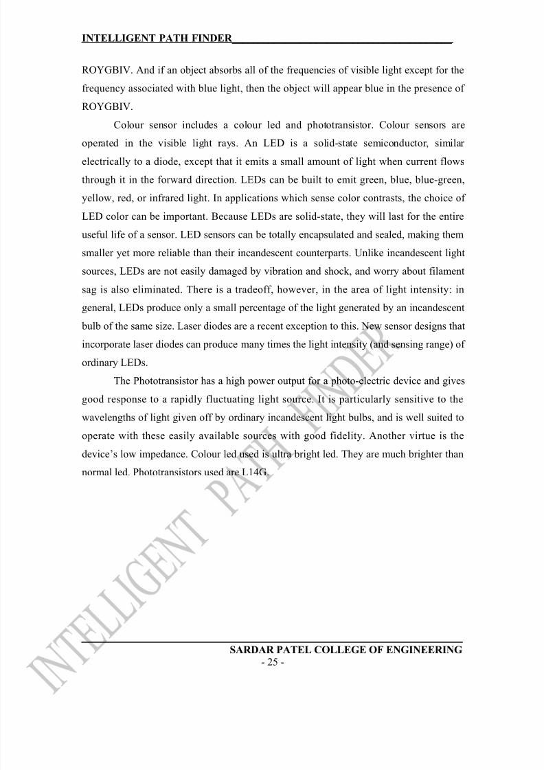
Colour sensor includes a colour led and phototransistor. Colour sensors are
operated in the visible light rays. An LED is a solid-state semiconductor, similar
electrically to a diode, except that it emits a small amount of light when current flows
through it in the forward direction. LEDs can be built to emit green, blue, blue-green,
yellow, red, or infrared light. In applications which sense color contrasts, the choice of
LED color can be important. Because LEDs are solid-state, they will last for the entire
useful life of a sensor. LED sensors can be totally encapsulated and sealed, making them
smaller yet more reliable than their incandescent counterparts. Unlike incandescent light
sources, LEDs are not easily damaged by vibration and shock, and worry about filament
sag is also eliminated. There is a tradeoff, however, in the area of light intensity: in
general, LEDs produce only a small percentage of the light generated by an incandescent
bulb of the same size. Laser diodes are a recent exception to this. New sensor designs that
incorporate laser diodes can produce many times the light intensity (and sensing range) of
ordinary LEDs.
The Phototransistor has a high power output for a photo-electric device and gives
good response to a rapidly fluctuating light source. It is particularly sensitive to thewavelengths of light given off by ordinary incandescent light bulbs, and is well suited to
operate with these easily available sources with good fidelity. Another virtue is the
device’s low impedance. Colour led used is ultra bright led. They are much brighter than
normal led. Phototransistors used are L14G.
SARDAR PATEL COLLEGE OF ENGINEERING
- 25 -

5/7/2018 Badri Complete Report - slidepdf.com
http://slidepdf.com/reader/full/badri-complete-report 26/74
INTELLIGENT PATH FINDER__________________________________________
Phototransistor L14G Symbol of photo transistor
Spectral Response of phototransistor
A phototransistor is a transistor whose collector and emitter currents are directly
related to the light incident on the base region of the transistor. Although any transistor
will respond to light, the phototransistor has some features that make it more sensitive at
certain wavelengths of light.
When the base is illuminated with the correct wavelength of light, electron-hole
pairs are formed in the base which creates a base current, with the current flow directly
related to the brightness of the light. The main region for the electron-hole pair formation
is the base-collector junction. The photo-induced base current appears as though an
external diode was connected between the base and collector of the transistor, see Figur
SARDAR PATEL COLLEGE OF ENGINEERING
- 26 -

5/7/2018 Badri Complete Report - slidepdf.com
http://slidepdf.com/reader/full/badri-complete-report 27/74
INTELLIGENT PATH FINDER__________________________________________
The phototransistor and the equivalent circuit with a reverse
biased diode
The principle of operation of colour sensor is based on the amount of reflection
of light from different colour surfaces. Colour sensors can be used to track any type of
track. Led and phototransistor is arranged side by side. To track any type of path four
sensors are more than enough. They are arranged in plus format as shown below. If the
width of track changes we have to just change the distance ‘a’. This arrangement is
placed at the bottom of the robot facing towards track. ‘F’ denotes front, ‘L’ denotes left,
‘R’ denotes right, ‘B’ denotes back sensor. The robot will try to arrange itself in such a
way that F and B will be on the track and L and R are off the track. The distance of the
arrangement from the ground is critical. According to this distance we have to change the
reference voltage.
SARDAR PATEL COLLEGE OF ENGINEERING
- 27 -

5/7/2018 Badri Complete Report - slidepdf.com
http://slidepdf.com/reader/full/badri-complete-report 28/74
INTELLIGENT PATH FINDER__________________________________________
Arrangement of led and phototransistor
F
a
L R
Tx Rx
B
Arrangement of sensors
Robot can get off the track due to some obstacle. With this arrangement of
sensors, to follow the path atleast one sensor has to be there on the track. If all the sensors
are get off the track then robot may not follow the desired path. For this extra sensors has
been added to the above arrangement. An array of sensors have been added beside the left
and right sensor to increase the range of robot.
SARDAR PATEL COLLEGE OF ENGINEERING
- 28 -

5/7/2018 Badri Complete Report - slidepdf.com
http://slidepdf.com/reader/full/badri-complete-report 29/74
INTELLIGENT PATH FINDER__________________________________________
F
B
Modified arrangement of sensors
The circuit diagram of the colour sensor is as shown below. Transmitter is
connected to the supply through resistor of 1KΩ. Phototransistor is connected in series
with 47KΩ resistor. The output voltage is taken across the collector of phototransistor
and GND. This voltage is connected to the signal conditioning circuitry. Single
conditioning circuitry includes reference voltage, buffers and subtractor. Reference
voltage and the output from phototransistor are buffered through unity gain amplifier.These buffered signals are subtracted and the output is buffered. Reference voltage level
is adjusted in between the two voltage levels that are obtained from two different colours.
SARDAR PATEL COLLEGE OF ENGINEERING
- 29 -

5/7/2018 Badri Complete Report - slidepdf.com
http://slidepdf.com/reader/full/badri-complete-report 30/74
INTELLIGENT PATH FINDER__________________________________________
Circuit Diagram of colour sensor
SARDAR PATEL COLLEGE OF ENGINEERING
- 30 -

5/7/2018 Badri Complete Report - slidepdf.com
http://slidepdf.com/reader/full/badri-complete-report 31/74
INTELLIGENT PATH FINDER__________________________________________
Motor:
How does a motor work?
Let's consider a permanent magnet brushed motor. The piece connected to the
ground is called the stator and the piece connected to the output shaft is called the rotor.
The inputs of the motor are connected to 2 wires and by applying a voltage across them,
the motor turns.
The torque of a motor is generated by a current carrying conductor in a magnetic
field. The right hand rule states that if you point your right hand fingers along the
direction of current, I, and curl them towards the direction of the magnetic flux, B, the
direction of force is along the thumb.
The bar magnet represents the armature and the coil of wire represents the field. The
arrow shows the direction of the armature's rotation. Notice that the arrow shows the
SARDAR PATEL COLLEGE OF ENGINEERING
- 31 -

5/7/2018 Badri Complete Report - slidepdf.com
http://slidepdf.com/reader/full/badri-complete-report 32/74
INTELLIGENT PATH FINDER__________________________________________
armature starting to rotate in the clockwise direction. The north pole of the field coil is
repelling the north pole of the armature, and the south pole of the field coil is repelling
the south pole of the armature.
(a) Magnetic diagram that explains the operation of a DC motor. The rotating magnet
moves clockwise because like poles repel. (b) The rotating magnet is being attracted
because the poles are unlike. (c) The rotating magnet is now shown as the armature coil,
and its polarity is determined by the brushes and commutator segments.
SARDAR PATEL COLLEGE OF ENGINEERING
- 32 -

5/7/2018 Badri Complete Report - slidepdf.com
http://slidepdf.com/reader/full/badri-complete-report 33/74
INTELLIGENT PATH FINDER__________________________________________
As the armature begins to move, the north pole of the armature comes closer to
the south pole of the field, and the south pole of the armature is coming closer to the
north pole of the field. As the two unlike poles near each other, they begin to attract. This
attraction becomes stronger until the armature's north pole moves directly in line with the
field's south pole, and its south pole moves directly in line with the field's north pole.
When the opposite poles are at their strongest attraction, the armature will be
"locked up" and will resist further attempts to continue spinning. For the armature to
continue its rotation, the armature's polarity must be switched. Since the armature in this
diagram is a permanent magnet, you can see that it would lock up during the first rotation
and not work. If the armature is an electromagnet, its polarity can be changed by
changing the direction of current flow through it. For this reason the armature must be
changed to a coil (electromagnet) and a set of commutator segments must be added to
provide a means of making contact between the rotating member and the stationary
member. One commutator segment is provided for each terminal of the magnetic coil.
Since this armature has only one coil, it will have only two terminals, so the commutator
has two segments.
Since the armature is now a coil of wire, it will need DC current flowing through
it to become magnetized. This presents another problem; since the armature will be
rotating, the DC voltage wires cannot be connected directly to the armature coil. A
stationary set of carbon brushes is used to make contact to the rotating armature. The
brushes ride on the commutator segments to make contact so that current will flow
through the armature coil.
DC voltage is applied to the field and to the brushes. Since negative DC voltage is
connected to one of the brushes, the commutator segment the negative brush rides on will
also be negative. The armature's magnetic field causes the armature to begin to rotate.This time when the armature gets to the point where it becomes locked up with the
magnetic field, the negative brush begins to touch the end of the armature coil that was
previously positive and the positive brush begins to touch the end of the armature coil
that was negative. This action switches the direction of current flow through the
SARDAR PATEL COLLEGE OF ENGINEERING
- 33 -

5/7/2018 Badri Complete Report - slidepdf.com
http://slidepdf.com/reader/full/badri-complete-report 34/74
INTELLIGENT PATH FINDER__________________________________________
armature, which also switches the polarity of the armature coil's magnetic field at just the
right time so that the repelling and attracting continues. The armature continues to switch
its magnetic polarity twice during each rotation, which causes it to continually be
attracted and repelled with the field poles.
This is a simple two-pole motor that is used primarily for instructional purposes.
Since the motor has only two poles, the motor will operate rather roughly and not provide
too much torque. Additional field poles and armature poles must be added to the motor
for it to become useful for industry.
You might be able to notice that the direction of rotation is changing every half
cycle. To keep it rotating in the same direction, we have to switch the current direction.
The process of switching current is called commutation. To switch the direction of
current, we have to use brushes and commutators. Commutation can also be done
electronically (Brushless motors) and a brushless motor usually has a longer life. The
following diagram shows how brushes and commutators work.
SARDAR PATEL COLLEGE OF ENGINEERING
- 34 -

5/7/2018 Badri Complete Report - slidepdf.com
http://slidepdf.com/reader/full/badri-complete-report 35/74
INTELLIGENT PATH FINDER__________________________________________
SARDAR PATEL COLLEGE OF ENGINEERING
- 35 -

5/7/2018 Badri Complete Report - slidepdf.com
http://slidepdf.com/reader/full/badri-complete-report 36/74
INTELLIGENT PATH FINDER__________________________________________
Disassembly of motor and gearhead
SARDAR PATEL COLLEGE OF ENGINEERING
- 36 -

5/7/2018 Badri Complete Report - slidepdf.com
http://slidepdf.com/reader/full/badri-complete-report 37/74
INTELLIGENT PATH FINDER__________________________________________
Motor Controller:
The motor controller is responsible for taking appropriate logic signals from the
uC , and power from the power controller, controlling both motors accordingly. The
motor controller is capable of independently controlling each motor, in a stopped
condition, forwards or backwards optionally at different speeds using the onboard
commands from the uC.
This circuit can control the two small DC motors, in the robot. When both the
points A & B are "HIGH" Q1 and Q2 are in saturation. Hence the bases of Q3 to Q6 are
grounded. Hence Q3,Q5 are OFF and Q4,Q6 are ON . The voltages at both the motor
terminals are the same and hence the motor is OFF. Similarly when both A and B are
"LOW" the motor is OFF. When A is HIGH and B is LOW, Q1 saturates, Q2 is OFF.
The bases of Q3 and Q4 are grounded and that of Q4 and Q5 is HIGH. Hence Q4 and Q5
conduct making the right terminal of the motor more positive than the left and the motor
is ON. When A is LOW and B is HIGH, the left terminal of the motor is more positive
SARDAR PATEL COLLEGE OF ENGINEERING
- 37 -

5/7/2018 Badri Complete Report - slidepdf.com
http://slidepdf.com/reader/full/badri-complete-report 38/74
INTELLIGENT PATH FINDER__________________________________________
than the right and the motor rotates in the reverse direction. The diodes protect the
transistors from surge produced due to the sudden reversal of the motor. Two such
circuits are required to control the robot. These are the following action that the robot
would result on the requisite motor status.
OF : On Forward
OB : On Backward
OFF : Switched Off
SARDAR PATEL COLLEGE OF ENGINEERING
- 38 -
Left Motor: OF
Right Motor: OF
Left Motor:OB
Right Motor: OF
Left Motor: OF
Right Motor:OB
Left Motor:OB
Right Motor:OB
Left Motor: OFF
Right Motor: OFF
STOP

5/7/2018 Badri Complete Report - slidepdf.com
http://slidepdf.com/reader/full/badri-complete-report 39/74
INTELLIGENT PATH FINDER__________________________________________
Shaft Encoder :
The key question to be answered by the high-level control system for a motor is,
when should the next step be taken? While this almost always depends on the application,
the similarities between different applications are sufficient to justify the development of
fairly complex general purpose motor controllers.
DC motor control may be based on open loop or closed loop models., we will
treat closed loop models briefly because they are somewhat simpler:
So long as the model is sufficiently accurate, the behavior of the motor controlled
by this model will be the same as the behavior of the motor controlled by a closed loop
system! we can use feedback to control and regulate the speed of motors (or anything
else that rotates). Let's say that you want your robot to travel at a steady speed that uses
60% power to the motors.
Shaft encoders use infra red emitters and detectors that are placed fairly close to
each other (about half an inch or less). When there is a direct line of sight between them
the detector is 'on' and produces a voltage (normally around 1 to 3 volts). When the line
of sight is blocked the detector doesn't pick up any infra red light so is 'off', producing 0
volts.
For a perfect example of how shaft encoders work take a look inside your mouse.
You will see a disk with holes around the edges. On either side of the disk are an infra red
emitter and infra red detector. When you move the mouse, the mouse ball's rotation
causes the perforated disk to rotate. As the disk rotates the path between the IR emitter
and detector is made and broken, causing the detector to create a string of electrical
pulses. By monitoring the frequency of the pulses you can deduce how far the wheel has
turned and the time it took.
A card disk similar to the one on the right can attached to the drive shaft of the
wheel and used to break an IR beam between the emitter and detector. A good feature of
using shaft encoders to monitor wheel movement is that they are totally friction free,
SARDAR PATEL COLLEGE OF ENGINEERING
- 39 -

5/7/2018 Badri Complete Report - slidepdf.com
http://slidepdf.com/reader/full/badri-complete-report 40/74
INTELLIGENT PATH FINDER__________________________________________
meaning that there is no loss of drive power when they are used. The emitter and detector
may need to be shielded with some black card or something similar to prevent them from
detecting any ambient infra red.
Rotary and linear optical encoders are common in position and motion sensing.
Here, a disc or plate containing opaque and transparent segments passes between an IR
emitter and detector to interrupt a light beam. All rotary encoders consist of a light
source, light detector, code wheel, and signal processor. There are two basic encoder
styles: absolute and incremental. Absolute encoders contain multiple detectors and up to
20 tracks of segment patterns. For each encoder position, there is a different binary output
-- shaft position is absolutely determined.
Tracks on absolute encoders often are arranged to produce a binary output called
Gray code. The advantage of Gray code over straight binary is that only one bit changes
at a time. Thus, the maximum error (if the encoder stops halfway between transitions) is
only 0.5 bit. In absolute encoders, this information is available even if the encoder is
turned off and on. This suits them for low-speed applications, as in telescopes, or where
encoders may be temporarily shut down, as in highway bridges.
Absolute encoders are available in single and multiturn versions. Multiturndevices are primarily used with measuring screws.
Incremental encoders are preferred when low cost is important, or when only
relative position is needed. Their output typically consists of two square waves, each
corresponding to an increment of rotation. Incremental encoders often have a third
channel with a single segment slot or reference which is used to zero or home the device.
Single-channel encoders, also called tachometers, are inherently less accurate thandual-channel versions and cannot register direction. Inaccurate readings often result when
the code wheel stops on or near a slot's edge and vibrations move the code wheel back
and forth. If the slot edge interrupts the light beam, the counter increments with each
transition.
SARDAR PATEL COLLEGE OF ENGINEERING
- 40 -

5/7/2018 Badri Complete Report - slidepdf.com
http://slidepdf.com/reader/full/badri-complete-report 41/74
INTELLIGENT PATH FINDER__________________________________________
Other common encoder versions include standard, modular, and kit. Standard
encoders are those that have their own shaft and bearing assembly. The encoder shaft
couples to the motor shaft with a belt, coupling, or gear train. Hollow shaft encoders are
similar, but the motor shaft fits into the encoder shaft bore.
Examining a modular rotary encoder used on a motor reveals a code wheel
attached directly to the motor shaft. This makes the encoder sensitive to motor shaft run-
out and axial movement. A large amount of play can break the code wheel or push it into
the stationary parts of the encoder, forcing the optics out of alignment. These problems
beset even large, high-resolution encoders that sometimes cost as much as the motor they
attach to.
If the encoder also can withstand high temperatures (above 70°C), motors may
also be sized smaller and run hotter than would otherwise be acceptable.
Most improvements in modular encoders concern the encoder optics and
electronics. For example, until recently, encoder light emitters (usually LEDs) and
detectors were relatively large compared with the slots in the disk. As a result, a
stationary mask is placed between the detector and code wheel to increase accuracy by
sharpening the edges of light pulses falling on the detectors. But the mask presents problems. It increases component and assembly costs. It also increases the chance of
interference with the spinning disk, and attenuates light reaching the detector.
To solve these problems, several manufacturers have designed encoders that need
no mask. Eliminating the mask allows more space between the disk and detectors,
increasing the tolerance for phase error and edge jitter between channels. The key
developments that make maskless encoders feasible are miniaturized LEDs and detectors
and the use of special lenses.
Eliminating the mask entails drawbacks as well. The biggest drawback is that
detectors on maskless encoders work only with specific code-wheel resolutions. Encoders
with masks, on the other hand, can be adjusted to fit wheels having different resolutions.
SARDAR PATEL COLLEGE OF ENGINEERING
- 41 -

5/7/2018 Badri Complete Report - slidepdf.com
http://slidepdf.com/reader/full/badri-complete-report 42/74
INTELLIGENT PATH FINDER__________________________________________
A shaft encoder is attached to the drive shaft of a permanent magnet DC motor,
and the output of this encoder is used to directly generate the control vector for the motor
driver. Rotary shaft encoders are typically rated in output pulses per channel per
revolution; for this example to be useful, for a motor with n steps per revolution
SARDAR PATEL COLLEGE OF ENGINEERING
- 42 -

5/7/2018 Badri Complete Report - slidepdf.com
http://slidepdf.com/reader/full/badri-complete-report 43/74
INTELLIGENT PATH FINDER__________________________________________
Hacking a Mouse for Encoders
Incremental optical encoders can be quite expensive. The bottom two photos are
commercially available units.
Taking apart the ubiquitous Rs. 250/- PC mouse (top left), however, can give you two
cheap but quite reliable encoders plus two infrared (IR) emitter-detector pairs
SARDAR PATEL COLLEGE OF ENGINEERING
- 43 -

5/7/2018 Badri Complete Report - slidepdf.com
http://slidepdf.com/reader/full/badri-complete-report 44/74
INTELLIGENT PATH FINDER__________________________________________
Cannibalizing the Mouse
Figure 1 shows the internal circuit once the mouse's screws are removed. You
should see two black-colored plastic encoder disks. Each disk is surrounded by 4
LEDs (two IR emitters and two detectors). This particular mouse has 43 slot
encoder disks.
SARDAR PATEL COLLEGE OF ENGINEERING
- 44 -

5/7/2018 Badri Complete Report - slidepdf.com
http://slidepdf.com/reader/full/badri-complete-report 45/74
INTELLIGENT PATH FINDER__________________________________________
Signal conditioning for Shaft Encoder
Output after signal
conditioning
General
description:
The robot is designed to track the path through colour sensors and deliver the
balls into a predefined destination. The dimensions of the robot is 40cm x 40cm x 1.5m
.The robot is designed with the height of 1.5m which goes up to 1.8m on extension. The
SARDAR PATEL COLLEGE OF ENGINEERING
- 45 -

5/7/2018 Badri Complete Report - slidepdf.com
http://slidepdf.com/reader/full/badri-complete-report 46/74
INTELLIGENT PATH FINDER__________________________________________
main function of the robot is to track the path with the help of the sensors placed at the
bottom of the robot and reach the destination. When the destination is reached the
microcontroller gives signal to winding motor to start. The winding motor is connected to
the trolly with preloaded balls through two strings. As the motor rotates it wounds the
string which in turn pulls the trolly upwards. Trolly contains 4 balls. The diameter of
each ball is 15cm and the dimensions of the trolly is 32cm x 32cm. The trolly moves up
and down on the specific path due to the guidance provided by the pulley. First we used
the simple guides made up of Aluminium to guide the trolly. But it was not able to guide
the trolly on a consistent path. Thus we decided to use pulleys and fix the trolly to the
sides of the frame.
SARDAR PATEL COLLEGE OF ENGINEERING
- 46 -

5/7/2018 Badri Complete Report - slidepdf.com
http://slidepdf.com/reader/full/badri-complete-report 47/74
INTELLIGENT PATH FINDER__________________________________________
Construction and mechanics:
Locomotion:
The robot has two wheels, each connected to a separate electric DC motor. The
wheels are placed on the rear axis and steering is achieved by differential steering i.e.
steering is accomplished by adjusting the
power and direction of the motors separately. The speed and direction of each wheel are
controlled individually. This setup gives an easy control of the robots movements and at
the same time is both efficient and easy to implement.
Mechanical construction:
The robot is built around square aluminum frames connected by four vertical.
Aluminum bars and fastened together with screws. This gives us a good platform to build
upon with good access to the components inside.
The motors were placed centrally in the lower section. The shape of the robot, seen from
the top together with the heavy batteries placed on the bottom frame to give us a low
point of gravity.
Design Considerations:Structural Integrity:
In early runs it became evident that initial designs were not strong enough to
handle the forces of the robot's frequent stops and starts at reasonable speeds. To
reinforce the structure we added two aluminium bars running down the length of the
structure to help prevent the motors from breaking away from the frame.
Rear point of contact:
The first design included two rear wheels on the frame to provide balance for the
robot. It worked, but it's behavior was not consistent enough to work with a robot
operating with sensors. After many frustrating attempts to get the wheel to turn smoothly
on every run, it was decided that two small castors should be fitted on the front side of
the frame i.e. exactly opposite to the rear wheels.
SARDAR PATEL COLLEGE OF ENGINEERING
- 47 -

5/7/2018 Badri Complete Report - slidepdf.com
http://slidepdf.com/reader/full/badri-complete-report 48/74
INTELLIGENT PATH FINDER__________________________________________
Wheels:
The goal in choosing wheels was to find the pair that provided the most
consistent performance on turns and the least drift in forward motion. In general, wheels
larger in both width and diameter seemed to provide the least consistent behavior. The
smaller treaded wheels were unreliable when dirty, but performed the best as long as dirt
was wiped away often. So we decided to manufacture wheels of aluminium that were
light in weight and also the diameter and width were according to our requirements.
Motor Attachment:
Initially we connected the motor to the axle of each wheel through a system of
interlocking gears. We found, however, that the gear teeth would slip every so often,
causing excess variation and drift in the robot's movement. Because the gears seemed
unnecessary in our design and caused such slippages, it was decided that the motors
should connected to the wheel directly.
Power/Speed:
In our early trials we ran the motors at slower rates of speed, believing that the
slower speeds would be more consistent in turns and would help prevent the robot from
drifting. Because of the skid however, it often took time for the motors to overcome the
static friction. The skid was also more likely to catch on floor imperfections at the lower
speeds. Both of these factors contributed to inconsistencies between runs. We found that
at higher speed settings the robots behavior was more predictable. We also determined
that turns were more consistent when the robot pivoted around it's center than around one
of the wheels. Accordingly, turns were performed with the motors running in opposite
directions rather than leaving just one wheel running.
SARDAR PATEL COLLEGE OF ENGINEERING
- 48 -

5/7/2018 Badri Complete Report - slidepdf.com
http://slidepdf.com/reader/full/badri-complete-report 49/74
INTELLIGENT PATH FINDER__________________________________________
Power Supply:
Due to the digital nature of the circuit a 5V regulated power supply was needed .
To provide the supply two Batteries of 9v were used one for the motors and one for the
circuit . Earlier it was found that the one battery was easily depleted in a few minutes of
operation and low battery resulted in processor reset leading to erratic behavior.
A common ground was given to both supplies for there coexistence. The Power
supply was simply fabricated on an all-purpose PCB which made the assembly easy. Two
pin connectors were used to identify positive and negative so as to avoid mixing of the
negative and positive terminals for the various modules as simple switch switches the
supply on and off accordingly. The two 9V batteries are joined together by a tape and
then there input is given to the power supply the status of the power supply is denoted by
a simple green LED telling weather it is on or off.
SARDAR PATEL COLLEGE OF ENGINEERING
- 49 -
12V
Battery
12vBatt
ery
7805
1000 uF1000 uF
+
_
+
To the Motor Driver and Sensor Circuit
To uC
Power Supply

5/7/2018 Badri Complete Report - slidepdf.com
http://slidepdf.com/reader/full/badri-complete-report 50/74
INTELLIGENT PATH FINDER__________________________________________
Programmer:
A Programmer was required as the program which the uC needs to execute was to
be loaded. First A Programming Hardware was considered by me to be built but due to
lack of funds and in a way easier programmability using the ATMELS ISP interface An
ISP cable was built.
Instead of using development board such STK500 or AVRISP Cable, which
allows programming of all AVR devices, but which are costlier many programmers
design their own software for DOS, Window or Linux platform. The popular one is the
Pony Prog by Claudio Lanconelli and AT-prog-30 by Johann Aichinger. The Pony
Prog is capable of writing HEX code into the chip with many serial protocols.
Serial Port Programmer:
Pony Prog
The Software Used to Load the program was Pony Prog which is available for
free from the internet. A requisite hardware cable was built using an RS-232 port at one
end and the IC at the Other End.
SARDAR PATEL COLLEGE OF ENGINEERING
- 50 -

5/7/2018 Badri Complete Report - slidepdf.com
http://slidepdf.com/reader/full/badri-complete-report 51/74
INTELLIGENT PATH FINDER__________________________________________
The Programmer was built and tested the MISO, MOSI and the SCK Pins were not used
as required by the programming interface being used, Due to the further complication of
the circuit if they were used.
Working:
It is very simple the programmer is switched on and the circuit is connected to
and switched on. The program is executed the Intel hex file is loaded and the program is
told it to upload it into the IC. This is done within a minute. The programming cable is
removed and then the uC starts to execute the Code.
Special attention has to be paid to the reset function in the ATMEL series of the
IC’s which is reseted when the voltage falls below 4.7 v or when Negative bias is applied
at the Reset pin. Also Large number of writes and rewrites was to be avoided due to the
limit set of approximate 1000 write/erase cycles .
PonyProg - Serial Device Programmer Version 1.17h
Parallel Port Programmer:
AT-prog-30
AVR Programmer - Parallel Port Device Programmer. This software is
available from http:/jaichi.virtualave.net
SARDAR PATEL COLLEGE OF ENGINEERING
- 51 -

5/7/2018 Badri Complete Report - slidepdf.com
http://slidepdf.com/reader/full/badri-complete-report 52/74
INTELLIGENT PATH FINDER__________________________________________
AT-prog-30 Parallel Port Device Programmer
This is the simple parallel port programmer and can be made with a simple 5
wires and two 1K Ω resister used as the current limiters. Connection configuration of the
programmer is given below.
Parallel port (PIN) Target MCU (PIN)
Reset –Pin5 ---------------------------------- Reset – Pin1Data Out – Pin2 --------------
1K Ω --------------
MOSI –Pin17
Clock – Pin3 --------------
1K Ω --------------
SCK – Pin19
Data In – Pin10 ---------------------------------- MISO – Pin18
GND – Pin25 ---------------------------------- GND – Pin10
SARDAR PATEL COLLEGE OF ENGINEERING
- 52 -

5/7/2018 Badri Complete Report - slidepdf.com
http://slidepdf.com/reader/full/badri-complete-report 53/74
INTELLIGENT PATH FINDER__________________________________________
Software Used:
AVR Studio is an Integrated Development Environment (IDE) for writing and
debugging AVR applications in Windows 9x/Me/NT/2000/XP environments. AVR
Studio provides a project management tool, source file editor, chip simulator and In-
circuit emulator interface for the powerful AVR 8-bit RISC family of microcontrollers.
In addition, AVR Studio supports the development board such STK500 or
AVRISP Cable, which allows programming of all AVR devices, and the new JTAG
interface on-chip emulator.
AVR Studio 4 has a completely new modular architecture which allows even
more interaction with 3rd party software vendors.
Simulator Overview:
Description:
This section describes how some of the functionality of AVR Studio's built in
simulator varies from default behavior as described in the AVR Studio User's Guide.
The simulator supports all existing new AVR devices. It simulates not only the
CPU, but nearly all the on-chip I/O modules and memory, as well as the I/O ports.
SARDAR PATEL COLLEGE OF ENGINEERING
- 53 -

5/7/2018 Badri Complete Report - slidepdf.com
http://slidepdf.com/reader/full/badri-complete-report 54/74
INTELLIGENT PATH FINDER__________________________________________
Special care has been taken to ensure proper simulation of the device, and there are only
small differences between simulated and actual behaviour. The simulator does not
connect to outside hardware and has to be stimulated from pre-calculated stimuli files.
But as the device is simulated entirely inside the PC memory, the user has extended
visibility of all the on-chip functions.
Some I/O modules are not fully supported. See below simulator option for an
overview of the supported modules.
When AVR Studio is launched, the simulator will reset all program memories,
SRAM and EEprom to 0xFF. IO locations are set to 0x00.
The full functionality of the memory/IO windows is supported by the simulator.
But the following should be noted:
The memory contents will not be updated when the simulator is running. The
simulator must break before the memory window can be updated.
The memory contents can not be modified when the simulator is running. The
simulator must break before new values can be written into the data area.
When simulating Target Devices supporting External Data Memories, the entire
external memory is regular SRAM. If the object file contains initial data for the external
memories, this memory will be written to external memory when the project is opened. A
target Reset will NOT restore these initial memory settings.
Simulator modules:
Most of the I/O modules are supported in simulation. Below is a short summary
of different modules and how they will act in simulation
Instruction Set
All instructions are simulated including spm and sleep. Sleep does only support
IDLE mode.
Interrupts
All interrupts are supported and setup as described in the part description .xml
file.
SARDAR PATEL COLLEGE OF ENGINEERING
- 54 -

5/7/2018 Badri Complete Report - slidepdf.com
http://slidepdf.com/reader/full/badri-complete-report 55/74
INTELLIGENT PATH FINDER__________________________________________
Ports
Ports are simulated as on the real device. This includes the 1.5 clock cycle
debouncing delay found in the standard port logic hardware in actual AVR parts. When
an I/O module take control over a pin, the value read from the PINx register is the value
generated by that I/O module.
Timers/Counters 0/1/2/3
Timers/Counters are supported by the Simulator. The Timer/Counter interrupt
vectors and the external counter(s) pin are set as described in the part description .xml
file. Asynchronous operation is not supported.
UART/USARTS
The UART/USART is supported by the Simulator. The UART/USART interrupt
vectors and the Receive/Transmit pins are set up as described in the part description .xml
file. Writing to the UART Data Register (UDR) will not initiate a data transfer. The Data
Register must be written by the target application.
SPIThe SPI is supported by the Simulator. The SPI Data Register shows the SPI
receive Register. Editing the SPI Data Register will not initiate a data transfer, even if the
SPI is enabled in Master mode. The Data Register must be written by the target
application.
External Interrupts, Pin change interrupts
All external and pin change interrupts are supported by the Simulator.
EEPROM
The EEPROM is supported by the Simulator, including WE and WEE interrupts.
For simplicity, the write timeout has been set to 22 clock cycles, which is significantly
shorter than the actual device.
SARDAR PATEL COLLEGE OF ENGINEERING
- 55 -

5/7/2018 Badri Complete Report - slidepdf.com
http://slidepdf.com/reader/full/badri-complete-report 56/74
INTELLIGENT PATH FINDER__________________________________________
ADC/AC/TWI/USI
These modules are not supported by the simulator at the moment, but the
interrupts are initiated.
Development Environment (Assembly): AVR Studio for windows version 4.10
SARDAR PATEL COLLEGE OF ENGINEERING
- 56 -

5/7/2018 Badri Complete Report - slidepdf.com
http://slidepdf.com/reader/full/badri-complete-report 57/74
INTELLIGENT PATH FINDER__________________________________________
SARDAR PATEL COLLEGE OF ENGINEERING
- 57 -

5/7/2018 Badri Complete Report - slidepdf.com
http://slidepdf.com/reader/full/badri-complete-report 58/74
INTELLIGENT PATH FINDER__________________________________________
Circuit diagram of robot
SARDAR PATEL COLLEGE OF ENGINEERING
- 58 -

5/7/2018 Badri Complete Report - slidepdf.com
http://slidepdf.com/reader/full/badri-complete-report 59/74
INTELLIGENT PATH FINDER__________________________________________
YES
NO
YES
NO
YES
NO
YES
NO
YES
NO
YES
NO
YES
NO
YES
SARDAR PATEL COLLEGE OF ENGINEERING
- 59 -
START
INPUT PORT C
STATUS
IS PIND
= 10
GO
FORWARD
INPUT PORT D
STATUS
NO
YES
1
2
A
IS PIND
= 20
IS PIND= 30
IS PIND
= 40
IS PIND
= 05
IS PIND
= 06
IS PIND= 07
IS PIND= 09
IS PIND
= 08
A
IS PIND= A0
IS PIND= B0
IS PIND= CO
IS PIND= D0
TURN
CLOCKWISE
TURN LEFT
GOFORWARD
GO
FORWARD
TURN
CLOCKWISE
TURN
CLOCKWISE
TURNANTICLOCK-
WISE
TURNRIGHT
IS PIND
= 00
YES
NO
2
2
2
2
2
2
2
2
2

5/7/2018 Badri Complete Report - slidepdf.com
http://slidepdf.com/reader/full/badri-complete-report 60/74
INTELLIGENT PATH FINDER__________________________________________
NO
YES
NO
YES
NO
YES
NO
YES
NO
YES
NO
YES
NO
SARDAR PATEL COLLEGE OF ENGINEERING
- 60 -
B
IS PIND
= E0
IS PIND= F0
B
GOFORWARD
GO
FORWARD
TURN
ANTICLOCK
WISE
TURN
ANTICLOCK WISE
GO
FORWARD
GOFORWARD
GO
FORWARD
2
2
2
2
2
2

5/7/2018 Badri Complete Report - slidepdf.com
http://slidepdf.com/reader/full/badri-complete-report 61/74
INTELLIGENT PATH FINDER__________________________________________
YES
NO
YES
NO
YES
NO
SARDAR PATEL COLLEGE OF ENGINEERING
- 61 -
2
1
INITIALISE
COUNTER AND SET
COUNT VALUE
FETCH DATA
FROMMEMORY
IS DATA
= 00
IS DATA
=01
IS DATA=02
GO
FORWARD
TURNANTICLOCK
WISE
TURN
CLOCKWISE
TURN ON
LIFT
3
3
3
C
C
4

5/7/2018 Badri Complete Report - slidepdf.com
http://slidepdf.com/reader/full/badri-complete-report 62/74
INTELLIGENT PATH FINDER__________________________________________
NO
YES
PRINTED CIRCUIT BOARD
Printed circuit boards are a piece of ar t . The performance of an
electronic circuit depends upon the layout design of PCB. In this chapter,
v ario us step s in the de sig n of PC B a re e xp la in ed . T he ge ne ral
cons idera tion , while preparing Art work are devi ses computer a ided
design of PCB i s ment ioned. P rinted c ir cuit boards are used to note
elect r ical currents and s ignals through copper t racks which are f i rmly
boarded to an insulating base.
Materials used for preparing PCB:
SARDAR PATEL COLLEGE OF ENGINEERING
- 62 -
STOP
ISCOUNT
= SET
VALUE
2
TAKE INPUTFROM PORT B
3
4
INCREMENTMEMORY
ADDRESS

5/7/2018 Badri Complete Report - slidepdf.com
http://slidepdf.com/reader/full/badri-complete-report 63/74
INTELLIGENT PATH FINDER__________________________________________
The base materials for PCB are paper phenol . Paper phenol is less
cost ly and used in consumer elect ronics ci rcui ts , paper phenol i s more
resistant to moisture but diff icult to machine & dri l l as compared to glass
epoxy . F er ri c chl or ide i s t he e lect rochemical e tchi ngs used i n t he
manufacturing of glass epoxy PCB. The choice of etching should be such
that i t should match wi th the e tc . r es is tant used . Fer ri c chloride i s
recommended for etching small number of boards. I t is not used in high
volume production because i t cannot be regenerated and i t at tacks metal
etc resistant.
Production Of PCB:
The conductor pat tern which is on the master f i lm is t ransfer red on
copper clad laminate by two methods :-
1) Photo resist Printing
2) Screen Printing
Properties required for a good PCB's
The boards must have good mechanical and electrical properties. It should have
preferred `acceptable' and `reject' properties.
Basic properties are (i) Colour, (ii) resistance (iii) Current carrying capacity
(iv) Inductance and Capacitance (v) Characteristic impedance (vi) Cross talk and ring.
Colour : - The colour of the mater ial commonly used is usual ly
` na tu ra l' whi ch i s a t rans lucent y el lowi sh g reen o r an opaque pal e
yellowish brown for epoxy glass.
SARDAR PATEL COLLEGE OF ENGINEERING
- 63 -

5/7/2018 Badri Complete Report - slidepdf.com
http://slidepdf.com/reader/full/badri-complete-report 64/74
INTELLIGENT PATH FINDER__________________________________________
Resis tance & Current car rying capaci ty : - Most of the t racks on
boards used with integrated circuits wil l be carrying a few mill amperes
only but power & earth most be distributed to all boards.
Inductance & capacitance:
The inductance & capacitance of a track depend on i ts environment,
the proximity of earth plane, the presence of other tracks etc.
Characteristic Impedance:
To achieve adequate t ransmiss ion l ines proper t ies , the ear th pale
does not need to be continuous. A single isolated track can be run over an
earth backing of more than three times the track width.
Soldering :
Soldering is a process used for joining metal parts. I t is necessary
to use molten metal known as solder. The melt ing temperature of solder
is below that of the metal joined so that i ts surface is only wetted without
melt ing. Dur ing solder ing, relative posi tioning of the surfaces to be
joined, wett ing of these surfaces with molten solder & cooling t ime for
solidification is important. For wetting of surface of metal to be joined, it
i s very necessary that atoms of solder must come down within atomic
dis tances f rom the surface. I t i s necessary that the surface should be
clean for a good electric contact.
There are basically two soldering techniques.
i) Manual Soldering with iron.
ii) Mass soldering.
i) Iron so ld ering : - Th e i ron co nsists of a n insu la tio n h an dle,
connected via a metal shank to the bit.
SARDAR PATEL COLLEGE OF ENGINEERING
- 64 -

5/7/2018 Badri Complete Report - slidepdf.com
http://slidepdf.com/reader/full/badri-complete-report 65/74
INTELLIGENT PATH FINDER__________________________________________
The function of the bit is to
i) Sto re hea t & deliv er it to th e c omp on en t.
ii ) T o s to re & d el iv er mo lte n s ol de r & fl ux .
iii) To remove surpass solder from joint.
Soldering with Iron: - The surface to be soldered must be cleaned &
fluxed. The soldering iron is switched on & allowed to attain soldering
temperature. The solder in form of wire is applied near the component to
be soldered & heated with iron.
The surfaces to be soldered are filled, iron is removed & the joint is
cooled without disturbing.
PCB DESIGN RULES
Following steps were observed wile preparing PCBs for our .project
1. Using EXPRESS SCH we drew a schematic circuit diagram for the project. It
saves time while designing PCB and reduces the possibility of wiring errors.
2. We used EXPRESS PCB program to draw PCB layout.
3. After calculating the size of the PCB we placed all the components that needed
to be in specific locations.
SARDAR PATEL COLLEGE OF ENGINEERING
- 65 -

5/7/2018 Badri Complete Report - slidepdf.com
http://slidepdf.com/reader/full/badri-complete-report 66/74
INTELLIGENT PATH FINDER__________________________________________
4. Care was taken to place components in such a way so as to minimize trace
length.
5. After placing the components, a print out of the layout was taken to ensure that
all components have enough space to rest with out touching each other.
6. After the components were placed the next step was to lay power and ground
traces. It is essential while with Ics to have solid power and ground lines, using
wide traces that connect to common rails for each supply. It is very important to
avoid snaking or daisy chaining the power lines from part to part.
7. While placing traces it is always a good practice to make them as short and
direct as possible. Traces that carry significant current should be wider than
signals traces. The table below gives rough guideline of how wide to make a
trace for a given amount of current.
Trace width(inch) Current(ampere)0.010 0.3
0.015 0.4
0.020 0.7
0.025 1.0
0.050 2.0
0.100 4.0
0.150 6.0
8. It is to be ensured that thers is sufficient space between two traces.
9. Then a print out of the entire PCB layout is taken.
10.A silk screen(negative) for the same is produced on tracing paper paper (vinyl
sheet)
11. This silk screen is given to PCB manufacturer for actual PCB production.
SARDAR PATEL COLLEGE OF ENGINEERING
- 66 -

5/7/2018 Badri Complete Report - slidepdf.com
http://slidepdf.com/reader/full/badri-complete-report 67/74
INTELLIGENT PATH FINDER__________________________________________
SARDAR PATEL COLLEGE OF ENGINEERING
- 67 -

5/7/2018 Badri Complete Report - slidepdf.com
http://slidepdf.com/reader/full/badri-complete-report 68/74
INTELLIGENT PATH FINDER__________________________________________
PCB layout of white line sensor
SARDAR PATEL COLLEGE OF ENGINEERING
- 68 -

5/7/2018 Badri Complete Report - slidepdf.com
http://slidepdf.com/reader/full/badri-complete-report 69/74
INTELLIGENT PATH FINDER__________________________________________
PCB layout of conditioner circuit of white line sensor
SARDAR PATEL COLLEGE OF ENGINEERING
- 69 -

5/7/2018 Badri Complete Report - slidepdf.com
http://slidepdf.com/reader/full/badri-complete-report 70/74
INTELLIGENT PATH FINDER__________________________________________
PCB layout of microcontroller board
SARDAR PATEL COLLEGE OF ENGINEERING
- 70 -

5/7/2018 Badri Complete Report - slidepdf.com
http://slidepdf.com/reader/full/badri-complete-report 71/74
INTELLIGENT PATH FINDER__________________________________________
Application :
• It can place the pre loaded object to any desired predefined location at height
higher than its own height.
• It can work in an enviroment which is hazardous for human being.
• It can track any path of distinct colours without using cameras.
SARDAR PATEL COLLEGE OF ENGINEERING
- 71 -

5/7/2018 Badri Complete Report - slidepdf.com
http://slidepdf.com/reader/full/badri-complete-report 72/74
INTELLIGENT PATH FINDER__________________________________________
Conclusions:
The design, implementation, testing and demonstration of a working project
proved to be very challenging. Given a specific set of requirements, we strove to produce
a final product which was accurate, effective, no more complex than necessary, and most
importantly, fulfilled the design goals.
The difficulties in project management as well as those brought to light during
experimentation provided an opportunity to work on ours problem-solving abilities .
Despite the many problems encountered, we found this experience a rewarding and
educational one. Faced with a delivery deadline and a limited budget, we acquired new
technical skills while improving ours analytical and reasoning abilities
The project met many of ours project goals. It is highly reactive and mobile
during the path tracking. It emulates an actual insect in many respects, including the shell
“exoskeleton”, the ability to respond to stimuli immediately, and the memory/thinking
feature which stems from the fact that we used a microcontroller. Given time, we are
confident that our design could be further improved and streamlined for optimal
performance.
SARDAR PATEL COLLEGE OF ENGINEERING
- 72 -

5/7/2018 Badri Complete Report - slidepdf.com
http://slidepdf.com/reader/full/badri-complete-report 73/74
INTELLIGENT PATH FINDER__________________________________________
Future modifications :
We believe our design should contain many strengths, however, there are some
areas that could be modified, and the following are some suggestions for any attempts at
reproducing or improving upon the project described in this report
Improve power efficiency: As a dual 12V battery drives all circuitry and the motor, we
found it had to be replaced frequently during testing.
Reverse movement: The original design included driving the motor in both the forward
and reverse directions. This idea was rejected for the sake of simplicity, however, it
should be simple to add the reverse feature to the existing design.
Motor Tracking : The Usage of stepper motors will greatly simplify the tracking and
position detection of the robot rather that the currently tried out shaft encoder system.
Speed control : Speed control of a DC motor can be achieved using choppers.
Sensing : Sensing ,detection of obstacles and target can be made more efficient with the
use of cameras.
Algorithm : Detection can be made more accurate and precise using enhanced or
modified algorithm.
SARDAR PATEL COLLEGE OF ENGINEERING
- 73 -

5/7/2018 Badri Complete Report - slidepdf.com
http://slidepdf.com/reader/full/badri-complete-report 74/74
INTELLIGENT PATH FINDER__________________________________________
Bibliography :
BOOKS:
Basics Of Robotics : Robot schilling
Infra Red:
- Documentation for IR ranging system
http://www.Electronicsforu.com
- IR sensors and proximity detector.
ATMEL:
http://www.Atmel.com
- Data sheets and avrasm for programming
http://www.avr-asm-tutorial.net
- Documentation on various programming modes and interrupts
Components :
http://us.st.com/stonline/books/pdf/docs/2143.pdf
- 7805 5V Voltage Regulator – TO-220 pa
ckage
www.Seattleroboticssociety.com
- Various circuits
SARDAR PATEL COLLEGE OF ENGINEERING
- 74 -