Background Statement for SEMI Draft Document 5843 Revision ...
19
Background Statement for SEMI Draft Document 5843 Revision of SEMI PV22-0716, SPECIFICATION FOR SILICON WAFERS FOR USE IN PHOTOVOLTAIC SOLAR CELLS Notice: This background statement is not part of the balloted item. It is provided solely to assist the recipient in reaching an informed decision based on the rationale of the activity that preceded the creation of this Document. Notice: Recipients of this Document are invited to submit, with their comments, notification of any relevant patented technology or copyrighted items of which they are aware and to provide supporting documentation. In this context, “patented technology” is defined as technology for which a patent has issued or has been applied for. In the latter case, only publicly available information on the contents of the patent application is to be provided. Background Statement Two specifications of wafers (156Ⅰ,156Ⅱproducts) were unified by Longi and several domestic major PV solar wafers manufacturers in 2013. And these new products have been manufactured and become mainstream products in monocrystalline silicon market in 2015. Erenow, the products of different specifications with the diameter of 200- 210mm made troubles for solar cells manufacturers. Through the multiple test verifications, 156 Ⅰ ,156 Ⅱ monocrystalline silicon wafers both make contributions to the PV industry. The new specification is compatible with existing regular 156x156mm cell production equipments, without substantial adjustments to the existing process. With the area of wafer increased, the power of solar cell and modules would also raise. For instance, compared with the regular 8-inch product, the total area of 156Ⅰproduct is increased by 1.63%, and the 156Ⅱproduct is increased by 2.25% for each wafer. Taking the 19.5% cell conversion efficiency for example, for 156Ⅰproduct, the per cell power is increased by 0.08 W and reached to 4.74 W. For 156Ⅱproduct, the average cell power is increased by 0.1 W and reached to 4.76 W. In order to meet with the current needs for the wafer specifications, as well as lessen confusing for solar cells manufacturers and reduce the cost for the industry chain, the standard for crystalline silicon products should be unified. Review and adjudication Information If you have questions, please contact to PV Silicon Wafer Task Force; Nannan Fu (LONGI) Tel: +86 15802931158 E-mail: [email protected] Or contact SEMI Staff, Sophia Huang at [email protected] Task Force Review Committee Adjudication Group: PV Silicon Wafer TF PV Materials China TC Chapter Date: TBD April 18, 2017 Time &Time Zone: TBD 8:30-17:30 Location: TBD Shanghai City, State/Country: TBD Shanghai, China Leader(s): Yuepeng Wan(GCL) Jinggang Lu(HT-TECH) Liangping Deng(LONGI) Guangchun Zhang(Canadian Solar) Jun Liu(CESI) Standards Staff: Sophia Huang(SEMI China) [email protected] Sophia Huang(SEMI China) [email protected]
Transcript of Background Statement for SEMI Draft Document 5843 Revision ...

Background Statement for SEMI Draft Document 5843 Revision of SEMI PV22-0716, SPECIFICATION FOR SILICON WAFERS FOR USE IN PHOTOVOLTAIC SOLAR CELLS Notice: This background statement is not part of the balloted item. It is provided solely to assist the recipient in reaching an informed decision based on the rationale of the activity that preceded the creation of this Document. Notice: Recipients of this Document are invited to submit, with their comments, notification of any relevant patented technology or copyrighted items of which they are aware and to provide supporting documentation. In this context, “patented technology” is defined as technology for which a patent has issued or has been applied for. In the latter case, only publicly available information on the contents of the patent application is to be provided. Background Statement
Two specifications of wafers (156Ⅰ,156Ⅱproducts) were unified by Longi and several domestic major PV solar wafers manufacturers in 2013. And these new products have been manufactured and become mainstream products in monocrystalline silicon market in 2015. Erenow, the products of different specifications with the diameter of 200-210mm made troubles for solar cells manufacturers. Through the multiple test verifications, 156 Ⅰ ,156Ⅱmonocrystalline silicon wafers both make contributions to the PV industry. The new specification is compatible with existing regular 156x156mm cell production equipments, without substantial adjustments to the existing process.
With the area of wafer increased, the power of solar cell and modules would also raise. For instance, compared with the regular 8-inch product, the total area of 156Ⅰproduct is increased by 1.63%, and the 156Ⅱproduct is increased by 2.25% for each wafer. Taking the 19.5% cell conversion efficiency for example, for 156Ⅰproduct, the per cell power is increased by 0.08 W and reached to 4.74 W. For 156Ⅱproduct, the average cell power is increased by 0.1 W and reached to 4.76 W.
In order to meet with the current needs for the wafer specifications, as well as lessen confusing for solar cells manufacturers and reduce the cost for the industry chain, the standard for crystalline silicon products should be unified.
Review and adjudication Information
If you have questions, please contact to PV Silicon Wafer Task Force; Nannan Fu (LONGI) Tel: +86 15802931158 E-mail: [email protected] Or contact SEMI Staff, Sophia Huang at [email protected]
Task Force Review Committee Adjudication Group: PV Silicon Wafer TF PV Materials China TC Chapter Date: TBD April 18, 2017 Time &Time Zone: TBD 8:30-17:30 Location: TBD Shanghai City, State/Country: TBD Shanghai, China Leader(s): Yuepeng Wan(GCL)
Jinggang Lu(HT-TECH) Liangping Deng(LONGI)
Guangchun Zhang(Canadian Solar) Jun Liu(CESI)
Standards Staff: Sophia Huang(SEMI China) [email protected]
Sophia Huang(SEMI China) [email protected]

This is a Draft Document of the SEMI International Standards program. No material on this page is to be construed as an official or adopted Standard or Safety Guideline. Permission is granted to reproduce and/or distribute this document, in whole or in part, only within the scope of SEMI International Standards committee (document development) activity. All other reproduction and/or distribution without the prior written consent of SEMI is prohibited.
Page 1 Doc. 5843 SEMI
Semiconductor Equipment and Materials International 673 S. Milpitas Boulevard Milpitas, CA 95035 Phone: 408.943.6900, Fax: 408.943.7943
LETT
ER B
ALL
OT
DRAFT Document Number: 5843
Date: 1/12/2017
SEMI Draft Document 5843 Revision of SEMI PV22-0716, SPECIFICATION FOR SILICON WAFERS FOR USE IN PHOTOVOLTAIC SOLAR CELLS Notice: Additions are indicated by underline and deletions are indicated by strikethrough.
1 Purpose 1.1 This Specification covers the requirements for silicon wafers for use in photovoltaic (PV) solar cell manufacture. To permit common processing equipment to be used in multiple fabrication lines, it is essential for the wafer dimensions to be standardized.
1.2 This Specification provides standardized dimensional and certain other common characteristics of silicon wafers based on currently widely used sizes for photovoltaic applications.
1.3 This Specification also provides a tabular specification format for order entry so that relevant non-standardized wafer characteristics and extensions of wafer sizes for research, development, and new requirements can be easily and consistently specified in commercial transactions.
2 Scope 2.1 This Specification covers ordering information and certain requirements for single crystal silicon wafer and cast silicon wafer for PV applications.
2.2 This Specification allows growth methods that include Czochralski (Cz) method, Floating Zone (FZ) method for single crystal silicon wafers, and casting method with and without seed for cast silicon wafer.
2.3 The specified cast silicon wafer includes cast silicon category I wafer and cast silicon category II wafer.
2.4 A complete purchase specification requires that various physical properties be specified along with test methods suitable for determining their magnitude. The specification format in this Standard provides a comprehensive listing of such properties and available associated test methods (see Appendix 1).
NOTICE: SEMI Standards and Safety Guidelines do not purport to address all safety issues associated with their use. It is the responsibility of the users of the documents to establish appropriate safety and health practices, and determine the applicability of regulatory or other limitations prior to use.
3 Referenced Standards and Documents 3.1 SEMI Standards and Safety Guidelines
SEMI M35 — Guide for Developing Specifications for Silicon Wafer Surface Features Detected by Automated Inspection
SEMI M44 — Guide to Conversion Factors for Interstitial Oxygen in Silicon
SEMI M53 — Practice for Calibrating Scanning Surface Inspection Systems Using Depositions of Monodisperse Polystyrene Latex Sphere on Unpatterned Semiconductor Wafer Surfaces
SEMI M58 — Test Method for Evaluating DMA-Based Particle Deposition Systems and Processes
SEMI M59 — Terminology for Silicon Technology
SEMI MF26 — Test Method for Determining the Orientation of a Semiconductive Single Crystal
SEMI MF42 — Test Method for Conductivity Type of Extrinsic Semiconducting Materials
SEMI MF84 — Test Method for Measuring Resistivity of Silicon Wafers with an In-Line Four-Point Probe
SEMI MF523 — Practice for Unaided Visual Inspection of Polished Silicon Wafer Surfaces
This is a Draft Document of the SEMI International Standards program. No material on this page is to be construed as an official or adopted Standard or Safety Guideline. Permission is granted to reproduce and/or distribute this document, in whole or in part, only within the scope of SEMI International Standards committee (document development) activity. All other reproduction and/or distribution without the prior written consent of SEMI is prohibited.
Page 2 Doc. 5843 SEMI
Semiconductor Equipment and Materials International 673 S. Milpitas Boulevard Milpitas, CA 95035 Phone: 408.943.6900, Fax: 408.943.7943
LETT
ER B
ALL
OT
DRAFT Document Number: 5843
Date: 1/12/2017
SEMI MF391 — Test Methods for Minority Carrier Diffusion Length in Extrinsic Semiconductors by Measurement of Steady-State Surface Photovoltage
SEMI MF533 — Test Method for Thickness and Thickness of Variation of Silicon Wafers
SEMI MF657 — Test Method for Measuring Warp and Total Thickness Variation on Silicon Wafers by Noncontact Scanning
SEMI MF673 — Test Method for Measuring Resistivity of Semiconductor Wafers or Sheet Resistance of Semiconductor Films with a Noncontact Eddy-Current Gage
SEMI MF847 — Test Method for Measuring Crystallographic Orientation of Flats on Single Crystal Silicon Wafers by X-Ray Techniques
SEMI MF978 — Test Method for Characterizing Semiconductor Deep Levels by Transient Capacitance Techniques
SEMI MF1188 — Test Method for Interstitial Oxygen Content of Silicon by Infrared Absorption with Short Baseline
SEMI MF1390 — Test Method for Measuring Bow and Warp on Silicon Wafers by Automated Noncontact Scanning
SEMI MF1391 — Test Method for Substitutional Atomic Carbon Content of Silicon by Infrared Absorption
SEMI MF1617 — Test Method for Measuring Surface Sodium, Aluminum, Potassium, and Iron on Silicon and Epi Substrates by Secondary Ion Mass Spectrometry
SEMI MF1810 — Test Method for Counting Preferentially Etched or Decorated Surface Defects in Silicon Wafers
SEMI MF1982 — Test Methods for Analyzing Organic Contaminants on Silicon Wafer Surfaces by Thermal Desorption Gas Chromatography
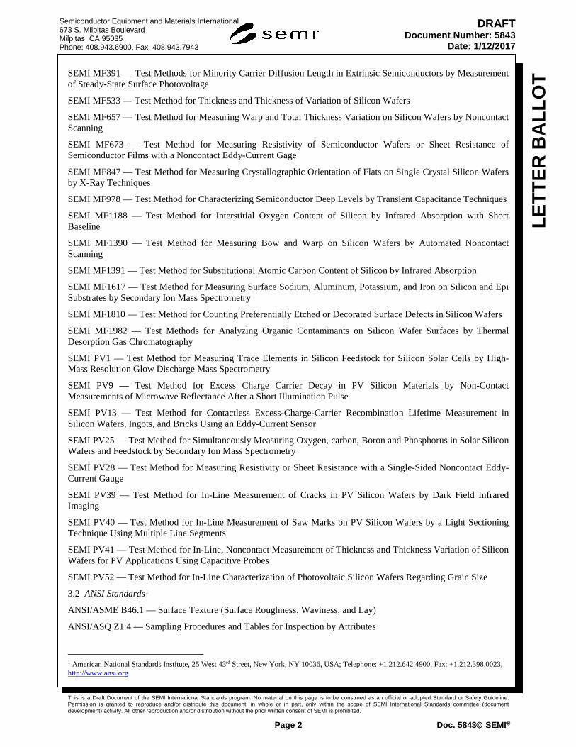
SEMI PV1 — Test Method for Measuring Trace Elements in Silicon Feedstock for Silicon Solar Cells by High-Mass Resolution Glow Discharge Mass Spectrometry
SEMI PV9 — Test Method for Excess Charge Carrier Decay in PV Silicon Materials by Non-Contact Measurements of Microwave Reflectance After a Short Illumination Pulse
SEMI PV13 — Test Method for Contactless Excess-Charge-Carrier Recombination Lifetime Measurement in Silicon Wafers, Ingots, and Bricks Using an Eddy-Current Sensor
SEMI PV25 — Test Method for Simultaneously Measuring Oxygen, carbon, Boron and Phosphorus in Solar Silicon Wafers and Feedstock by Secondary Ion Mass Spectrometry
SEMI PV28 — Test Method for Measuring Resistivity or Sheet Resistance with a Single-Sided Noncontact Eddy-Current Gauge
SEMI PV39 — Test Method for In-Line Measurement of Cracks in PV Silicon Wafers by Dark Field Infrared Imaging
SEMI PV40 — Test Method for In-Line Measurement of Saw Marks on PV Silicon Wafers by a Light Sectioning Technique Using Multiple Line Segments
SEMI PV41 — Test Method for In-Line, Noncontact Measurement of Thickness and Thickness Variation of Silicon Wafers for PV Applications Using Capacitive Probes
SEMI PV52 — Test Method for In-Line Characterization of Photovoltaic Silicon Wafers Regarding Grain Size
3.2 ANSI Standards1
ANSI/ASME B46.1 — Surface Texture (Surface Roughness, Waviness, and Lay)
ANSI/ASQ Z1.4 — Sampling Procedures and Tables for Inspection by Attributes
1 American National Standards Institute, 25 West 43rd Street, New York, NY 10036, USA; Telephone: +1.212.642.4900, Fax: +1.212.398.0023, http://www.ansi.org

This is a Draft Document of the SEMI International Standards program. No material on this page is to be construed as an official or adopted Standard or Safety Guideline. Permission is granted to reproduce and/or distribute this document, in whole or in part, only within the scope of SEMI International Standards committee (document development) activity. All other reproduction and/or distribution without the prior written consent of SEMI is prohibited.
Page 3 Doc. 5843 SEMI
Semiconductor Equipment and Materials International 673 S. Milpitas Boulevard Milpitas, CA 95035 Phone: 408.943.6900, Fax: 408.943.7943
LETT
ER B
ALL
OT
DRAFT Document Number: 5843
Date: 1/12/2017
3.3 ASTM Standards2
ASTM E122 — Standard Practice for Calculating Sample Size to Estimate, With Specified Precision, the Average for a Characteristic of a Lot or Process
3.4 EN Standards3
EN 50513 — Solar Wafers. Data Sheet and Product Information for Crystalline Wafers for Solar Cell Manufacturing
3.5 ISO Standards 4
ISO 14706 — Surface Chemical Analysis – Determination of Surface Elemental Contamination on Silicon Wafers by Total Reflection X-Ray Fluorescence (TXRF) Spectroscopy
3.6 JEITA Standards5
JEITA EM-3501 (18) — Standard Methods for Determining the Orientation of a Semiconductive Silicon Single Crystal
3.7 JIS Standards6
JIS H 0609 — Test Methods of Crystalline Defects in Silicon by Preferential Etch Techniques
JIS H 0611 — Methods of Measurement of Thickness, Thickness Variation and Bow of Silicon Wafer
JIS H 0614 — Visual Inspection for Silicon Wafers with Specular Surfaces
NOTICE: Unless otherwise indicated, all documents cited shall be the latest published versions.
4 Terminology 4.1 Terms and acronyms relating to silicon and other semiconductor technology are defined in SEMIM59.
4.2 Other Acronyms Used in This Standard
4.2.1 µ-PCD — microwave photoconductance decay
4.2.2 GDMS — glow discharge mass spectrometry
4.2.3 LATF — local thickness fluctuations
4.2.4 PV — photovoltaic
4.2.5 QSSPC — quasi steady state photoconductance
4.3 Other Terms Used in This Standard
4.3.1 brick— one or more squared, cropped, and ground sections from an ingot.
4.3.2 cast silicon — crystalline silicon produced by a casting method.
NOTE 1: Wafers cut from cast silicon ingots are typically multicrystalline with grain sizes up to several centimeters, but, depending on the specific casting method used, single crystalline or nearly single crystalline wafer, sometimes called quasi-monocrystalline wafer, may also be obtained.
4.3.3 ingot— a cylindrical or rectangular solid of silicon resulting from a crystallization process, generally of slightly irregular dimensions. 2 ASTM International, 100 Barr Harbor Drive, West Conshohocken, PA 19428-2959, USA; Telephone: +1.610.832.9585, Fax: +1.610.832.9555, http://www.astm.org 3European Committee for Standardization, Avenue Marnix 17, B-1000 Brussels; Telephone: +32.2.5.50.08.11, Fax: +32.2.5.50.08.19, http://www.cen.eu 4 International Organization for Standardization, ISO Central Secretariat, 1, ch. de la Voie-Creuse, CP 56, CH-1211 Geneva 20, Switzerland; Telephone: +41.22.749.01.11, Fax: +41.22.733.34.30, http://www.iso.org 5Japan Electronics and Information Technology Industries Association, Ote Center Building, 1-1-3, Otemachi, Chiyoda-ku, Tokyo 100-0004, Japan; http://www.jeita.or.jp 6 Japanese Standards Association, 4-1-24 Akasaka, Minato-ku, Tokyo 107-8440, Japan; Telephone: +81.3.3583.8005, Fax: +81.3.3586.2014, http://www.jsa.or.jp

This is a Draft Document of the SEMI International Standards program. No material on this page is to be construed as an official or adopted Standard or Safety Guideline. Permission is granted to reproduce and/or distribute this document, in whole or in part, only within the scope of SEMI International Standards committee (document development) activity. All other reproduction and/or distribution without the prior written consent of SEMI is prohibited.
Page 4 Doc. 5843 SEMI
Semiconductor Equipment and Materials International 673 S. Milpitas Boulevard Milpitas, CA 95035 Phone: 408.943.6900, Fax: 408.943.7943
LETT
ER B
ALL
OT
DRAFT Document Number: 5843
Date: 1/12/2017
4.3.4 monocrystalline — a body of crystalline material that contains no large-angle boundaries or twin boundries. (Synonym: single crystal)
4.3.5 multicrystalline — a body of crystalline material that contains large-angle boundaries or twin boundries. Most crystals of this body have dimensions in the millimeter up to centimeter range.
4.3.6 percentage of the largest single grain — the area ratio of the largest grain with the same defined crystallographic orientation to the area of the case silicon wafer, expressed in percent.
5 Ordering Information 5.1 Purchase orders for silicon wafers furnished to this specification shall include the following items. These items are indicated in the Specification Format for Order Entry, Parts 1 and 2, shown in TableA1-1 with a ♦ symbol in the left-most column.
• 2-1.2 Crystallization Method
• 2-1.3 Crystallinity (Single crystal or cast silicon category I, II wafer)
• 2-1.4 Shape (Square or Pseudo-square)
• 2-2.1 Nominal Size
• 2-2.3 Average Thickness
• 2-2.4 Average Thickness Tolerance
• 2-3.1 Conductivity Type
• 2-3.2 Dopant
• 2-3.3 Bulk Resistivity or Sheet Resistance
• 2-3.4 Location of Resistivity Measurement
• 2-3.5 Effective Minority Carrier Lifetime
• 2-4.1 Oxygen Concentration
• 2-4.2 Carbon Concentration
• 2-4.3 Bulk Iron Content
• 2-5.1 Dislocation Etch Pit Density (required for single crystal wafers only)
• 2-5.2 Crystallographic Orientation (required for single crystal wafers only)
• 2-5.3 Edge Orientation (required for single crystal wafers only)
• 2-5.4 The percentage of the largest single grain (required for cast silicon wafers only)
• 2-5.5 Orientation of the largest single grain (required for cast silicon wafers only)
5.2 In addition, the purchase order must indicate the test method to be used in evaluating each of those items for which alternate test procedures exist.
5.3 The following items must also be included in the purchase order:
5.3.1 Lot acceptance procedures (see ¶7.2),
5.3.2 Certification (if required) (see §9),
5.3.3 Packing and marking (see §10),
5.4 Optional Criteria — Any of the remainder of the items listed in TableA1-1 may be specified optionally in addition to those listed above:
5.5 In all cases, it is essential that all choices for the items included in the purchase order be made in order not to have undefined parameters that would lead to surprises between supplier and customer.
This is a Draft Document of the SEMI International Standards program. No material on this page is to be construed as an official or adopted Standard or Safety Guideline. Permission is granted to reproduce and/or distribute this document, in whole or in part, only within the scope of SEMI International Standards committee (document development) activity. All other reproduction and/or distribution without the prior written consent of SEMI is prohibited.
Page 5 Doc. 5843 SEMI
Semiconductor Equipment and Materials International 673 S. Milpitas Boulevard Milpitas, CA 95035 Phone: 408.943.6900, Fax: 408.943.7943
LETT
ER B
ALL
OT
DRAFT Document Number: 5843
Date: 1/12/2017
6 Requirements 6.1 General Characteristics
6.1.1 The crystallization method shall be as specified on the purchase order.
6.1.2 The crystallinity of the wafer shall be specified as either single crystal or cast silicon category I, II wafer.
6.1.3 The shape of the finished wafer shall be specified as square or pseudo-square.
6.2 Dimensions and Permissible Variations
6.2.1 Wafer Thickness and Thickness Variation
6.2.1.1 The center point wafer thickness shall be specified.
6.2.1.2 The variation of center point thickness of wafers in a lot shall be less than 5% (or other specified fraction) of the specified wafer thickness.
6.2.1.3 The total thickness variation within a wafer shall be specified.
6.2.2 Square Wafer Dimensions
6.2.2.1 Square wafers have straight chamfers at the corners. The typical chamfer angle α, between the wafer edge and the straight chamfer is 45°, but there is no specification for this angle.
6.2.2.2 The allowable dimensions of square wafers are indicated in Figure1 and Table1.
6.2.2.3 The specified dimensions are the wafer edge lengths, A, the diagonal, G (to insure squareness of the wafer edges), and the chamfer width, H. All dimensions are given in millimeters. Other dimensions in Figure1 can be calculated from the specified dimensions using ordinary trigonometric functions.
6.2.2.4 Dimension H is specified to be identical for all sizes, but by agreement between supplier and customer, one of the four corner chamfers can be of different size to indicate the orientation of the wafer.
6.2.2.5 TTV— For all wafer sizes, the maximum TTV shall not exceed 30 µm (or other specified amount).
6.2.2.6 Warp — For all sizes of square wafers, the maximum warp shall not exceed 75 µm (or other specified amount).
NOTE 2: The areas of square wafers are given for information in Related Information1.
6.2.3 Pseudo-Square Single Crystal Wafer Dimensions
6.2.3.1 Pseudo-square wafers are cut from a circular single-crystal boule and have round chamfers at the corners.
6.2.3.2 The allowable dimensions of pseudo-square single crystal wafers are indicated in Figure2 and Table2. These wafers have rounded chamfers of equal size on all four corners.
6.2.3.3 The specified dimensions are the wafer edge length, A, the diameter, D, and the chamfer distance, F, which is the length of a leg of a right isosceles triangle. Because F is the same for all corners, the center of the square of dimension A is the same as the center of the circle of diameter D. All dimensions are given in millimeters. The dimension, C, also shown in Figure2 can be calculated as the length A – 2F.

This is a Draft Document of the SEMI International Standards program. No material on this page is to be construed as an official or adopted Standard or Safety Guideline. Permission is granted to reproduce and/or distribute this document, in whole or in part, only within the scope of SEMI International Standards committee (document development) activity. All other reproduction and/or distribution without the prior written consent of SEMI is prohibited.
Page 6 Doc. 5843 SEMI
Semiconductor Equipment and Materials International 673 S. Milpitas Boulevard Milpitas, CA 95035 Phone: 408.943.6900, Fax: 408.943.7943
LETT
ER B
ALL
OT
DRAFT Document Number: 5843
Date: 1/12/2017
α
A C
A G
E
G
H
Figure 1
Dimensions of Square Single Crystal Silicon Wafers for PV Solar Cell Applications Table 1 Dimensions of Square Silicon Wafers for PV Solar Cell Applications
Dimensions
Symbol in Figure 1#1 A (mm) G (mm) H (mm)
Dimension Name Wafer Edge Length Diagonal Chamfer Length
Nominal Size (mm) Max Min Max Min Max Min
100 101 99 142.8 140.0 2 0.5 125 126 124 178.2 175.4 2 0.5 156 157 155 222.0 219.2 2 0.5 210 211 209 298.4 295.6 2 0.5
Symbol in EN50513 A, B C H Symbol in SEMIM6 A, B C D
Symbol in Figure 1#1 Dimensions
Dimension Name A (mm)
Wafer Edge Length G (mm)
Diagonal H (mm)
Chamfer Length
Nominal Size (mm)
100.75 100.75±0.25 142.4±0.5 1.25±0.75
125.75 125.75±0.25 177.8±0.5 1.25±0.75
156.75 156.75±0.25 221.6±0.5 1.25±0.75
210.75 210.75±0.25 298.0±0.5 1.25±0.75
Symbol in EN 50513 A, B C H Symbol in SEMI M6 A, B C D
#1 The letter symbols in Figure1 differ as indicated from those in both the previous SEMI Specification for silicon wafers for solar cell application (SEMI M6, now superseded by this Standard), and EN 50513. Note that both SEMI M6 and EN 50513 used a different symbol for
This is a Draft Document of the SEMI International Standards program. No material on this page is to be construed as an official or adopted Standard or Safety Guideline. Permission is granted to reproduce and/or distribute this document, in whole or in part, only within the scope of SEMI International Standards committee (document development) activity. All other reproduction and/or distribution without the prior written consent of SEMI is prohibited.
Page 7 Doc. 5843 SEMI
Semiconductor Equipment and Materials International 673 S. Milpitas Boulevard Milpitas, CA 95035 Phone: 408.943.6900, Fax: 408.943.7943
LETT
ER B
ALL
OT
DRAFT Document Number: 5843
Date: 1/12/2017
each of the two wafer edge lengths. The dimensions shown in Figure 1 by C, E, and α do not appear in SEMI M6. The dimension E is taken from EN 50513, but values are not specified here because they are determined from the combination of G, and H.
6.2.3.4 TTV — For all sizes of pseudo-square wafers, the maximum TTV shall not exceed 30µm (or other specified amount).
6.2.3.5 Warp — For all sizes of pseudo-square wafers, the maximum warp shall not exceed 75µm (or other specified amount).
NOTE 3: The areas of pseudo-square wafers are given for information in Related Information1.
6.3 Materials and Manufacture
6.3.1 The material shall consist of wafers conforming to the crystallinity class specified in the purchase order or contract.
6.4 Electrical Parameters
6.4.1 The material shall conform to the details specified in the purchase order or contract, as follows:
6.4.1.1 Conductivity type and dopant,
6.4.1.2 Resistivity,
6.4.1.3 Diffusion length or effective minority carrier lifetime.
6.5 Chemical Characteristics
6.5.1 The material shall conform to the interstitial or total oxygen content, the substitutional or total carbon content, and bulk iron content as specified in the purchase order or contract.
6.5.2 In addition, the content of one or more individual metals and/or total metal content may optionally be required. In each case, the metal(s) to be determined shall be identified.
6.6 Crystal Characteristics
6.6.1 Single crystal wafers shall conform to the maximum dislocation etch pit density and crystal and edge orientation as specified in the purchase order or contract.
6.6.2 The percentage of the largest single grain — Cast silicon wafers shall be categorized by the percentage of the largest single grain as defined in Table 1. Categories I and II differ in the percentage of the largest single grain. Table 2 Percentage of the Largest Single Grain of Cast Silicon Wafer
Item#1 Cast Silicon Category I Cast Silicon Category II
The percentage of the largest single grain ≥85% <85%
#1 For cast silicon category I wafers which can be treated by anisotropic texturing (e.g., alkaline solution) to gain the well textured surface of low reflectance, instead of isotropic texturing for the traditional cast silicon category II.
6.7 Wafer Defect Limits — Wafers shall conform to the defect limits as specified in the purchase order or contract.

This is a Draft Document of the SEMI International Standards program. No material on this page is to be construed as an official or adopted Standard or Safety Guideline. Permission is granted to reproduce and/or distribute this document, in whole or in part, only within the scope of SEMI International Standards committee (document development) activity. All other reproduction and/or distribution without the prior written consent of SEMI is prohibited.
Page 8 Doc. 5843 SEMI
Semiconductor Equipment and Materials International 673 S. Milpitas Boulevard Milpitas, CA 95035 Phone: 408.943.6900, Fax: 408.943.7943
LETT
ER B
ALL
OT
DRAFT Document Number: 5843
Date: 1/12/2017
Figure 2
Dimensions of Pseudo-Square Single Crystal Silicon Wafers for PV Solar Cell Applications Table 3 Dimensions of Pseudo-Square Silicon Wafers for PV Solar Cell Applications
Dimensions (mm)
Symbol in Figure 2#1 A D
Dimension Name Wafer Edge Length Diameter
Nominal Size (mm) Maximum Minimum Maximum Minimum
100 101 99 126 124 125 126 124 151 149 156 157 155 206 204 210 211 209 291 289
Symbol in EN 50513 A E Symbol in SEMI M6 A B
Symbol in Figure 2#1 Dimensions (mm)
Dimension Name A (mm)
Wafer Edge Length D (mm)
Diameter
Nominal Size (mm)
100.75 100.75±0.25 126±0.25 125.75 125.75±0.25 151±0.25
156Ⅰ 156.75±0.25 205±0.25
156Ⅱ 156.75±0.25 210±0.25 210.75 210.75±0.25 291±0.25
Symbol in EN 50513 A E Symbol in SEMI M6 A B
#2 The letter symbols in Figure 2 differ as indicated from those in both the previous SEMI Specification for silicon wafers for solar cell application (SEMIM6, now superseded by this Standard), and EN50513. Note that the dimensions C and F, which are shown in Figure2, are not listed in the dimension table because these two dimensions can be simply calculated from the edge length and diameter.

This is a Draft Document of the SEMI International Standards program. No material on this page is to be construed as an official or adopted Standard or Safety Guideline. Permission is granted to reproduce and/or distribute this document, in whole or in part, only within the scope of SEMI International Standards committee (document development) activity. All other reproduction and/or distribution without the prior written consent of SEMI is prohibited.
Page 9 Doc. 5843 SEMI
Semiconductor Equipment and Materials International 673 S. Milpitas Boulevard Milpitas, CA 95035 Phone: 408.943.6900, Fax: 408.943.7943
LETT
ER B
ALL
OT
DRAFT Document Number: 5843
Date: 1/12/2017
7 Sampling 7.1 Unless otherwise specified, ASTME122 shall be used.
7.1.1 When so specified, the appropriate sample sizes shall be selected from each lot in accordance with ANSI/ASQ Z1.4. Each quality characteristic shall be assigned an acceptable quality level (AQL) and lot tolerance percent defective (LTPD) value in accordance with the ANSI/ASQ Z1.4 definitions for critical, major, and minor classifications. If desired and so specified in the contract or order, each of these classifications may alternatively be assigned cumulative AQL and LTPD values. Inspection levels shall be agreed upon between the supplier and the customer.
7.2 For the purposes of this Specification, a lot is either (a) all of the wafers of nominally identical size and characteristics contained in a single shipment, or (b) subdivisions of large shipments consisting of wafers as listed above that have been identified by the supplier as constituting a lot.
8 Test Methods NOTE 4: Silicon wafers are extremely fragile. While the mechanical dimensions of a wafer can be measured by use of tools such as micrometer calipers and other conventional techniques, the wafer may be damaged physically in ways that are not immediately evident. Special care must therefore be used in the selection and execution of measurement methods.
8.1 Dimensional Characteristics
8.1.1 Length, Width, or Diameter— Determine the edge length of rectangular and pseudo-square wafers by a method agreed upon between the supplier and the purchaser.
8.1.2 Center Point Thickness and Total Thickness Variation (TTV) — Make these measurements with contact or non-contact equipment as agreed by supplier and purchaser. It should be noted that measurements with contact equipment are not likely to give the same result as those with non-contact equipment because of the effects of surface roughness of the test specimen.
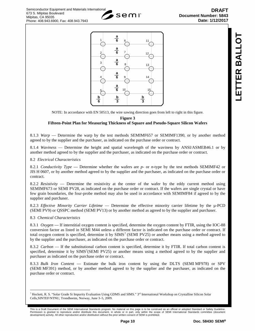
8.1.2.1 Determine the center point thickness by the test methods SEMIMF533, SEMI PV41 or JISH0611 or by using point 8 of the 15-point pattern given in EN50514, as indicated on the purchase order or contract. The full 15-point pattern is reproduced in Figure3.
8.1.2.2 Determine TTV by the test methods SEMIMF533, SEMI PV41 or JISH0611, by using points 1, 5, 8, 11, and 15 of the 15-point pattern, by using all points in the 15-point pattern, or by another method agreed to by the supplier and the purchaser, as indicated on the purchase order or contract.
This is a Draft Document of the SEMI International Standards program. No material on this page is to be construed as an official or adopted Standard or Safety Guideline. Permission is granted to reproduce and/or distribute this document, in whole or in part, only within the scope of SEMI International Standards committee (document development) activity. All other reproduction and/or distribution without the prior written consent of SEMI is prohibited.
Page 10 Doc. 5843 SEMI
Semiconductor Equipment and Materials International 673 S. Milpitas Boulevard Milpitas, CA 95035 Phone: 408.943.6900, Fax: 408.943.7943
LETT
ER B
ALL
OT
DRAFT Document Number: 5843
Date: 1/12/2017
a 6
a 6
a 6
a 6
a 6
b 6
b 3
b 3
3
1
2
4
5
6
8
9
10
7
11
15
12
13
14
NOTE: In accordance with EN 50513, the wire sawing direction goes from left to right in this figure.
Figure 3 Fifteen-Point Plan for Measuring Thickness of Square and Pseudo-Square Silicon Wafers
8.1.3 Warp — Determine the warp by the test methods SEMIMF657 or SEMIMF1390, or by another method agreed to by the supplier and the purchaser, as indicated on the purchase order or contract.
8.1.4 Waviness — Determine the height and spatial wavelength of the waviness by ANSI/ASMEB46.1 or by another method agreed to by the supplier and the purchaser, as indicated on the purchase order or contract.
8.2 Electrical Characteristics
8.2.1 Conductivity Type — Determine whether the wafers are p- or n-type by the test methods SEMIMF42 or JIS H 0607, or by another method agreed to by the supplier and the purchaser, as indicated on the purchase order or contract.
8.2.2 Resistivity — Determine the resistivity at the center of the wafer by the eddy current method using SEMIMF673 or SEMI PV28, as indicated on the purchase order or contract. If the wafers are single crystal or have few grain boundaries, the four-probe method may also be used in accordance with SEMIMF84 if agreed to by the supplier and purchaser.
8.2.3 Effective Minority Carrier Lifetime — Determine the effective minority carrier lifetime by the µ-PCD (SEMI PV9) or QSSPC method (SEMI PV13) or by another method as agreed to by the supplier and purchaser.
8.3 Chemical Characteristics
8.3.1 Oxygen — If interstitial oxygen content is specified, determine the oxygen content by FTIR, using the IOC-88 conversion factor as listed in SEMI M44 unless a different factor is indicated on the purchase order or contract. If total oxygen content is specified, determine it by SIMS7 (SEMI PV25) or another means using a method agreed to by the supplier and the purchaser, as indicated on the purchase order or contract.
8.3.2 Carbon — If the substitutional carbon content is specified, determine it by FTIR. If total carbon content is specified, determine it by SIMS7(SEMI PV25) or another means using a method agreed to by the supplier and purchaser as indicated on the purchase order or contract.
8.3.3 Bulk Iron Content — Estimate the bulk iron content by using the DLTS (SEMI MF978) or SPV (SEMI MF391) method, or by another method agreed to by the supplier and the purchaser, as indicated on the purchase order or contract.
7 Hockett, R. S. “Solar Grade Si Impurity Evaluation Using GDMS and SIMS.” 3rd International Workshop on Crystalline Silicon Solar Cells,SINTEF/NTNU, Trondheeim, Norway, June 3–5, 2009.

This is a Draft Document of the SEMI International Standards program. No material on this page is to be construed as an official or adopted Standard or Safety Guideline. Permission is granted to reproduce and/or distribute this document, in whole or in part, only within the scope of SEMI International Standards committee (document development) activity. All other reproduction and/or distribution without the prior written consent of SEMI is prohibited.
Page 11 Doc. 5843 SEMI
Semiconductor Equipment and Materials International 673 S. Milpitas Boulevard Milpitas, CA 95035 Phone: 408.943.6900, Fax: 408.943.7943
LETT
ER B
ALL
OT
DRAFT Document Number: 5843
Date: 1/12/2017
8.3.4 Other Metal Content — Determine the content of other specified metal(s) by GDMS (SEMIPV1), or by SIMS7(SEMI PV25) or by another method agreed to by the supplier and the purchaser, as indicated on the purchase order or contract.
8.3.5 Total Metal Content — List the metals to be tested and determine the total metal content by GDMS (SEMIPV1), or by SIMS or by another method agreed to by the supplier and the purchaser, as indicated on the purchase order or contract.
8.4 Crystal Characteristics of Crystalline Silicon Wafers
8.4.1 Dislocation Etch Pit Density — For single crystal silicon wafers, determine the etch pit density on the surface of the wafer by SEMIMF1809 or JIS H 0609, or by another method agreed to by the supplier and the purchaser, as indicated on the purchase order or contract.
8.4.2 Surface Orientation— For single crystal silicon wafers, determine in accordance with SEMIMF26, or by another method agreed to by the supplier and the purchaser, as indicated on the purchase order or contract.
8.4.3 Edge Orientation — For single crystal silicon wafers, determine by the flat orientation method of SEMIMF847, or by another method agreed to by the supplier and the purchaser, if this measurement is required on the purchase order or contract.
8.4.4 The Percentage of the Largest Single Grain — For cast silicon wafers, determine the percentage of the largest single grain with SEMI PV52 or by another method agreed to by the supplier and the purchaser as indicated on the purchase order or contract.
8.4.5 Orientation of the Largest Single Grain — For cast silicon wafers, determine in accordance with SEMI MF26, or by another method agreed to by the supplier and the purchaser, as indicated on the purchase order or contract.
8.5 Surface and Edge Inspection Characteristics
8.5.1 Area Contamination — Determine by visual inspection in accordance with SEMI MF523 or JIS H 0614 or by SSIS, or by another method agreed to by the supplier and the purchaser, as indicated on the purchase order or contract.
8.5.2 Nonvisible Contamination — Determine by corrosion rate measurement in accordance with §12 of EN 50513, or by another method agreed to by the supplier and the purchaser, as indicated on the purchase order or contract.
8.5.3 Cracks — Determine by visual inspection in accordance with SEMIMF523, SEMI PV39 or JIS H 0614 or by SSIS, or by another method agreed to by the supplier and the purchaser, as indicated on the purchase order or contract.
8.5.4 Edge Breakage — Determine non V-type indents at the edge by visual inspection in accordance with SEMI MF523 or JIS H 0614 or by SSIS, or by another method agreed to by the supplier and the purchaser, as indicated on the purchase order or contract.
8.5.5 Edge Chips — Determine by corrosion rate measurement in accordance with §12 of EN 50513, or by another method agreed to by the supplier and the purchaser, as indicated on the purchase order or contract.
8.5.6 Edge Crown — Determine the maximum difference between the surface elevation at 3.2mm from the edge of the wafer and the elevation at the wafer edge in accordance with DIN50446, or by another method agreed to by the supplier and the purchaser, as indicated on the purchase order or contract.
8.5.7 Edge Deviation — Determine the minimum spatial wavelength and the maximum deviation from a curve fitted to the edge of the wafer by a method agreed to by the supplier and the purchaser, as indicated on the purchase order or contract.
8.5.8 Inclusions — Determine the dimensions and number of visible inclusions in the silicon matrix that affect the electrical, optical, or chemical properties of the wafer by visual inspection in accordance with SEMIMF523 or JIS H 0614, or by another method agreed to by the supplier and the purchaser, as indicated on the purchase order or contract.
8.5.9 Pits — Determine the depth, width, and number of pits on the wafers surface visually by using SEMIMF523 or JIS H 0614 or by SSIS, or by another method agreed to by the supplier and the purchaser, as indicated on the purchase order or contract.

This is a Draft Document of the SEMI International Standards program. No material on this page is to be construed as an official or adopted Standard or Safety Guideline. Permission is granted to reproduce and/or distribute this document, in whole or in part, only within the scope of SEMI International Standards committee (document development) activity. All other reproduction and/or distribution without the prior written consent of SEMI is prohibited.
Page 12 Doc. 5843 SEMI
Semiconductor Equipment and Materials International 673 S. Milpitas Boulevard Milpitas, CA 95035 Phone: 408.943.6900, Fax: 408.943.7943
LETT
ER B
ALL
OT
DRAFT Document Number: 5843
Date: 1/12/2017
8.5.10 Surface Roughness—Determine the surface roughness by a BRDF method or by AFM or by another method agreed to by the supplier and the purchaser, as indicated on the purchase order or contract.
8.5.11 Groove-type Saw Marks — Determine the depth and number of grooves in accordance with DIN 4774 or ANSI/ASME B46.1, or by another method agreed to by the supplier and the purchaser, as indicated on the purchase order or contract.
8.5.12 Step-type Saw Marks — Determine the depth and number of steps in accordance with DIN 4774 or ANSI/ASME B46.1, or by another method agreed to by the supplier and the purchaser, as indicated on the purchase order or contract.
8.5.13 Surface Chips — Determine by visual inspection in accordance with SEMI MF523 or JIS H 0614 or by SSIS, or by another method agreed to by the supplier and the purchaser, as indicated on the purchase order or contract.
8.5.14 V-chips — Determine by visual inspection in accordance with SEMI MF523 or JIS H 0614 or by SSIS, or by another method agreed to by the supplier and the purchaser, as indicated on the purchase order or contract.
8.5.15 Surface Metal Contamination— Determine the concentration of specified metal contaminants by ICP/MS. AAS, SIMS (SEMI PV25) in accordance with SEMIMF1617, TXRF in accordance with ISO14706, or by another method agreed to by the supplier and the purchaser as indicated on the purchase order or contract.
8.5.16 Surface Organics— Determine the density of surface organics in accordance with SEMIMF1982 or by another method agreed to by the supplier and the purchaser as indicated on the purchase order or contract.
9 Certification 9.1 Upon request of the purchaser in the contract or order, a manufacturer’s or supplier’s certification that the material was manufactured and tested in accordance with this Specification, together with a report of the test results, shall be furnished at the time of shipment.
9.2 In the interest of controlling inspection costs, the supplier and the purchaser may agree that the material shall be certified as ‘capable of meeting’ certain requirements. In this context, ‘capable of meeting’ shall signify that the supplier is not required to perform the appropriate tests in §8. However, if the purchaser performs the test and the material fails to meet the requirement, the material may be subject to rejection.
10 Packing and Package Labeling 10.1 Special packing requirements shall be subject to agreement between the supplier and the purchaser. Otherwise all wafers shall be handled, inspected, and packed in such a manner as to avoid chipping, scratches, and contamination, and in accordance with the best industry practices to provide ample protection against damage during shipment.
10.2 The wafers supplied under these specifications shall be identified by appropriately labeling the outside of each box or other container and each subdivision thereof in which it may reasonably be expected that the wafers will be stored prior to further processing. Identification shall include as a minimum the nominal diameter, conductivity type, dopant, orientation, resistivity range, and lot number. The lot number, either (1) assigned by the original manufacturer of the wafers, or (2) assigned subsequent to wafer manufacture but providing reference to the original lot number, shall provide easy access to information concerning the fabrication history of the particular wafers in that lot. Such information shall be retained on file at the manufacturer’s facility for at least one year after that particular lot has been accepted by the purchaser.
11 Related Documents 11.1 The following DIN standards no longer seem to be active on the DIN Web site (http://www.din.de) so they have been removed from §3 and listed here for historical reference.
DIN 4774 — Measurement of Wave Depth with Electrical Contact Stylus Instruments
DIN 50431 — Measurement of the Electrical Resistivity of Silicon or Germanium Single Crystals by Means of the Four-Point-Probe Direct Current method with collinear Four Probe Array
DIN 50432 — Determination of the Conductivity Type of Silicon or Germanium by Means of Rectification Test or Hot-Probe

This is a Draft Document of the SEMI International Standards program. No material on this page is to be construed as an official or adopted Standard or Safety Guideline. Permission is granted to reproduce and/or distribute this document, in whole or in part, only within the scope of SEMI International Standards committee (document development) activity. All other reproduction and/or distribution without the prior written consent of SEMI is prohibited.
Page 13 Doc. 5843 SEMI
Semiconductor Equipment and Materials International 673 S. Milpitas Boulevard Milpitas, CA 95035 Phone: 408.943.6900, Fax: 408.943.7943
LETT
ER B
ALL
OT
DRAFT Document Number: 5843
Date: 1/12/2017
DIN 50433-1 — Determining the Orientation of Single Crystals by Means of X-Ray Diffraction
DIN 50433-2 — Determining the Orientation of Single Crystals by Means of Optical Reflection Figure
DIN 50433-3 — Determination of the Orientation of Single Crystals by Means of Laue Back Scattering
DIN 50434 — Determination of Crystal Defects in Monocrystalline Silicon Using Etching Techniques on {111} and {100} Surfaces
DIN 50438-1 — Determination of Impurity Content in Silicon by Infrared Absorption – Oxygen
DIN 50438-2 — Determination of Impurity Content in Silicon by infrared Absorption – Carbon
DIN 50441-1 — Determination of the Geometric Dimensions of Semiconductor Wafers; Part 1: Measurement of Thickness
DIN 50443-1 — Recognition of Defects and in homogeneities in Semiconductor Single Crystals by X-Ray Topography: Silicon
DIN 50445 — Contactless Determination of the Electrical Resistivity of Semiconductor Wafers with the Eddy Current Method
DIN 50446 — Determining Types and Densities of Defects in Silicon Epitaxial Layers

This is a Draft Document of the SEMI International Standards program. No material on this page is to be construed as an official or adopted Standard or Safety Guideline. Permission is granted to reproduce and/or distribute this document, in whole or in part, only within the scope of SEMI International Standards committee (document development) activity. All other reproduction and/or distribution without the prior written consent of SEMI is prohibited.
Page 14 Doc. 5843 SEMI
Semiconductor Equipment and Materials International 673 S. Milpitas Boulevard Milpitas, CA 95035 Phone: 408.943.6900, Fax: 408.943.7943
LETT
ER B
ALL
OT
DRAFT Document Number: 5843
Date: 1/12/2017
APPENDIX 1 SPECIFICATION FORMAT FOR ORDER ENTRY NOTICE: The material in this Appendix is an official part of SEMI PV22 and was approved by full letter ballot procedures on September 12, 2011.
A1-1 Specification Format A1-1.1 The listing in the format for order entry in TableA1-1 provides a systematic basis for constructing the purchase order for any kind of crystalline silicon wafers for photovoltaic applications. Both standardized and non-standardized properties are included in the format together with appropriate test methodology for verifying these properties.
A1-1.2 Consequently, this Standard can be used both for characterizing standardized material and advanced material for development and extension of present PV technologies.
A1-1.3 It may or may not be that in the future additional properties could be standardized, but inclusion in this table does not mean that such properties are expected to become standards. Table A1-1 Specification Format for Order Entry Part 1 General Information
ITEM INFORMATION Date:
Customer Name Purchase Order Number Line Number Item Number General Specification Number Revision Level Part Number/Revision
Part 2 Crystalline Silicon Wafers for Photovoltaic Solar Cells
ITEM SPECIFICATION MEASUREMENT METHOD
2-1 GENERAL CHARACTERISTICS#1 2-1.1 Source Material [ ] Virgin poly silicon;
[ ] Other: (specify)__________; [ ] Not specified
♦ 2-1.2 Crystallization Method [ ] Cz; [ ] Bridgman; [ ] Ingot Casting; [ ] Directional Solidification; [ ] Float Zone; [ ] Other: (specify)__________
♦ 2-1.3 Crystallinity [ ] Single crystal; [ ] Cast silicon category I; [ ] Cast silicon category II
♦ 2-1.4 Shape [ ] Square [ ]; Pseudo-square#2
2-2 DIMENSIONAL CHARACTERISTICS#1 ♦ 2-2.1 Nominal Size#3 [ ] 100.75 mm; [ ] 125.75 mm; [ ] 156.75 mm; [ ]
156Ⅰmm; [ ] 156Ⅱmm;[ ] 210.75 mm;[ ] 100 mm; [ ] 125 mm; [ ] 156 mm; [ ] 210 mm
2-2.1.1 Other Size [ ] A: ____±____ mm; [ ] G or [ ] D: ____±____ mm
2-2.2 Chamfer Angle [ ] 45 ± ____°; [ ] Other: (specify) __________ [ ] Not specified
[ ] Optical microscope; [ ] Projected image; [ ] Other: (specify) __________
This is a Draft Document of the SEMI International Standards program. No material on this page is to be construed as an official or adopted Standard or Safety Guideline. Permission is granted to reproduce and/or distribute this document, in whole or in part, only within the scope of SEMI International Standards committee (document development) activity. All other reproduction and/or distribution without the prior written consent of SEMI is prohibited.
Page 15 Doc. 5843 SEMI
Semiconductor Equipment and Materials International 673 S. Milpitas Boulevard Milpitas, CA 95035 Phone: 408.943.6900, Fax: 408.943.7943
LETT
ER B
ALL
OT
DRAFT Document Number: 5843
Date: 1/12/2017
ITEM SPECIFICATION MEASUREMENT METHOD
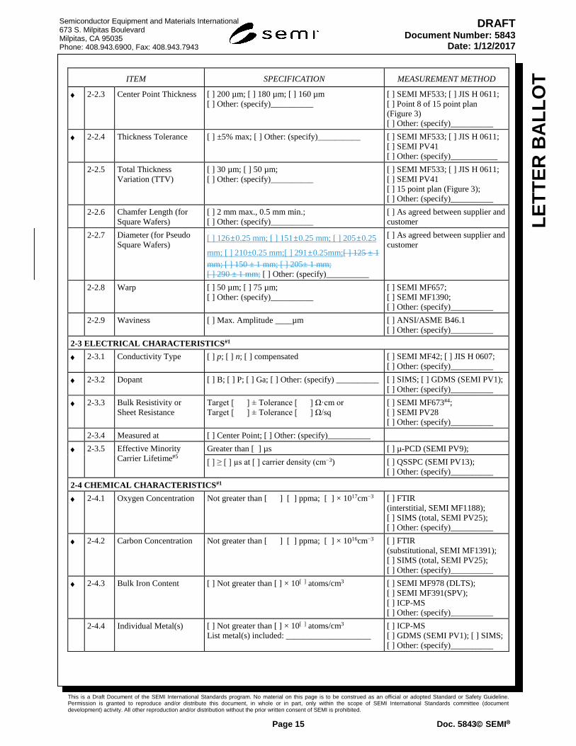
♦ 2-2.3 Center Point Thickness [ ] 200 µm; [ ] 180 µm; [ ] 160 µm [ ] Other: (specify)__________
[ ] SEMI MF533; [ ] JIS H 0611; [ ] Point 8 of 15 point plan (Figure 3) [ ] Other: (specify)__________
♦ 2-2.4 Thickness Tolerance [ ] ±5% max; [ ] Other: (specify)__________ [ ] SEMI MF533; [ ] JIS H 0611; [ ] SEMI PV41 [ ] Other: (specify)___________
2-2.5 Total Thickness Variation (TTV)
[ ] 30 µm; [ ] 50 µm; [ ] Other: (specify)__________
[ ] SEMI MF533; [ ] JIS H 0611; [ ] SEMI PV41 [ ] 15 point plan (Figure 3); [ ] Other: (specify)__________
2-2.6 Chamfer Length (for Square Wafers)
[ ] 2 mm max., 0.5 mm min.; [ ] Other: (specify)__________
[ ] As agreed between supplier and customer
2-2.7 Diameter (for Pseudo Square Wafers)
[ ] 126±0.25 mm; [ ] 151±0.25 mm; [ ] 205±0.25
mm; [ ] 210±0.25 mm;[ ] 291±0.25mm;[ ] 125 ± 1 mm; [ ] 150 ± 1 mm; [ ] 205± 1 mm; [ ] 290 ± 1 mm; [ ] Other: (specify)__________
[ ] As agreed between supplier and customer
2-2.8 Warp [ ] 50 µm; [ ] 75 µm; [ ] Other: (specify)__________
[ ] SEMI MF657; [ ] SEMI MF1390; [ ] Other: (specify)__________
2-2.9 Waviness [ ] Max. Amplitude ____µm [ ] ANSI/ASME B46.1 [ ] Other: (specify)__________
2-3 ELECTRICAL CHARACTERISTICS#1 ♦ 2-3.1 Conductivity Type [ ] p; [ ] n; [ ] compensated [ ] SEMI MF42; [ ] JIS H 0607;
[ ] Other: (specify)__________
♦ 2-3.2 Dopant [ ] B; [ ] P; [ ] Ga; [ ] Other: (specify) __________ [ ] SIMS; [ ] GDMS (SEMI PV1); [ ] Other: (specify)__________
♦ 2-3.3 Bulk Resistivity or Sheet Resistance
Target [ ] ± Tolerance [ ] Ω·cm or Target [ ] ± Tolerance [ ] Ω/sq
[ ] SEMI MF673#4; [ ] SEMI PV28 [ ] Other: (specify)__________
2-3.4 Measured at [ ] Center Point; [ ] Other: (specify)__________ ♦ 2-3.5 Effective Minority
Carrier Lifetime#5 Greater than [ ] µs [ ] µ-PCD (SEMI PV9); [ ] ≥ [ ] µs at [ ] carrier density (cm−3) [ ] QSSPC (SEMI PV13);
[ ] Other: (specify)__________ 2-4 CHEMICAL CHARACTERISTICS#1 ♦ 2-4.1 Oxygen Concentration Not greater than [ ] [ ] ppma; [ ] × 1017cm−3 [ ] FTIR
(interstitial, SEMI MF1188); [ ] SIMS (total, SEMI PV25); [ ] Other: (specify)__________
♦ 2-4.2 Carbon Concentration Not greater than [ ] [ ] ppma; [ ] × 1016cm−3 [ ] FTIR (substitutional, SEMI MF1391); [ ] SIMS (total, SEMI PV25); [ ] Other: (specify)__________
♦ 2-4.3 Bulk Iron Content [ ] Not greater than [ ] × 10[ ] atoms/cm3 [ ] SEMI MF978 (DLTS); [ ] SEMI MF391(SPV); [ ] ICP-MS [ ] Other: (specify)__________
2-4.4 Individual Metal(s) [ ] Not greater than [ ] × 10[ ] atoms/cm3
List metal(s) included: ____________________ [ ] ICP-MS [ ] GDMS (SEMI PV1); [ ] SIMS; [ ] Other: (specify)__________

This is a Draft Document of the SEMI International Standards program. No material on this page is to be construed as an official or adopted Standard or Safety Guideline. Permission is granted to reproduce and/or distribute this document, in whole or in part, only within the scope of SEMI International Standards committee (document development) activity. All other reproduction and/or distribution without the prior written consent of SEMI is prohibited.
Page 16 Doc. 5843 SEMI
Semiconductor Equipment and Materials International 673 S. Milpitas Boulevard Milpitas, CA 95035 Phone: 408.943.6900, Fax: 408.943.7943
LETT
ER B
ALL
OT
DRAFT Document Number: 5843
Date: 1/12/2017
ITEM SPECIFICATION MEASUREMENT METHOD
2-4.5 Total Metal Content [ ] Not greater than [ ] × 10[ ] atoms/cm3 List metals included: _____________________
[ ] ICP-MS [ ] GDMS (SEMI PV1); [ ] SIMS; [ ] Other: (specify)__________
2-5 CRYSTAL CHARACTERISTICS#6 2-5.1 Dislocation Etch Pit
Density [ ] Not greater than [ ]/cm2 [ ] SEMI MF1810; [ ] JIS H 0609;
[ ] Other: (specify)__________ 2-5.2 Crystallographic
Orientation [ ] (100); [ ] (111); [ ] (110); [ ] Other: (specify) ( )
[ ] SEMI MF26 (X-Ray); [ ] SEMI MF26 (Optical); [ ] JEITA EM-3501; [ ] DIN 50433/3; [ ] Other: (specify)__________
2-5.3 Edge Orientation [ ] (crystal axis) [_____] ± ____° [ ] SEMI MF847 (Flat); [ ] Other: (specify)__________
♦ 2-5.4 The percentage of the largest single grain
[ ] Category I,≥85% [ ] Category II, <85%; [ ] Other: (specify)__________
[ ] SEMI PV52; [ ] Other: (specify)__________
2-5.5 Orientation of the largest single grain
[ ] (100); [ ] Other: (specify) ( ) [ ] SEMI MF26; [ ] Other: (specify)__________
2-5.6 Orientation tolerance of the largest single grain
[ ]±5 degrees; [ ] Other: (specify)__________ [ ] SEMI MF26; [ ] Other: (specify)__________
2-6 SURFACE AND EDGE INSPECTION CHARACTERISTICS 2-6.1 Contamination, Area
(Visible to Naked Eye under Lighting)
[ ] None; [ ] Type and Max. Size ____ mm [ ] SEMI MF523; [ ] JIS H 0614; [ ] SSIS#7; [ ] Other: (specify)__________
2-6.2 Contamination not Visible to Naked Eye under Lighting
[ ] None; [ ] Type and Max. Size ____ mm [ ] Corrosion Rate § 12, EN 50513; [ ] Other: (specify)__________
2-6.3 Cracks [ ] None; [ ] Other Max. Number ______; or [ ] Max. Length ____ mm
[ ] SEMI MF523; [ ] JIS H 0614; [ ] SEMI PV39; [ ] SSIS#7; [ ] Other (specify)__________
2-6.4 Edge Breakage, Indents (not v-type)
[ ] Max. Length ____ mm; [ ] Max. Width ____ mm; [ ] Max. Number ______
[ ] SEMI MF523; [ ] JIS H 0614; [ ] SSIS#7; [ ] Other (specify)__________
2-6.5 Edge Chips#8 [ ] Max. Width 1 mm; [ ] Max. Depth 1 mm; [ ] Max. Number 2 per wafer; [ ] Other Max. Width ____ mm; [ ] Other Max. Depth ____ mm; [ ] Other Max. Number ______
[ ] SEMI MF523; [ ] JIS H 0614; [ ] SSIS#7; [ ] Other: (specify)__________
2-6.6 Edge Crown#9 [ ] Max. ____ µm above or below wafer surface [ ] Other: (specify)__________ 2-6.7 Edge Deviation [ ] Max. Depth ____ mm;
Min. Wavelength ____ mm [ ] Specify: __________
2-6.8 Inclusions [ ] Max. Number ______; Max. Dimensions ______mm
[ ] SEMI MF523; [ ] JIS H 0614; [ ] Other: (specify)_________
2-6.9 Pits#10 [ ] Max. Depth ______; [ ] Max. Width ______; [ ] Max. Number ______
[ ] SEMI MF523; [ ] JIS H 0614; [ ] SSIS#7; [ ] Other: (specify)__________
2-6.10 Surface Roughness [ ] Not greater than [ ] nm, over spectral range from [ ] µm−1 to [ ] µm−1
[ ] BRDF; [ ] AFM; [ ] Other: (specify)__________
2-6.11 Saw Marks, Groove [ ] Max. Depth 20 µm TIR; [ ] Other Max. Depth _____ µm; [ ] Max. Number ______
[ ] ANSI/ASME B46.1 [ ] SEMI PV40; [ ] Other: (specify)__________
This is a Draft Document of the SEMI International Standards program. No material on this page is to be construed as an official or adopted Standard or Safety Guideline. Permission is granted to reproduce and/or distribute this document, in whole or in part, only within the scope of SEMI International Standards committee (document development) activity. All other reproduction and/or distribution without the prior written consent of SEMI is prohibited.
Page 17 Doc. 5843 SEMI
Semiconductor Equipment and Materials International 673 S. Milpitas Boulevard Milpitas, CA 95035 Phone: 408.943.6900, Fax: 408.943.7943
LETT
ER B
ALL
OT
DRAFT Document Number: 5843
Date: 1/12/2017
ITEM SPECIFICATION MEASUREMENT METHOD
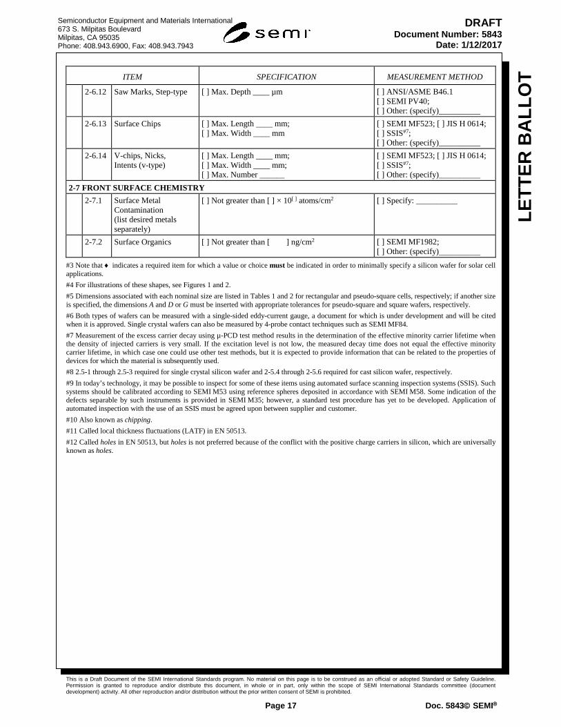
2-6.12 Saw Marks, Step-type [ ] Max. Depth ____ µm [ ] ANSI/ASME B46.1 [ ] SEMI PV40; [ ] Other: (specify)__________
2-6.13 Surface Chips [ ] Max. Length ____ mm; [ ] Max. Width ____ mm
[ ] SEMI MF523; [ ] JIS H 0614; [ ] SSIS#7; [ ] Other: (specify)__________
2-6.14 V-chips, Nicks, Intents (v-type)
[ ] Max. Length ____ mm; [ ] Max. Width ____ mm; [ ] Max. Number ______
[ ] SEMI MF523; [ ] JIS H 0614; [ ] SSIS#7; [ ] Other: (specify)__________
2-7 FRONT SURFACE CHEMISTRY 2-7.1 Surface Metal
Contamination (list desired metals separately)
[ ] Not greater than [ ] × 10[ ] atoms/cm2 [ ] Specify: __________
2-7.2 Surface Organics [ ] Not greater than [ ] ng/cm2 [ ] SEMI MF1982; [ ] Other: (specify)__________
#3 Note that ♦ indicates a required item for which a value or choice must be indicated in order to minimally specify a silicon wafer for solar cell applications. #4 For illustrations of these shapes, see Figures 1 and 2. #5 Dimensions associated with each nominal size are listed in Tables 1 and 2 for rectangular and pseudo-square cells, respectively; if another size is specified, the dimensions A and D or G must be inserted with appropriate tolerances for pseudo-square and square wafers, respectively. #6 Both types of wafers can be measured with a single-sided eddy-current gauge, a document for which is under development and will be cited when it is approved. Single crystal wafers can also be measured by 4-probe contact techniques such as SEMI MF84. #7 Measurement of the excess carrier decay using µ-PCD test method results in the determination of the effective minority carrier lifetime when the density of injected carriers is very small. If the excitation level is not low, the measured decay time does not equal the effective minority carrier lifetime, in which case one could use other test methods, but it is expected to provide information that can be related to the properties of devices for which the material is subsequently used. #8 2.5-1 through 2.5-3 required for single crystal silicon wafer and 2-5.4 through 2-5.6 required for cast silicon wafer, respectively. #9 In today’s technology, it may be possible to inspect for some of these items using automated surface scanning inspection systems (SSIS). Such systems should be calibrated according to SEMI M53 using reference spheres deposited in accordance with SEMI M58. Some indication of the defects separable by such instruments is provided in SEMI M35; however, a standard test procedure has yet to be developed. Application of automated inspection with the use of an SSIS must be agreed upon between supplier and customer. #10 Also known as chipping. #11 Called local thickness fluctuations (LATF) in EN 50513. #12 Called holes in EN 50513, but holes is not preferred because of the conflict with the positive charge carriers in silicon, which are universally known as holes.

This is a Draft Document of the SEMI International Standards program. No material on this page is to be construed as an official or adopted Standard or Safety Guideline. Permission is granted to reproduce and/or distribute this document, in whole or in part, only within the scope of SEMI International Standards committee (document development) activity. All other reproduction and/or distribution without the prior written consent of SEMI is prohibited.
Page 18 Doc. 5843 SEMI
Semiconductor Equipment and Materials International 673 S. Milpitas Boulevard Milpitas, CA 95035 Phone: 408.943.6900, Fax: 408.943.7943
LETT
ER B
ALL
OT
DRAFT Document Number: 5843
Date: 1/12/2017
RELATED INFORMATION 1 SOLAR CELL AREAS NOTICE: This Related Information is not an official part of SEMI PV22 and was derived from the work of the global Photovoltaic Technical Committee. This Related Information was approved for publication by full letter ballot procedures on September 12, 2011.
R1-1 Discussion R1-1.1 Calculations of the area of square and pseudo-square silicon wafers for solar cell use are listed for information only in TablesR1-1 and R1-2 of this section. These areas are the surface areas of the cell taking into account the areas lost to facets. Table R1-1 Cell Areas for Square Wafers
Cell Size Maximum Area, cm2 Target Area, cm2 Minimum Area, cm2
100 101.30 98.24 95.23 125 157.87 154.05 150.27 156 245.38 240.61 235.89 210 443.72 437.30 430.92
Cell Size Maximum Area, cm2 Target Area, cm2 Minimum Area, cm2
100.75 102.00 101.49 100.96 125.75 158.76 158.12 157.46 156.75 246.49 245.69 244.88 210.75 445.21 444.14 443.06
Table R1-2 Cell Areas for Pseudo-Square Wafers
Cell Size Maximum Area, cm2 Target Area, cm2 Minimum Area, cm2
100 98.26 97.17 95.95 125 149.57 148.57 147.45 156 243.14 240.85 238.46 210 444.32 440.55 436.57
Cell Size Maximum Area, cm2 Target Area, cm2 Minimum Area, cm2
100.75 99.12 98.65 98.18 125.75 150.99 150.42 149.86 156Ⅰ 243.59 242.84 242.09 156Ⅱ 245.07 244.31 243.55 210.75 444.69 443.65 442.61
NOTICE: SEMI makes no warranties or representations as to the suitability of the Standards and Safety Guidelines set forth herein for any particular application. The determination of the suitability of the Standard or Safety Guideline is solely the responsibility of the user. Users are cautioned to refer to manufacturer’s instructions, product labels, product data sheets, and other relevant literature, respecting any materials or equipment mentioned herein. Standards and Safety Guidelines are subject to change without notice.
By publication of this Standard or Safety Guideline, SEMI takes no position respecting the validity of any patent rights or copyrights asserted in connection with any items mentioned in this Standard or Safety Guideline. Users of this Standard or Safety Guideline are expressly advised that determination of any such patent rights or copyrights and the risk of infringement of such rights are entirely their own responsibility.