Back to Basics in Optical Communications Technologyjmfigueiredo/aulas/Optical... · • SONET/SDH...
178
Back to Basics in Optical Communications Technology
Transcript of Back to Basics in Optical Communications Technologyjmfigueiredo/aulas/Optical... · • SONET/SDH...
Back to Basics in Optical Communications
Technology
Back to Basics in Optical Communications TechnologyCopyright Agilent Technologies, 2002 2
Back to Basics in Optical Communications Technology
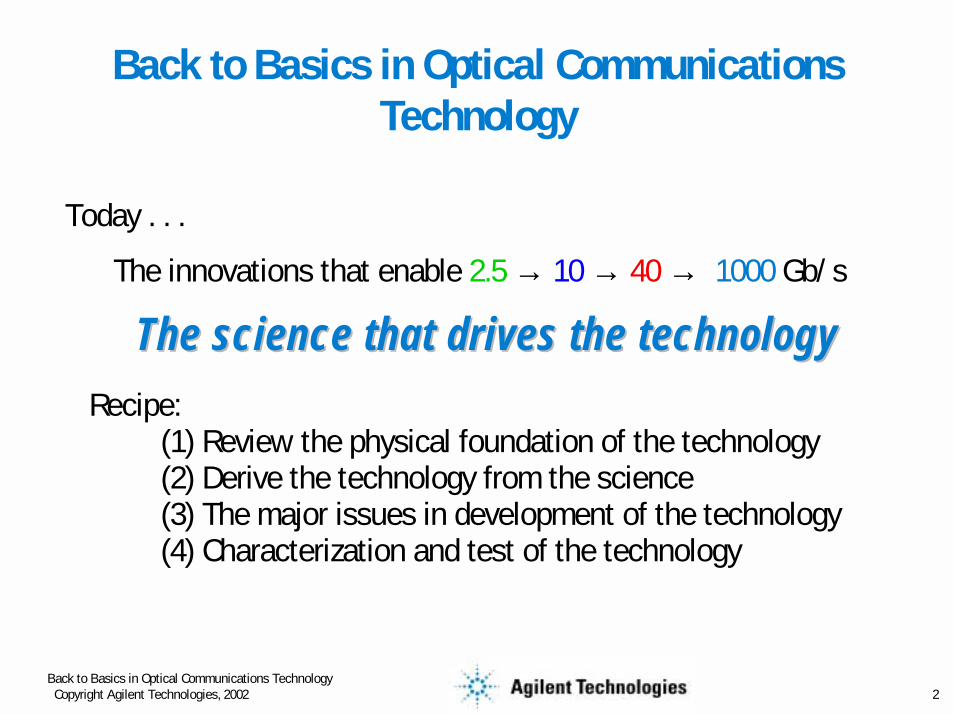
Today . . .The innovations that enable 2.5 → 10 → 40 → 1000 Gb/s
The science that drives the technologyThe science that drives the technologyRecipe:
(1) Review the physical foundation of the technology(2) Derive the technology from the science(3) The major issues in development of the technology(4) Characterization and test of the technology
Back to Basics in Optical Communications TechnologyCopyright Agilent Technologies, 2002 3
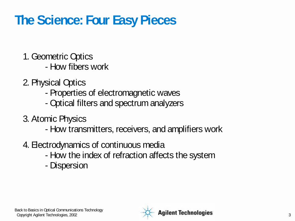
The Science: Four Easy Pieces
1. Geometric Optics - How fibers work
2. Physical Optics - Properties of electromagnetic waves- Optical filters and spectrum analyzers
3. Atomic Physics - How transmitters, receivers, and amplifiers work
4. Electrodynamics of continuous media - How the index of refraction affects the system- Dispersion
Back to Basics in Optical Communications TechnologyCopyright Agilent Technologies, 2002 4
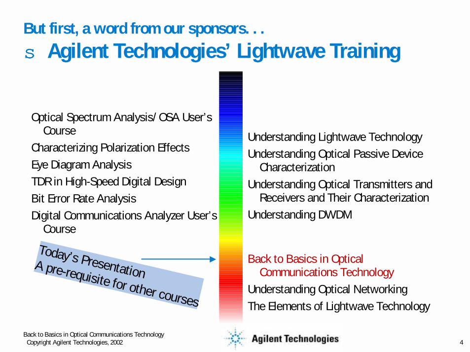
But first, a word from our sponsors. . .s s s s Agilent Technologies’ Lightwave Training
Understanding Lightwave TechnologyUnderstanding Optical Passive Device
CharacterizationUnderstanding Optical Transmitters and
Receivers and Their CharacterizationUnderstanding DWDM
Optical Spectrum Analysis/OSA User’s Course
Characterizing Polarization EffectsEye Diagram AnalysisTDR in High-Speed Digital DesignBit Error Rate AnalysisDigital Communications Analyzer User’s
Course
Back to Basics in Optical Communications Technology
Understanding Optical NetworkingThe Elements of Lightwave Technology
Today’s PresentationA pre-requisite for other courses
Back to Basics in Optical Communications TechnologyCopyright Agilent Technologies, 2002 5
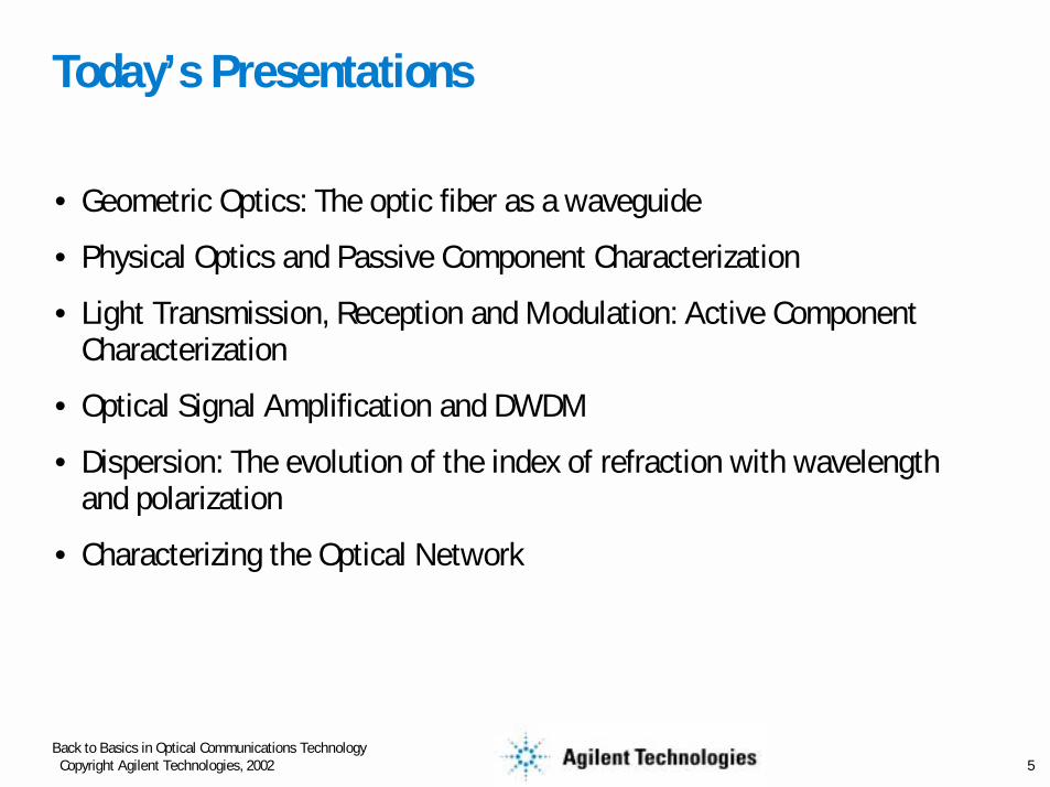
Today’s Presentations
• Geometric Optics: The optic fiber as a waveguide• Physical Optics and Passive Component Characterization• Light Transmission, Reception and Modulation: Active Component
Characterization• Optical Signal Amplification and DWDM• Dispersion: The evolution of the index of refraction with wavelength
and polarization• Characterizing the Optical Network

Back to Basics in Optical Communications TechnologyCopyright Agilent Technologies, 2002 6
High Speed NetworkingWhy we’re all here. . .
Back to Basics in Optical Communications TechnologyCopyright Agilent Technologies, 2002 7
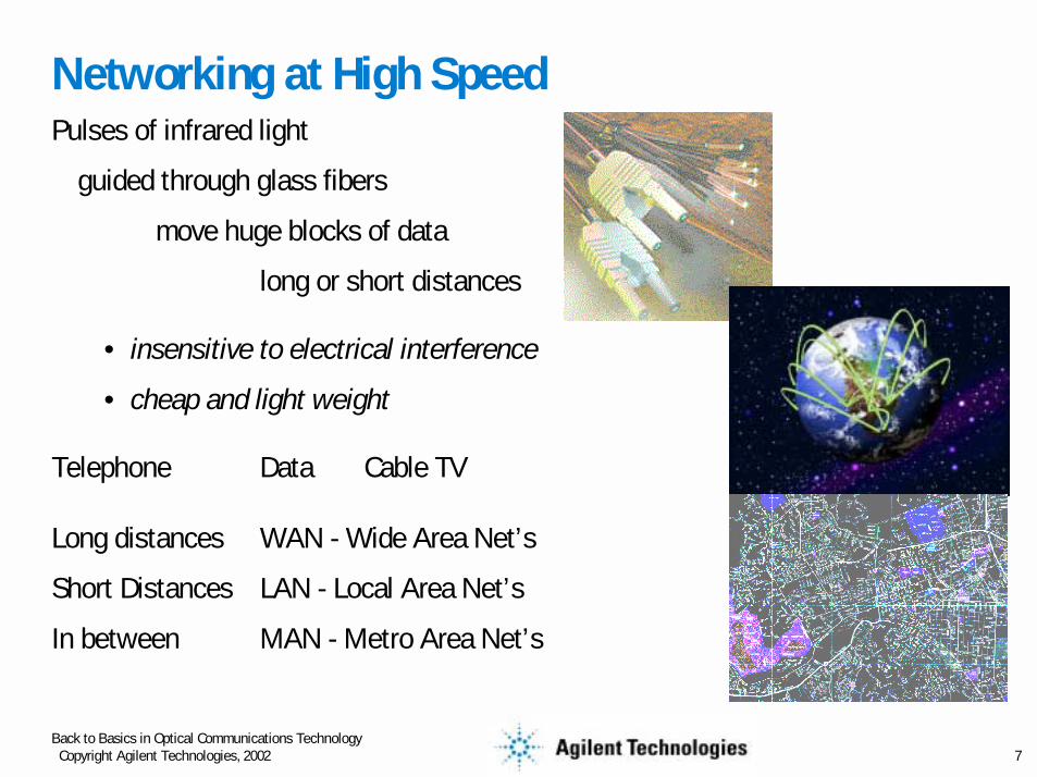
Networking at High SpeedPulses of infrared light
guided through glass fibersmove huge blocks of data
long or short distances
• insensitive to electrical interference• cheap and light weight
Telephone Data Cable TV
Long distances WAN - Wide Area Net’sShort Distances LAN - Local Area Net’sIn between MAN - Metro Area Net’s
Back to Basics in Optical Communications TechnologyCopyright Agilent Technologies, 2002 8
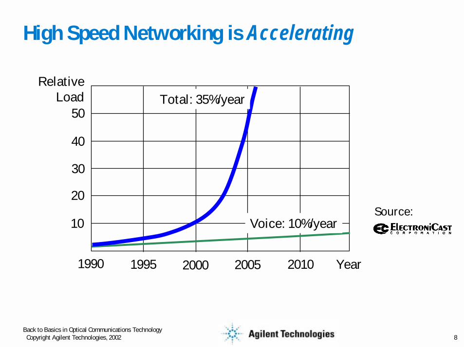
High Speed Networking is Accelerating
1995 2000 2005 2010 Year
10
20
30
40
50
RelativeLoad
1990
Total: 35%/year
Voice: 10%/yearSource:
Back to Basics in Optical Communications TechnologyCopyright Agilent Technologies, 2002 9
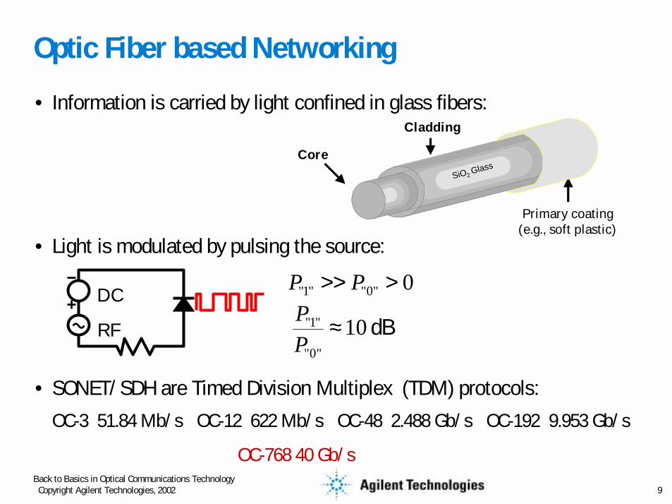
Optic Fiber based Networking• Information is carried by light confined in glass fibers:
• Light is modulated by pulsing the source:
• SONET/SDH are Timed Division Multiplex (TDM) protocols:OC-3 51.84 Mb/s OC-12 622 Mb/s OC-48 2.488 Gb/s OC-192 9.953 Gb/s
OC-768 40 Gb/s
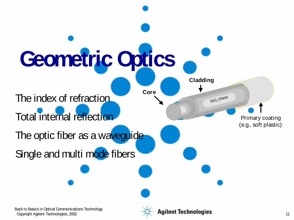
Cladding
Primary coating(e.g., soft plastic)
Core
SiO Glass2
DC
RF
0"0""1" >>> PP
dB 10"0"
"1" ≈PP
Back to Basics in Optical Communications TechnologyCopyright Agilent Technologies, 2002 10
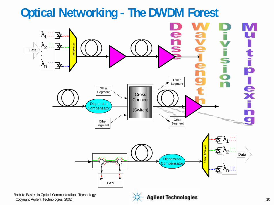
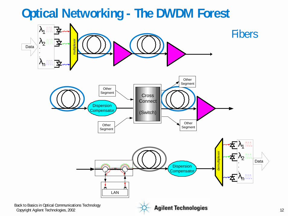
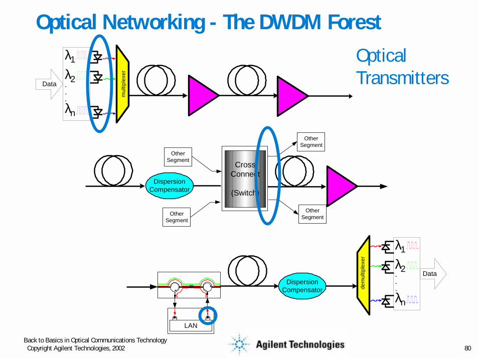
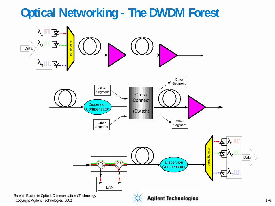
Optical Networking - The DWDM Forest
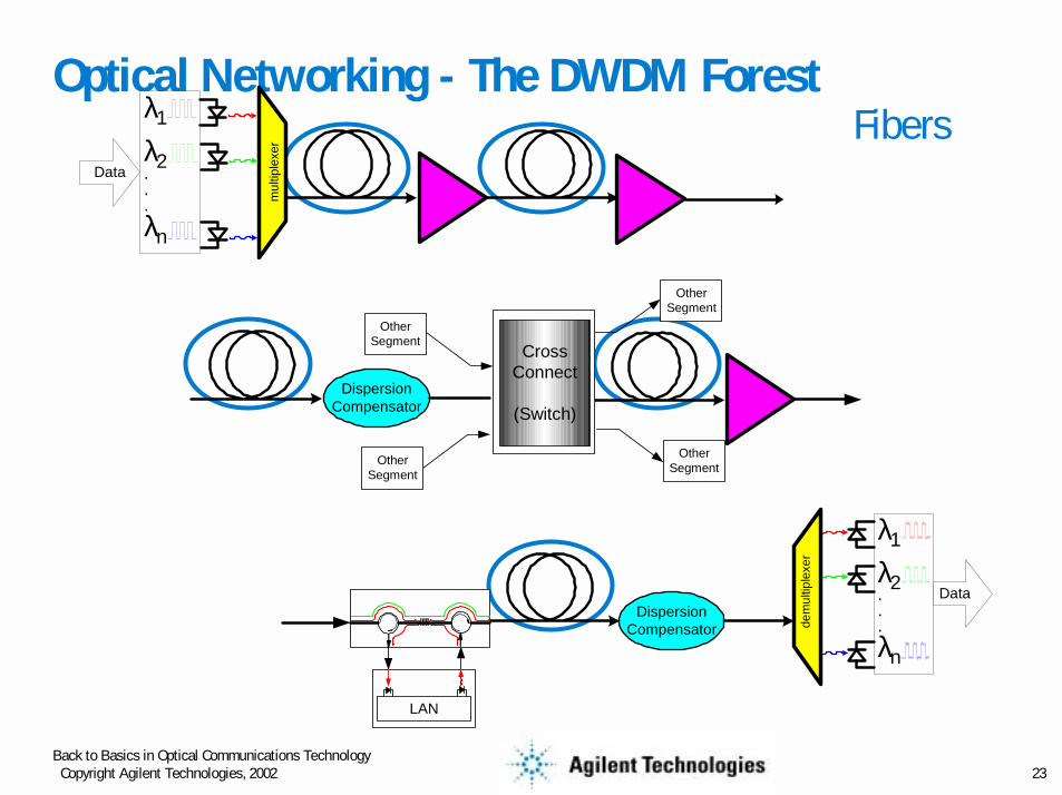
DispersionCompensator
DispersionCompensator
OtherSegment
OtherSegment
OtherSegment
OtherSegment
LAN
CrossConnect
(Switch)
Data
λ1
λ2...λn
Data
λ1
λ2...λn
dem
ultip
lexe
r
mul
tiple
xer
Back to Basics in Optical Communications TechnologyCopyright Agilent Technologies, 2002 11
Geometric OpticsThe index of refractionTotal internal reflectionThe optic fiber as a waveguideSingle and multi mode fibers
Cladding
Primary coating(e.g., soft plastic)
Core
SiO Glass2
Back to Basics in Optical Communications TechnologyCopyright Agilent Technologies, 2002 12
Optical Networking - The DWDM ForestFibers
DispersionCompensator
DispersionCompensator
OtherSegment
OtherSegment
OtherSegment
OtherSegment
LAN
CrossConnect
(Switch)
Data
λ1
λ2...λn
Data
λ1
λ2...λn
dem
ultip
lexe
r
mul
tiple
xer
Back to Basics in Optical Communications TechnologyCopyright Agilent Technologies, 2002 13
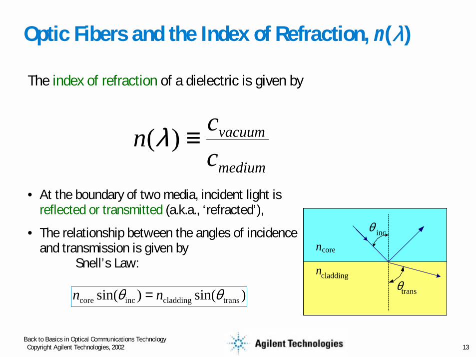
Optic Fibers and the Index of Refraction, n(λλλλ)
The index of refraction of a dielectric is given by
• At the boundary of two media, incident light is reflected or transmitted (a.k.a., ‘refracted’),
• The relationship between the angles of incidence and transmission is given by
Snell’s Law:
)sin()sin( transcladdinginccore θθ nn = transθcladdingn
ncore
incθ
medium
vacuum
ccn ≡)(λ
Back to Basics in Optical Communications TechnologyCopyright Agilent Technologies, 2002 14
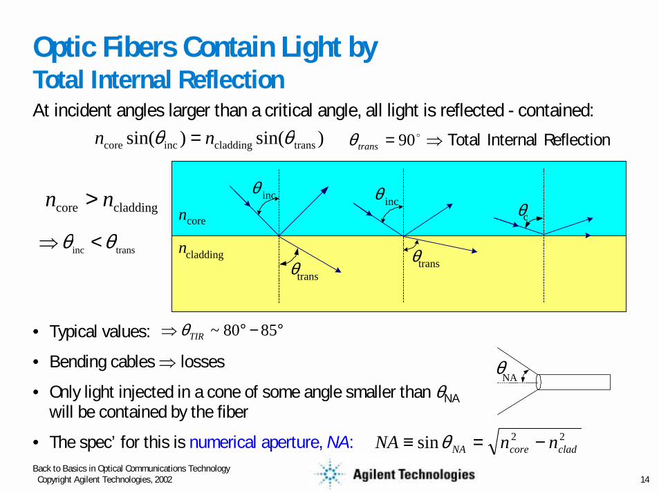
Optic Fibers Contain Light by Total Internal ReflectionAt incident angles larger than a critical angle, all light is reflected - contained:
• Typical values: • Bending cables ⇒ losses• Only light injected in a cone of some angle smaller than θNA
will be contained by the fiber• The spec’ for this is numerical aperture, NA:
claddingcore nn >
22sin cladcoreNA nnNA −=≡ θ
transinc θθ <⇒
θNA
transθcladdingn
ncore
incθincθ
transθ
cθ
°−°⇒ 8580~TIRθ
)sin()sin( transcladdinginccore θθ nn = Reflection Internal Total⇒= o90transθ
Back to Basics in Optical Communications TechnologyCopyright Agilent Technologies, 2002 15
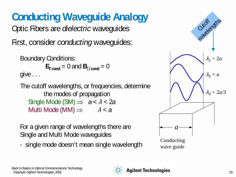
Conducting Waveguide AnalogyOptic Fibers are dielectric waveguidesFirst, consider conducting waveguides:
Conductingwave guide
Boundary Conditions:ET cond = 0 and B⊥⊥⊥⊥ cond = 0
give . . .
The cutoff wavelengths, or frequencies, determine the modes of propagation
Single Mode (SM) ⇒ a < λ < 2aMulti Mode (MM) ⇒ λ < a
For a given range of wavelengths there areSingle and Multi Mode waveguides- single mode doesn’t mean single wavelength
a
λ1 = 2a
λ2 = a
λ3 = 2a/3
Cutoff
wavelen
gths
Back to Basics in Optical Communications TechnologyCopyright Agilent Technologies, 2002 16
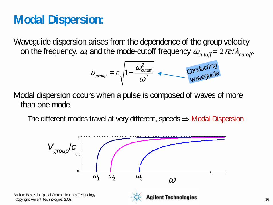
Modal Dispersion: Waveguide dispersion arises from the dependence of the group velocity
on the frequency, ω, and the mode-cutoff frequency ωcutoff = 2πc/λcutoff.
Modal dispersion occurs when a pulse is composed of waves of more than one mode.
The different modes travel at very different, speeds ⇒ Modal Dispersion
21ω
ωυ2cutoff−= cgroup
0
0.5
1
Vgroup/c
ωω1 ω2 ω3
Conducting
waveguide
Back to Basics in Optical Communications TechnologyCopyright Agilent Technologies, 2002 17
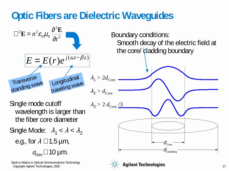
Optic Fibers are Dielectric WaveguidesBoundary conditions:
Smooth decay of the electric field at the core/cladding boundary
CladdingddCore
λ1 > 2dCore
λ2 > dCore
λ3 > 2 dCore /3
Single Mode: λ1 < λ < λ2
e.g., for λ ≅ 1.5 µm, dCore ≅ 10 µm.
Single mode cutoff wavelength is larger than the fiber core diameter
2
2
0022
tn
∂∂=∇ EE µε
)()( ztjerEE βω −=
Transverse
standing wave Longitudinal
traveling wave
Back to Basics in Optical Communications TechnologyCopyright Agilent Technologies, 2002 18
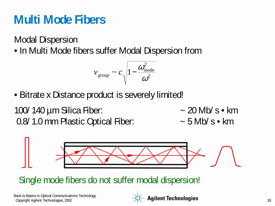
Multi Mode FibersModal Dispersion• In Multi Mode fibers suffer Modal Dispersion from
• Bitrate x Distance product is severely limited!100/140 µm Silica Fiber: ~ 20 Mb/s • km0.8/1.0 mm Plastic Optical Fiber: ~ 5 Mb/s • km
Single mode fibers do not suffer modal dispersion!
2
2mode1~
ωω−cvgroup
Back to Basics in Optical Communications TechnologyCopyright Agilent Technologies, 2002 19
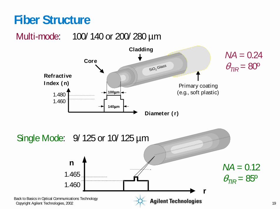
Fiber StructureMulti-mode: 100/140 or 200/280 µm
Single Mode: 9/125 or 10/125 µm
n
r
1.465
1.460
RefractiveIndex (n)
Diameter (r)
Cladding
Primary coating(e.g., soft plastic)
Core
1.4801.460
100µµµµm
140µµµµm
SiO Glass2
NA = 0.24θTIR = 80º
NA = 0.12θTIR = 85º
Back to Basics in Optical Communications TechnologyCopyright Agilent Technologies, 2002 20
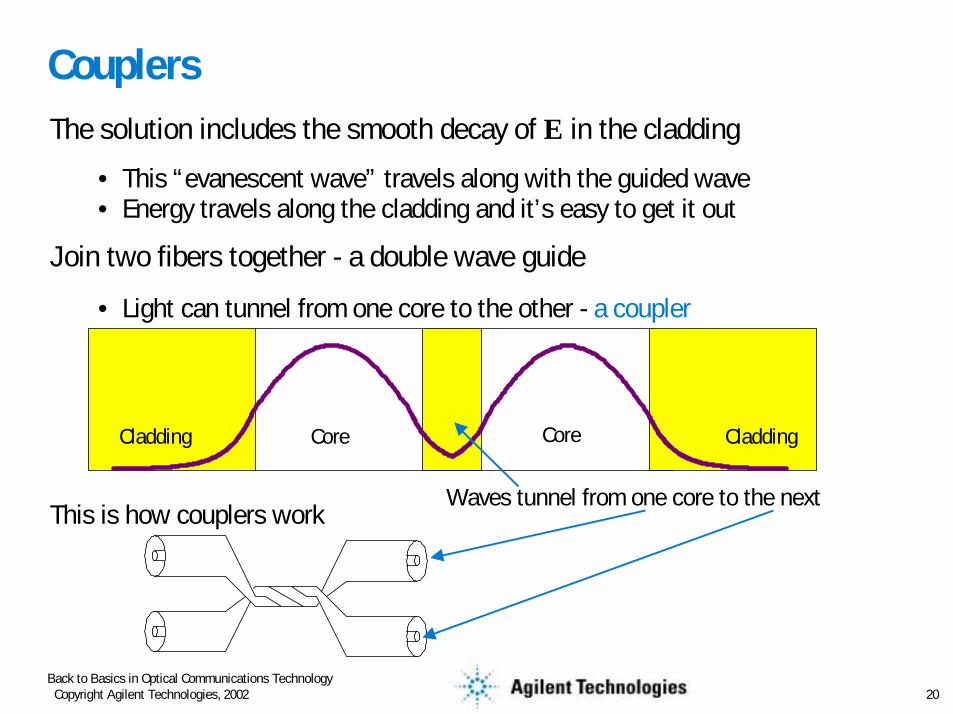
CouplersThe solution includes the smooth decay of E in the cladding
• This “evanescent wave” travels along with the guided wave• Energy travels along the cladding and it’s easy to get it out
Join two fibers together - a double wave guide• Light can tunnel from one core to the other - a coupler
This is how couplers work Waves tunnel from one core to the next
Core CoreCladding Cladding

Back to Basics in Optical Communications TechnologyCopyright Agilent Technologies, 2002 21
The Directional CouplerSingle Waveguide with Two Cores
Solving the wave equation with two single modecores gives . . .A transverse wave that oscillates between cores
End Side
d
• Incident signal power oscillates back and forth between the two cores as the light propagates the length of the coupler
The distance along the fiber where the signal is in a given core depends on . . .• Wavelength• The distance between the cores• The geometry of the two original single mode fibers
Back to Basics in Optical Communications TechnologyCopyright Agilent Technologies, 2002 22
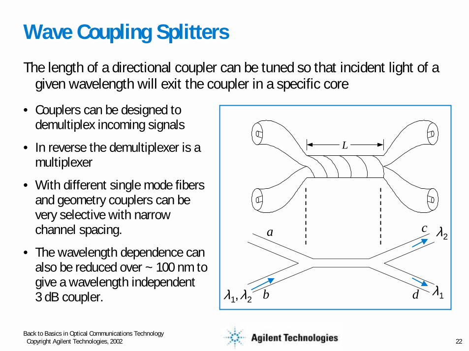
Wave Coupling SplittersThe length of a directional coupler can be tuned so that incident light of a
given wavelength will exit the coupler in a specific core
L
λ1, λ2
λ2
λ1
a
b
c
d
• Couplers can be designed to demultiplex incoming signals
• In reverse the demultiplexer is a multiplexer
• With different single mode fibers and geometry couplers can be very selective with narrow channel spacing.
• The wavelength dependence can also be reduced over ~ 100 nm to give a wavelength independent 3 dB coupler.
Back to Basics in Optical Communications TechnologyCopyright Agilent Technologies, 2002 23
Optical Networking - The DWDM ForestFibers
DispersionCompensator
DispersionCompensator
OtherSegment
OtherSegment
OtherSegment
OtherSegment
LAN
CrossConnect
(Switch)
Data
λ1
λ2...λn
Data
λ1
λ2...λn
dem
ultip
lexe
r
mul
tiple
xer
Back to Basics in Optical Communications TechnologyCopyright Agilent Technologies, 2002 24
Physical Opticsand
Passive Component Characterization
Back to Basics in Optical Communications TechnologyCopyright Agilent Technologies, 2002 25
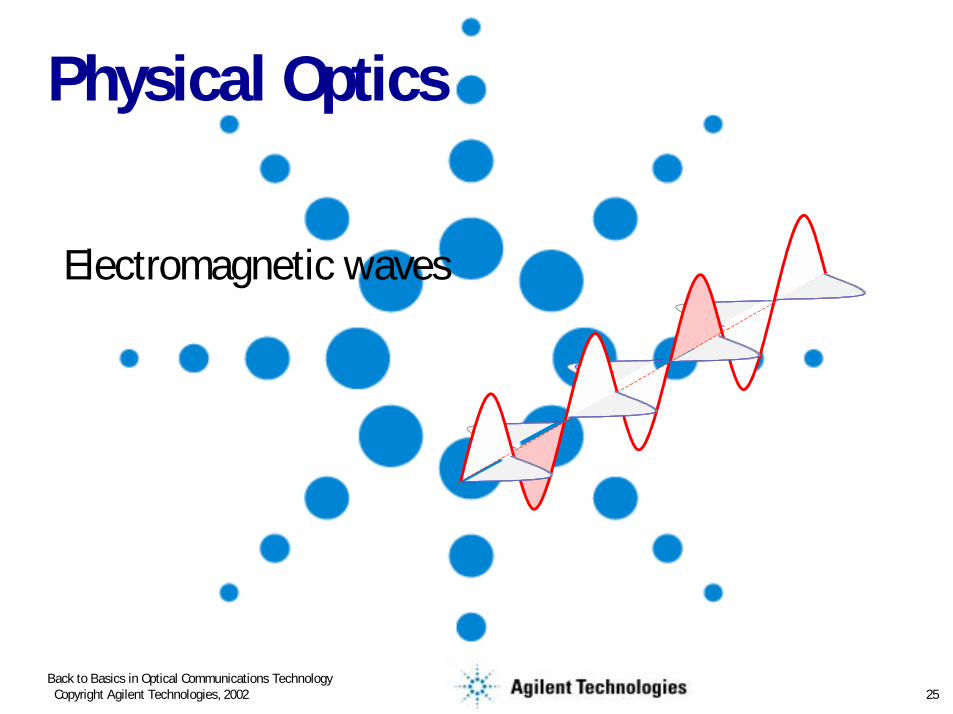
Physical Optics
Electromagnetic waves
Back to Basics in Optical Communications TechnologyCopyright Agilent Technologies, 2002 26
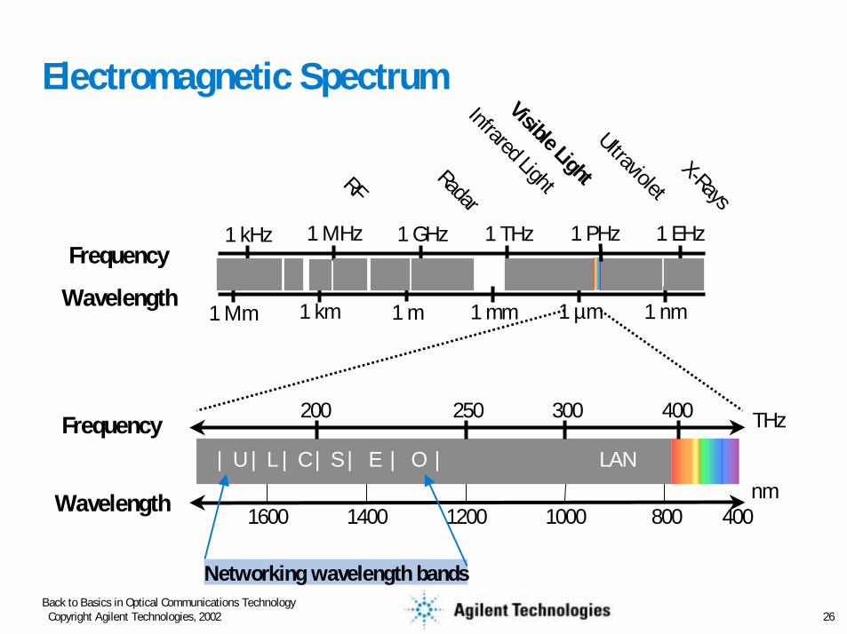
Electromagnetic Spectrum
Frequency
RF RadarInfrared Light
Visible LightUltraviolet
X-Rays
Wavelength 1 Mm 1 km 1 m 1 mm 1 nm1 µm
1 kHz 1 MHz 1 GHz 1 THz 1 EHz1 PHz
| U | L | C | S | E | O | LANFrequency
Wavelength 1600
300
1000 800nm
4001400 1200
THz200 250 400
Networking wavelength bands
Back to Basics in Optical Communications TechnologyCopyright Agilent Technologies, 2002 27
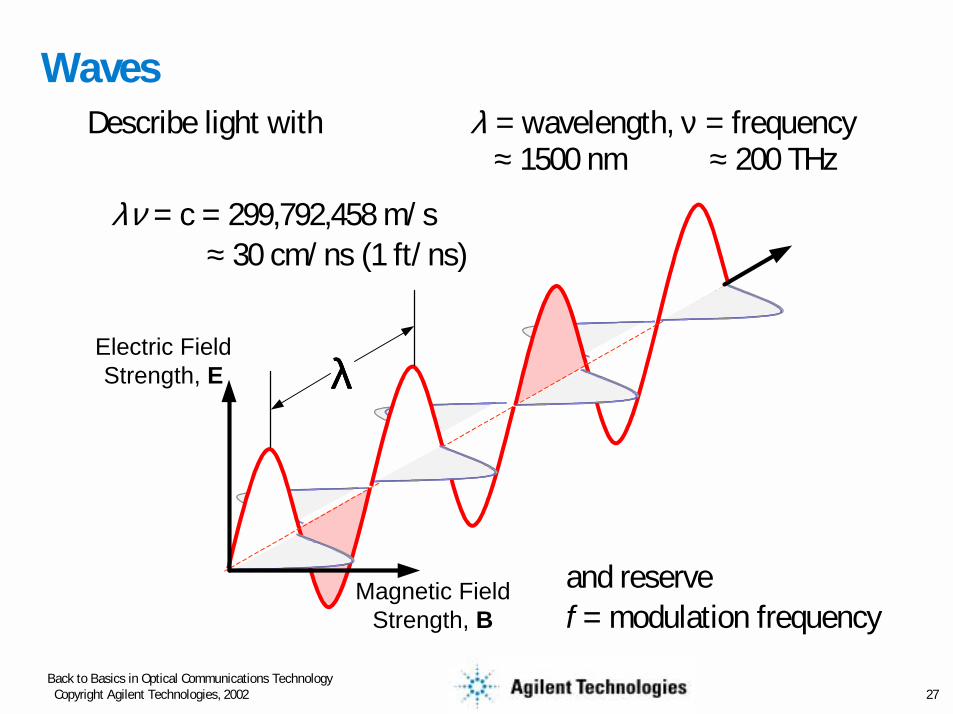
WavesDescribe light with λ = wavelength, ν = frequency
≈ 1500 nm ≈ 200 THzλν = c = 299,792,458 m/s
≈ 30 cm/ns (1 ft/ns)
and reservef = modulation frequency
λλλλ
Magnetic FieldStrength, B
Electric FieldStrength, E
Back to Basics in Optical Communications TechnologyCopyright Agilent Technologies, 2002 28
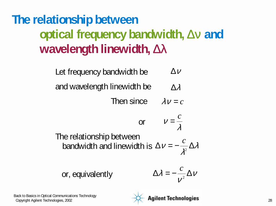
The relationship between optical frequency bandwidth, ∆ν∆ν∆ν∆ν and wavelength linewidth, ∆λ∆λ∆λ∆λ
Let frequency bandwidth be and wavelength linewidth be
Then since
orThe relationship between
bandwidth and linewidth is
or, equivalently
ν∆
λ∆
c=λν
λν c=
λλ
ν ∆−=∆2
c
νν
λ ∆−=∆2
c
Back to Basics in Optical Communications TechnologyCopyright Agilent Technologies, 2002 29
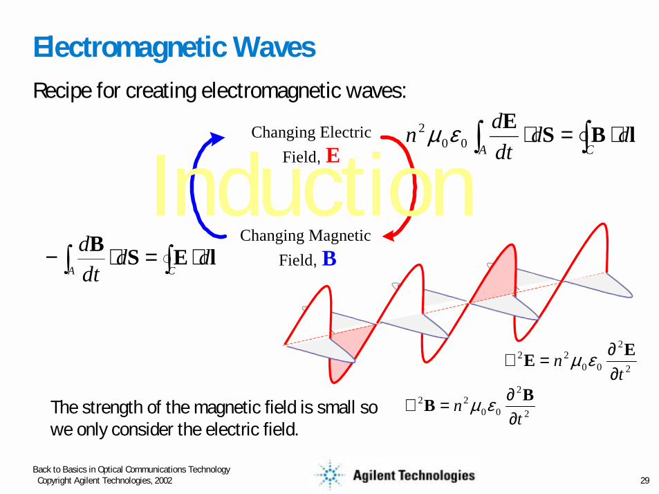
Recipe for creating electromagnetic waves:
∫∫ ⋅=⋅CA
dddtdn lBSE
002 εµ
∫∫ ⋅=⋅−CA
dddtd lESB
The strength of the magnetic field is small so we only consider the electric field.
Changing ElectricField, E
Changing Magnetic Field, B
2
2
0022
tn
∂∂=∇ EE εµ
2
2
0022
tn
∂∂=∇ BB εµ
Electromagnetic Waves
Induction
Back to Basics in Optical Communications TechnologyCopyright Agilent Technologies, 2002 30
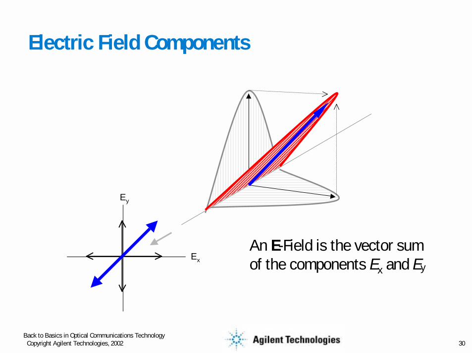
Electric Field Components
Ey
Ex
An E-Field is the vector sum of the components Ex and Ey
Back to Basics in Optical Communications TechnologyCopyright Agilent Technologies, 2002 31
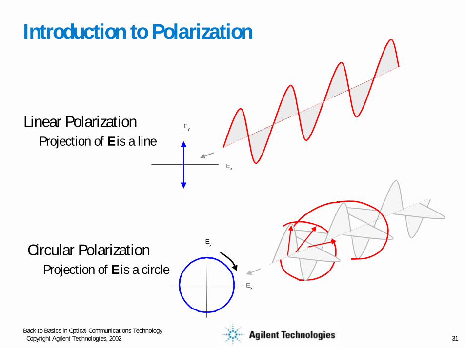
Introduction to Polarization
Linear PolarizationProjection of E is a line
Circular PolarizationProjection of E is a circle
Ey
Ex
Ey
Ex
Back to Basics in Optical Communications TechnologyCopyright Agilent Technologies, 2002 32
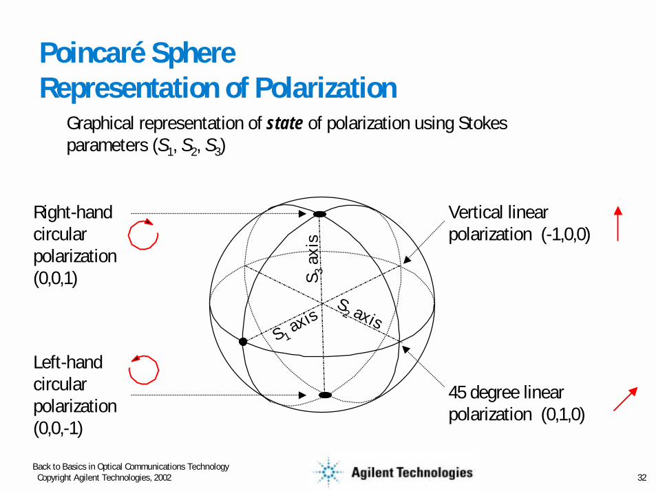
Poincaré Sphere Representation of Polarization
Graphical representation of state of polarization using Stokes parameters (S1, S2, S3)
Left-hand circular polarization (0,0,-1)
S 1axis
S2 axis
S 3ax
is
45 degree linearpolarization (0,1,0)
Right-hand circular polarization (0,0,1)
Vertical linearpolarization (-1,0,0)
Back to Basics in Optical Communications TechnologyCopyright Agilent Technologies, 2002 33
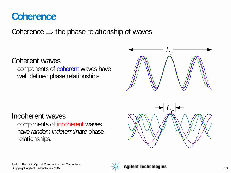
CoherenceCoherence ⇒ the phase relationship of waves
Lc
Lc
Coherent wavescomponents of coherent waves have well defined phase relationships.
Incoherent wavescomponents of incoherent waves have random indeterminate phase relationships.
Back to Basics in Optical Communications TechnologyCopyright Agilent Technologies, 2002 34
Coherence Time and Coherence LengthCoherence time (TC)
Average time for the wave train to lose its phase relationships
Coherence length (LC)Average distance over which superposed waves lose their phase relationships
There is a Fundamental Relationship between Coherence and Bandwidth
1. The bandwidth determines the coherence length and time, Tc ≈ 1/(4π ∆ν), Lc ≈ c/(4π ∆ν)
2. A minimum optical bandwidth is required for a pulse of duration ∆T, ∆ν ≈ 1/(4π∆T)
Restricts the spacing of DWDM signals for given rates
CC TcL ×=
πν 41≈×∆ CT
Short coherence length ⇔⇔⇔⇔ broadband source
Back to Basics in Optical Communications TechnologyCopyright Agilent Technologies, 2002 35
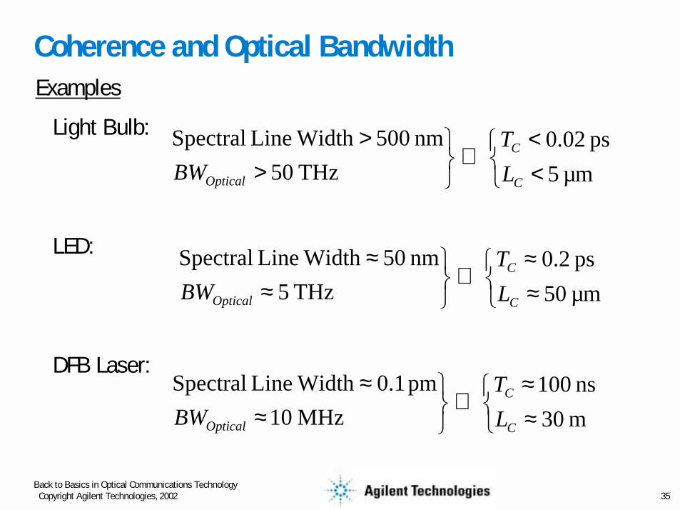
Coherence and Optical BandwidthExamples
Light Bulb:
LED:
DFB Laser:
<<
⇔
>>
µm5ps 02.0
THz50nm 500 Width Line Spectral
C
C
Optical LT
BW
≈≈
⇔
≈≈
µm50ps 2.0
THz5nm 50 Width Line Spectral
C
C
Optical LT
BW
≈≈
⇔
≈≈
m30ns 100
MHz10pm 1.0 Width Line Spectral
C
C
Optical LT
BW
Back to Basics in Optical Communications TechnologyCopyright Agilent Technologies, 2002 36
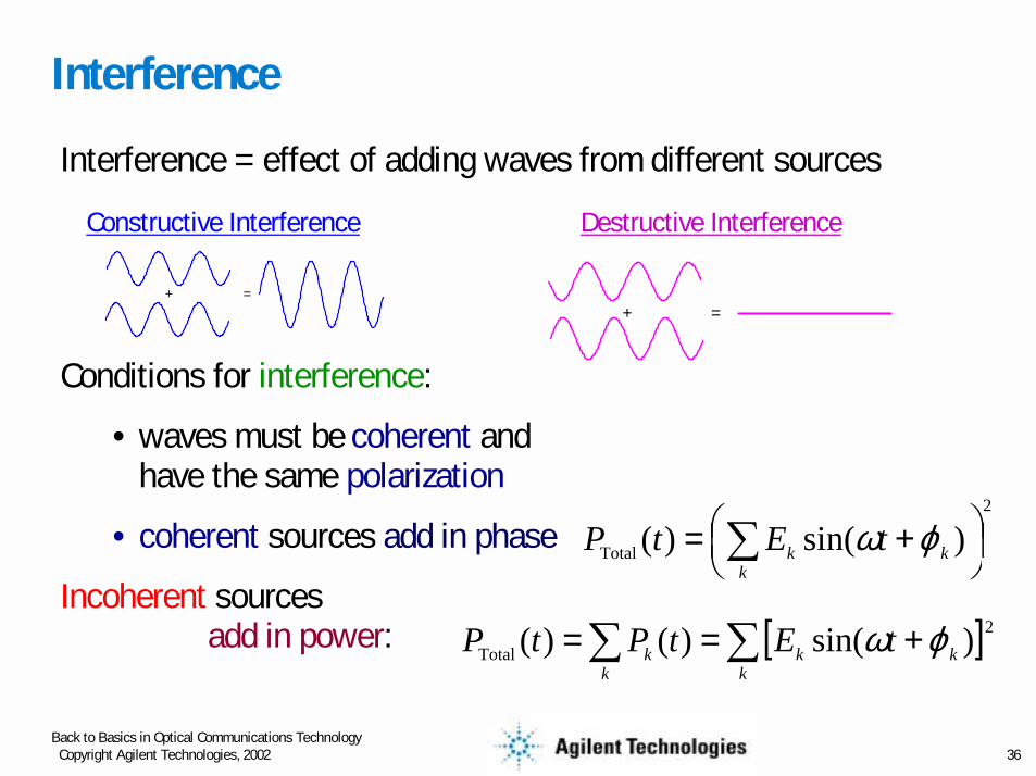
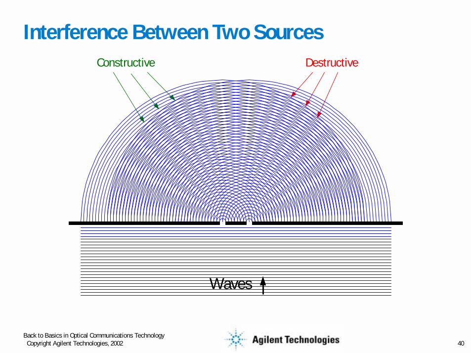
InterferenceInterference = effect of adding waves from different sources
Constructive Interference Destructive Interference
Conditions for interference:• waves must be coherent and
have the same polarization• coherent sources add in phase
Incoherent sources add in power: [ ]∑∑ +==
kkk
kk tEtPtP 2
Total )sin()()( ϕω
2
Total )sin()(
+= ∑
kkk tEtP ϕω
+ =+ =
Back to Basics in Optical Communications TechnologyCopyright Agilent Technologies, 2002 37
Physical Optics
Interference and Diffraction
Back to Basics in Optical Communications TechnologyCopyright Agilent Technologies, 2002 38
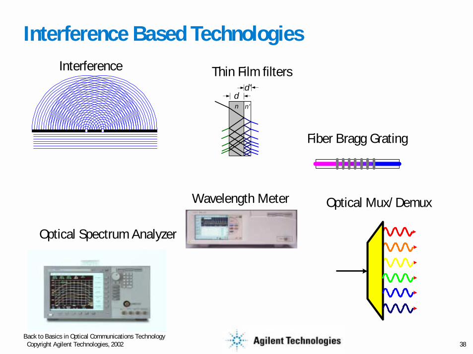
Interference Based TechnologiesInterference
Fiber Bragg Grating
Optical Mux/Demux
Optical Spectrum Analyzer
dd'
n n'
Thin Film filters
Wavelength Meter
Back to Basics in Optical Communications TechnologyCopyright Agilent Technologies, 2002 39
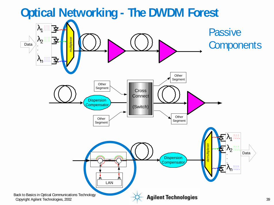
Optical Networking - The DWDM ForestPassive Components
DispersionCompensator
DispersionCompensator
OtherSegment
OtherSegment
OtherSegment
OtherSegment
LAN
CrossConnect
(Switch)
Data
λ1
λ2...λn
Data
λ1
λ2...λn
dem
ultip
lexe
r
mul
tiple
xer
Back to Basics in Optical Communications TechnologyCopyright Agilent Technologies, 2002 40
Interference Between Two SourcesConstructive Destructive
Waves
Back to Basics in Optical Communications TechnologyCopyright Agilent Technologies, 2002 41
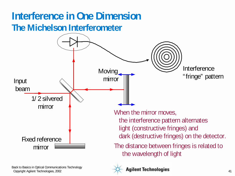
Interference in One Dimension The Michelson Interferometer
Input beam
Fixed reference mirror
Moving mirror
Interference “fringe” pattern
When the mirror moves, the interference pattern alternateslight (constructive fringes) and dark (destructive fringes) on the detector.
The distance between fringes is related to the wavelength of light
1/2 silveredmirror
Back to Basics in Optical Communications TechnologyCopyright Agilent Technologies, 2002 42
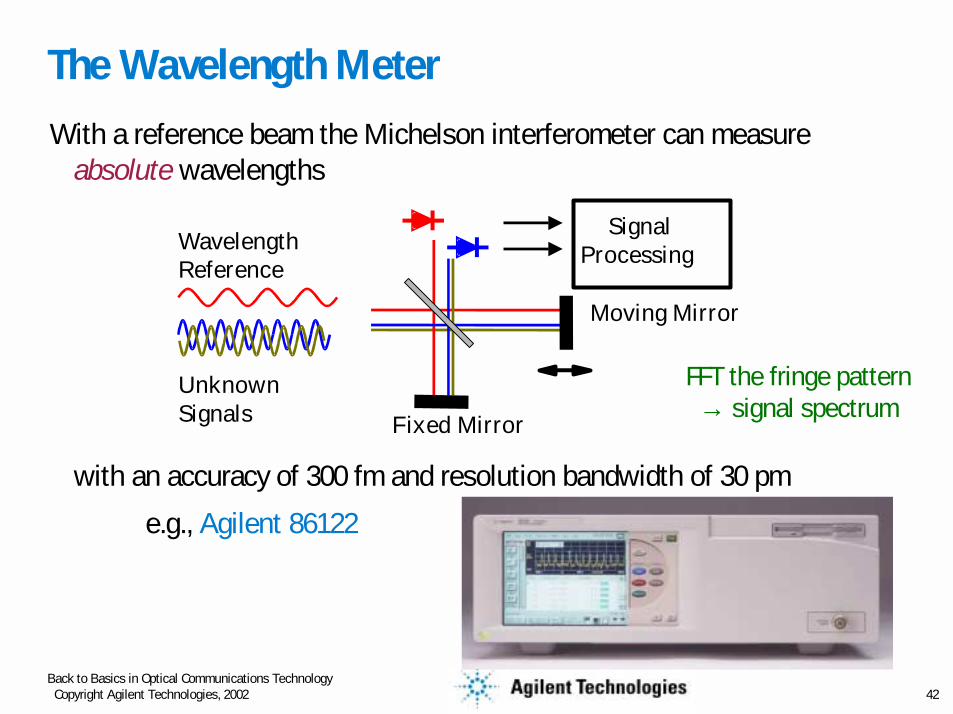
The Wavelength MeterWith a reference beam the Michelson interferometer can measure
absolute wavelengths
with an accuracy of 300 fm and resolution bandwidth of 30 pm e.g., Agilent 86122
WavelengthReference
UnknownSignals Fixed Mirror
SignalProcessing
Moving Mirror
FFT the fringe pattern → signal spectrum
Back to Basics in Optical Communications TechnologyCopyright Agilent Technologies, 2002 43
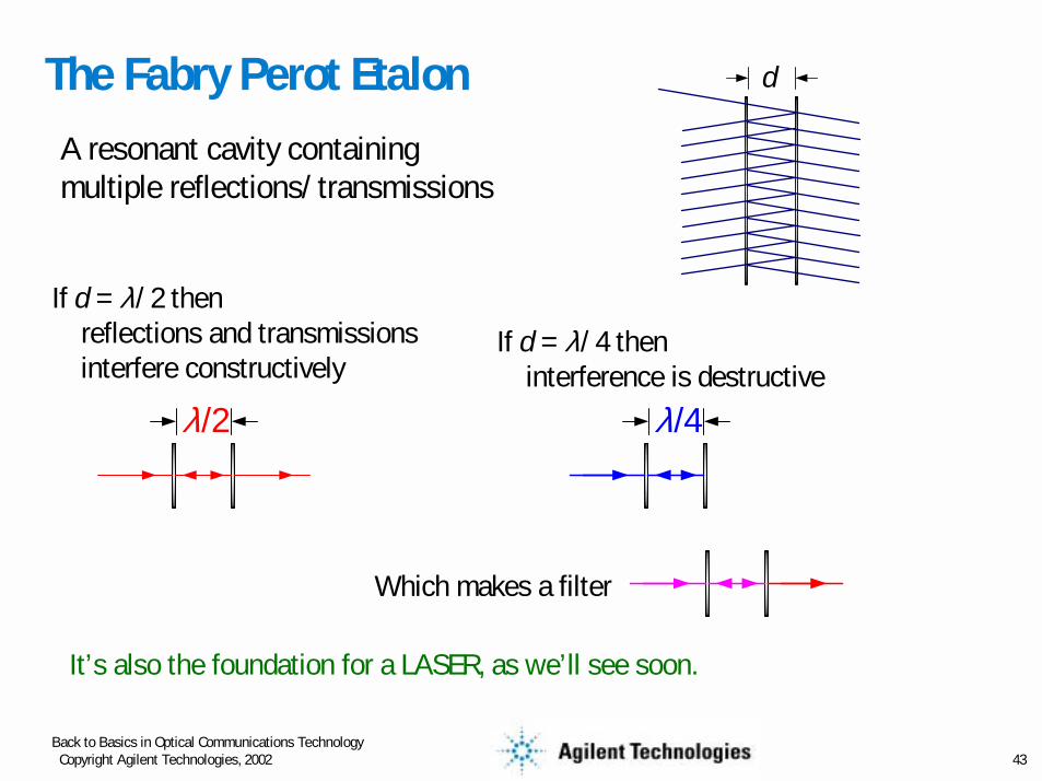
The Fabry Perot Etalon d
λ/2 λ/4
A resonant cavity containing multiple reflections/transmissions
If d = λ/2 thenreflections and transmissionsinterfere constructively
If d = λ/4 theninterference is destructive
Which makes a filter
It’s also the foundation for a LASER, as we’ll see soon.
Back to Basics in Optical Communications TechnologyCopyright Agilent Technologies, 2002 44
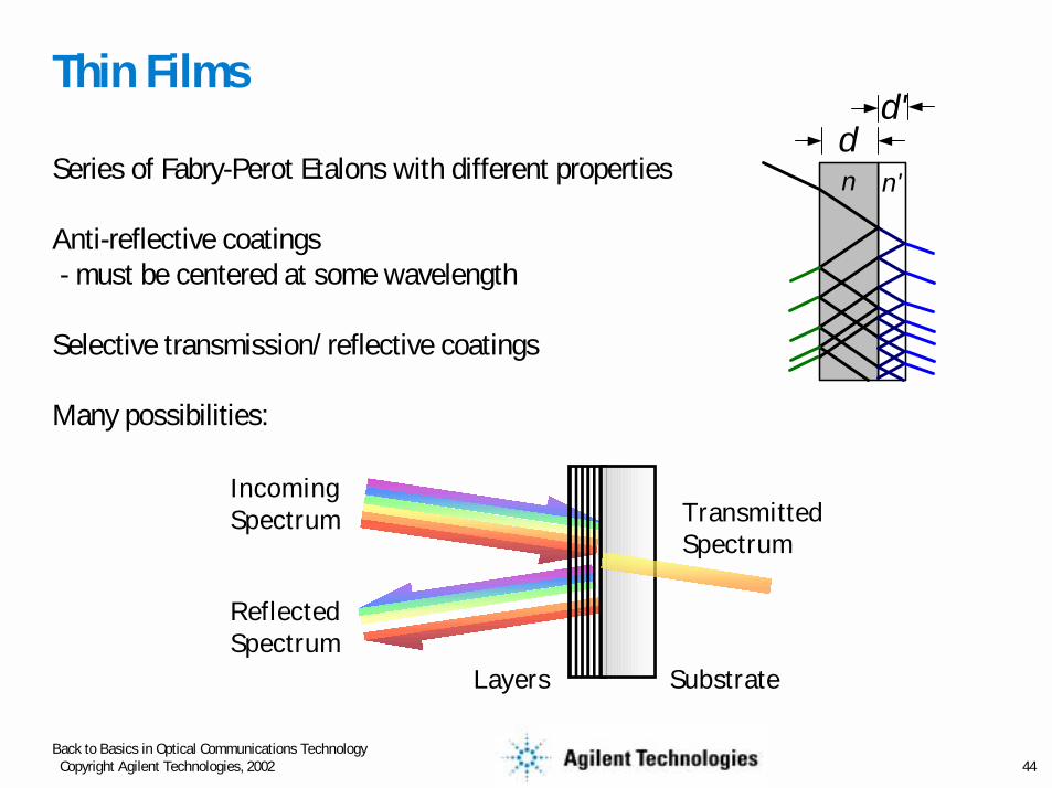
Thin Films
Series of Fabry-Perot Etalons with different properties
Anti-reflective coatings - must be centered at some wavelength
Selective transmission/reflective coatings
Many possibilities:
dd'
n n'
Layers Substrate
Incoming Spectrum
Reflected Spectrum
Transmitted Spectrum
Back to Basics in Optical Communications TechnologyCopyright Agilent Technologies, 2002 45
Tunable Fabry-Perot Filters
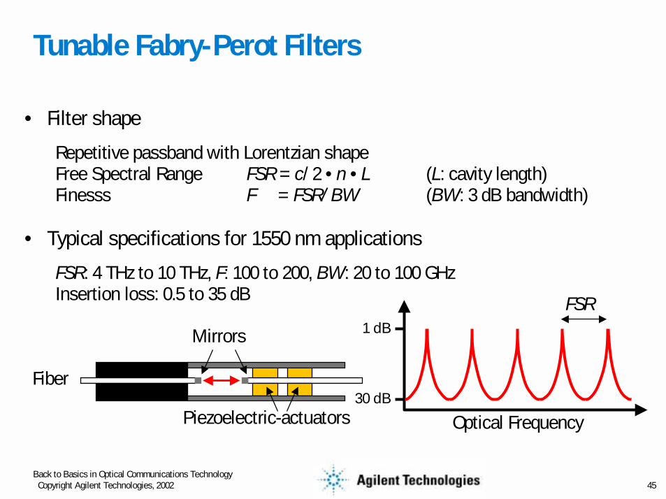
• Filter shapeRepetitive passband with Lorentzian shapeFree Spectral Range FSR = c/2 • n • L (L: cavity length)Finesss F = FSR/BW (BW: 3 dB bandwidth)
• Typical specifications for 1550 nm applicationsFSR: 4 THz to 10 THz, F: 100 to 200, BW: 20 to 100 GHzInsertion loss: 0.5 to 35 dB
Fiber
Piezoelectric-actuators
Mirrors
Optical Frequency
FSR1 dB
30 dB
Back to Basics in Optical Communications TechnologyCopyright Agilent Technologies, 2002 46
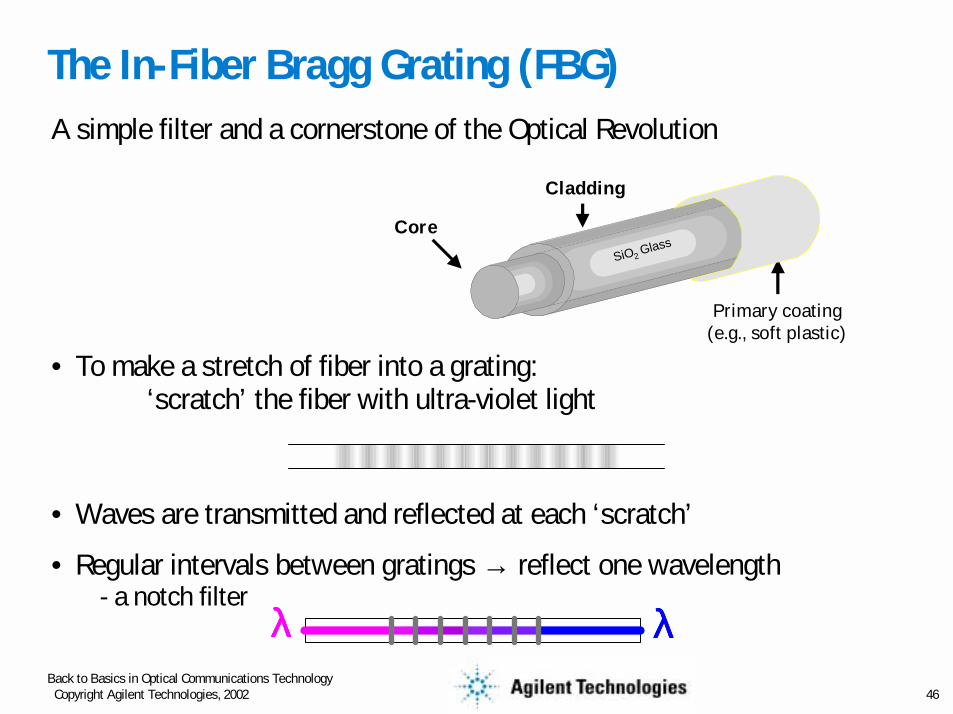
The In-Fiber Bragg Grating (FBG)A simple filter and a cornerstone of the Optical Revolution
• To make a stretch of fiber into a grating: ‘scratch’ the fiber with ultra-violet light
• Waves are transmitted and reflected at each ‘scratch’ • Regular intervals between gratings → reflect one wavelength
- a notch filter
Cladding
Primary coating(e.g., soft plastic)
Core
SiO Glass2
λλλλ λλλλ
Back to Basics in Optical Communications TechnologyCopyright Agilent Technologies, 2002 47
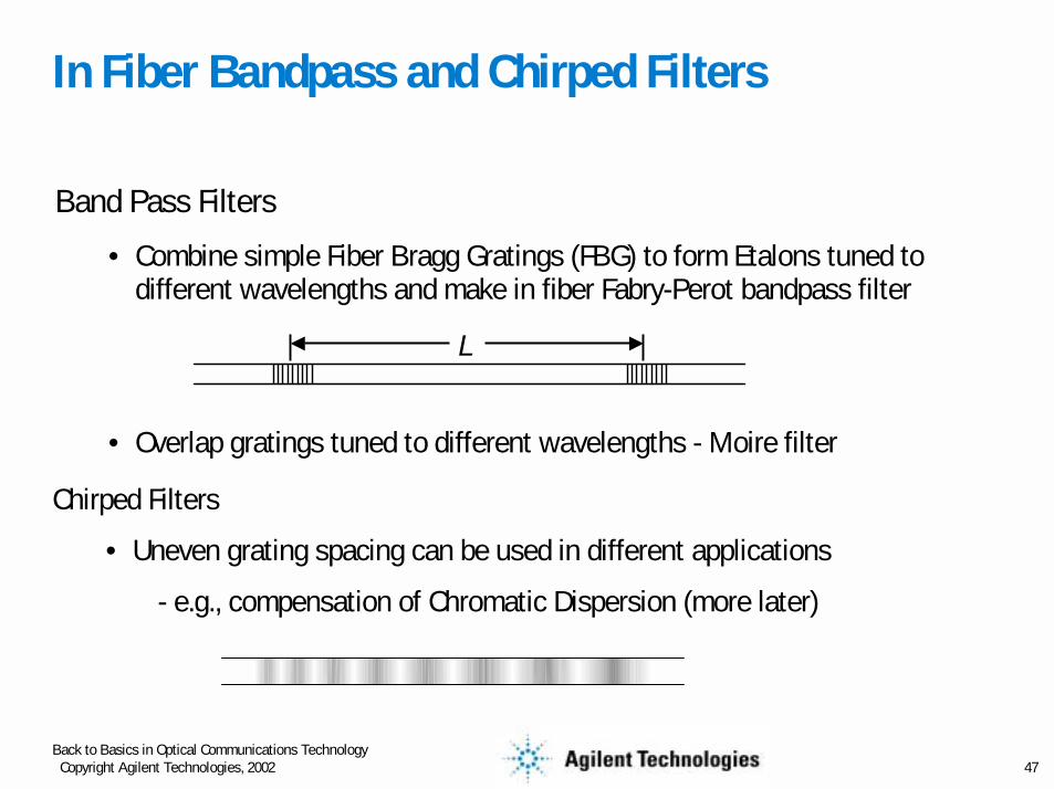
In Fiber Bandpass and Chirped Filters
Band Pass Filters• Combine simple Fiber Bragg Gratings (FBG) to form Etalons tuned to
different wavelengths and make in fiber Fabry-Perot bandpass filter
• Overlap gratings tuned to different wavelengths - Moire filter
L
Chirped Filters• Uneven grating spacing can be used in different applications
- e.g., compensation of Chromatic Dispersion (more later)
Back to Basics in Optical Communications TechnologyCopyright Agilent Technologies, 2002 48
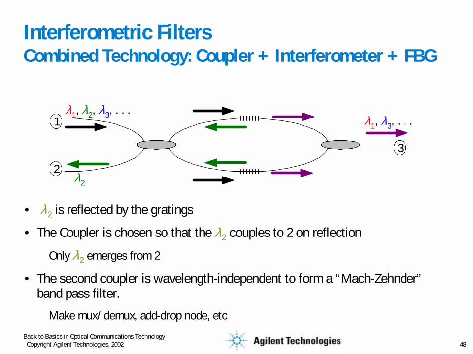
Interferometric FiltersCombined Technology: Coupler + Interferometer + FBG
• λ2 is reflected by the gratings • The Coupler is chosen so that the λ2 couples to 2 on reflection
Only λ2 emerges from 2
• The second coupler is wavelength-independent to form a “Mach-Zehnder” band pass filter.
Make mux/demux, add-drop node, etc
1
23
λ2
λ1, λ3, . . .λ1, λ2, λ3, . . .
Back to Basics in Optical Communications TechnologyCopyright Agilent Technologies, 2002 49
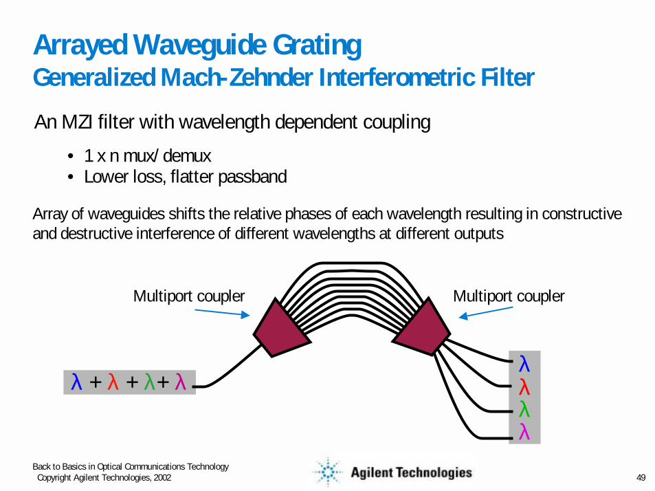
Arrayed Waveguide GratingGeneralized Mach-Zehnder Interferometric FilterAn MZI filter with wavelength dependent coupling
• 1 x n mux/demux• Lower loss, flatter passband
λ + λ + λ+ λλλλλ
Multiport coupler Multiport coupler
Array of waveguides shifts the relative phases of each wavelength resulting in constructive and destructive interference of different wavelengths at different outputs
Back to Basics in Optical Communications TechnologyCopyright Agilent Technologies, 2002 50
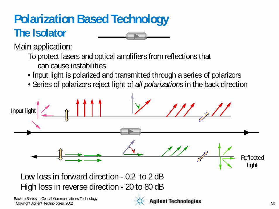
Low loss in forward direction - 0.2 to 2 dB High loss in reverse direction - 20 to 80 dB
Reflected light
Polarization Based TechnologyThe IsolatorMain application:
To protect lasers and optical amplifiers from reflections that can cause instabilities
• Input light is polarized and transmitted through a series of polarizors• Series of polarizors reject light of all polarizations in the back direction
Input light
Back to Basics in Optical Communications TechnologyCopyright Agilent Technologies, 2002 51
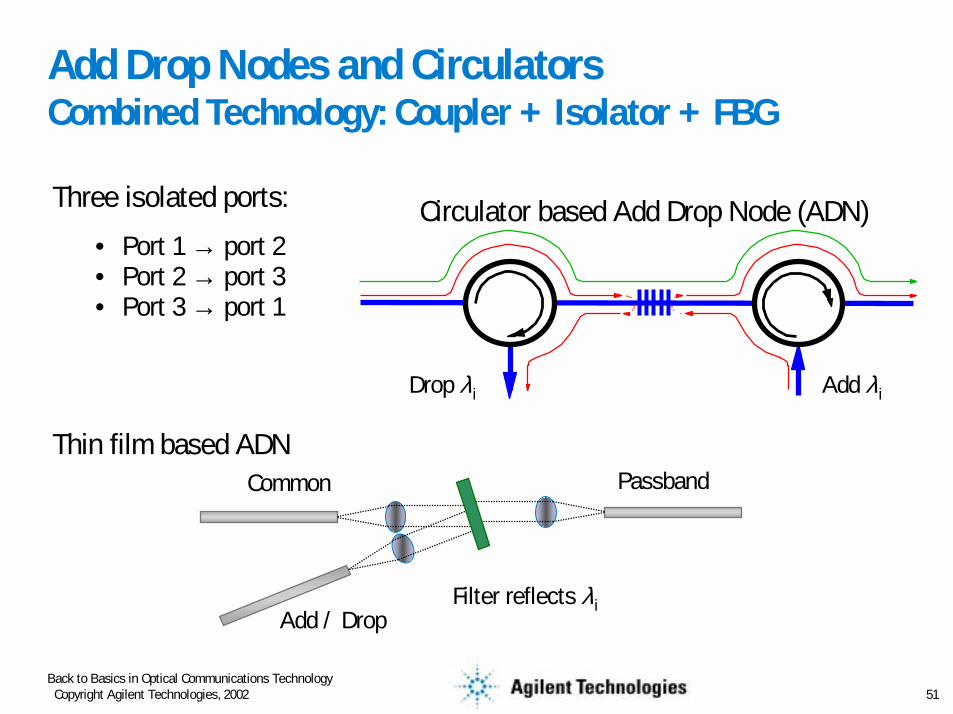
Add Drop Nodes and CirculatorsCombined Technology: Coupler + Isolator + FBG
Circulator based Add Drop Node (ADN)
Add λ iDrop λ i
Three isolated ports:• Port 1 → port 2• Port 2 → port 3• Port 3 → port 1
Filter reflects λ iAdd / Drop
Common PassbandThin film based ADN
Back to Basics in Optical Communications TechnologyCopyright Agilent Technologies, 2002 52
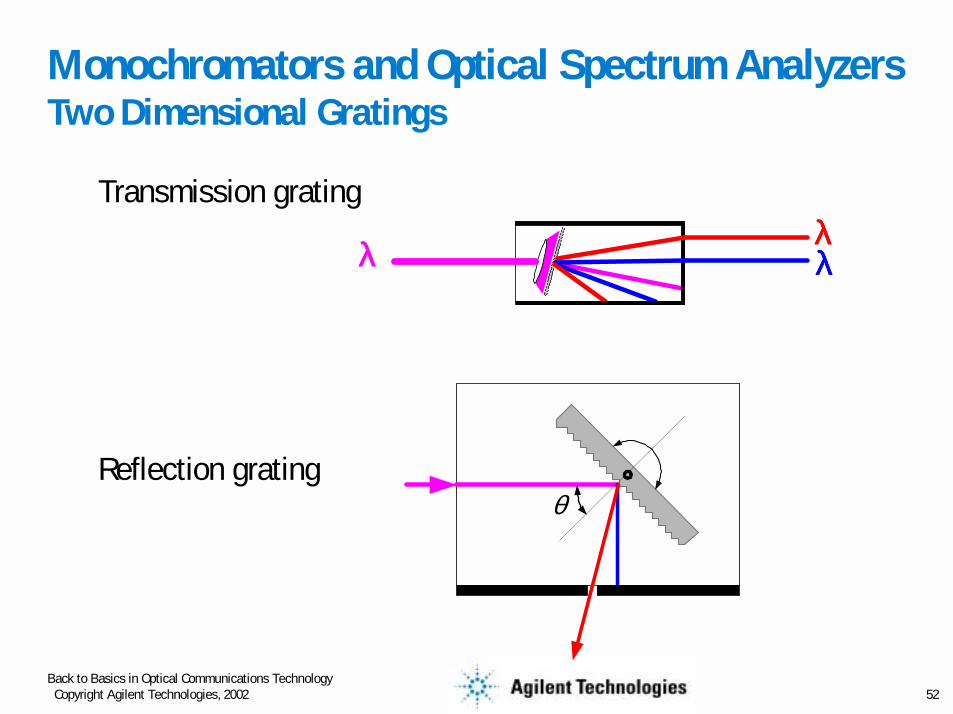
Monochromators and Optical Spectrum AnalyzersTwo Dimensional Gratings
Transmission grating
Reflection grating
λλλλλλλλλλλλ
θ
Back to Basics in Optical Communications TechnologyCopyright Agilent Technologies, 2002 53
Detector
Detector
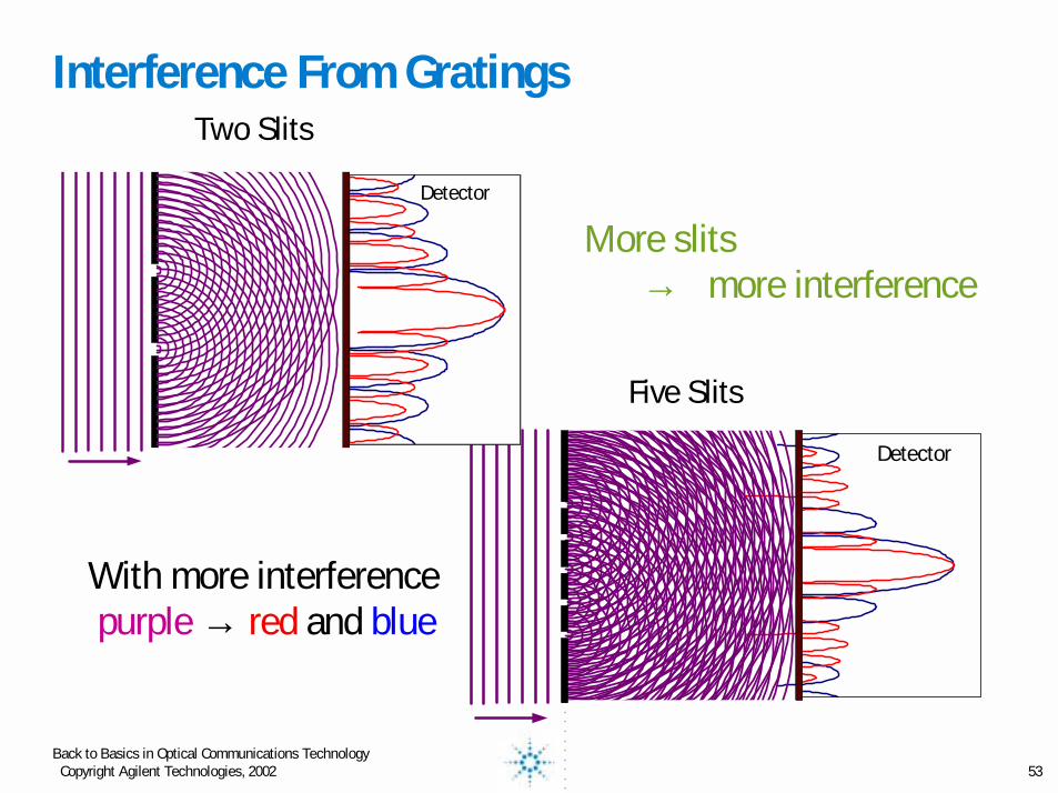
Interference From GratingsTwo Slits
Five Slits
More slits→ more interference
With more interferencepurple → red and blue
Back to Basics in Optical Communications TechnologyCopyright Agilent Technologies, 2002 54
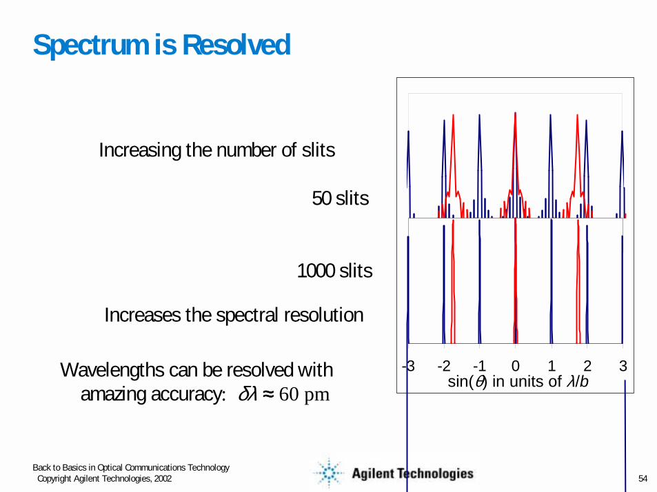
Spectrum is Resolved
-3 -2 -1 0 1 2 3
-3 -2 -1 0 1 2 3sin(θ) in units of λ/b
Increasing the number of slits
50 slits
1000 slits
Increases the spectral resolution
Wavelengths can be resolved with amazing accuracy: δλ ≈≈≈≈ 60 pm
Back to Basics in Optical Communications TechnologyCopyright Agilent Technologies, 2002 55
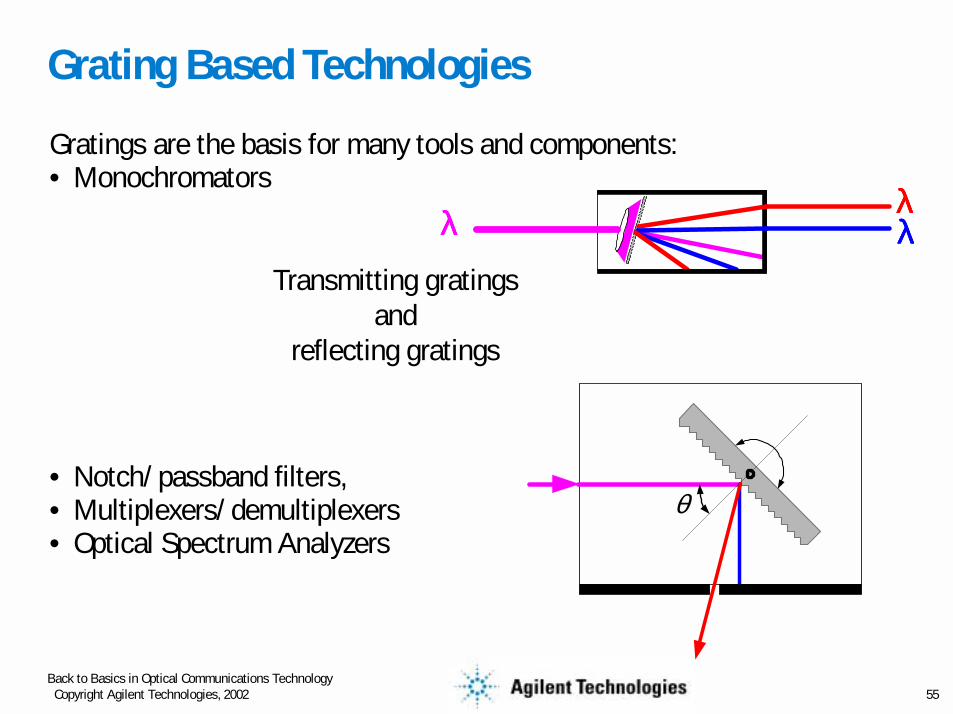
Grating Based TechnologiesGratings are the basis for many tools and components:• Monochromators
• Notch/passband filters,• Multiplexers/demultiplexers• Optical Spectrum Analyzers
λλλλλλλλλλλλ
θ
Transmitting gratingsand
reflecting gratings
Back to Basics in Optical Communications TechnologyCopyright Agilent Technologies, 2002 56
Grating Based Optical Spectrum Analyzer
θ
Rotate grating to shinedifferent color, λ,through aperture
Grating angle, θ, determines spectralline shining through aperture
ADC Processor
Amplifier
Display
Input
Photodiode
Aperture
Sweeping Monochromator
Back to Basics in Optical Communications TechnologyCopyright Agilent Technologies, 2002 57
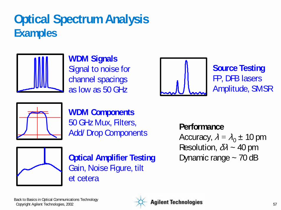
Optical Spectrum AnalysisExamples
Optical Amplifier TestingGain, Noise Figure, tiltet cetera
WDM Components50 GHz Mux, Filters, Add/Drop Components
WDM SignalsSignal to noise forchannel spacingsas low as 50 GHz
Source TestingFP, DFB lasersAmplitude, SMSR
PerformanceAccuracy, λ = λ0 ± 10 pmResolution, δλ ~ 40 pmDynamic range ~ 70 dB
Back to Basics in Optical Communications TechnologyCopyright Agilent Technologies, 2002 58
Physical Optics
Component Characterization
Back to Basics in Optical Communications TechnologyCopyright Agilent Technologies, 2002 59
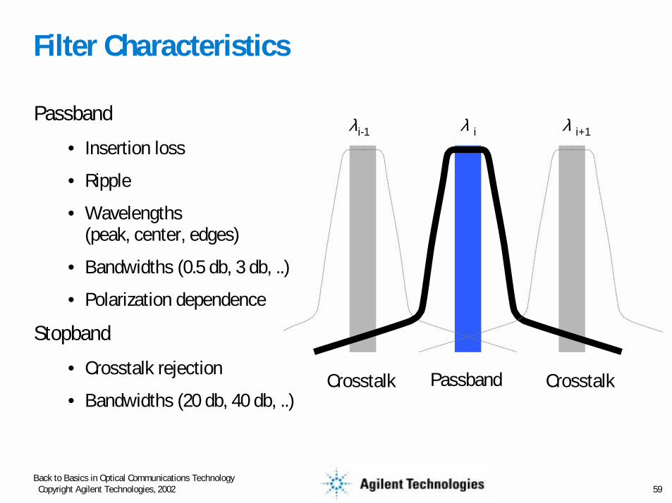
Filter Characteristics
λ i-1 λ i λ i+1
PassbandCrosstalk Crosstalk
Passband• Insertion loss• Ripple• Wavelengths
(peak, center, edges)• Bandwidths (0.5 db, 3 db, ..)• Polarization dependence
Stopband• Crosstalk rejection• Bandwidths (20 db, 40 db, ..)
Back to Basics in Optical Communications TechnologyCopyright Agilent Technologies, 2002 60
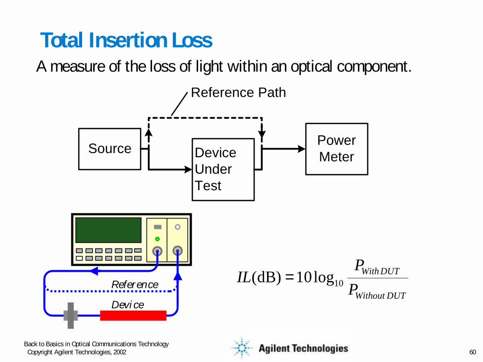
Total Insertion LossA measure of the loss of light within an optical component.
DUTWithout
DUTWith
PP
IL 10log10)dB( =Device
Reference
Source DeviceUnderTest
PowerMeter
Reference Path
Back to Basics in Optical Communications TechnologyCopyright Agilent Technologies, 2002 61
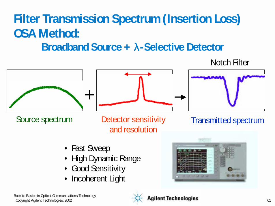
Filter Transmission Spectrum (Insertion Loss)OSA Method:
Broadband Source + λλλλ-Selective Detector
• Fast Sweep• High Dynamic Range• Good Sensitivity• Incoherent Light
Notch Filter
Source spectrum Detector sensitivityand resolution
Transmitted spectrum
Back to Basics in Optical Communications TechnologyCopyright Agilent Technologies, 2002 62
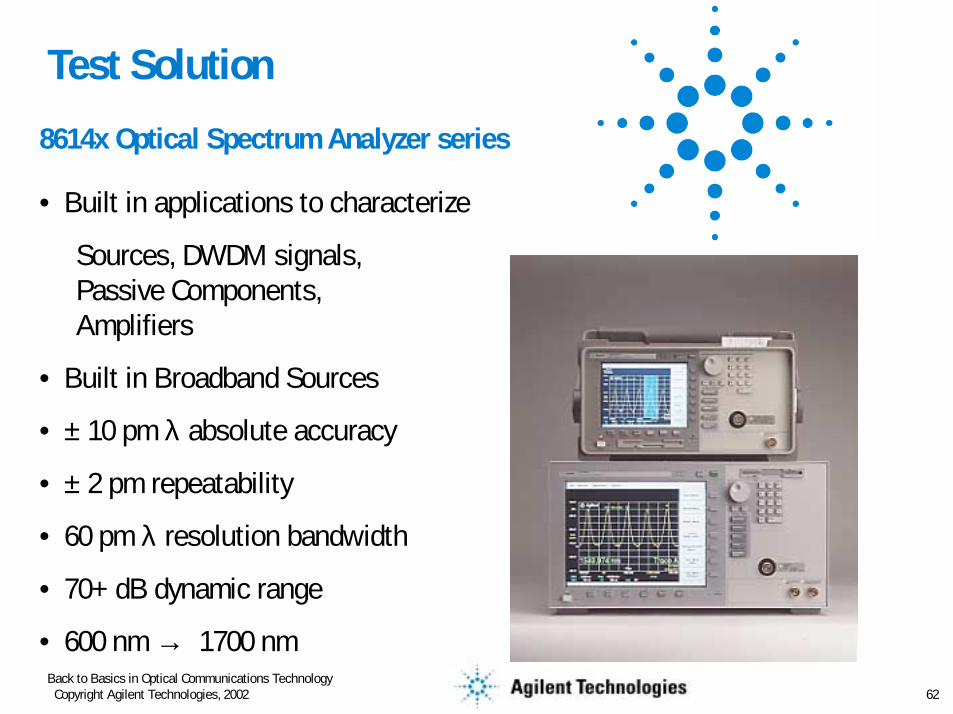
Test Solution8614x Optical Spectrum Analyzer series
• Built in applications to characterize
Sources, DWDM signals, Passive Components,Amplifiers
• Built in Broadband Sources
• ± 10 pm λ absolute accuracy
• ± 2 pm repeatability
• 60 pm λ resolution bandwidth
• 70+ dB dynamic range
• 600 nm → 1700 nm
Back to Basics in Optical Communications TechnologyCopyright Agilent Technologies, 2002 63
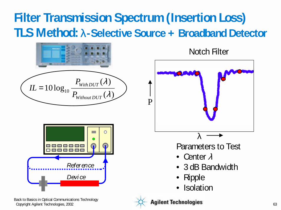
Filter Transmission Spectrum (Insertion Loss)TLS Method: λλλλ-Selective Source + Broadband Detector
Notch Filter
λ
P
Parameters to Test• Center λ• 3 dB Bandwidth• Ripple• Isolation
Device
Reference
)()(
log10 10 λλ
DUTWithout
DUTWith
PP
IL =
Back to Basics in Optical Communications TechnologyCopyright Agilent Technologies, 2002 64
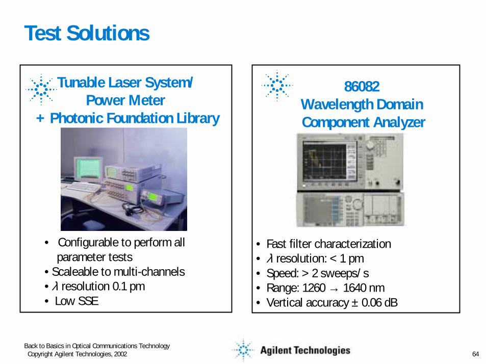
Test Solutions
86082 Wavelength Domain Component Analyzer
Tunable Laser System/Power Meter
+ Photonic Foundation Library
• Fast filter characterization• λ resolution: < 1 pm• Speed: > 2 sweeps/s• Range: 1260 → 1640 nm• Vertical accuracy ± 0.06 dB
• Configurable to perform all parameter tests
• Scaleable to multi-channels• λ resolution 0.1 pm• Low SSE
Back to Basics in Optical Communications TechnologyCopyright Agilent Technologies, 2002 65
Insertion Loss as a Function of WavelengthSwept Insertion Loss
Two standard approaches:
1.Use a Tunable Laser Source (TLS)• Worry about back scattering interference issues
2.Use a Broadband source and an OSA• Short coherence length of source ⇒ no interference issues• Must calibrate and subtract baseline spectrum• Need high spectral density (energy at each wavelength)
Reference p/n 5980-1454E:State of the art characterization of optical components for DWDM applications
Back to Basics in Optical Communications TechnologyCopyright Agilent Technologies, 2002 66
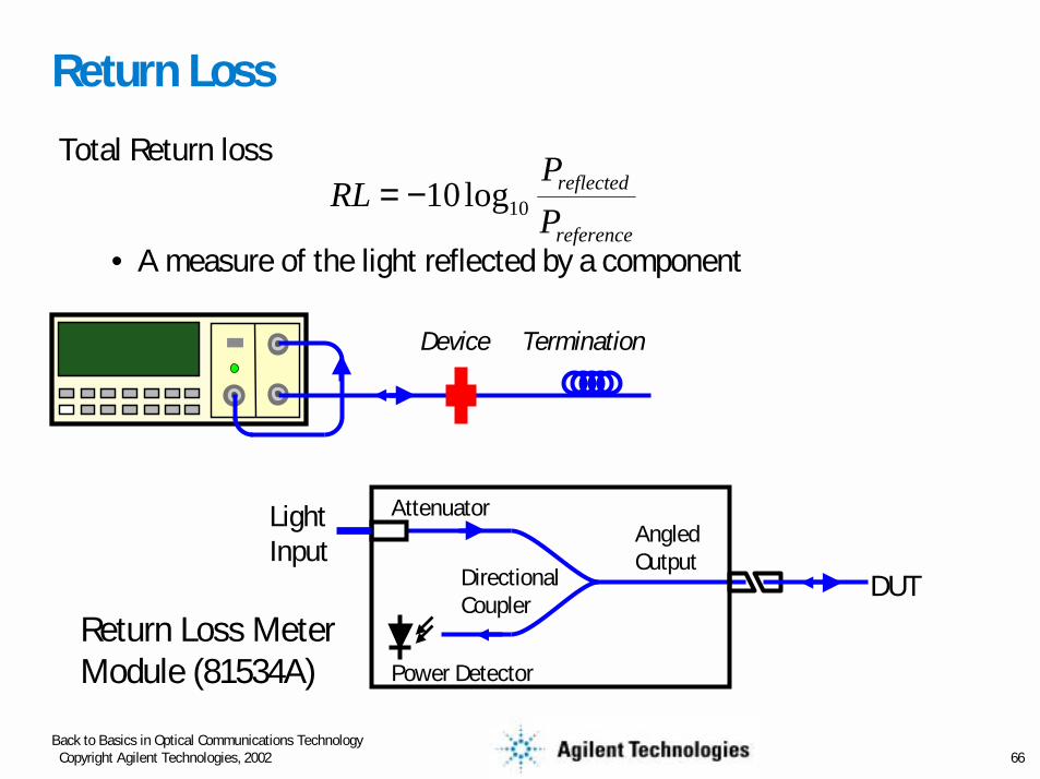
Return LossTotal Return loss
• A measure of the light reflected by a componentreference
reflected
PP
RL 10log10−=
Device Termination
Light Input
Attenuator
Power Detector
Angled OutputDirectional
CouplerDUT
Return Loss MeterModule (81534A)
Back to Basics in Optical Communications TechnologyCopyright Agilent Technologies, 2002 67
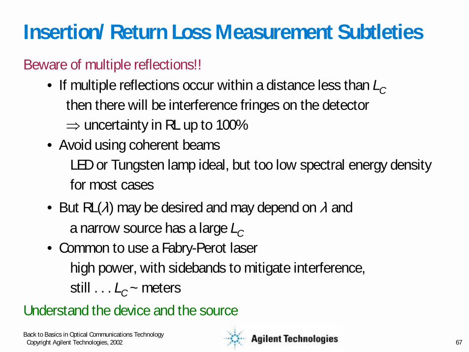
Insertion/Return Loss Measurement SubtletiesBeware of multiple reflections!!
• If multiple reflections occur within a distance less than LCthen there will be interference fringes on the detector⇒ uncertainty in RL up to 100%
• Avoid using coherent beamsLED or Tungsten lamp ideal, but too low spectral energy densityfor most cases
• But RL(λ) may be desired and may depend on λ anda narrow source has a large LC
• Common to use a Fabry-Perot laserhigh power, with sidebands to mitigate interference,still . . . LC ~ meters
Understand the device and the source
Back to Basics in Optical Communications TechnologyCopyright Agilent Technologies, 2002 68
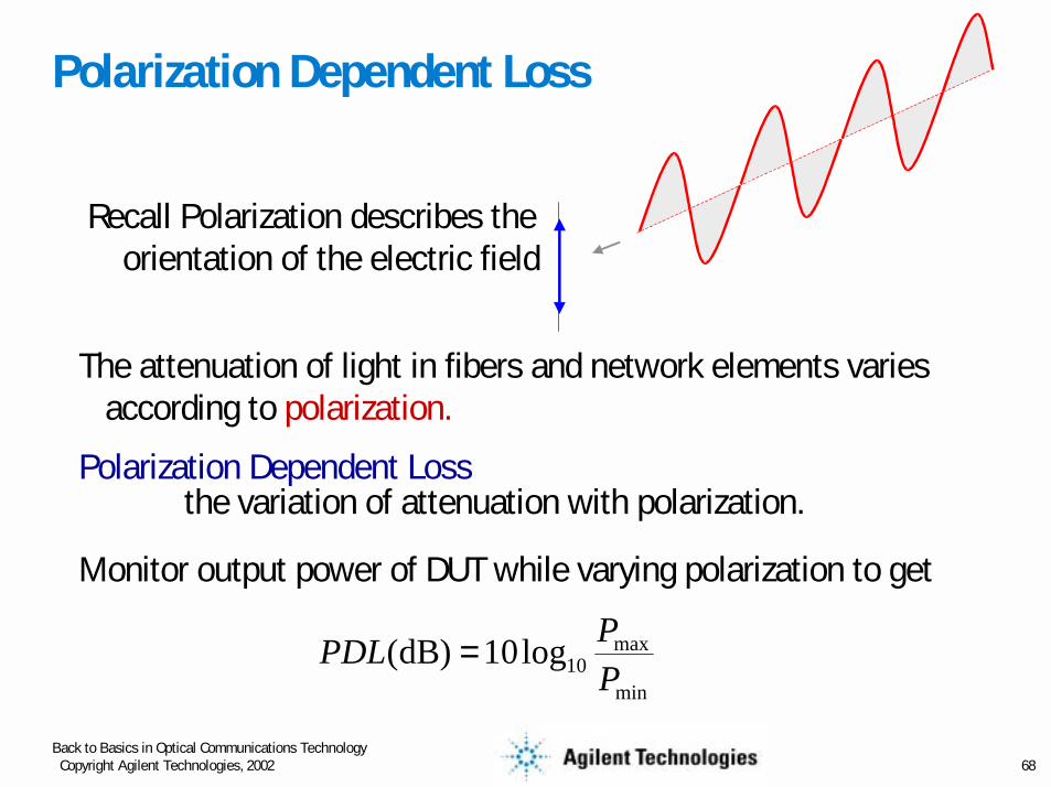
Polarization Dependent Loss
Recall Polarization describes the orientation of the electric field
The attenuation of light in fibers and network elements varies according to polarization.
Polarization Dependent Lossthe variation of attenuation with polarization.
Monitor output power of DUT while varying polarization to get
min
max10log10)dB(
PPPDL =
Back to Basics in Optical Communications TechnologyCopyright Agilent Technologies, 2002 69
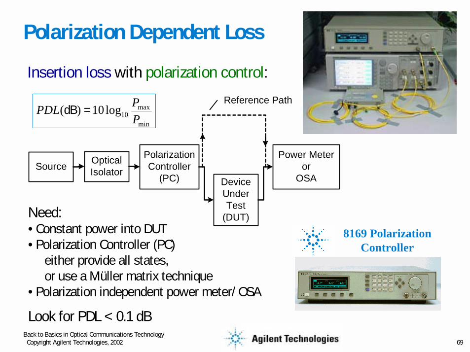
Polarization Dependent Loss
Insertion loss with polarization control:
SourceDeviceUnderTest
(DUT)
Power Meteror
OSA
OpticalIsolator
PolarizationController
(PC)
Reference Path
Need:• Constant power into DUT• Polarization Controller (PC)
either provide all states, or use a Müller matrix technique
• Polarization independent power meter/OSA
Look for PDL < 0.1 dB
8169 Polarization Controller
min
max10log10)(
PPPDL =dB

Back to Basics in Optical Communications TechnologyCopyright Agilent Technologies, 2002 70
Optical Networking - The DWDM ForestPassive Components
DispersionCompensator
DispersionCompensator
OtherSegment
OtherSegment
OtherSegment
OtherSegment
LAN
CrossConnect
(Switch)
Data
λ1
λ2...λn
Data
λ1
λ2...λn
dem
ultip
lexe
r
mul
tiple
xer
Back to Basics in Optical Communications TechnologyCopyright Agilent Technologies, 2002 71
LightTransmission, Reception,
andModulation:
Active Component Characterization
Back to Basics in Optical Communications TechnologyCopyright Agilent Technologies, 2002 72
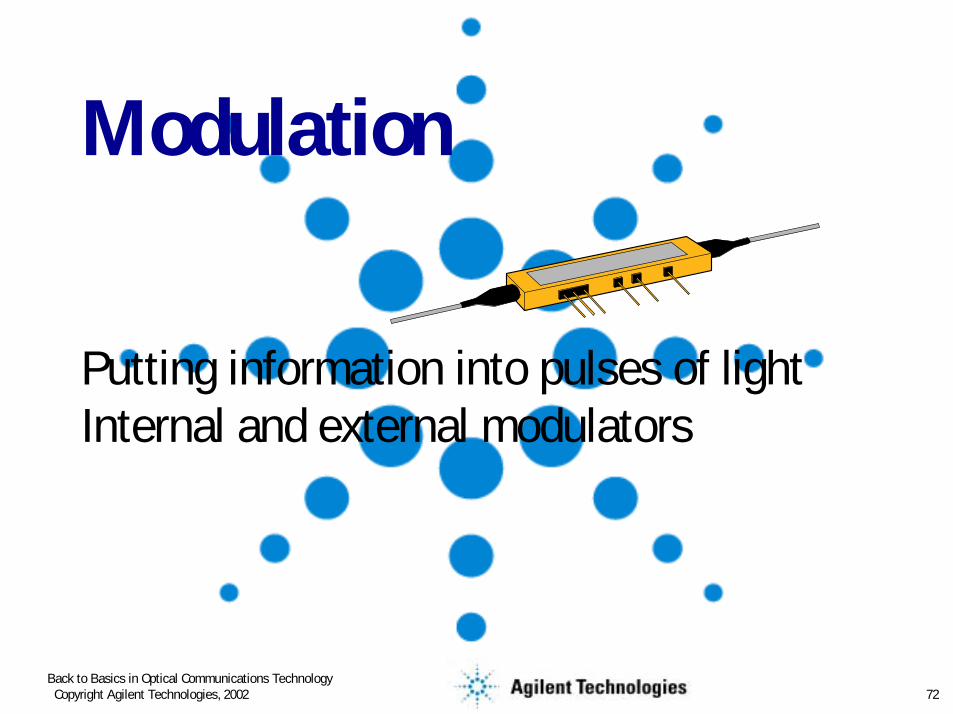
Modulation
Putting information into pulses of lightInternal and external modulators
Back to Basics in Optical Communications TechnologyCopyright Agilent Technologies, 2002 73
DispersionCompensator
DispersionCompensator
OtherSegment
OtherSegment
OtherSegment
OtherSegment
LAN
CrossConnect
(Switch)
Data
λ1
λ2...λn
Data
λ1
λ2...λn
dem
ultip
lexe
r
mul
tiple
xer
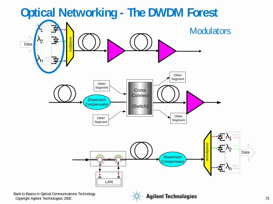
Optical Networking - The DWDM ForestModulators
Back to Basics in Optical Communications TechnologyCopyright Agilent Technologies, 2002 74
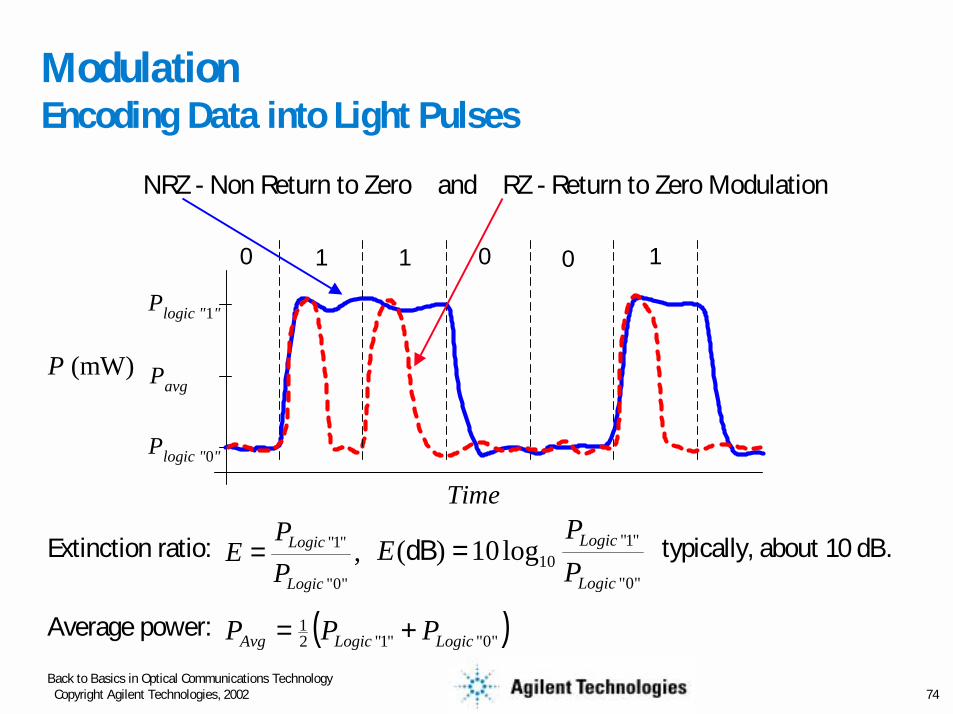
ModulationEncoding Data into Light Pulses
Extinction ratio: typically, about 10 dB.
Average power:
,"0"
"1"
Logic
Logic
PP
E =
( )"0""1"21
LogicLogicAvg PPP +=
"0"
"1"10log10)(
Logic
Logic
PP
E =dB
0 1 1 0 0 1
Time
Plogic "1"
Plogic "0"
PavgP (mW)
NRZ - Non Return to Zero and RZ - Return to Zero Modulation
Back to Basics in Optical Communications TechnologyCopyright Agilent Technologies, 2002 75
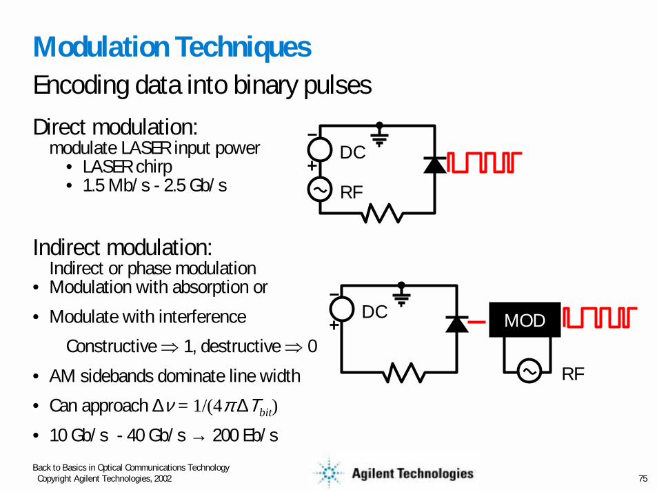
Modulation TechniquesEncoding data into binary pulsesDirect modulation:
modulate LASER input power• LASER chirp • 1.5 Mb/s - 2.5 Gb/s
Indirect modulation:Indirect or phase modulation
• Modulation with absorption or• Modulate with interference
Constructive ⇒ 1, destructive ⇒ 0• AM sidebands dominate line width• Can approach ∆ν = 1/(4π ∆Τbit)• 10 Gb/s - 40 Gb/s → 200 Eb/s
DC
RF
DC MOD
RF
Back to Basics in Optical Communications TechnologyCopyright Agilent Technologies, 2002 76
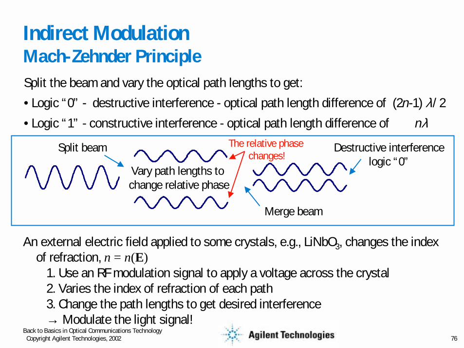
Indirect ModulationMach-Zehnder PrincipleSplit the beam and vary the optical path lengths to get:• Logic “0” - destructive interference - optical path length difference of (2n-1) λ/2 • Logic “1” - constructive interference - optical path length difference of nλ
Vary path lengths to change relative phase
Split beam
Merge beam
Destructive interferencelogic “0”
The relative phase changes!
An external electric field applied to some crystals, e.g., LiNbO3, changes the indexof refraction, n = n(E)
1. Use an RF modulation signal to apply a voltage across the crystal 2. Varies the index of refraction of each path3. Change the path lengths to get desired interference→ Modulate the light signal!
Back to Basics in Optical Communications TechnologyCopyright Agilent Technologies, 2002 77
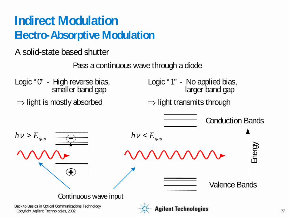
Indirect ModulationElectro-Absorptive ModulationA solid-state based shutter
Pass a continuous wave through a diode
Logic “1” - No applied bias, larger band gap
⇒ light transmits through
Logic “0” - High reverse bias, smaller band gap
⇒ light is mostly absorbed
Ener
gy
Conduction Bands
Valence BandsContinuous wave input
gapEh >ν gapEh <ν
Back to Basics in Optical Communications TechnologyCopyright Agilent Technologies, 2002 78
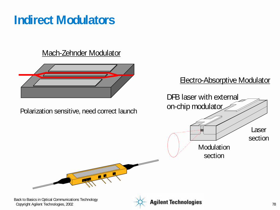
Indirect Modulators
Lasersection
Modulationsection
DFB laser with external on-chip modulatorPolarization sensitive, need correct launch
Mach-Zehnder Modulator
Electro-Absorptive Modulator
Back to Basics in Optical Communications TechnologyCopyright Agilent Technologies, 2002 79
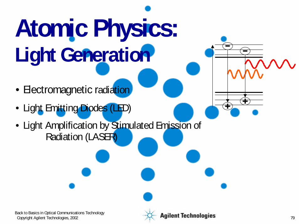
Atomic Physics:Light Generation• Electromagnetic radiation
• Light Emitting Diodes (LED)• Light Amplification by Stimulated Emission of
Radiation (LASER)
Back to Basics in Optical Communications TechnologyCopyright Agilent Technologies, 2002 80
DispersionCompensator
DispersionCompensator
OtherSegment
OtherSegment
OtherSegment
OtherSegment
LAN
CrossConnect
(Switch)
Data
λ1
λ2...λn
Data
λ1
λ2...λn
dem
ultip
lexe
r
mul
tiple
xer
Optical Networking - The DWDM ForestOptical Transmitters
Back to Basics in Optical Communications TechnologyCopyright Agilent Technologies, 2002 81
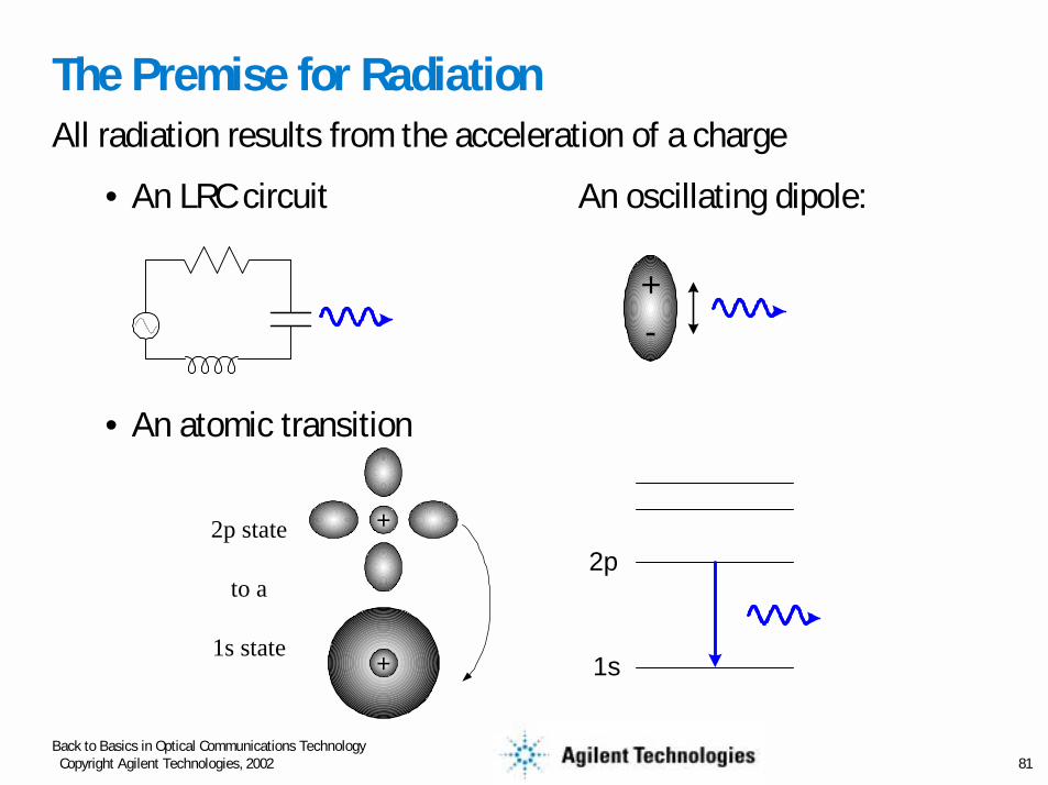
The Premise for RadiationAll radiation results from the acceleration of a charge
• An LRC circuit An oscillating dipole:
• An atomic transition
+
-
+
+
2p state
to a
1s state1s
2p
Back to Basics in Optical Communications TechnologyCopyright Agilent Technologies, 2002 82
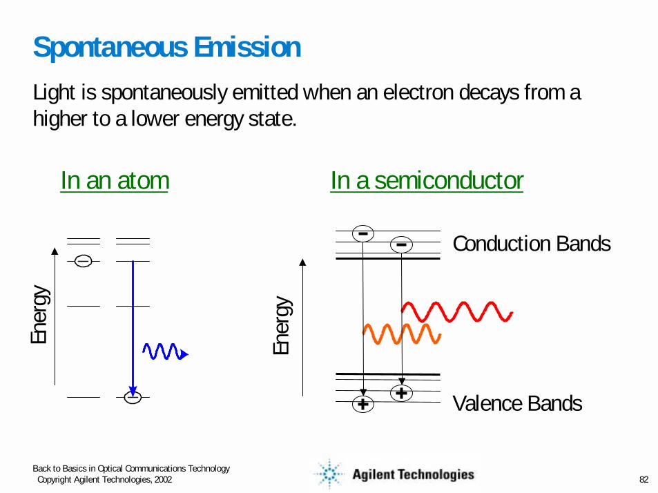
Spontaneous EmissionLight is spontaneously emitted when an electron decays from a higher to a lower energy state.
In an atom In a semiconductor
Ener
gyConduction Bands
Valence Bands
Ener
gy
Back to Basics in Optical Communications TechnologyCopyright Agilent Technologies, 2002 83
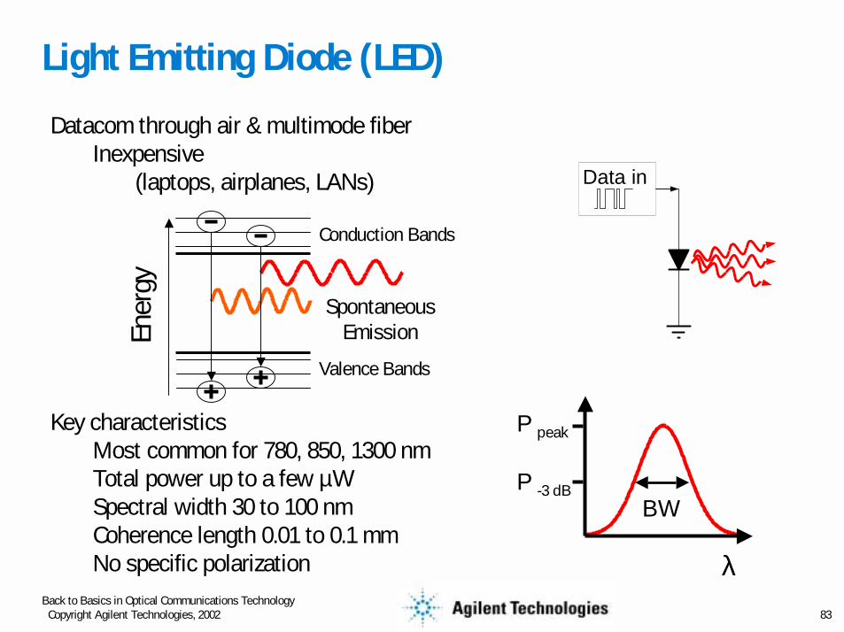
Light Emitting Diode (LED)Datacom through air & multimode fiber
Inexpensive (laptops, airplanes, LANs)
Key characteristicsMost common for 780, 850, 1300 nmTotal power up to a few µWSpectral width 30 to 100 nmCoherence length 0.01 to 0.1 mm No specific polarization
P -3 dB
P peak
BW
Ener
gy
SpontaneousEmission
Conduction Bands
Valence Bands
λ
Data in
Back to Basics in Optical Communications TechnologyCopyright Agilent Technologies, 2002 84
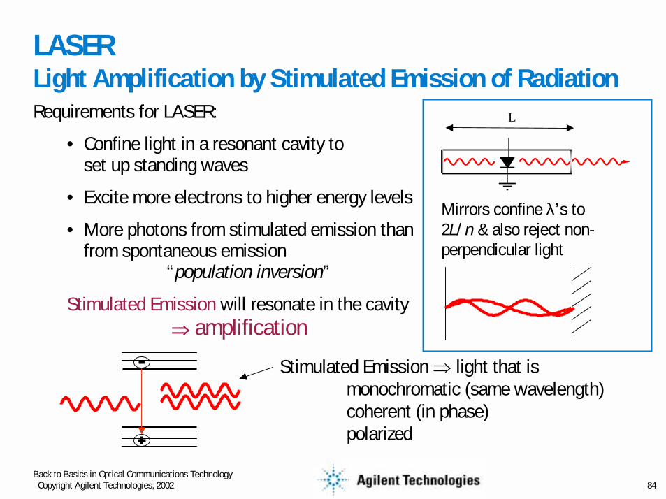
LASERLight Amplification by Stimulated Emission of RadiationRequirements for LASER:
• Confine light in a resonant cavity to set up standing waves
• Excite more electrons to higher energy levels• More photons from stimulated emission than
from spontaneous emission“population inversion”
Stimulated Emission will resonate in the cavity⇒⇒⇒⇒ amplification
Mirrors confine λ’s to2L/n & also reject non-perpendicular light
L
Stimulated Emission ⇒ light that is monochromatic (same wavelength)coherent (in phase)polarized
Back to Basics in Optical Communications TechnologyCopyright Agilent Technologies, 2002 85
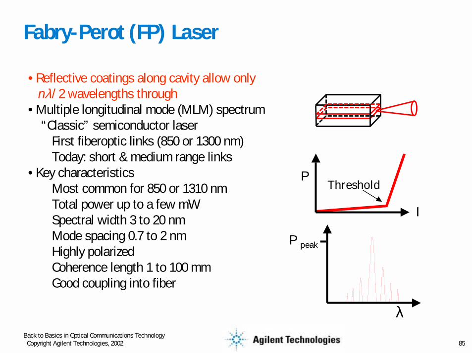
Fabry-Perot (FP) Laser
• Reflective coatings along cavity allow onlynλ/2 wavelengths through
• Multiple longitudinal mode (MLM) spectrum“Classic” semiconductor laser
First fiberoptic links (850 or 1300 nm)Today: short & medium range links
• Key characteristicsMost common for 850 or 1310 nmTotal power up to a few mWSpectral width 3 to 20 nmMode spacing 0.7 to 2 nmHighly polarizedCoherence length 1 to 100 mmGood coupling into fiber
P peak
I
PThreshold
λ
Back to Basics in Optical Communications TechnologyCopyright Agilent Technologies, 2002 86
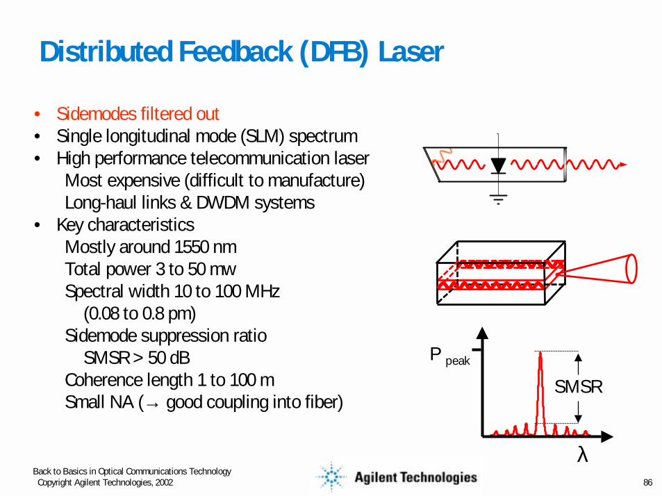
Distributed Feedback (DFB) Laser
• Sidemodes filtered out• Single longitudinal mode (SLM) spectrum• High performance telecommunication laser
Most expensive (difficult to manufacture)Long-haul links & DWDM systems
• Key characteristicsMostly around 1550 nmTotal power 3 to 50 mwSpectral width 10 to 100 MHz
(0.08 to 0.8 pm)Sidemode suppression ratio
SMSR > 50 dBCoherence length 1 to 100 mSmall NA (→ good coupling into fiber)
P peak
SMSR
λ
Back to Basics in Optical Communications TechnologyCopyright Agilent Technologies, 2002 87
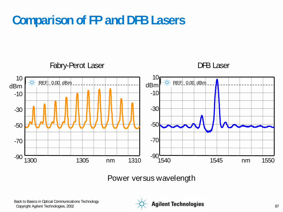
Comparison of FP and DFB Lasers
1300 13101305 nm
REF: 0.00 dBm
-90
-70
-50
-30
-10
10dBm
1540 15501545 nm
REF: 0.00 dBm
-90
-70
-50
-30
-10
10dBm
Power versus wavelength
Fabry-Perot Laser DFB Laser
Back to Basics in Optical Communications TechnologyCopyright Agilent Technologies, 2002 88
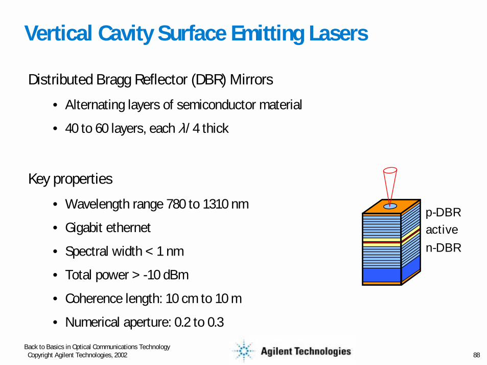
Vertical Cavity Surface Emitting Lasers
Distributed Bragg Reflector (DBR) Mirrors• Alternating layers of semiconductor material• 40 to 60 layers, each λ/4 thick
Key properties• Wavelength range 780 to 1310 nm • Gigabit ethernet • Spectral width < 1 nm• Total power > -10 dBm• Coherence length: 10 cm to 10 m• Numerical aperture: 0.2 to 0.3
active
n-DBR
p-DBR
Back to Basics in Optical Communications TechnologyCopyright Agilent Technologies, 2002 89
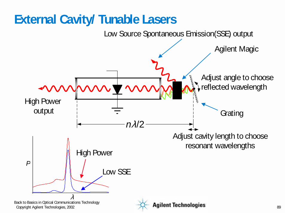
External Cavity/Tunable Lasers
High Power output
Low Source Spontaneous Emission(SSE) output
Adjust angle to choose reflected wavelength
Adjust cavity length to choose resonant wavelengths
Agilent Magic
nλ/2Grating
P
λ
High Power
Low SSE
Back to Basics in Optical Communications TechnologyCopyright Agilent Technologies, 2002 90
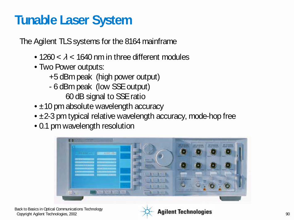
Tunable Laser SystemThe Agilent TLS systems for the 8164 mainframe
• 1260 < λ < 1640 nm in three different modules• Two Power outputs:
+5 dBm peak (high power output)- 6 dBm peak (low SSE output)
60 dB signal to SSE ratio• ±10 pm absolute wavelength accuracy • ±2-3 pm typical relative wavelength accuracy, mode-hop free• 0.1 pm wavelength resolution
Back to Basics in Optical Communications TechnologyCopyright Agilent Technologies, 2002 91
Other Light Sources
Need for small coherence length high power light sources:
White light source• Specialized tungsten light bulb• Wavelength range 900 to 1700 nm, • Power density 0.1 to 0.4 nw/nm (SM), 10 to 25 nw/nm (MM)
Amplified spontaneous emission (ASE) source• “Noise” of an optical amplifier without input signal• Wavelength range 1525 to 1570 nm• Power density 10 to 100 µw/nm
Back to Basics in Optical Communications TechnologyCopyright Agilent Technologies, 2002 92
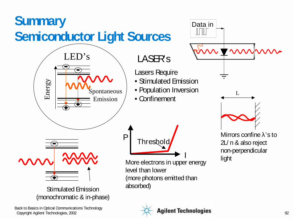
SummarySemiconductor Light Sources
Stimulated Emission(monochromatic & in-phase)
LASER’sLasers Require• Stimulated Emission• Population Inversion• ConfinementEn
ergy
LED’s
SpontaneousEmission
I
P Threshold
More electrons in upper energy level than lower(more photons emitted than absorbed)
Mirrors confine λ’s to2L/n & also reject non-perpendicular light
L
Data in
Back to Basics in Optical Communications TechnologyCopyright Agilent Technologies, 2002 93
Parameters to TestCharacterization of TransmittersOutput Power
• Power meter
Wavelength• Optical Spectrum Analyzer, λaccuracy ~ ± 15 pm, δλ ∼ 50 pm• Interferometer-based wavelength meter, λaccuracy ~ ± 5 pm, δλ ∼ 0.3 pm
Linewidth, chirp, modulation effects, ultra DWDM structure• High Resolution Spectrometer, λaccuracy ~ ± 15 pm, δλ ∼ 8 fm
Distortion, Relative Intensity Noise (RIN), harmonic noise, Spontaneous emission/recombination relaxation effects
• Lightwave Signal Analyzer
Electrical-Optical Response, BandwidthRecombination time scale affects modulation properties
• Lightwave Component Analyzer
Back to Basics in Optical Communications TechnologyCopyright Agilent Technologies, 2002 94
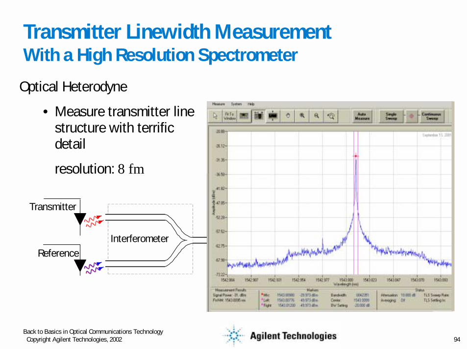
Transmitter Linewidth MeasurementWith a High Resolution Spectrometer
Optical Heterodyne• Measure transmitter line
structure with terrific detailresolution: 8 fm
Transmitter
ReferenceInterferometer
Back to Basics in Optical Communications TechnologyCopyright Agilent Technologies, 2002 95
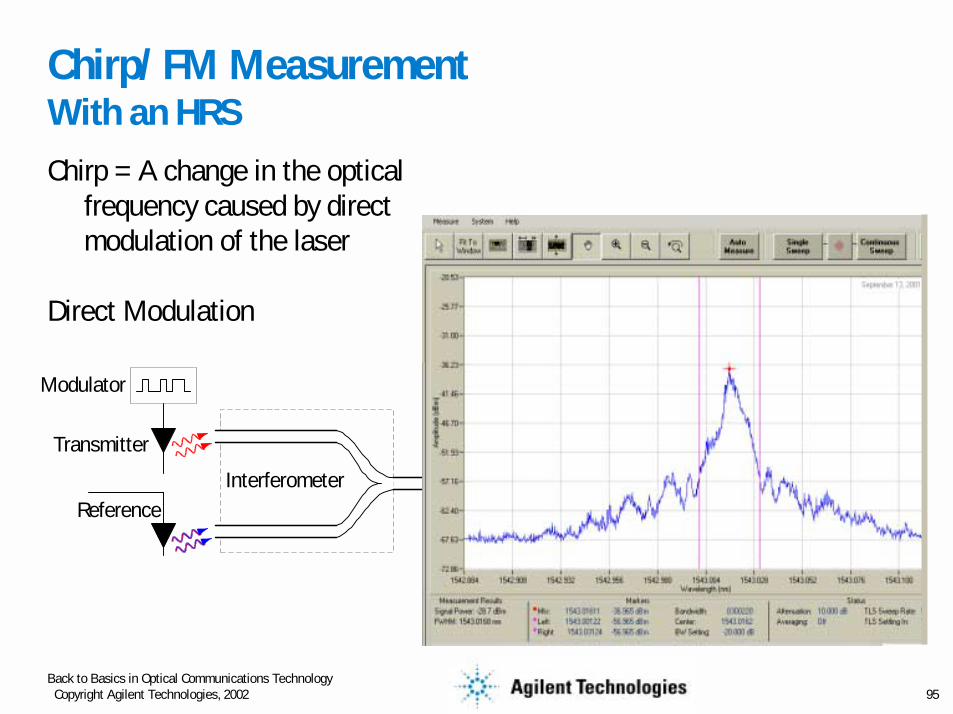
Chirp/FM MeasurementWith an HRSChirp = A change in the optical
frequency caused by directmodulation of the laser
Direct Modulation
Transmitter
ReferenceInterferometer
Modulator
Back to Basics in Optical Communications TechnologyCopyright Agilent Technologies, 2002 96
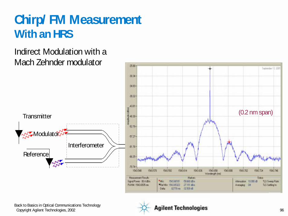
Chirp/FM MeasurementWith an HRSIndirect Modulation with a Mach Zehnder modulator
Transmitter
ReferenceInterferometer
Modulator
(0.2 nm span)
Back to Basics in Optical Communications TechnologyCopyright Agilent Technologies, 2002 97
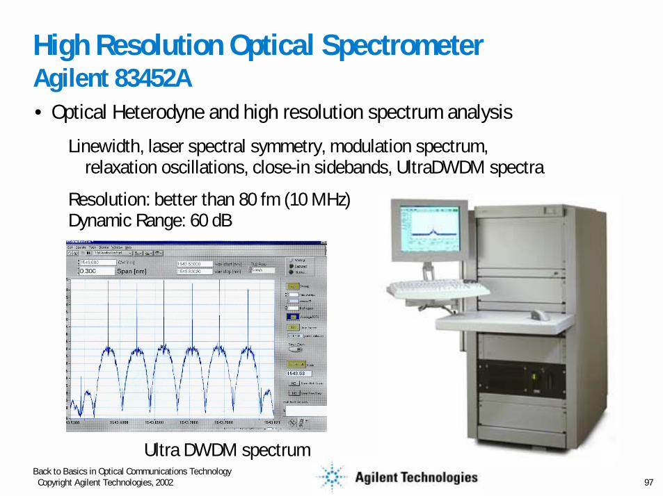
High Resolution Optical Spectrometer Agilent 83452A• Optical Heterodyne and high resolution spectrum analysis
Linewidth, laser spectral symmetry, modulation spectrum, relaxation oscillations, close-in sidebands, UltraDWDM spectra
Resolution: better than 80 fm (10 MHz)Dynamic Range: 60 dB
Ultra DWDM spectrum
Back to Basics in Optical Communications TechnologyCopyright Agilent Technologies, 2002 98
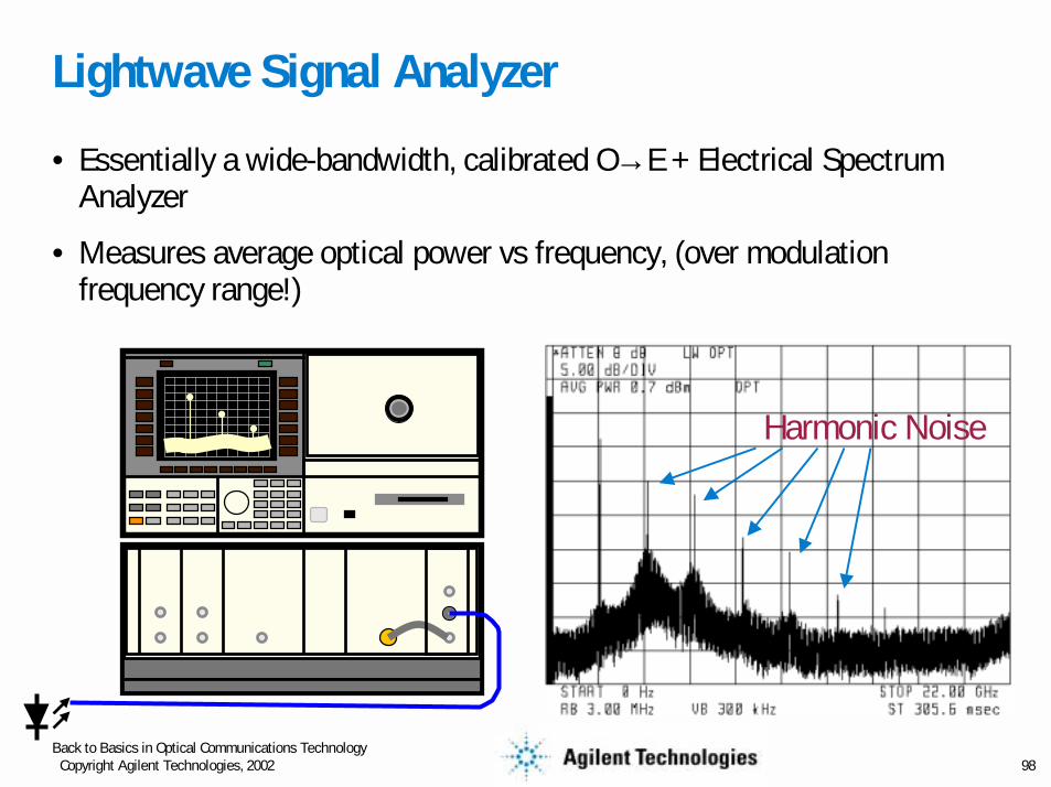
Lightwave Signal Analyzer• Essentially a wide-bandwidth, calibrated O→E + Electrical Spectrum
Analyzer• Measures average optical power vs frequency, (over modulation
frequency range!)
Harmonic Noise
Back to Basics in Optical Communications TechnologyCopyright Agilent Technologies, 2002 99
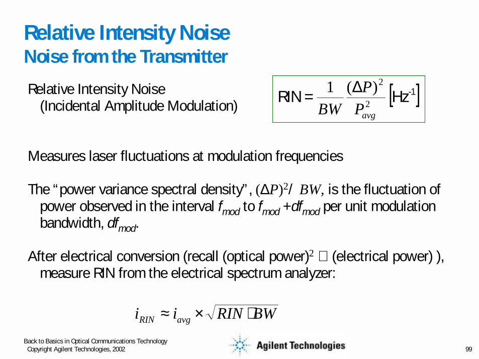
Relative Intensity NoiseNoise from the TransmitterRelative Intensity Noise
(Incidental Amplitude Modulation)
Measures laser fluctuations at modulation frequencies
The “power variance spectral density”, (∆P)2/ BW, is the fluctuation of power observed in the interval fmod to fmod +dfmod per unit modulation bandwidth, dfmod.
After electrical conversion (recall (optical power)2 ∝ (electrical power) ), measure RIN from the electrical spectrum analyzer:
[ ]1-HzRIN 2
2)(1avgPP
BW∆=
BWRINii avgRIN ⋅×≈
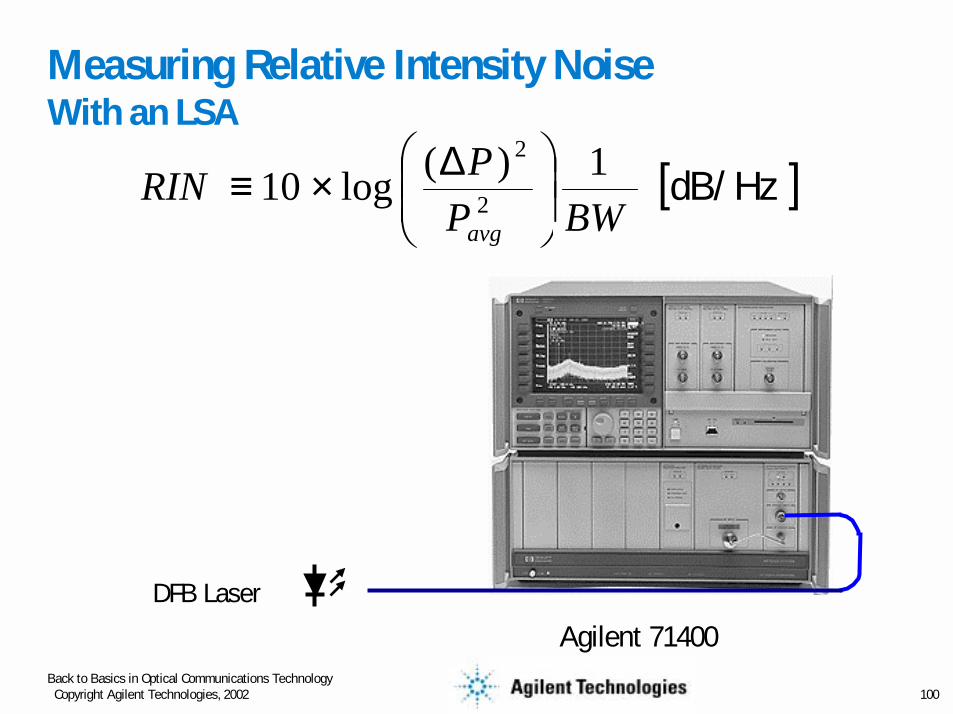
Back to Basics in Optical Communications TechnologyCopyright Agilent Technologies, 2002 100
Measuring Relative Intensity NoiseWith an LSA
DFB Laser
[ ]dB/Hz BWP
PRINavg
1)(log10 2
2
∆×≡
Agilent 71400
Back to Basics in Optical Communications TechnologyCopyright Agilent Technologies, 2002 101
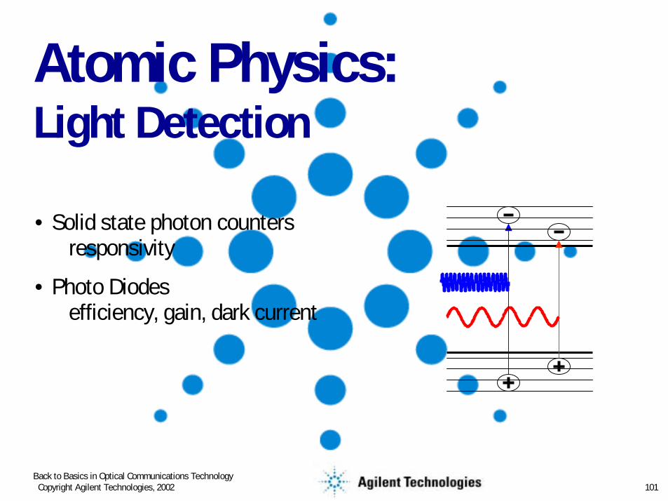
• Solid state photon countersresponsivity
• Photo Diodesefficiency, gain, dark current
Atomic Physics:Light Detection
Back to Basics in Optical Communications TechnologyCopyright Agilent Technologies, 2002 102
DispersionCompensator
DispersionCompensator
OtherSegment
OtherSegment
OtherSegment
OtherSegment
LAN
CrossConnect
(Switch)
Data
λ1
λ2...λn
Data
λ1
λ2...λn
dem
ultip
lexe
r
mul
tiple
xer
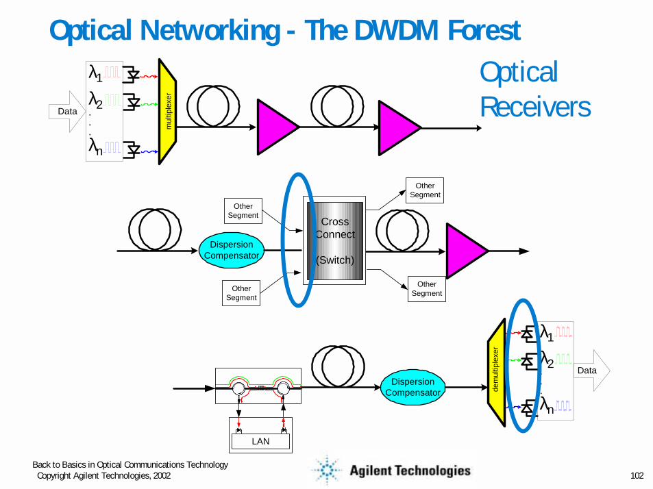
Optical Networking - The DWDM ForestOptical Receivers
Back to Basics in Optical Communications TechnologyCopyright Agilent Technologies, 2002 103
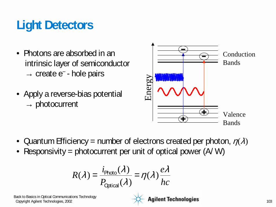
Light Detectors
Valence Bands
Conduction Bands
Ener
gy
• Photons are absorbed in an intrinsic layer of semiconductor→ create e− - hole pairs
• Apply a reverse-bias potential→ photocurrent
• Quantum Efficiency = number of electrons created per photon, η(λ)• Responsivity = photocurrent per unit of optical power (A/W)
hce
PiR λλη
λλλ )(
)()()( ==
Optical
Photo
Back to Basics in Optical Communications TechnologyCopyright Agilent Technologies, 2002 104
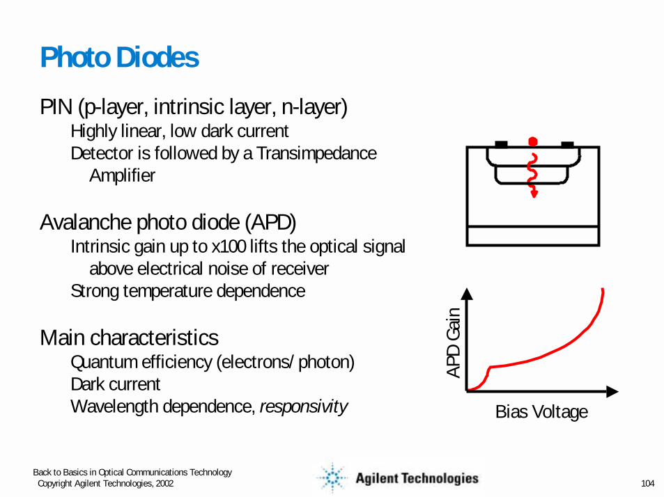
Photo DiodesPIN (p-layer, intrinsic layer, n-layer)
Highly linear, low dark currentDetector is followed by a Transimpedance
Amplifier
Avalanche photo diode (APD)Intrinsic gain up to x100 lifts the optical signal
above electrical noise of receiverStrong temperature dependence
Main characteristicsQuantum efficiency (electrons/photon)Dark currentWavelength dependence, responsivity
n+
Bias Voltage
APD
Gain
Back to Basics in Optical Communications TechnologyCopyright Agilent Technologies, 2002 105
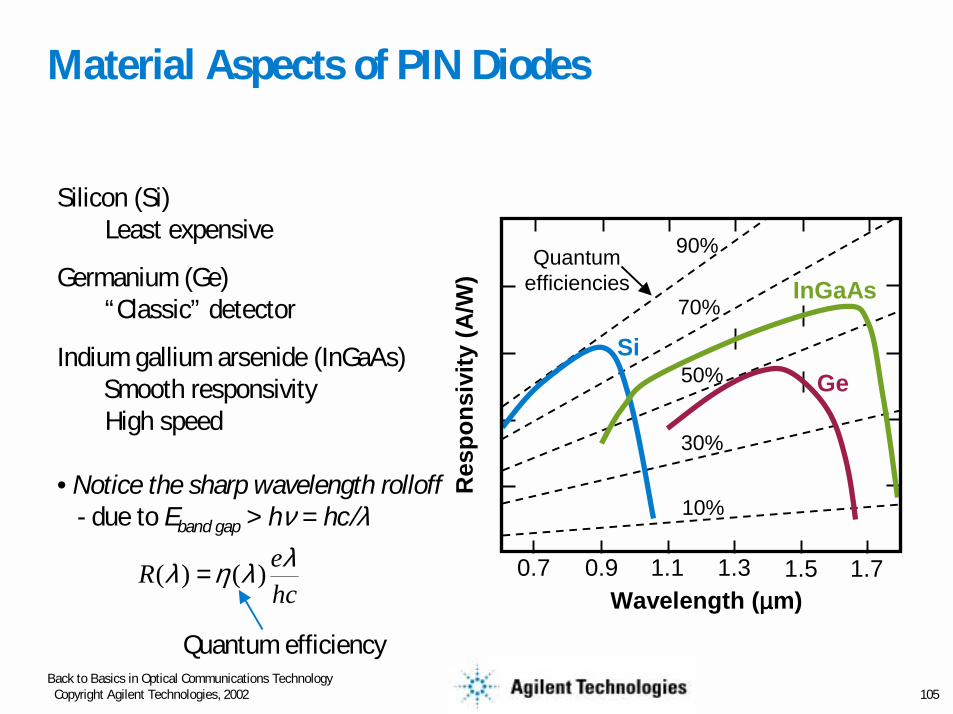
Material Aspects of PIN Diodes
Silicon (Si)Least expensive
Germanium (Ge) “Classic” detector
Indium gallium arsenide (InGaAs) Smooth responsivityHigh speed
• Notice the sharp wavelength rolloff - due to Eband gap > hν = hc/λ
0.7 0.9 1.1 1.3 1.5 1.7
90%
70%
50%
30%
10%
Quantumefficiencies
Si
InGaAs
Ge
Wavelength (µµµµm)
Res
pons
ivity
(A/W
)
hceR λληλ )()( =
Quantum efficiency
Back to Basics in Optical Communications TechnologyCopyright Agilent Technologies, 2002 106
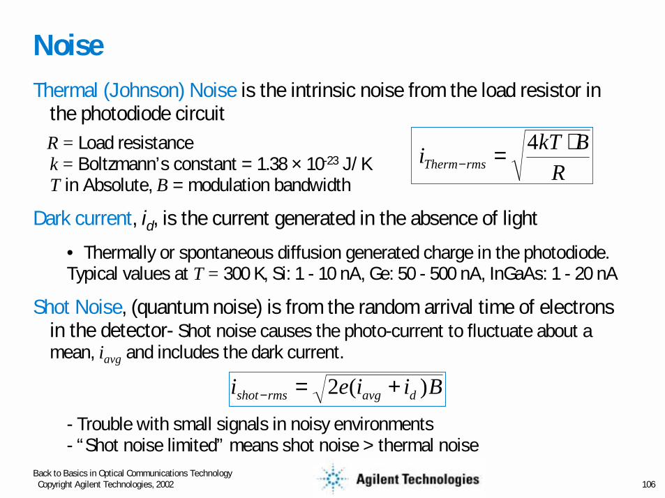
NoiseThermal (Johnson) Noise is the intrinsic noise from the load resistor in
the photodiode circuitR = Load resistancek = Boltzmann’s constant = 1.38 × 10⁻²³ J/KT in Absolute, B = modulation bandwidth R
BkTi rmsTherm⋅=−
4
Dark current, id, is the current generated in the absence of light• Thermally or spontaneous diffusion generated charge in the photodiode.Typical values at T = 300 K, Si: 1 - 10 nA, Ge: 50 - 500 nA, InGaAs: 1 - 20 nA
Shot Noise, (quantum noise) is from the random arrival time of electrons in the detector- Shot noise causes the photo-current to fluctuate about a mean, iavg and includes the dark current.
- Trouble with small signals in noisy environments- “Shot noise limited” means shot noise > thermal noise
Biiei davgrmsshot )(2 +=−
Back to Basics in Optical Communications TechnologyCopyright Agilent Technologies, 2002 107
Receivers:Sensitivity and Modulation Bandwidth
High sensitivity requires a large/deep detector• Need to detect each photon = increase quantum efficiency
• create more electron-hole pairs and catch each one
Large Bandwidth requires a small/shallow detector• Need to finish detection process fast to accommodate a short pulse
Larger the detector the longer the “relaxation time” of the detection process
→→→→ Tradeoff between sensitivity and bandwidth:Larger bandwidth, lower sensitivity
Example: Sensitivity Modulation rateLightwave Clock/Data Receivers: Agilent 83446A -28 dBm 2.5 Gb/s
Agilent 83434A -16 dBm 10 Gb/s
Back to Basics in Optical Communications TechnologyCopyright Agilent Technologies, 2002 108
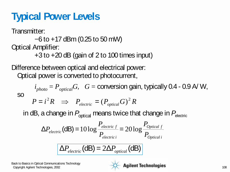
Typical Power LevelsTransmitter:
−6 to +17 dBm (0.25 to 50 mW)Optical Amplifier:
+3 to +20 dB (gain of 2 to 100 times input)Difference between optical and electrical power:
Optical power is converted to photocurrent,iphoto = PopticalG, G = conversion gain, typically 0.4 - 0.9 A/W,
so
in dB, a change in Poptical means twice that change in Pelectric
RGPPRiP opticalelectric22 )(=⇒=
(dB)(dB) opticalelectric PP ∆=∆ 2iOptical
fOptical
ielectric
felectricelectric P
PPP
P
(dB) log20log10 ==∆
Back to Basics in Optical Communications TechnologyCopyright Agilent Technologies, 2002 109
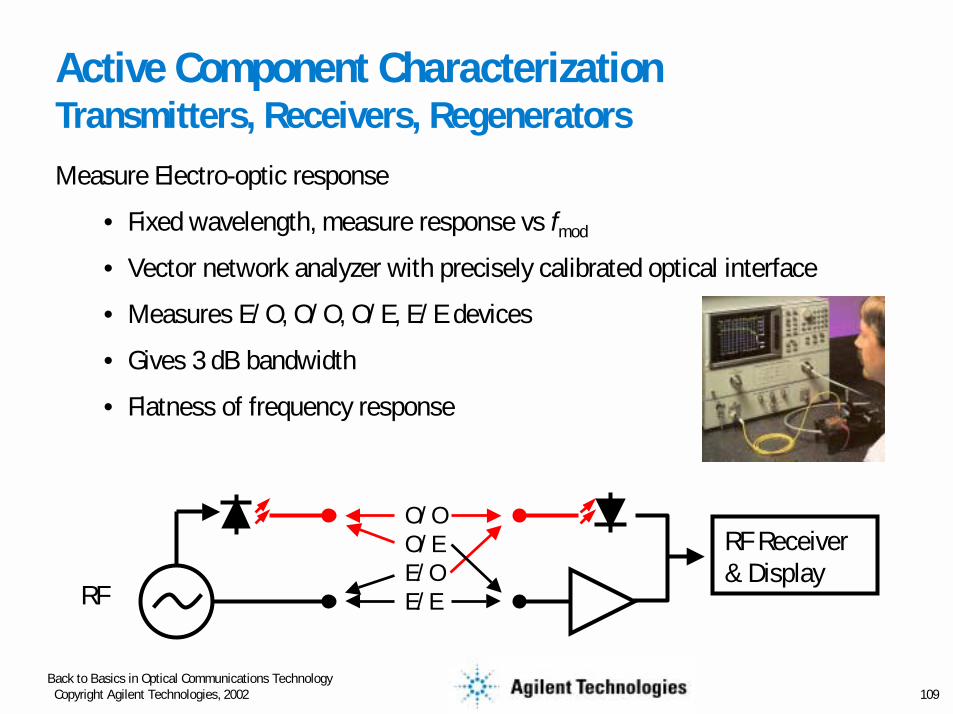
Active Component CharacterizationTransmitters, Receivers, RegeneratorsMeasure Electro-optic response
• Fixed wavelength, measure response vs fmod
• Vector network analyzer with precisely calibrated optical interface• Measures E/O, O/O, O/E, E/E devices• Gives 3 dB bandwidth• Flatness of frequency response
RF Receiver & Display
O/OO/EE/OE/ERF
Back to Basics in Optical Communications TechnologyCopyright Agilent Technologies, 2002 110
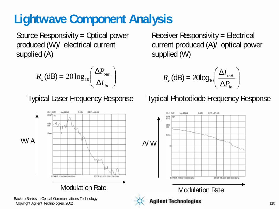
Lightwave Component AnalysisSource Responsivity = Optical power produced (W)/ electrical current supplied (A)
Receiver Responsivity = Electrical current produced (A)/ optical power supplied (W)
Modulation Rate Modulation Rate
W/A A/W
∆∆
=in
outs I
PR 10log20(dB)
∆∆
=in
outr P
IR 1020log(dB)
Typical Laser Frequency Response Typical Photodiode Frequency Response
Back to Basics in Optical Communications TechnologyCopyright Agilent Technologies, 2002 111
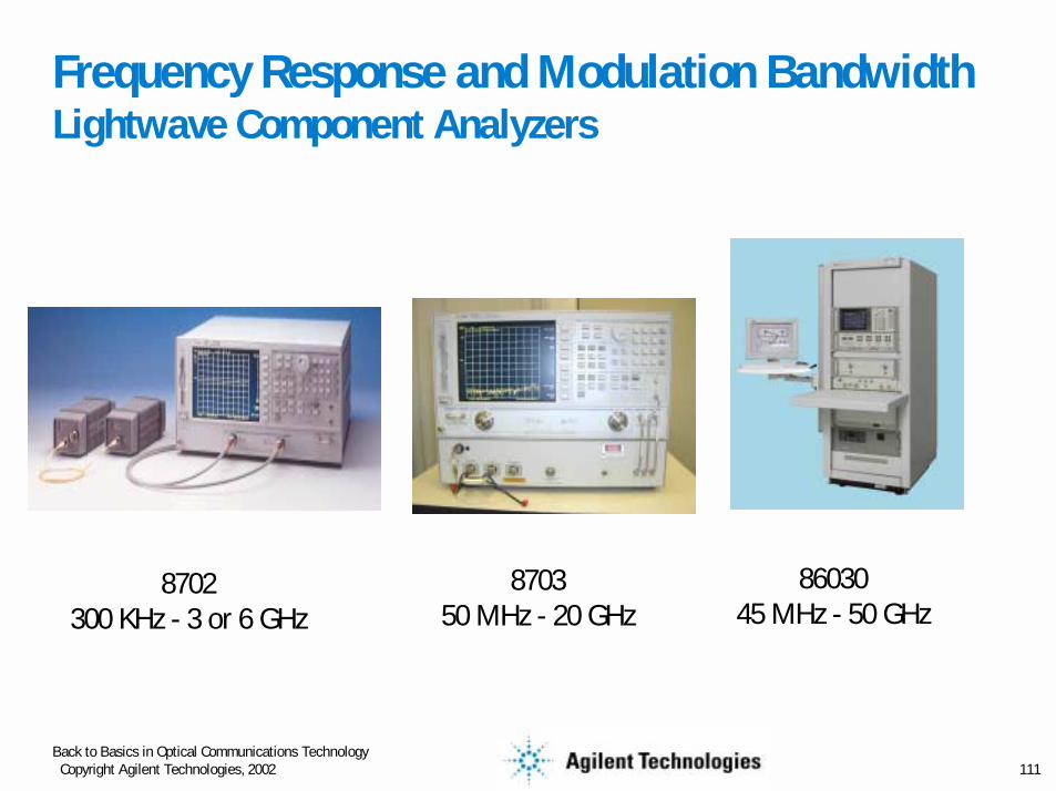
Frequency Response and Modulation Bandwidth Lightwave Component Analyzers
8702300 KHz - 3 or 6 GHz
870350 MHz - 20 GHz
8603045 MHz - 50 GHz
Back to Basics in Optical Communications TechnologyCopyright Agilent Technologies, 2002 112
DispersionCompensator
DispersionCompensator
OtherSegment
OtherSegment
OtherSegment
OtherSegment
LAN
CrossConnect
(Switch)
Data
λ1
λ2...λn
Data
λ1
λ2...λn
dem
ultip
lexe
r
mul
tiple
xer
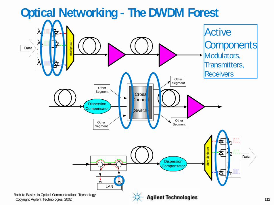
Optical Networking - The DWDM ForestActive ComponentsModulators,Transmitters,Receivers
Back to Basics in Optical Communications TechnologyCopyright Agilent Technologies, 2002 113
Optical Signal Amplification
andDWDM
Back to Basics in Optical Communications TechnologyCopyright Agilent Technologies, 2002 114
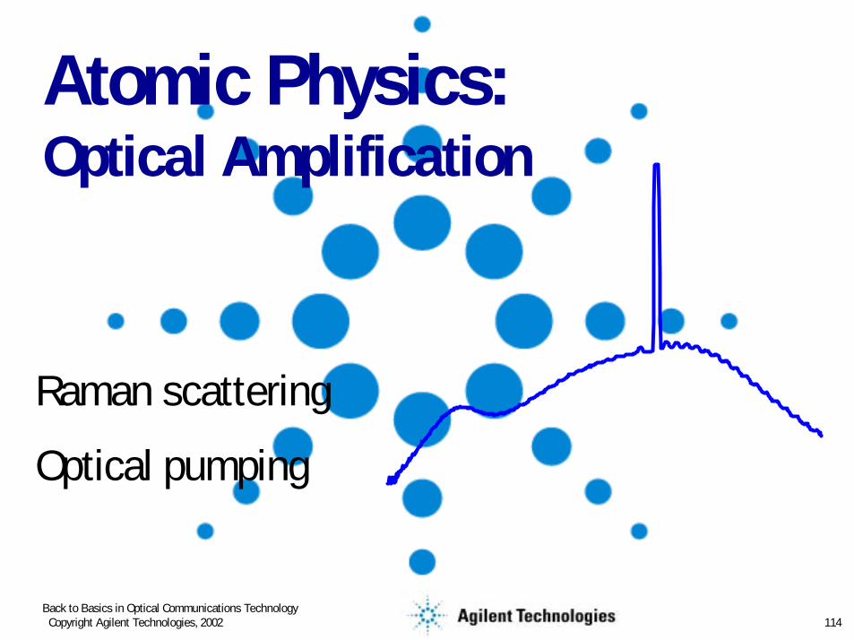
Raman scatteringOptical pumping
Atomic Physics:Optical Amplification
Back to Basics in Optical Communications TechnologyCopyright Agilent Technologies, 2002 115
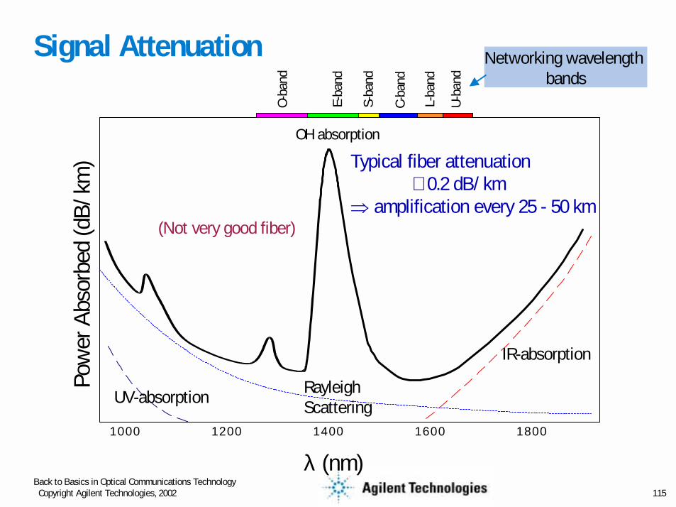
Signal AttenuationPo
wer A
bsor
bed
(dB/
km)
1200 1400 16001000 1800
OH absorption
λ (nm)
O-ba
nd
E-ba
nd
S-ba
nd
C-ba
nd
L-ba
nd
U-ba
nd
UV-absorption
IR-absorption
RayleighScattering
Typical fiber attenuation≅ 0.2 dB/km
⇒ amplification every 25 - 50 km(Not very good fiber)
Networking wavelength bands
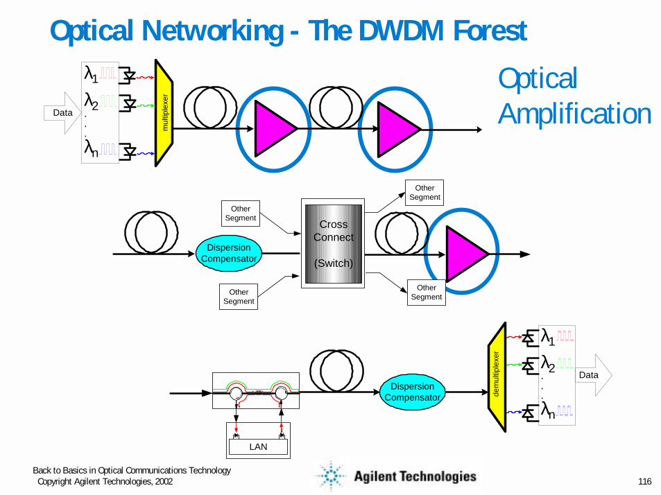
Back to Basics in Optical Communications TechnologyCopyright Agilent Technologies, 2002 116
Optical Networking - The DWDM ForestOptical Amplification
DispersionCompensator
DispersionCompensator
OtherSegment
OtherSegment
OtherSegment
OtherSegment
LAN
CrossConnect
(Switch)
Data
λ1
λ2...λn
Data
λ1
λ2...λn
dem
ultip
lexe
r
mul
tiple
xer
Back to Basics in Optical Communications TechnologyCopyright Agilent Technologies, 2002 117
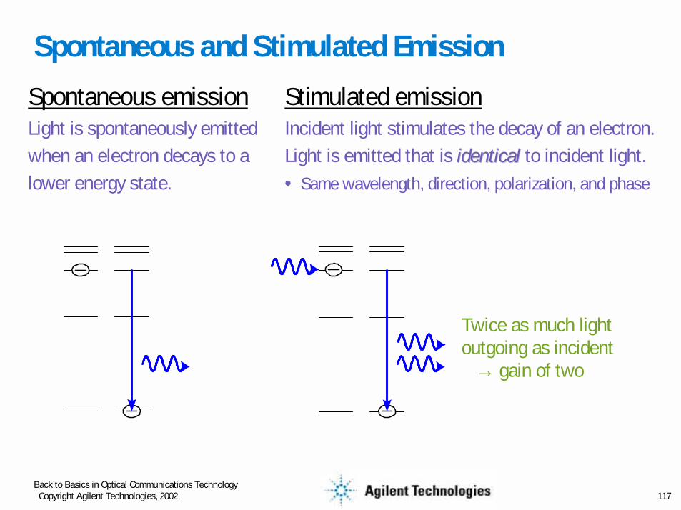
Spontaneous and Stimulated EmissionSpontaneous emissionLight is spontaneously emitted when an electron decays to a lower energy state.
Stimulated emissionIncident light stimulates the decay of an electron.Light is emitted that is identicalidentical to incident light.• Same wavelength, direction, polarization, and phase
Twice as much lightoutgoing as incident
→ gain of two
Back to Basics in Optical Communications TechnologyCopyright Agilent Technologies, 2002 118
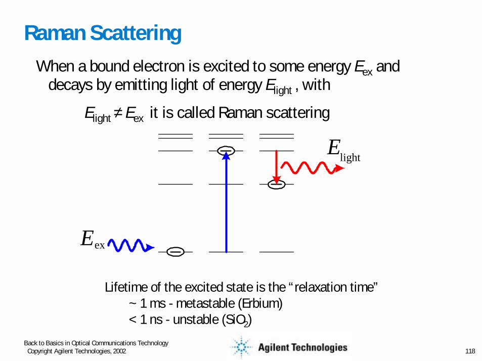
Raman ScatteringWhen a bound electron is excited to some energy Eex and
decays by emitting light of energy Elight , withElight ≠ Eex it is called Raman scattering
E
lightE
ex
Lifetime of the excited state is the “relaxation time”~ 1 ms - metastable (Erbium)< 1 ns - unstable (SiO2)
Back to Basics in Optical Communications TechnologyCopyright Agilent Technologies, 2002 119
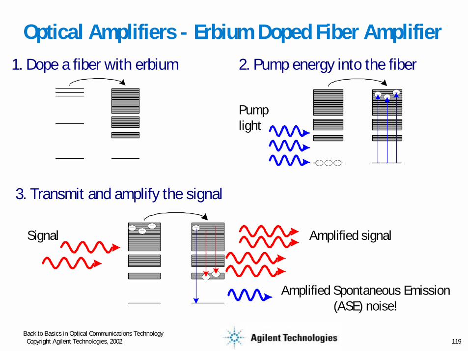
Optical Amplifiers - Erbium Doped Fiber Amplifier1. Dope a fiber with erbium 2. Pump energy into the fiber
3. Transmit and amplify the signal
Amplified signalSignal
Pump light
Amplified Spontaneous Emission(ASE) noise!
Back to Basics in Optical Communications TechnologyCopyright Agilent Technologies, 2002 120
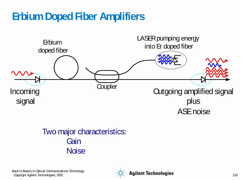
Erbium Doped Fiber Amplifiers
Erbium doped fiber
LASER pumping energy into Er doped fiber
Incoming signal
Outgoing amplified signalplus
Coupler
ASE noise
Two major characteristics:Gain Noise
Back to Basics in Optical Communications TechnologyCopyright Agilent Technologies, 2002 121
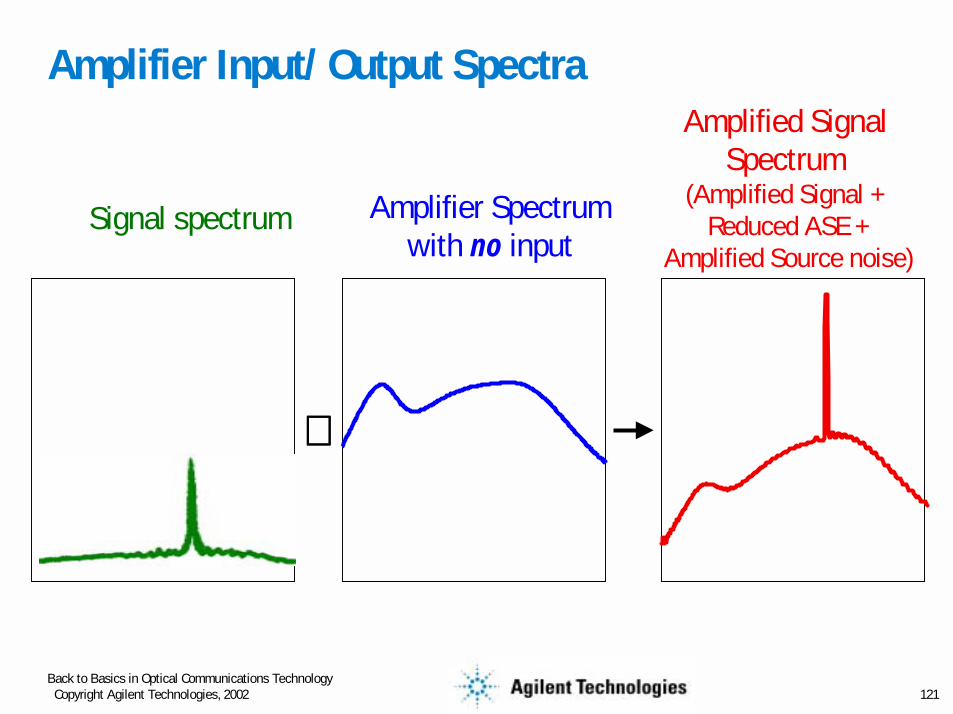
Amplifier Input/Output Spectra
Signal spectrum Amplifier Spectrum with no input
Amplified Signal Spectrum
(Amplified Signal +Reduced ASE +
Amplified Source noise)
⊗⊗⊗⊗
Back to Basics in Optical Communications TechnologyCopyright Agilent Technologies, 2002 122
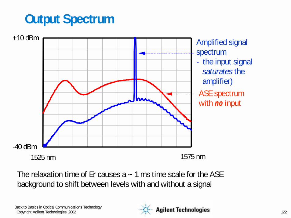
Output Spectrum
ASE spectrum with no input
1575 nm-40 dBm
1525 nm
+10 dBm Amplified signal spectrum - the input signal
saturates the amplifier)
The relaxation time of Er causes a ~ 1 ms time scale for the ASE background to shift between levels with and without a signal
Back to Basics in Optical Communications TechnologyCopyright Agilent Technologies, 2002 123
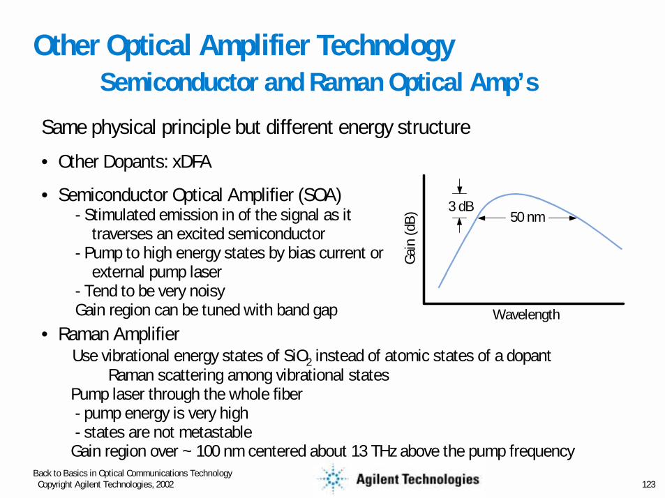
Other Optical Amplifier TechnologySemiconductor and Raman Optical Amp’s
Same physical principle but different energy structure• Other Dopants: xDFA
50 nm3 dB
Wavelength
Gain
(dB)
• Raman AmplifierUse vibrational energy states of SiO2 instead of atomic states of a dopant
Raman scattering among vibrational statesPump laser through the whole fiber- pump energy is very high- states are not metastable
Gain region over ~ 100 nm centered about 13 THz above the pump frequency
• Semiconductor Optical Amplifier (SOA)- Stimulated emission in of the signal as it
traverses an excited semiconductor- Pump to high energy states by bias current or
external pump laser- Tend to be very noisyGain region can be tuned with band gap
Back to Basics in Optical Communications TechnologyCopyright Agilent Technologies, 2002 124
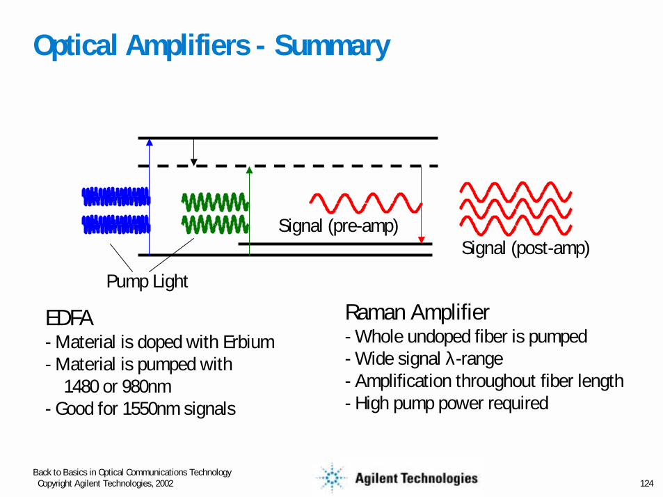
Optical Amplifiers - Summary
EDFA- Material is doped with Erbium- Material is pumped with
1480 or 980nm- Good for 1550nm signals
Pump Light
Signal (pre-amp)Signal (post-amp)
Raman Amplifier- Whole undoped fiber is pumped- Wide signal λ-range- Amplification throughout fiber length- High pump power required
Back to Basics in Optical Communications TechnologyCopyright Agilent Technologies, 2002 125
DWDMDense
WavelengthDivision
Multiplexing
Back to Basics in Optical Communications TechnologyCopyright Agilent Technologies, 2002 126
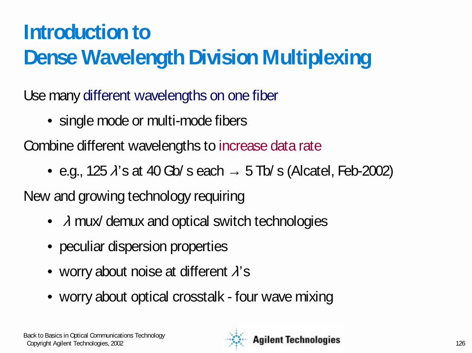
Introduction to Dense Wavelength Division MultiplexingUse many different wavelengths on one fiber
• single mode or multi-mode fibersCombine different wavelengths to increase data rate
• e.g., 125 λ’s at 40 Gb/s each → 5 Tb/s (Alcatel, Feb-2002)New and growing technology requiring
• λ mux/demux and optical switch technologies• peculiar dispersion properties• worry about noise at different λ’s• worry about optical crosstalk - four wave mixing
Back to Basics in Optical Communications TechnologyCopyright Agilent Technologies, 2002 127
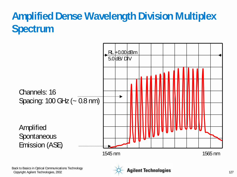
1565 nm
RL +0.00 dBm5.0 dB/DIV
1545 nm
AmplifiedSpontaneousEmission (ASE)
Channels: 16Spacing: 100 GHz (~ 0.8 nm)
Amplified Dense Wavelength Division Multiplex Spectrum
Back to Basics in Optical Communications TechnologyCopyright Agilent Technologies, 2002 128
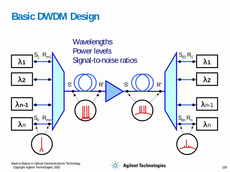
Basic DWDM Design
WavelengthsPower levelsSignal-to-noise ratios
λλλλ2
λλλλn
λλλλ1
λλλλn-1
λλλλ2
λλλλn
λλλλ1
λλλλn-1
S’
Rm1
Sdn Rn
S1
R’S’ R’
R1Sd1
Sn Rmn
Back to Basics in Optical Communications TechnologyCopyright Agilent Technologies, 2002 129
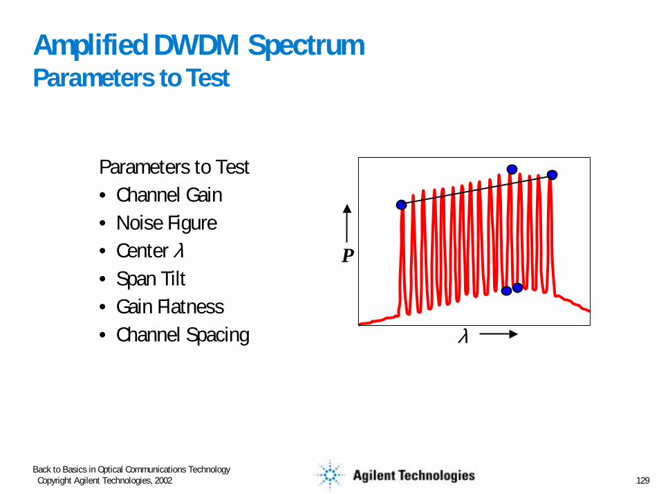
Amplified DWDM SpectrumParameters to Test
P
λ
Parameters to Test• Channel Gain• Noise Figure• Center λ• Span Tilt• Gain Flatness• Channel Spacing
Back to Basics in Optical Communications TechnologyCopyright Agilent Technologies, 2002 130
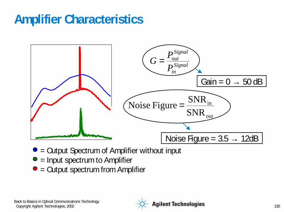
Amplifier Characteristics
out
in
SNRSNRFigure Noise =
Signalin
Signalout
PPG =
Gain = 0 → 50 dB
Noise Figure = 3.5 → 12dB= Output Spectrum of Amplifier without input= Input spectrum to Amplifier= Output spectrum from Amplifier
Back to Basics in Optical Communications TechnologyCopyright Agilent Technologies, 2002 131
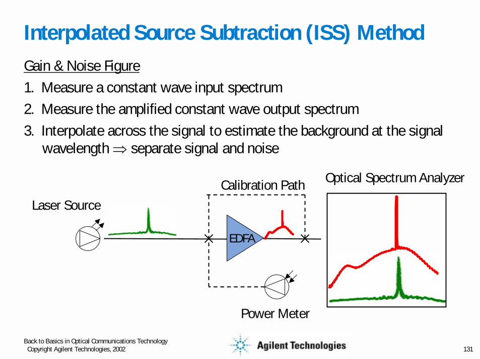
Interpolated Source Subtraction (ISS) Method
EDFA
Optical Spectrum Analyzer
Power Meter
Calibration PathLaser Source
Gain & Noise Figure1. Measure a constant wave input spectrum2. Measure the amplified constant wave output spectrum3. Interpolate across the signal to estimate the background at the signal
wavelength ⇒ separate signal and noise
Back to Basics in Optical Communications TechnologyCopyright Agilent Technologies, 2002 132
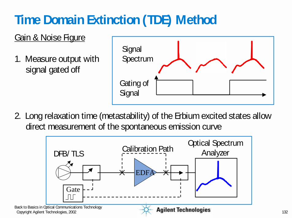
Time Domain Extinction (TDE) Method
EDFA
Optical SpectrumAnalyzerDFB/TLS
Gate
Signal Spectrum
Gating of Signal
Calibration Path
Gain & Noise Figure
1. Measure output with signal gated off
2. Long relaxation time (metastability) of the Erbium excited states allow direct measurement of the spontaneous emission curve
Back to Basics in Optical Communications TechnologyCopyright Agilent Technologies, 2002 133
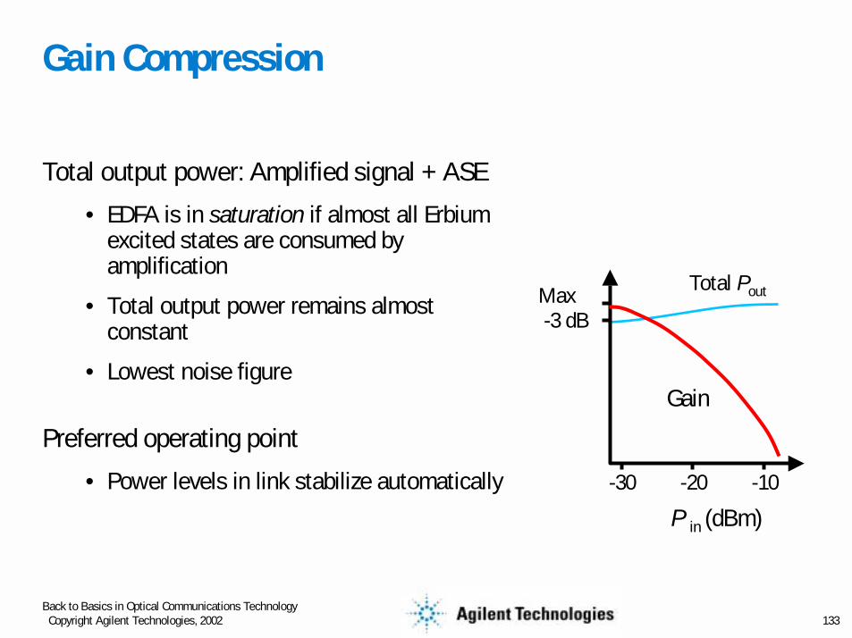
Gain Compression
Total output power: Amplified signal + ASE• EDFA is in saturation if almost all Erbium
excited states are consumed by amplification
• Total output power remains almost constant
• Lowest noise figure
Preferred operating point• Power levels in link stabilize automatically
P in (dBm)
Total Pout
-3 dBMax
-20-30 -10
Gain
Back to Basics in Optical Communications TechnologyCopyright Agilent Technologies, 2002 134
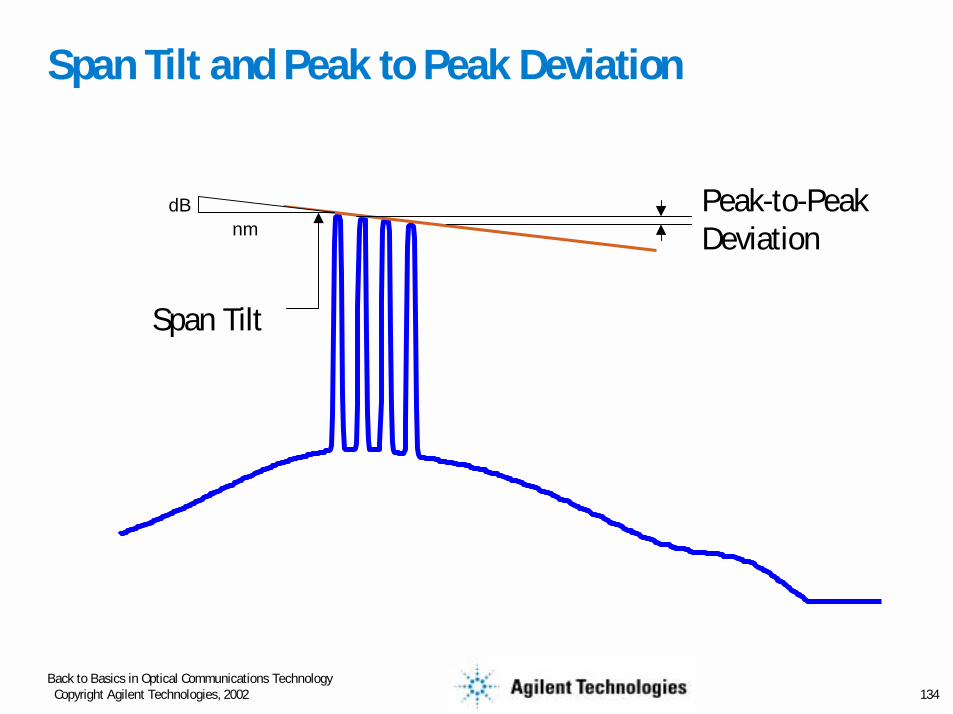
Span Tilt and Peak to Peak Deviation
dBnm
Span Tilt
Peak-to-Peak Deviation
Back to Basics in Optical Communications TechnologyCopyright Agilent Technologies, 2002 135
Characterizing Semiconductor and Raman AmplifiersErbium Doped Fiber Amplifiers (EDFAs) use energy levels that are
metastable states, ∆T~ 1 ms, a long time compared to fmod.Semiconductor and Raman Amplifiers use unstable states:
∆TRaman ~ 0.005 ps and ∆TSOA ~ 1 ns• Time Domain Extinction methods are not useful• Limited to Interpolated Source Subtraction (ISS) for measuring gain and
noise figure
The gain of Raman and semiconductor amplifiers depend strongly on signal polarization, EDFA only weakly.
• Measure gain and noise figure as a function of signal polarization
Back to Basics in Optical Communications TechnologyCopyright Agilent Technologies, 2002 136
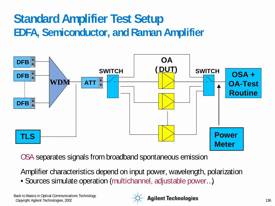
Standard Amplifier Test SetupEDFA, Semiconductor, and Raman Amplifier
OA(DUT)
DFB
DFB
DFB
OSA +OA-TestRoutine
ATT
SWITCH SWITCH
WDM
TLS Power Meter
OSA separates signals from broadband spontaneous emission
Amplifier characteristics depend on input power, wavelength, polarization• Sources simulate operation (multichannel, adjustable power…)
Back to Basics in Optical Communications TechnologyCopyright Agilent Technologies, 2002 137
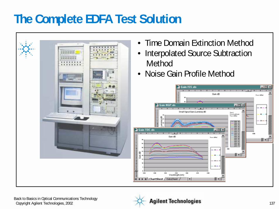
The Complete EDFA Test Solution
• Time Domain Extinction Method• Interpolated Source Subtraction
Method• Noise Gain Profile Method
Back to Basics in Optical Communications TechnologyCopyright Agilent Technologies, 2002 138
Issues in DWDMSM fiber can tolerate up to 50 mW (+17 dBm)
• Nonlinear effects start causing trouble around 10 dBm• About 100 kW/m2 !• limits available channel power to Power/channel < 50 mW/Nchannels
Optical Amplifiers have limited effective λ range• e.g., EDFA: 1525 < λ < 1565 (roughly)
High power densities cause nonlinear scattering• e.g., Kerr effect: n = n(E)⇒ Four Wave Mixing (FWM), self-phase modulation, . . ., noise
Trends:Higher capacity
• 160 wavelengths• 12.5 GHz spacing
All optical network (the grail)
Back to Basics in Optical Communications TechnologyCopyright Agilent Technologies, 2002 139
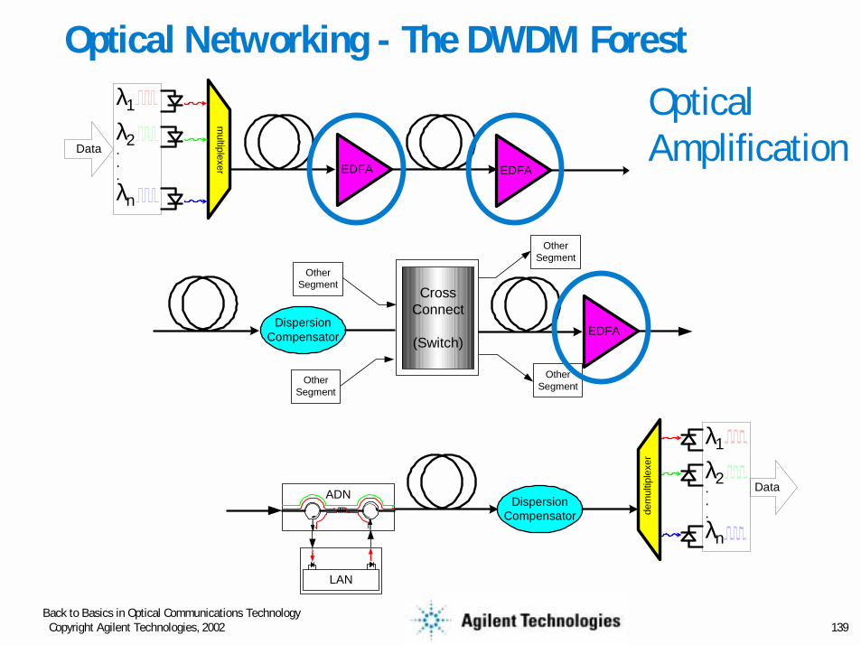
Optical Networking - The DWDM Forest
DispersionCompensator
DispersionCompensator
EDFA
OtherSegment
OtherSegment
OtherSegment
OtherSegment
ADN
LAN
EDFA
CrossConnect
(Switch)
Data
λ1
λ2...λn
multiplexer
Data
λ1
λ2...λn
dem
ultip
lexe
r
EDFA
Optical Amplification
Back to Basics in Optical Communications TechnologyCopyright Agilent Technologies, 2002 140
Dispersion:The evolution of the index of
refraction with wavelength and polarization
Back to Basics in Optical Communications TechnologyCopyright Agilent Technologies, 2002 141
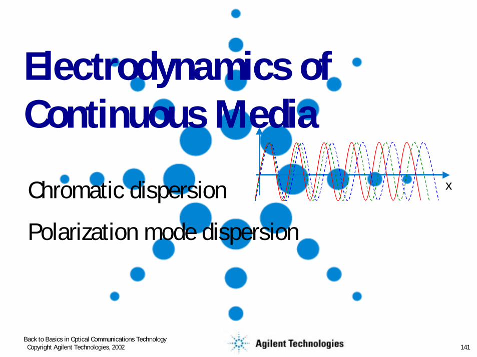
Electrodynamics of Continuous MediaChromatic dispersionPolarization mode dispersion
x

Back to Basics in Optical Communications TechnologyCopyright Agilent Technologies, 2002 142
Optical Networking - The DWDM ForestDispersion Compensators
DispersionCompensator
DispersionCompensator
OtherSegment
OtherSegment
OtherSegment
OtherSegment
LAN
CrossConnect
(Switch)
Data
λ1
λ2...λn
Data
λ1
λ2...λn
dem
ultip
lexe
r
mul
tiple
xer
Back to Basics in Optical Communications TechnologyCopyright Agilent Technologies, 2002 143
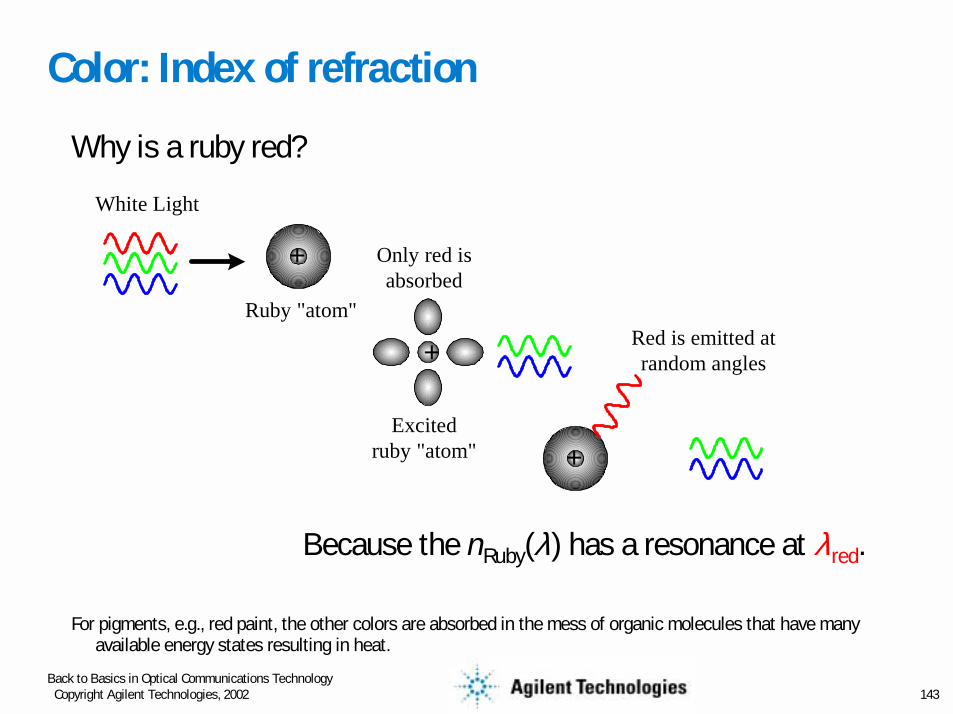
Color: Index of refractionWhy is a ruby red?
Because the nRuby(λ) has a resonance at λred.
For pigments, e.g., red paint, the other colors are absorbed in the mess of organic molecules that have many available energy states resulting in heat.
White Light
+
+
+
Only red isabsorbed
Red is emitted atrandom angles
Ruby "atom"
Excitedruby "atom"
Back to Basics in Optical Communications TechnologyCopyright Agilent Technologies, 2002 144
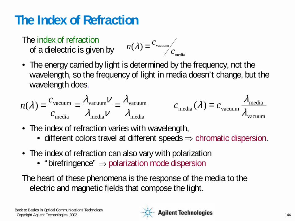
The Index of RefractionThe index of refraction
of a dielectric is given by• The energy carried by light is determined by the frequency, not the
wavelength, so the frequency of light in media doesn’t change, but the wavelength does.
• The index of refraction varies with wavelength,• different colors travel at different speeds ⇒ chromatic dispersion.
• The index of refraction can also vary with polarization• “birefringence” ⇒ polarization mode dispersion
The heart of these phenomena is the response of the media to theelectric and magnetic fields that compose the light.
media
vacuum)( ccn =λ
media
vacuum
media
vacuum
media
vacuum)(λλ
νλνλλ ===
ccn
vacuum
mediavacuummedia )(
λλλ cc =
Back to Basics in Optical Communications TechnologyCopyright Agilent Technologies, 2002 145
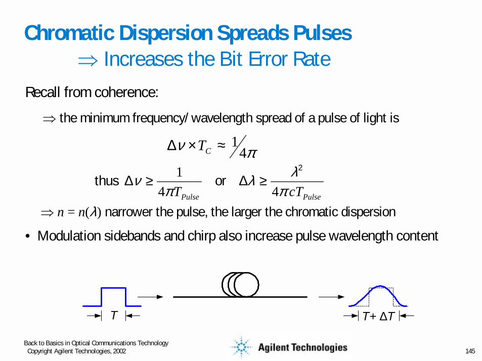
Chromatic Dispersion Spreads Pulses⇒ Increases the Bit Error Rate
Recall from coherence:⇒ the minimum frequency/wavelength spread of a pulse of light is
⇒ n = n(λ) narrower the pulse, the larger the chromatic dispersion
• Modulation sidebands and chirp also increase pulse wavelength content
πν 41≈×∆ CT
PulsePulse cTT πλλ
πν
441 2
or thus ≥∆≥∆
T T+ ∆T

Back to Basics in Optical Communications TechnologyCopyright Agilent Technologies, 2002 146
The Cause of Chromatic DispersionTwo causes:
1. Material Dispersion• The response, “permittivity”, of the media:
2. Waveguide Dispersion• ncore(λ) and ncladding(λ) vary differently with λ⇒ different boundary conditions for different wavelengths⇒ different solutions to the wave equation
x
κεε
µεεµλ =≈==
000media
vacuum)(ccn
Dielectric constant
Back to Basics in Optical Communications TechnologyCopyright Agilent Technologies, 2002 147
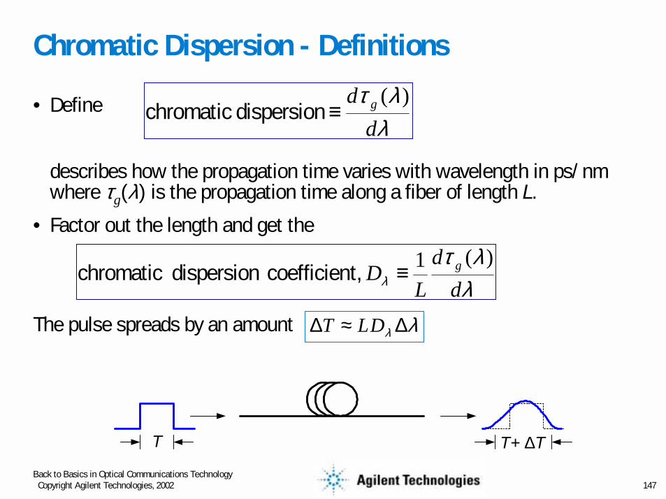
Chromatic Dispersion - Definitions
• Define
describes how the propagation time varies with wavelength in ps/nm where τg(λ) is the propagation time along a fiber of length L.
• Factor out the length and get the
The pulse spreads by an amount
λλτ
dd g )(
≡dispersionchromatic
λλτ
λ dd
LD g )(1≡ t,coefficien dispersion chromatic
λλ ∆≈∆ DLT
T T+ ∆T
Back to Basics in Optical Communications TechnologyCopyright Agilent Technologies, 2002 148
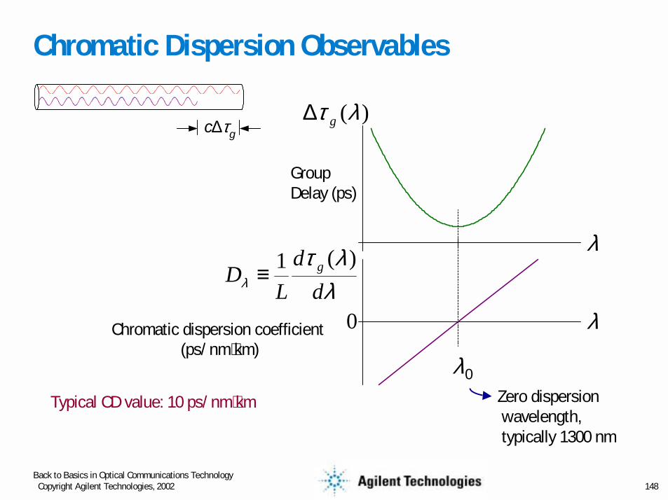
Chromatic Dispersion Observables
)(λτ g∆
GroupDelay (ps)
λ
λ
λ0
Chromatic dispersion coefficient (ps/nm⋅km)
λλτ
λ dd
LD g )(1≡
Zero dispersionwavelength, typically 1300 nm
c∆τg
0
Typical CD value: 10 ps/nm⋅km
Back to Basics in Optical Communications TechnologyCopyright Agilent Technologies, 2002 149
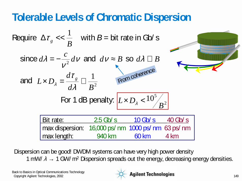
Tolerable Levels of Chromatic Dispersion
Require with B = bit rate in Gb/s
since and so
and
For 1 dB penalty:
Bg1<<∆τ
νν
λ dcd 2−= Bd ≈ν
21
Bdd
DL g ∝=×λτ
λ
Bd ∝λ
2510
BDL <× λ
Bit rate: 2.5 Gb/s 10 Gb/s 40 Gb/smax dispersion: 16,000 ps/nm 1000 ps/nm 63 ps/nmmax length: 940 km 60 km 4 km
Dispersion can be good! DWDM systems can have very high power density 1 mW/λ → 1 GW/m2 Dispersion spreads out the energy, decreasing energy densities.
From coherence
Back to Basics in Optical Communications TechnologyCopyright Agilent Technologies, 2002 150
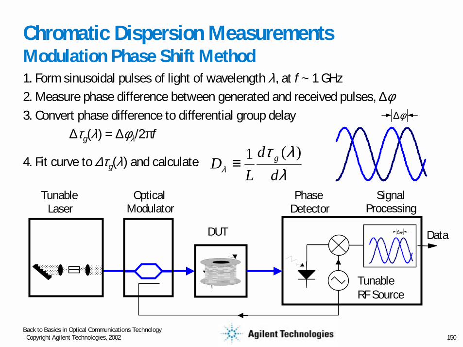
Chromatic Dispersion MeasurementsModulation Phase Shift Method
OpticalModulator
DUT
TunableLaser
TunableRF Source
PhaseDetector
SignalProcessing
Data
1. Form sinusoidal pulses of light of wavelength λ, at f ~ 1 GHz2. Measure phase difference between generated and received pulses, ∆φ3. Convert phase difference to differential group delay
∆τg(λ) = ∆φλ/2πf
4. Fit curve to ∆τg(λ) and calculate λλτ
λ dd
LD g )(1≡
∆φ
∆φ
Back to Basics in Optical Communications TechnologyCopyright Agilent Technologies, 2002 151
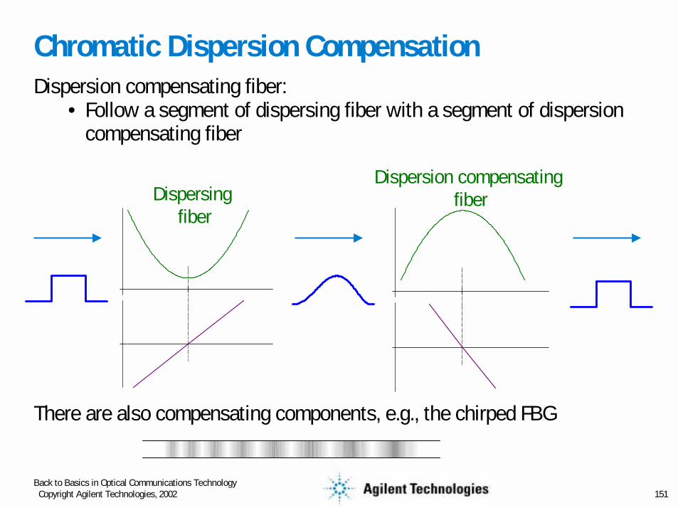
Chromatic Dispersion CompensationDispersion compensating fiber:
• Follow a segment of dispersing fiber with a segment of dispersion compensating fiber
There are also compensating components, e.g., the chirped FBG
Dispersing fiber
Dispersion compensating fiber
Back to Basics in Optical Communications TechnologyCopyright Agilent Technologies, 2002 152
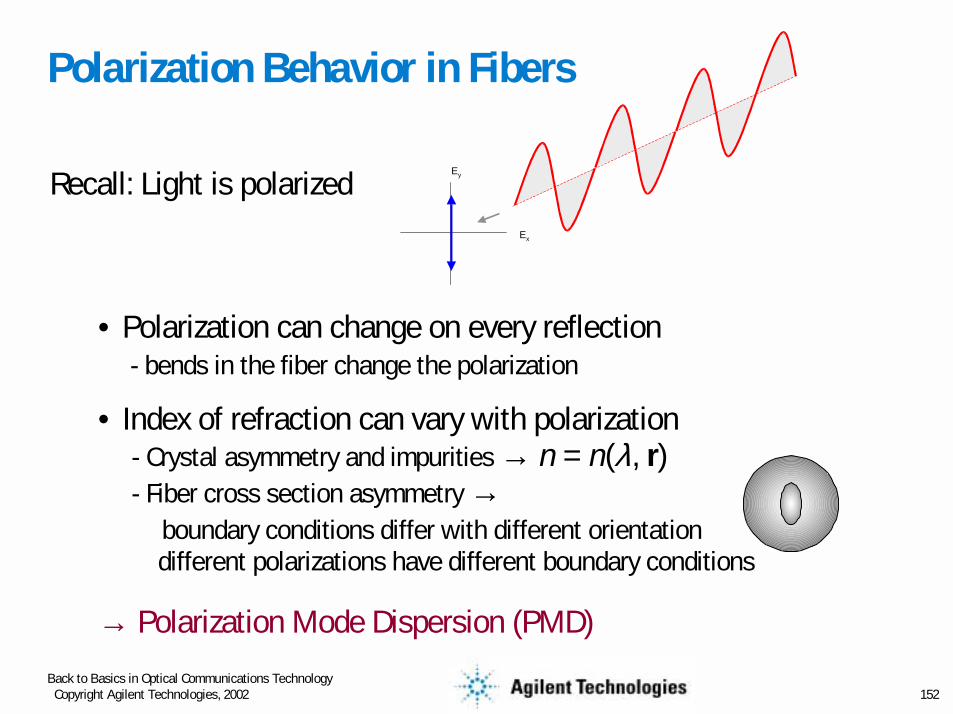
Polarization Behavior in Fibers
Recall: Light is polarized
• Polarization can change on every reflection- bends in the fiber change the polarization
• Index of refraction can vary with polarization- Crystal asymmetry and impurities → n = n(λ, r)- Fiber cross section asymmetry →
boundary conditions differ with different orientation different polarizations have different boundary conditions
→ Polarization Mode Dispersion (PMD)
Ey
Ex
Back to Basics in Optical Communications TechnologyCopyright Agilent Technologies, 2002 153
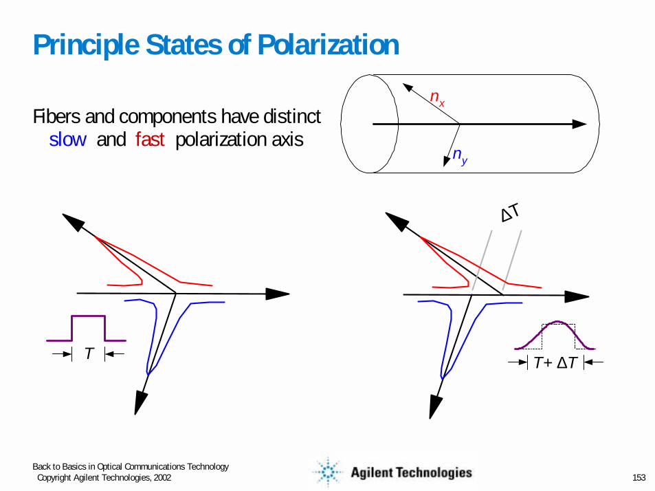
Principle States of Polarization
Fibers and components have distinctslow and fast polarization axis
T T+ ∆T
∆Τ
nx
ny
Back to Basics in Optical Communications TechnologyCopyright Agilent Technologies, 2002 154
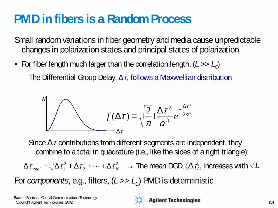
PMD in fibers is a Random ProcessSmall random variations in fiber geometry and media cause unpredictable
changes in polarization states and principal states of polarization• For fiber length much larger than the correlation length, (L >> LC)
The Differential Group Delay, ∆τ, follows a Maxwellian distribution
Since ∆τ contributions from different segments are independent, they combine to a total in quadrature (i.e., like the sides of a right triangle):
→ The mean DGD, ⟨∆τ⟩, increases with
For components, e.g., filters, (L >> LC) PMD is deterministic
2
2
23
22)( ατ
ατ
πτ
∆−∆⋅=∆ ef
222
21 Ntotal ττττ ∆++∆+∆=∆ L L
∆τ
N
Back to Basics in Optical Communications TechnologyCopyright Agilent Technologies, 2002 155
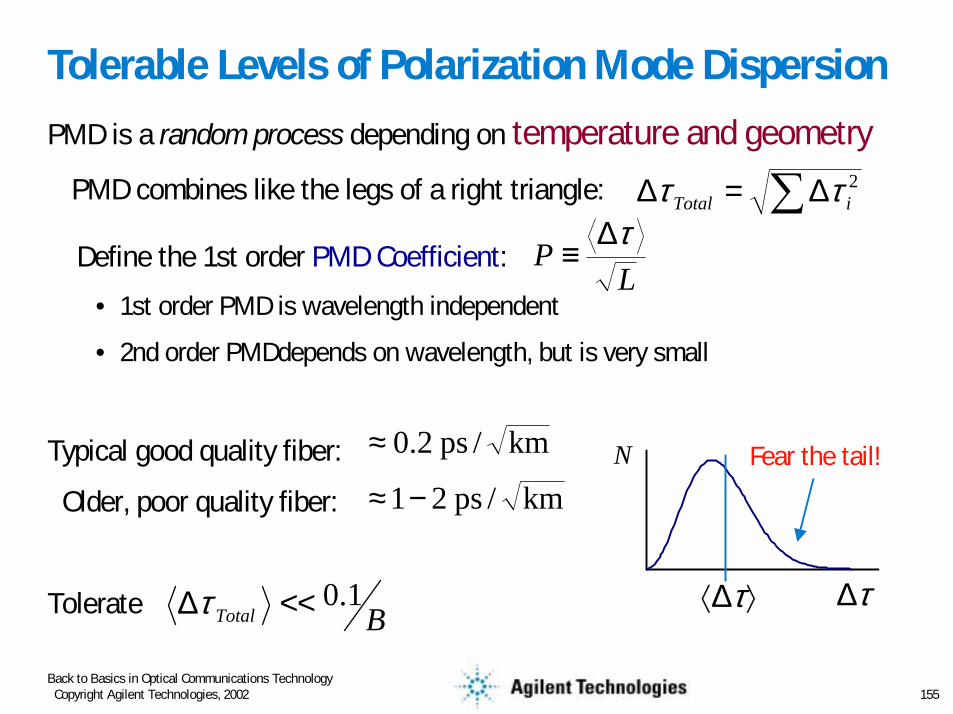
Tolerable Levels of Polarization Mode DispersionPMD is a random process depending on temperature and geometry
PMD combines like the legs of a right triangle:
Define the 1st order PMD Coefficient:• 1st order PMD is wavelength independent• 2nd order PMDdepends on wavelength, but is very small
Typical good quality fiber:Older, poor quality fiber:
Tolerate
LP
τ∆≡
∑∆=∆ 2iTotal ττ
km/ps2.0≈
km/ps21−≈
BTotal1.0<<∆τ ∆τ
N
⟨∆τ⟩
Fear the tail!
Back to Basics in Optical Communications TechnologyCopyright Agilent Technologies, 2002 156
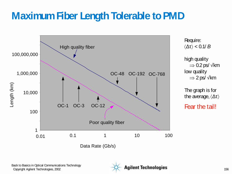
Maximum Fiber Length Tolerable to PMD
Require: ⟨∆τ⟩ < 0.1/B
high quality ⇒ 0.2 ps/√km
low quality ⇒ 2 ps/√km
The graph is for the average, ⟨∆τ⟩
Fear the tail!
1
100
10,000
1,000,000
100,000,000
Leng
th ( k
m)
Data Rate (Gb/s)
0.01 0.1 1 10 100
OC-1 OC-3 OC-12
OC-48 OC-192 OC-768
High quality fiber
Poor quality fiber
Back to Basics in Optical Communications TechnologyCopyright Agilent Technologies, 2002 157
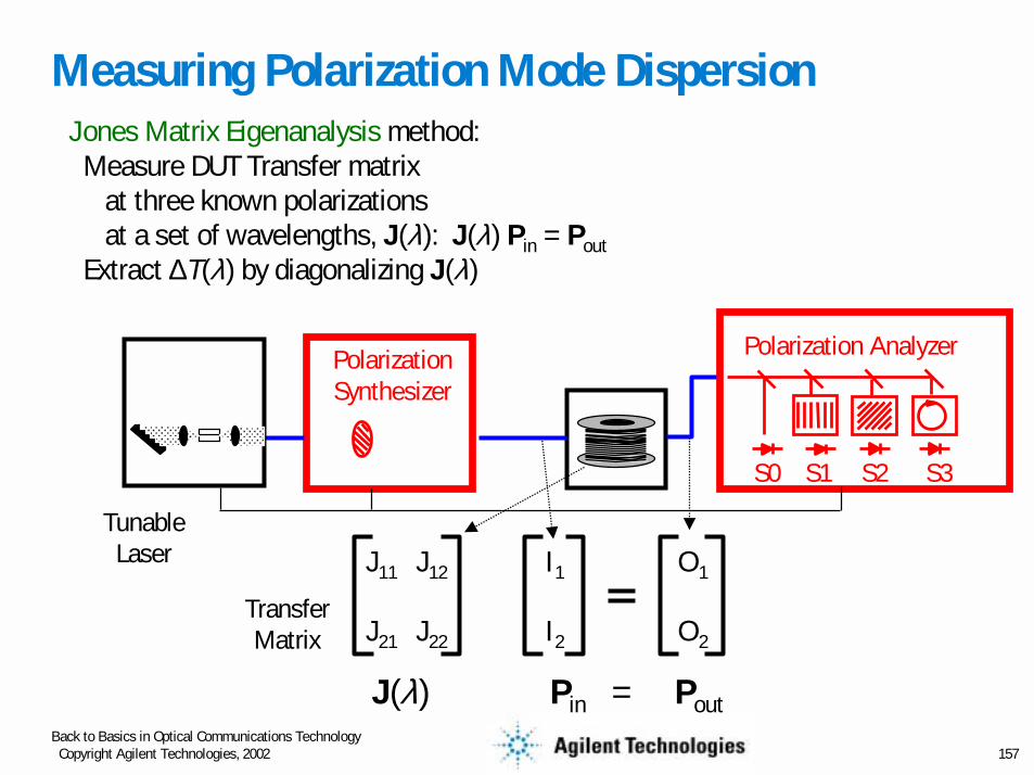
Measuring Polarization Mode DispersionJones Matrix Eigenanalysis method:
Measure DUT Transfer matrix at three known polarizations at a set of wavelengths, J(λ): J(λ) Pin = Pout
Extract ∆T(λ) by diagonalizing J(λ)
PolarizationSynthesizer
Polarization Analyzer
S0 S1 S2 S3
TunableLaser
TransferMatrix
O1
O2
I1
I2
J11 J12
J21 J22
J(λ) Pin = Pout
Back to Basics in Optical Communications TechnologyCopyright Agilent Technologies, 2002 158
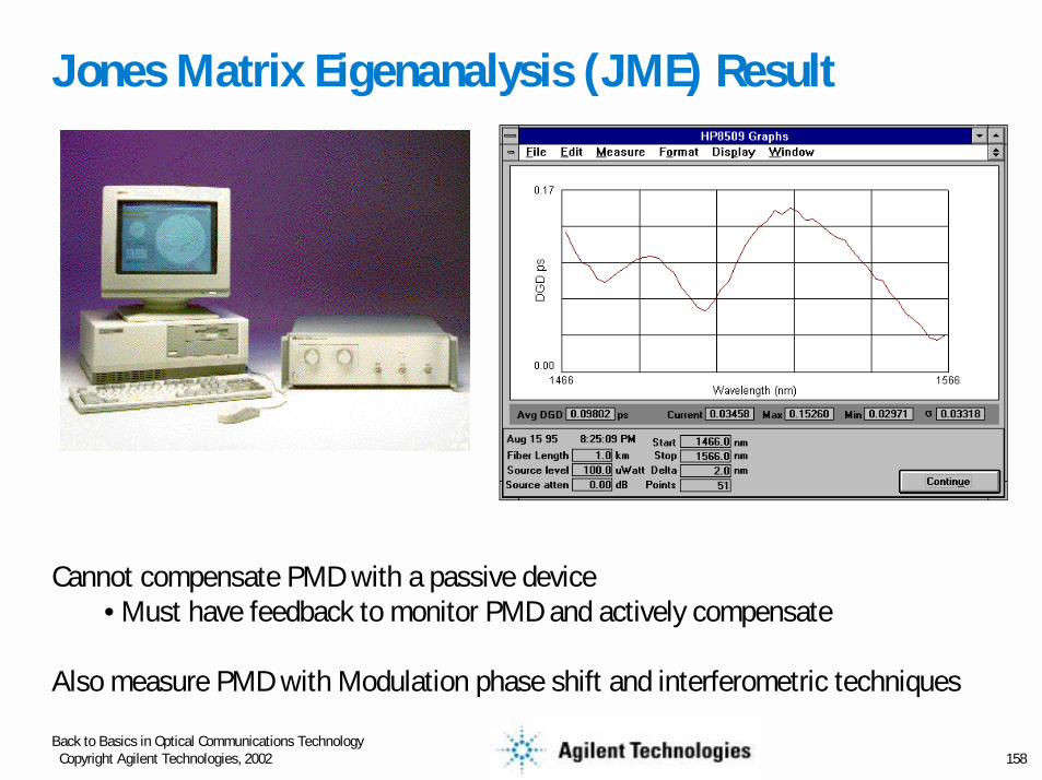
Jones Matrix Eigenanalysis (JME) Result
Cannot compensate PMD with a passive device• Must have feedback to monitor PMD and actively compensate
Also measure PMD with Modulation phase shift and interferometric techniques
Back to Basics in Optical Communications TechnologyCopyright Agilent Technologies, 2002 159
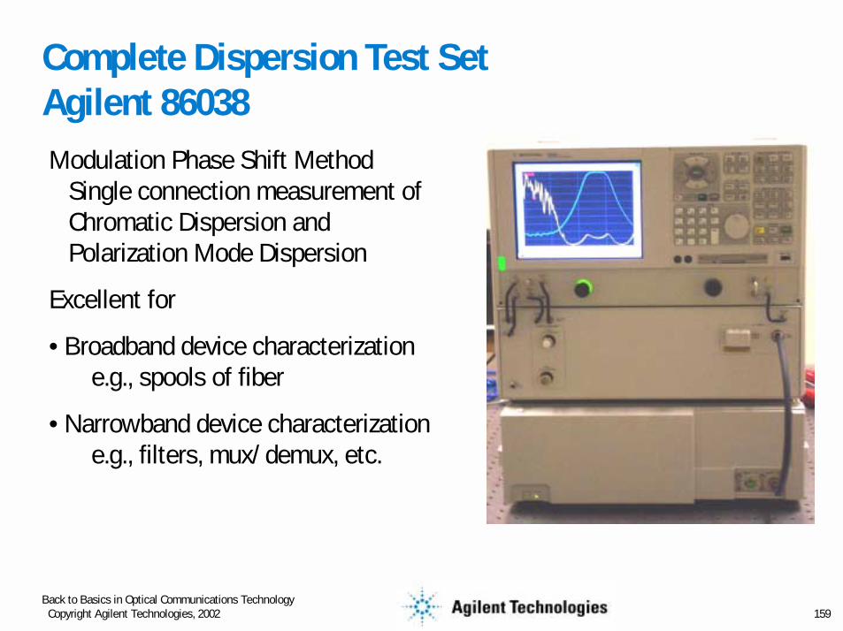
Complete Dispersion Test SetAgilent 86038Modulation Phase Shift Method
Single connection measurement of Chromatic Dispersion and Polarization Mode Dispersion
Excellent for
• Broadband device characterizatione.g., spools of fiber
• Narrowband device characterizatione.g., filters, mux/demux, etc.

Back to Basics in Optical Communications TechnologyCopyright Agilent Technologies, 2002 160
All Parameter Test SetAgilent 81910
Part of the Agilent Lightwave Measurement System (816x)• Swept insertion loss, return loss, polarization dependent loss• Chromatic and Polarization Mode Dispersion - interferometric technique
both insertion and reflection
Optimized for narrow-band components (e.g., filters, mux/demux, isolators, etc.)
Back to Basics in Optical Communications TechnologyCopyright Agilent Technologies, 2002 161
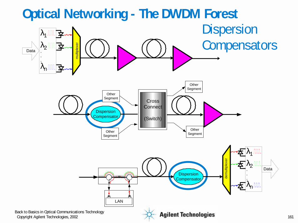
Optical Networking - The DWDM ForestDispersion Compensators
DispersionCompensator
DispersionCompensator
OtherSegment
OtherSegment
OtherSegment
OtherSegment
LAN
CrossConnect
(Switch)
Data
λ1
λ2...λn
Data
λ1
λ2...λn
dem
ultip
lexe
r
mul
tiple
xer
Back to Basics in Optical Communications TechnologyCopyright Agilent Technologies, 2002 162
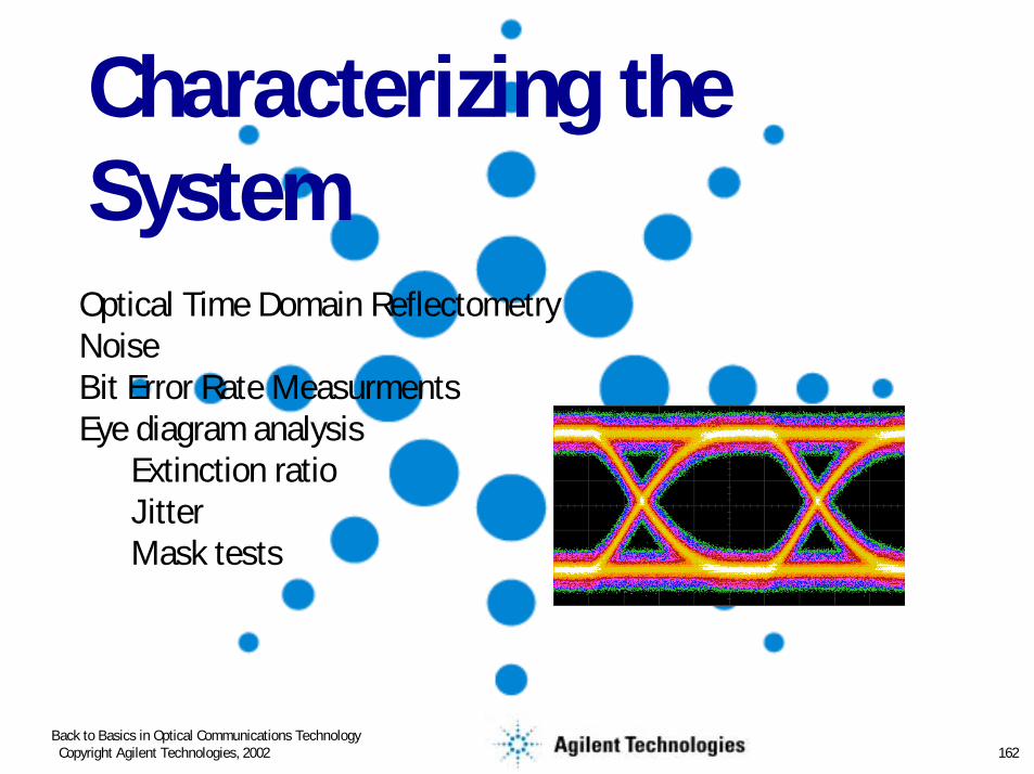
Characterizing the System
Optical Time Domain ReflectometryNoiseBit Error Rate MeasurmentsEye diagram analysis
Extinction ratioJitterMask tests
Back to Basics in Optical Communications TechnologyCopyright Agilent Technologies, 2002 163
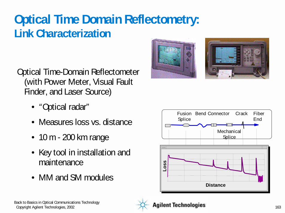
Optical Time Domain Reflectometry:Link Characterization
Optical Time-Domain Reflectometer (with Power Meter, Visual Fault Finder, and Laser Source)
• “Optical radar”• Measures loss vs. distance• 10 m - 200 km range• Key tool in installation and
maintenance• MM and SM modules
FusionSplice
Bend Connector Crack FiberEnd
MechanicalSplice
Loss
Distance
Back to Basics in Optical Communications TechnologyCopyright Agilent Technologies, 2002 164
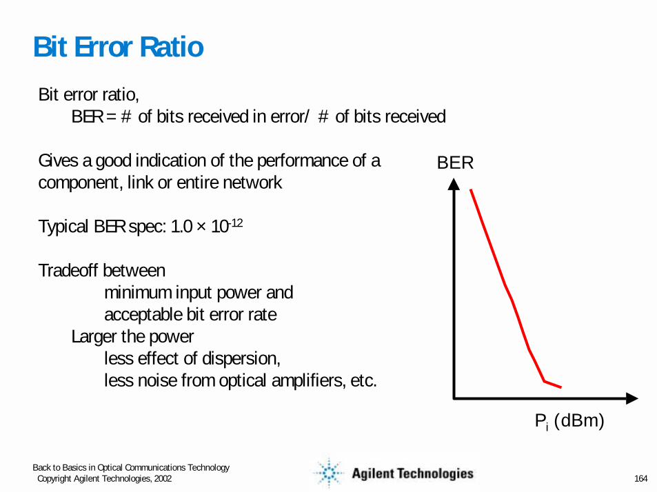
Bit Error RatioBit error ratio,
BER = # of bits received in error/ # of bits received
Gives a good indication of the performance of a component, link or entire network
Typical BER spec: 1.0 × 10⁻¹²
Tradeoff between minimum input power and acceptable bit error rate
Larger the power less effect of dispersion, less noise from optical amplifiers, etc.
Pi (dBm)
BER
Back to Basics in Optical Communications TechnologyCopyright Agilent Technologies, 2002 165
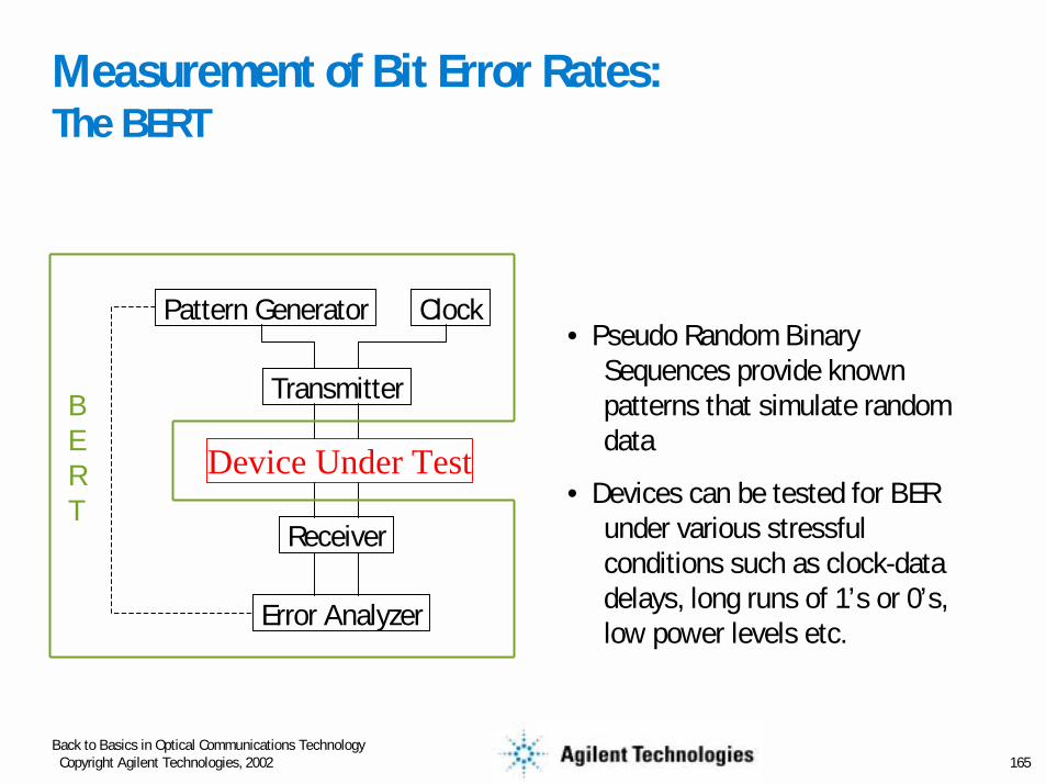
Measurement of Bit Error Rates:The BERT
Pattern Generator
Transmitter
Receiver
Error Analyzer
Clock
Device Under Test
• Pseudo Random BinarySequences provide knownpatterns that simulate randomdata
• Devices can be tested for BERunder various stressfulconditions such as clock-datadelays, long runs of 1’s or 0’s,low power levels etc.
BERT
Back to Basics in Optical Communications TechnologyCopyright Agilent Technologies, 2002 166
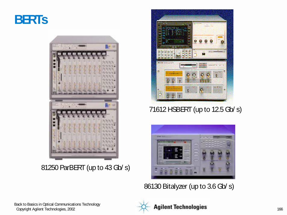
BERTs
86130 Bitalyzer (up to 3.6 Gb/s)
71612 HSBERT (up to 12.5 Gb/s)
81250 ParBERT (up to 43 Gb/s)
Back to Basics in Optical Communications TechnologyCopyright Agilent Technologies, 2002 167
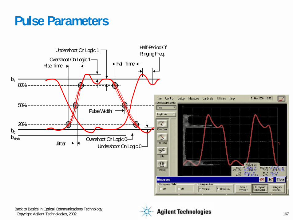
Pulse Parameters
Overshoot On Logic 1
b180%
50%
20%b0
b dark
Fall Time
Half-Period OfRinging Freq.
Pulse Width
Overshoot On Logic 0Undershoot On Logic 0
Undershoot On Logic 1
Rise Time
Jitter
Back to Basics in Optical Communications TechnologyCopyright Agilent Technologies, 2002 168
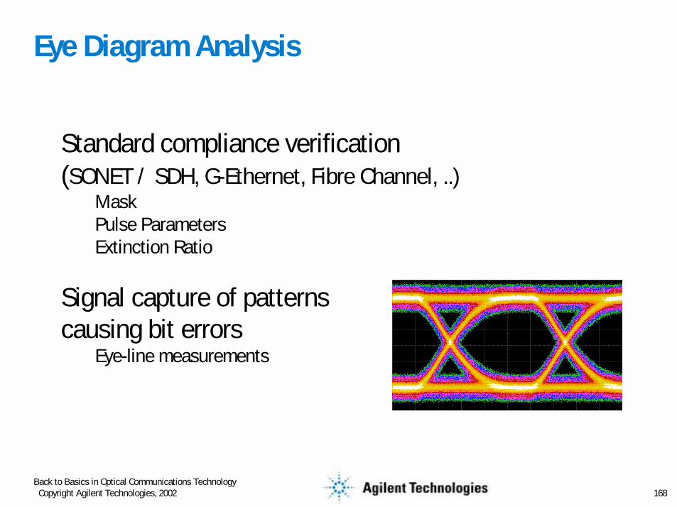
Eye Diagram Analysis
Standard compliance verification(SONET / SDH, G-Ethernet, Fibre Channel, ..)
MaskPulse ParametersExtinction Ratio
Signal capture of patterns causing bit errors
Eye-line measurements
Back to Basics in Optical Communications TechnologyCopyright Agilent Technologies, 2002 169
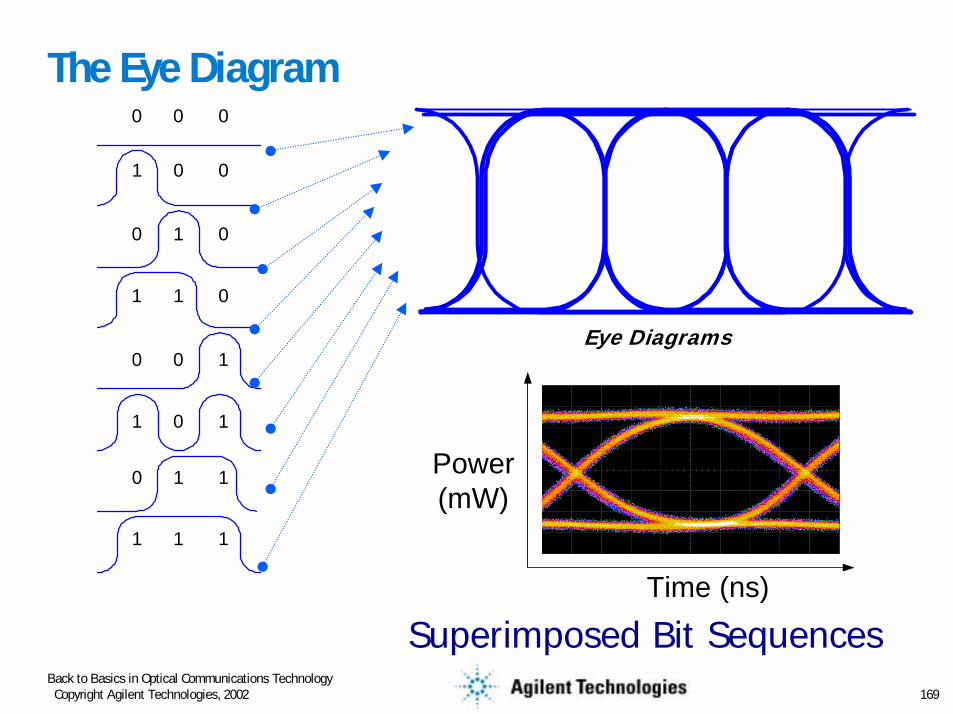
1 0 0
0 0 1
0 1 0
0 1 1
0 0 0
1 0 1
1 1 0
1 1 1
Superimposed Bit Sequences
Eye Diagrams
The Eye Diagram
Power(mW)
Time (ns)
Back to Basics in Optical Communications TechnologyCopyright Agilent Technologies, 2002 170
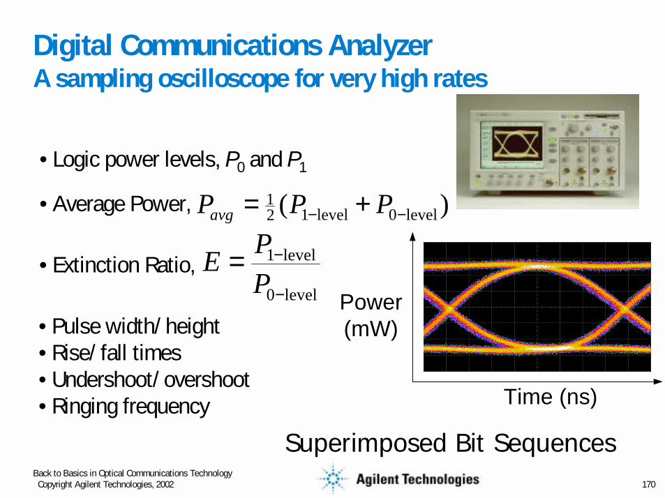
Digital Communications AnalyzerA sampling oscilloscope for very high rates
Superimposed Bit Sequences
• Extinction Ratio,level0
level1
−
−=PPE
• Logic power levels, P0 and P1
• Average Power, )( level0level121
−− += PPPavg
Power(mW)
Time (ns)
• Pulse width/height • Rise/fall times• Undershoot/overshoot• Ringing frequency
Back to Basics in Optical Communications TechnologyCopyright Agilent Technologies, 2002 171
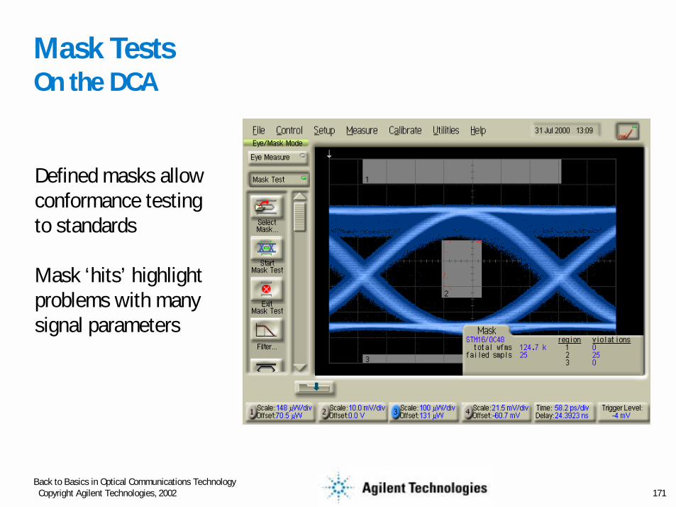
Mask TestsOn the DCA
Defined masks allow conformance testing to standards
Mask ‘hits’ highlight problems with many signal parameters
Back to Basics in Optical Communications TechnologyCopyright Agilent Technologies, 2002 172
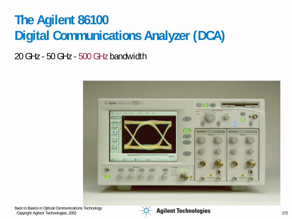
The Agilent 86100 Digital Communications Analyzer (DCA)20 GHz - 50 GHz - 500 GHz bandwidth
Back to Basics in Optical Communications TechnologyCopyright Agilent Technologies, 2002 173
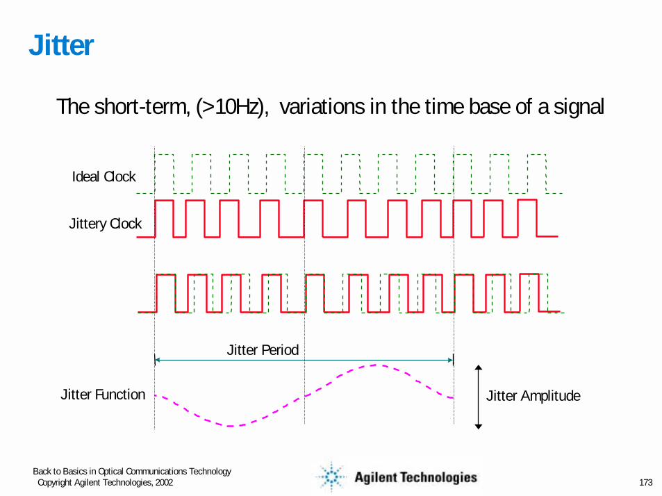
Jitter
The short-term, (>10Hz), variations in the time base of a signal
Jitter Period
Ideal Clock
Jittery Clock
Jitter Function Jitter Amplitude
Back to Basics in Optical Communications TechnologyCopyright Agilent Technologies, 2002 174
Characterizing Jitter
Jitter can be measured either as RMS variations or peak-peak• Jitter Tolerance = Amplitude of applied sinusoidal jitter to the
device under test resulting in a certain Bit Error Rate• Jitter Transfer = Ratio of the output jitter amplitude
to the amplitude of applied sinusoidal jitter• Jitter Generation/Intrinsic Jitter = Jitter produced by the device
under test
Random Jitter - sum of small random processes resulting in jitterDeterministic jitter - data dependent jitter, duty cycle distortion, etc
resulting in jitter
Back to Basics in Optical Communications TechnologyCopyright Agilent Technologies, 2002 175
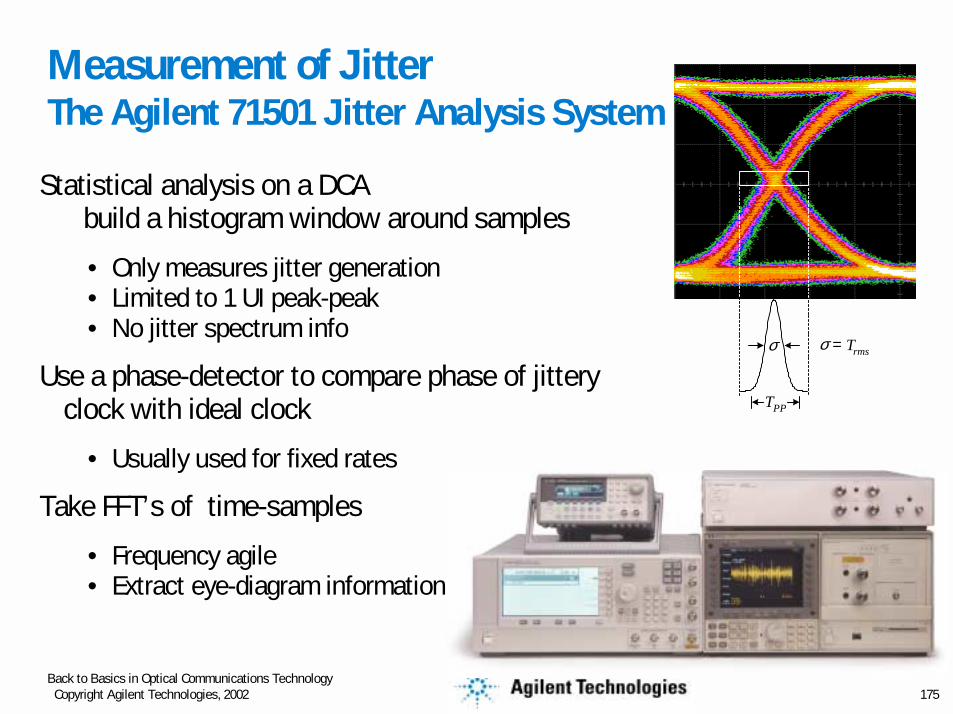
Measurement of JitterThe Agilent 71501 Jitter Analysis System
Statistical analysis on a DCA build a histogram window around samples• Only measures jitter generation• Limited to 1 UI peak-peak• No jitter spectrum info
Use a phase-detector to compare phase of jittery clock with ideal clock
• Usually used for fixed rates
Take FFT’s of time-samples• Frequency agile• Extract eye-diagram information
TPP
σ Trmsσ =
Back to Basics in Optical Communications TechnologyCopyright Agilent Technologies, 2002 176
Optical Networking - The DWDM Forest
DispersionCompensator
DispersionCompensator
OtherSegment
OtherSegment
OtherSegment
OtherSegment
LAN
CrossConnect
(Switch)
Data
λ1
λ2...λn
Data
λ1
λ2...λn
dem
ultip
lexe
r
mul
tiple
xer
Back to Basics in Optical Communications TechnologyCopyright Agilent Technologies, 2002 177
ConclusionA wealth of technologies have been developed for high speed
networking based on a few simple physical phenomena:• Reflection and refraction (geometric optics) ⇒
Optic fibers• Interference ⇒ Optical Spectrum Analysis
high resolution distance measurementsFilters, mux/demux, isolators, et ceteraexternal modulators
• Atomic transitions and Raman scattering ⇒LEDs, LASERsLight detectors - PIN diodes, APDsOptical Amplifiers
• Index of Refraction ⇒Chromatic and Polarization Mode Dispersion
Agilent develops technology that makes dreams real!
Back to Basics in Optical Communications TechnologyCopyright Agilent Technologies, 2002 178
ssss Agilent Technologies’ Lightwave Training and Services
Understanding Optical NetworkingUnderstanding Lightwave TechnologyUnderstanding DWDMUnderstanding Optical Passive Device
CharacterizationUnderstanding Optical Transmitters and
Receivers and Their Characterization
• TrainingFast Food Technician → Optical Engineering Nobel Laureate
Optical Spectrum Analysis/OSA User’s Course
Characterizing Polarization EffectsEye Diagram AnalysisTDR in High-Speed Digital DesignBit Error Rate AnalysisDigital Communications Analyzer User’s
Course
Design-to-Fit Training• Consulting and CustomizingTest and Measurement AutomationBrilliant and talented Applications Engineers and Scientists at your every whim. . .


![Optical Communications [OC]](https://static.fdocuments.net/doc/165x107/577d1fe11a28ab4e1e918737/optical-communications-oc.jpg)


![mb hnizmkhoc³ s{]m^. Fw.ssh. tbml¶m³ - Malayalam.pdf · Imte_v: [oc\mb hnizmkhoc³ s{]m^. Fw.ssh. tbml¶m³ dn«tbUv {]n³kn¸Â, skâv ]otägvkv tImtfPv, tImet©cn ta¨¦c, ISbncp¸v](https://static.fdocuments.net/doc/165x107/5f9d9b799c49e604734f83da/mb-hnizmkhoc-sm-fwssh-tbmlm-malayalampdf-imtev-ocmb-hnizmkhoc.jpg)
![[Presentation (pdf, 4.2 Mb)] - Harvard Universityacmg.seas.harvard.edu/presentations/IGC6/talks/MonD_BC_curci... · SENSITIVITY TESTS WITH GEOS-Chem AEROSOL OPTICAL PROPERTIES: THE](https://static.fdocuments.net/doc/165x107/5a9d74e07f8b9abd058d5ffa/presentation-pdf-42-mb-harvard-tests-with-geos-chem-aerosol-optical-properties.jpg)