AVR - Farnell element14 · non-intrusive real-time trace and full-speed read/write memory access,...
96
Features • High-performance, Low-power 32-bit Atmel ® AVR ® Microcontroller – Compact Single-cycle RISC Instruction Set Including DSP Instructions – Read-modify-write Instructions and Atomic Bit Manipulation – Performance • Up to 64DMIPS Running at 50MHz from Flash (1 Flash Wait State) • Up to 36DMIPS Running at 25MHz from Flash (0 Flash Wait State) – Memory Protection Unit (MPU) • Secure Access Unit (SAU) providing User-defined Peripheral Protection • picoPower ® Technology for Ultra-low Power Consumption • Multi-hierarchy Bus System – High-performance Data Transfers on Separate Buses for Increased Performance – 12 Peripheral DMA Channels Improve Speed for Peripheral Communication • Internal High-speed Flash – 256Kbytes and 128Kbytes Versions – Single-cycle Access up to 25MHz – FlashVault Technology Allows Pre-programmed Secure Library Support for End User Applications – Prefetch Buffer Optimizing Instruction Execution at Maximum Speed – 100,000 Write Cycles, 15-year Data Retention Capability – Flash Security Locks and User-defined Configuration Area • Internal High-speed SRAM, Single-cycle Access at Full Speed – 32Kbytes • Interrupt Controller (INTC) – Autovectored Low-latency Interrupt Service with Programmable Priority • External Interrupt Controller (EIC) • Peripheral Event System for Direct Peripheral to Peripheral Communication • System Functions – Power and Clock Manager – SleepWalking Power Saving Control – Internal System RC Oscillator (RCSYS) – 32 KHz Oscillator – Multipurpose Oscillator, Phase Locked Loop (PLL), and Digital Frequency Locked Loop (DFLL) • Windowed Watchdog Timer (WDT) • Asynchronous Timer (AST) with Real-time Clock Capability – Counter or Calendar Mode Supported • Frequency Meter (FREQM) for Accurate Measuring of Clock Frequency • Six 16-bit Timer/Counter (TC) Channels – External Clock Inputs, PWM, Capture, and Various Counting Capabilities • PWM Channels on All I/O Pins (PWMA) – 8-bit PWM with a Source Clock up to 150MHz • Four Universal Synchronous/Asynchronous Receiver/Transmitters (USART) – Independent Baudrate Generator, Support for SPI – Support for Hardware Handshaking • One Master/Slave Serial Peripheral Interface (SPI) with Chip Select Signals – Up to 15 SPI Slaves can be Addressed 32145BS–01/2012 32-bit Atmel AVR Microcontroller AT32UC3L0256 AT32UC3L0128 Summary
Transcript of AVR - Farnell element14 · non-intrusive real-time trace and full-speed read/write memory access,...

Features• High-performance, Low-power 32-bit Atmel® AVR® Microcontroller
– Compact Single-cycle RISC Instruction Set Including DSP Instructions– Read-modify-write Instructions and Atomic Bit Manipulation– Performance
• Up to 64DMIPS Running at 50MHz from Flash (1 Flash Wait State)• Up to 36DMIPS Running at 25MHz from Flash (0 Flash Wait State)
– Memory Protection Unit (MPU)• Secure Access Unit (SAU) providing User-defined Peripheral Protection
• picoPower® Technology for Ultra-low Power Consumption• Multi-hierarchy Bus System
– High-performance Data Transfers on Separate Buses for Increased Performance– 12 Peripheral DMA Channels Improve Speed for Peripheral Communication
• Internal High-speed Flash– 256Kbytes and 128Kbytes Versions– Single-cycle Access up to 25MHz– FlashVault Technology Allows Pre-programmed Secure Library Support for End
User Applications– Prefetch Buffer Optimizing Instruction Execution at Maximum Speed– 100,000 Write Cycles, 15-year Data Retention Capability– Flash Security Locks and User-defined Configuration Area
• Internal High-speed SRAM, Single-cycle Access at Full Speed– 32Kbytes
• Interrupt Controller (INTC)– Autovectored Low-latency Interrupt Service with Programmable Priority
• External Interrupt Controller (EIC)• Peripheral Event System for Direct Peripheral to Peripheral Communication• System Functions
– Power and Clock Manager – SleepWalking Power Saving Control– Internal System RC Oscillator (RCSYS)– 32 KHz Oscillator– Multipurpose Oscillator, Phase Locked Loop (PLL), and Digital Frequency Locked
Loop (DFLL)• Windowed Watchdog Timer (WDT)• Asynchronous Timer (AST) with Real-time Clock Capability
– Counter or Calendar Mode Supported• Frequency Meter (FREQM) for Accurate Measuring of Clock Frequency• Six 16-bit Timer/Counter (TC) Channels
– External Clock Inputs, PWM, Capture, and Various Counting Capabilities• PWM Channels on All I/O Pins (PWMA)
– 8-bit PWM with a Source Clock up to 150MHz• Four Universal Synchronous/Asynchronous Receiver/Transmitters (USART)
– Independent Baudrate Generator, Support for SPI– Support for Hardware Handshaking
• One Master/Slave Serial Peripheral Interface (SPI) with Chip Select Signals– Up to 15 SPI Slaves can be Addressed
32145BS–01/2012
32-bit Atmel AVR Microcontroller
AT32UC3L0256AT32UC3L0128
Summary

232145BS–01/2012
AT32UC3L0128/256
• Two Master and Two Slave Two-wire Interfaces (TWI), 400kbit/s I2C-compatible• One 8-channel Analog-to-digital Converter (ADC) with up to 12 Bits Resolution
– Internal Temperature Sensor• Eight Analog Comparators (AC) with Optional Window Detection• Capacitive Touch (CAT) Module
– Hardware-assisted Atmel® AVR® QTouch® and Atmel® AVR® QMatrix Touch Acquisition– Supports QTouch and QMatrix Capture from Capacitive Touch Sensors
• QTouch Library Support– Capacitive Touch Buttons, Sliders, and Wheels– QTouch and QMatrix Acquisition
• On-chip Non-intrusive Debug System– Nexus Class 2+, Runtime Control, Non-intrusive Data and Program Trace– aWire Single-pin Programming Trace and Debug Interface Muxed with Reset Pin– NanoTrace Provides Trace Capabilities through JTAG or aWire Interface
• 48-pin TQFP/QFN/TLLGA (36 GPIO Pins)• Five High-drive I/O Pins• Single 1.62-3.6 V Power Supply

332145BS–01/2012
AT32UC3L0128/256
1. DescriptionThe Atmel® AVR® AT32UC3L0128/256 is a complete system-on-chip microcontroller based onthe AVR32 UC RISC processor running at frequencies up to 50MHz. AVR32 UC is a high-per-formance 32-bit RISC microprocessor core, designed for cost-sensitive embedded applications,with particular emphasis on low power consumption, high code density, and high performance.
The processor implements a Memory Protection Unit (MPU) and a fast and flexible interrupt con-troller for supporting modern and real-time operating systems. The Secure Access Unit (SAU) isused together with the MPU to provide the required security and integrity.
Higher computation capability is achieved using a rich set of DSP instructions.
The AT32UC3L0128/256 embeds state-of-the-art picoPower technology for ultra-low power con-sumption. Combined power control techniques are used to bring active current consumptiondown to 174µA/MHz, and leakage down to 220nA while still retaining a bank of backup regis-ters. The device allows a wide range of trade-offs between functionality and power consumption,giving the user the ability to reach the lowest possible power consumption with the feature setrequired for the application.
The Peripheral Direct Memory Access (DMA) controller enables data transfers between periph-erals and memories without processor involvement. The Peripheral DMA controller drasticallyreduces processing overhead when transferring continuous and large data streams.
The AT32UC3L0128/256 incorporates on-chip Flash and SRAM memories for secure and fastaccess. The FlashVault technology allows secure libraries to be programmed into the device.The secure libraries can be executed while the CPU is in Secure State, but not read by non-secure software in the device. The device can thus be shipped to end customers, who will beable to program their own code into the device to access the secure libraries, but without risk ofcompromising the proprietary secure code.
The External Interrupt Controller (EIC) allows pins to be configured as external interrupts. Eachexternal interrupt has its own interrupt request and can be individually masked.
The Peripheral Event System allows peripherals to receive, react to, and send peripheral eventswithout CPU intervention. Asynchronous interrupts allow advanced peripheral operation in lowpower sleep modes.
The Power Manager (PM) improves design flexibility and security. The Power Manager supportsSleepWalking functionality, by which a module can be selectively activated based on peripheralevents, even in sleep modes where the module clock is stopped. Power monitoring is supportedby on-chip Power-on Reset (POR), Brown-out Detector (BOD), and Supply Monitor (SM). Thedevice features several oscillators, such as Phase Locked Loop (PLL), Digital FrequencyLocked Loop (DFLL), Oscillator 0 (OSC0), and system RC oscillator (RCSYS). Either of theseoscillators can be used as source for the system clock. The DFLL is a programmable internaloscillator from 20 to 150MHz. It can be tuned to a high accuracy if an accurate reference clock isrunning, e.g. the 32KHz crystal oscillator.
The Watchdog Timer (WDT) will reset the device unless it is periodically serviced by the soft-ware. This allows the device to recover from a condition that has caused the system to beunstable.
The Asynchronous Timer (AST) combined with the 32KHz crystal oscillator supports powerfulreal-time clock capabilities, with a maximum timeout of up to 136 years. The AST can operate incounter mode or calendar mode.

432145BS–01/2012
AT32UC3L0128/256
The Frequency Meter (FREQM) allows accurate measuring of a clock frequency by comparing itto a known reference clock.
The device includes six identical 16-bit Timer/Counter (TC) channels. Each channel can be inde-pendently programmed to perform frequency measurement, event counting, intervalmeasurement, pulse generation, delay timing, and pulse width modulation.
The Pulse Width Modulation controller (PWMA) provides 8-bit PWM channels which can be syn-chronized and controlled from a common timer. One PWM channel is available for each I/O pinon the device, enabling applications that require multiple PWM outputs, such as LCD backlightcontrol. The PWM channels can operate independently, with duty cycles set individually, or ininterlinked mode, with multiple channels changed at the same time.
The AT32UC3L0128/256 also features many communication interfaces, like USART, SPI, andTWI, for communication intensive applications. The USART supports different communicationmodes, like SPI Mode and LIN Mode.
A general purpose 8-channel ADC is provided, as well as eight analog comparators (AC). TheADC can operate in 10-bit mode at full speed or in enhanced mode at reduced speed, offeringup to 12-bit resolution. The ADC also provides an internal temperature sensor input channel.The analog comparators can be paired to detect when the sensing voltage is within or outsidethe defined reference window.
The Capacitive Touch (CAT) module senses touch on external capacitive touch sensors, usingthe QTouch technology. Capacitive touch sensors use no external mechanical components,unlike normal push buttons, and therefore demand less maintenance in the user application.The CAT module allows up to 17 touch sensors, or up to 16 by 8 matrix sensors to be interfaced.All touch sensors can be configured to operate autonomously without software interaction,allowing wakeup from sleep modes when activated.
Atmel offers the QTouch library for embedding capacitive touch buttons, sliders, and wheelsfunctionality into AVR microcontrollers. The patented charge-transfer signal acquisition offersrobust sensing and includes fully debounced reporting of touch keys as well as Adjacent KeySuppression® (AKS®) technology for unambiguous detection of key events. The easy-to-useQTouch Suite toolchain allows you to explore, develop, and debug your own touch applications.
The AT32UC3L0128/256 integrates a class 2+ Nexus 2.0 On-chip Debug (OCD) System, withnon-intrusive real-time trace and full-speed read/write memory access, in addition to basic run-time control. The NanoTrace interface enables trace feature for aWire- or JTAG-baseddebuggers. The single-pin aWire interface allows all features available through the JTAG inter-face to be accessed through the RESET pin, allowing the JTAG pins to be used for GPIO orperipherals.

532145BS–01/2012
AT32UC3L0128/256
2. Overview
2.1 Block Diagram
Figure 2-1. Block Diagram
SYSTEM CONTROL INTERFACE
INTERRUPT CONTROLLER
ASYNCHRONOUS TIMER
PERIPHERALDMA
CONTROLLER
HSB-PB BRIDGE B
HSB-PB BRIDGE A
S
M M M
S
S
M
EXTERNAL INTERRUPTCONTROLLER
HIGH SPEEDBUS MATRIX
GE
NER
ALP
UR
PO
SE
I/O
s
GEN
ER
AL P
UR
POSE
I/O
s
PAPB
EXTINT[5..1]
NMI
GCLK[4..0]
PAPB
SPI
DM
A MISO, MOSI
NPCS[3..0]
USART0USART1USART2USART3
DM
A
RXDTXDCLK
RTS, CTS
WATCHDOGTIMER
SCK
JTAGINTERFACE
MCKOMDO[5..0]
MSEO[1..0]EVTI_N
TDOTDITMS
CONFIGURATION REGISTERS BUS
128/256 KBFLASHS FL
ASH
CO
NTR
OLL
ER
EVTO_N
AVR32UC CPUNEXUS
CLASS 2+OCD
INSTRINTERFACE
DATAINTERFACE M
EM
OR
Y IN
TER
FAC
E LOCAL BUS
32 KB SRAM
MEMORY PROTECTION UNIT
LOCAL BUSINTERFACE
FREQUENCY METER
PWM CONTROLLERPWMA[35..0]
TIMER/COUNTER 0TIMER/COUNTER 1
A[2..0]
B[2..0]
TWI MASTER 0TWI MASTER 1D
MA
TWI SLAVE 0TWI SLAVE 1D
MA
8-CHANNEL ADC INTERFACED
MA
AD[8..0]
ADVREFP
POWER MANAGER
RESETCONTROLLER
SLEEPCONTROLLER
CLOCKCONTROLLER
XIN32XOUT32 OSC32K
RCSYS
XIN0XOUT0 OSC0
DFLL
TCK
aWireRESET_N
CAPACITIVE TOUCHMODULED
MA
CSB[16:0]SMP
CSA[16:0]
SYNC
AC INTERFACEACREFN
ACAN[3..0]
ACBN[3..0]ACBP[3..0]
ACAP[3..0]
TWCK
TWD
TWALM
TWCK
TWD
TWALM
RC32K
RC120M
GLUE LOGIC CONTROLLER IN[7..0]
OUT[1:0]
DATAOUT
SAU S/M
VDIVENDIS
TRIGGERADP[1..0]
RC32OUT
PLL
GCLK_IN[1..0]
CLK[2..0]

632145BS–01/2012
AT32UC3L0128/256
2.2 Configuration Summary
Table 2-1. Configuration Summary
Feature AT32UC3L0256 AT32UC3L0128
Flash 256KB 128KB
SRAM 32KB
GPIO 36
High-drive pins 5
External Interrupts 6
TWI 2
USART 4
Peripheral DMA Channels 12
Peripheral Event System 1
SPI 1
Asynchronous Timers 1
Timer/Counter Channels 6
PWM channels 36
Frequency Meter 1
Watchdog Timer 1
Power Manager 1
Secure Access Unit 1
Glue Logic Controller 1
Oscillators
Digital Frequency Locked Loop 20-150 MHz (DFLL)
Phase Locked Loop 40-240 MHz (PLL)Crystal Oscillator 0.45-16 MHz (OSC0)
Crystal Oscillator 32 KHz (OSC32K)
RC Oscillator 120MHz (RC120M)RC Oscillator 115 kHz (RCSYS)
RC Oscillator 32 kHz (RC32K)
ADC 8-channel 12-bit
Temperature Sensor 1
Analog Comparators 8
Capacitive Touch Module 1
JTAG 1
aWire 1
Max Frequency 50 MHz
Packages TQFP48/QFN48/TLLGA48

732145BS–01/2012
AT32UC3L0128/256
3. Package and Pinout
3.1 PackageThe device pins are multiplexed with peripheral functions as described in Section 3.2.1.
Figure 3-1. TQFP48/QFN48 Pinout
GN
D1
PA
092
PA
083
PA
034
PB
125
PB
006
PB
027
PB
038
PA
229
PA
0610
PA
0011
PA
0512
PA0213PA0114PA0715PB0116VDDIN17VDDCORE18GND19PB0520PB0421RESET_N22PB1023PA2124
PA
1436
VD
DAN
A35
AD
VR
EFP
34G
ND
AN
A33
PB
0832
PB
0731
PB
0630
PB
0929
PA
0428
PA
1127
PA
1326
PA
2025
PA15 37PA16 38PA17 39PA19 40PA18 41
VDDIO 42GND 43PB11 44GND 45PA10 46PA12 47
VDDIO 48

832145BS–01/2012
AT32UC3L0128/256
Figure 3-2. TLLGA48 Pinout
3.2 Peripheral Multiplexing on I/O Lines
3.2.1 Multiplexed SignalsEach GPIO line can be assigned to one of the peripheral functions. The following tabledescribes the peripheral signals multiplexed to the GPIO lines.
GN
D1
PA
092
PA
083
PA
034
PB
125
PB
006
PB
027
PB
038
PA
229
PA
0610
PA
0011
PA
0512
PA
0213
PA0114PA0715PB0116VDDIN17VDDCORE18GND19PB0520PB0421RESET_N22PB1023PA2124
PA
1436
VD
DA
NA
35AD
VREF
P34
GN
DA
NA
33P
B08
32P
B07
31P
B06
30P
B09
29P
A04
28P
A11
27P
A13
26P
A20
25
PA
1537
PA16 38PA17 39PA19 40PA18 41
VDDIO 42GND 43PB11 44GND 45PA10 46PA12 47
VDDIO 48
Table 3-1. GPIO Controller Function Multiplexing
48-pin PIN
GP I O Supply
Pin Type
GPIO Function
A B C D E F G H
11 PA00 0 VDDIO Normal I/O
USART0 TXD
USART1 RTS
SPI NPCS[2]
PWMA PWMA[0]
SCIF GCLK[0]
CAT CSA[2]
14 PA01 1 VDDIO Normal I/O
USART0 RXD
USART1 CTS
SPI NPCS[3]
USART1 CLK
PWMA PWMA[1]
ACIFB ACAP[0]
TWIMS0 TWALM
CAT CSA[1]

932145BS–01/2012
AT32UC3L0128/256
13 PA02 2 VDDIO High-drive I/O
USART0 RTS
ADCIFB TRIGGER
USART2 TXD
TC0 A0
PWMA PWMA[2]
ACIFB ACBP[0]
USART0 CLK
CAT CSA[3]
4 PA03 3 VDDIO Normal I/O
USART0 CTS
SPI NPCS[1]
USART2 TXD
TC0 B0
PWMA PWMA[3]
ACIFB ACBN[3]
USART0 CLK
CAT CSB[3]
28 PA04 4 VDDIO Normal I/O
SPI MISO
TWIMS0 TWCK
USART1 RXD
TC0 B1
PWMA PWMA[4]
ACIFB ACBP[1]
CAT CSA[7]
12 PA05 5 VDDIO Normal I/O (TWI)
SPI MOSI
TWIMS1 TWCK
USART1 TXD
TC0 A1
PWMA PWMA[5]
ACIFB ACBN[0]
TWIMS0 TWD
CAT CSB[7]
10 PA06 6 VDDIO
High-drive I/O,
5V tolerant
SPI SCK
USART2 TXD
USART1 CLK
TC0 B0
PWMA PWMA[6]
EIC EXTINT[2]
SCIF GCLK[1]
CAT CSB[1]
15 PA07 7 VDDIO Normal I/O (TWI)
SPI NPCS[0]
USART2 RXD
TWIMS1 TWALM
TWIMS0 TWCK
PWMA PWMA[7]
ACIFB ACAN[0]
EIC NMI
(EXTINT[0])
CAT CSB[2]
3 PA08 8 VDDIO High-drive I/O
USART1 TXD
SPI NPCS[2]
TC0 A2
ADCIFB ADP[0]
PWMA PWMA[8]
CAT CSA[4]
2 PA09 9 VDDIO High-drive I/O
USART1 RXD
SPI NPCS[3]
TC0 B2
ADCIFB ADP[1]
PWMA PWMA[9]
SCIF GCLK[2]
EIC EXTINT[1]
CAT CSB[4]
46 PA10 10 VDDIO Normal I/O
TWIMS0 TWD
TC0 A0
PWMA PWMA[10]
ACIFB ACAP[1]
SCIF GCLK[2]
CAT CSA[5]
27 PA11 11 VDDIN Normal I/O
PWMA PWMA[11]
47 PA12 12 VDDIO Normal I/O
USART2 CLK
TC0 CLK1
CAT SMP
PWMA PWMA[12]
ACIFB ACAN[1]
SCIF GCLK[3]
CAT CSB[5]
26 PA13 13 VDDIN Normal I/O
GLOC OUT[0]
GLOC IN[7]
TC0 A0
SCIF GCLK[2]
PWMA PWMA[13]
CAT SMP
EIC EXTINT[2]
CAT CSA[0]
36 PA14 14 VDDIO Normal I/O
ADCIFB AD[0]
TC0 CLK2
USART2 RTS
CAT SMP
PWMA PWMA[14]
SCIF GCLK[4]
CAT CSA[6]
37 PA15 15 VDDIO Normal I/O
ADCIFB AD[1]
TC0 CLK1
GLOC IN[6]
PWMA PWMA[15]
CAT SYNC
EIC EXTINT[3]
CAT CSB[6]
38 PA16 16 VDDIO Normal I/O
ADCIFB AD[2]
TC0 CLK0
GLOC IN[5]
PWMA PWMA[16]
ACIFB ACREFN
EIC EXTINT[4]
CAT CSA[8]
39 PA17 17 VDDIO Normal I/O (TWI)
TC0 A1
USART2 CTS
TWIMS1 TWD
PWMA PWMA[17]
CAT SMP
CAT DIS
CAT CSB[8]
41 PA18 18 VDDIO Normal I/O
ADCIFB AD[4]
TC0 B1
GLOC IN[4]
PWMA PWMA[18]
CAT SYNC
EIC EXTINT[5]
CAT CSB[0]
40 PA19 19 VDDIO Normal I/O
ADCIFB AD[5]
TC0 A2
TWIMS1 TWALM
PWMA PWMA[19]
SCIF GCLK_IN[0]
CAT SYNC
CAT CSA[10]
25 PA20 20 VDDIN Normal I/O
USART2 TXD
TC0 A1
GLOC IN[3]
PWMA PWMA[20]
SCIF RC32OUT
CAT CSA[12]
24 PA21 21 VDDIN
Normal I/O (TWI,
5V tolerant, SMBus)
USART2 RXD
TWIMS0 TWD
TC0 B1
ADCIFB TRIGGER
PWMA PWMA[21]
PWMA PWMAOD[21]
SCIF GCLK[0]
CAT SMP
9 PA22 22 VDDIO Normal I/O
USART0 CTS
USART2 CLK
TC0 B2
CAT SMP
PWMA PWMA[22]
ACIFB ACBN[2]
CAT CSB[10]
6 PB00 32 VDDIO Normal I/O
USART3 TXD
ADCIFB ADP[0]
SPI NPCS[0]
TC0 A1
PWMA PWMA[23]
ACIFB ACAP[2]
TC1 A0
CAT CSA[9]
16 PB01 33 VDDIO High-drive I/O
USART3 RXD
ADCIFB ADP[1]
SPI SCK
TC0 B1
PWMA PWMA[24]
TC1 A1
CAT CSB[9]
7 PB02 34 VDDIO Normal I/O
USART3 RTS
USART3 CLK
SPI MISO
TC0 A2
PWMA PWMA[25]
ACIFB ACAN[2]
SCIF GCLK[1]
CAT CSB[11]
Table 3-1. GPIO Controller Function Multiplexing

1032145BS–01/2012
AT32UC3L0128/256
See Section 3.3 for a description of the various peripheral signals.
Refer to ”Electrical Characteristics” on page 41 for a description of the electrical properties of thepin types used.
3.2.2 TWI, 5V Tolerant, and SMBUS PinsSome normal I/O pins offer TWI, 5V tolerance, and SMBUS features. These features are onlyavailable when either of the TWI functions or the PWMAOD function in the PWMA are selectedfor these pins.
Refer to the ”TWI Pin Characteristics(1)” on page 48 for a description of the electrical propertiesof the TWI, 5V tolerance, and SMBUS pins.
8 PB03 35 VDDIO Normal I/O
USART3 CTS
USART3 CLK
SPI MOSI
TC0 B2
PWMA PWMA[26]
ACIFB ACBP[2]
TC1 A2
CAT CSA[11]
21 PB04 36 VDDIN
Normal I/O (TWI,
5V tolerant, SMBus)
TC1 A0
USART1 RTS
USART1 CLK
TWIMS0 TWALM
PWMA PWMA[27]
PWMA PWMAOD[27]
TWIMS1 TWCK
CAT CSA[14]
20 PB05 37 VDDIN
Normal I/O (TWI,
5V tolerant, SMBus)
TC1 B0
USART1 CTS
USART1 CLK
TWIMS0 TWCK
PWMA PWMA[28]
PWMA PWMAOD[28]
SCIF GCLK[3]
CAT CSB[14]
30 PB06 38 VDDIO Normal I/O
TC1 A1
USART3 TXD
ADCIFB AD[6]
GLOC IN[2]
PWMA PWMA[29]
ACIFB ACAN[3]
EIC NMI
(EXTINT[0])
CAT CSB[13]
31 PB07 39 VDDIO Normal I/O
TC1 B1
USART3 RXD
ADCIFB AD[7]
GLOC IN[1]
PWMA PWMA[30]
ACIFB ACAP[3]
EIC EXTINT[1]
CAT CSA[13]
32 PB08 40 VDDIO Normal I/O
TC1 A2
USART3 RTS
ADCIFB AD[8]
GLOC IN[0]
PWMA PWMA[31]
CAT SYNC
EIC EXTINT[2]
CAT CSB[12]
29 PB09 41 VDDIO Normal I/O
TC1 B2
USART3 CTS
USART3 CLK
PWMA PWMA[32]
ACIFB ACBN[1]
EIC EXTINT[3]
CAT CSB[15]
23 PB10 42 VDDIN Normal I/O
TC1 CLK0
USART1 TXD
USART3 CLK
GLOC OUT[1]
PWMA PWMA[33]
SCIF GCLK_IN[1]
EIC EXTINT[4]
CAT CSB[16]
44 PB11 43 VDDIO Normal I/O
TC1 CLK1
USART1 RXD
ADCIFB TRIGGER
PWMA PWMA[34]
CAT VDIVEN
EIC EXTINT[5]
CAT CSA[16]
5 PB12 44 VDDIO Normal I/O
TC1 CLK2
TWIMS1 TWALM
CAT SYNC
PWMA PWMA[35]
ACIFB ACBP[3]
SCIF GCLK[4]
CAT CSA[15]
Table 3-1. GPIO Controller Function Multiplexing

1132145BS–01/2012
AT32UC3L0128/256
3.2.3 Peripheral FunctionsEach GPIO line can be assigned to one of several peripheral functions. The following tabledescribes how the various peripheral functions are selected. The last listed function has priorityin case multiple functions are enabled on the same pin.
3.2.4 JTAG Port ConnectionsIf the JTAG is enabled, the JTAG will take control over a number of pins, irrespectively of the I/OController configuration.
3.2.5 Nexus OCD AUX Port ConnectionsIf the OCD trace system is enabled, the trace system will take control over a number of pins, irre-spectively of the I/O Controller configuration. Two different OCD trace pin mappings arepossible, depending on the configuration of the OCD AXS register. For details, see the AVR32UC Technical Reference Manual.
Table 3-2. Peripheral Functions
Function Description
GPIO Controller Function multiplexing GPIO and GPIO peripheral selection A to H
Nexus OCD AUX port connections OCD trace system
aWire DATAOUT aWire output in two-pin mode
JTAG port connections JTAG debug port
Oscillators OSC0, OSC32
Table 3-3. JTAG Pinout
48-pin Pin name JTAG pin
11 PA00 TCK
14 PA01 TMS
13 PA02 TDO
4 PA03 TDI
Table 3-4. Nexus OCD AUX Port Connections
Pin AXS=1 AXS=0
EVTI_N PA05 PB08
MDO[5] PA10 PB00
MDO[4] PA18 PB04
MDO[3] PA17 PB05
MDO[2] PA16 PB03
MDO[1] PA15 PB02
MDO[0] PA14 PB09

1232145BS–01/2012
AT32UC3L0128/256
3.2.6 Oscillator PinoutThe oscillators are not mapped to the normal GPIO functions and their muxings are controlledby registers in the System Control Interface (SCIF). Please refer to the SCIF chapter for moreinformation about this.
3.2.7 Other FunctionsThe functions listed in Table 3-6 are not mapped to the normal GPIO functions. The aWire DATApin will only be active after the aWire is enabled. The aWire DATAOUT pin will only be activeafter the aWire is enabled and the 2_PIN_MODE command has been sent. The WAKE_N pin isalways enabled. Please refer to Section 6.1.4 on page 40 for constraints on the WAKE_N pin.
EVTO_N PA04 PA04
MCKO PA06 PB01
MSEO[1] PA07 PB11
MSEO[0] PA11 PB12
Table 3-4. Nexus OCD AUX Port Connections
Pin AXS=1 AXS=0
Table 3-5. Oscillator Pinout
48-pin Pin Name Oscillator Pin
3 PA08 XIN0
46 PA10 XIN32
26 PA13 XIN32_2
2 PA09 XOUT0
47 PA12 XOUT32
25 PA20 XOUT32_2
Table 3-6. Other Functions
48-pin Pin Function
27 PA11 WAKE_N
22 RESET_N aWire DATA
11 PA00 aWire DATAOUT

1332145BS–01/2012
AT32UC3L0128/256
3.3 Signal DescriptionsThe following table gives details on signal names classified by peripheral.
Table 3-7. Signal Descriptions List
Signal Name Function TypeActive Level Comments
Analog Comparator Interface - ACIFB
ACAN3 - ACAN0 Negative inputs for comparators "A" Analog
ACAP3 - ACAP0 Positive inputs for comparators "A" Analog
ACBN3 - ACBN0 Negative inputs for comparators "B" Analog
ACBP3 - ACBP0 Positive inputs for comparators "B" Analog
ACREFN Common negative reference Analog
ADC Interface - ADCIFB
AD8 - AD0 Analog Signal Analog
ADP1 - ADP0 Drive Pin for resistive touch screen Output
TRIGGER External trigger Input
aWire - AW
DATA aWire data I/O
DATAOUT aWire data output for 2-pin mode I/O
Capacitive Touch Module - CAT
CSA16 - CSA0 Capacitive Sense A I/O
CSB16 - CSB0 Capacitive Sense B I/O
DIS Discharge current control Analog
SMP SMP signal Output
SYNC Synchronize signal Input
VDIVEN Voltage divider enable Output
External Interrupt Controller - EIC
NMI (EXTINT0) Non-Maskable Interrupt Input
EXTINT5 - EXTINT1 External interrupt Input
Glue Logic Controller - GLOC
IN7 - IN0 Inputs to lookup tables Input
OUT1 - OUT0 Outputs from lookup tables Output
JTAG module - JTAG
TCK Test Clock Input
TDI Test Data In Input
TDO Test Data Out Output
TMS Test Mode Select Input

1432145BS–01/2012
AT32UC3L0128/256
Power Manager - PM
RESET_N Reset Input Low
Pulse Width Modulation Controller - PWMA
PWMA35 - PWMA0 PWMA channel waveforms Output
PWMAOD35 - PWMAOD0
PWMA channel waveforms, open drain mode
OutputNot all channels support open drain mode
System Control Interface - SCIF
GCLK4 - GCLK0 Generic Clock Output Output
GCLK_IN1 - GCLK_IN0 Generic Clock Input Input
RC32OUT RC32K output at startup Output
XIN0 Crystal 0 InputAnalog/ Digital
XIN32 Crystal 32 Input (primary location)Analog/ Digital
XIN32_2 Crystal 32 Input (secondary location)Analog/ Digital
XOUT0 Crystal 0 Output Analog
XOUT32 Crystal 32 Output (primary location) Analog
XOUT32_2 Crystal 32 Output (secondary location) Analog
Serial Peripheral Interface - SPI
MISO Master In Slave Out I/O
MOSI Master Out Slave In I/O
NPCS3 - NPCS0 SPI Peripheral Chip Select I/O Low
SCK Clock I/O
Timer/Counter - TC0, TC1
A0 Channel 0 Line A I/O
A1 Channel 1 Line A I/O
A2 Channel 2 Line A I/O
B0 Channel 0 Line B I/O
B1 Channel 1 Line B I/O
B2 Channel 2 Line B I/O
CLK0 Channel 0 External Clock Input Input
CLK1 Channel 1 External Clock Input Input
CLK2 Channel 2 External Clock Input Input
Two-wire Interface - TWIMS0, TWIMS1
TWALM SMBus SMBALERT I/O Low
TWCK Two-wire Serial Clock I/O
TWD Two-wire Serial Data I/O
Table 3-7. Signal Descriptions List

1532145BS–01/2012
AT32UC3L0128/256
Note: 1. ADCIFB: AD3 does not exist.
Universal Synchronous Asynchronous Receiver Transmitter - USART0, USART1, USART2, USART3
CLK Clock I/O
CTS Clear To Send Input Low
RTS Request To Send Output Low
RXD Receive Data Input
TXD Transmit Data Output
Table 3-7. Signal Descriptions List
Table 3-8. Signal Description List, Continued
Signal Name Function TypeActive Level Comments
Power
VDDCORE Core Power Supply / Voltage Regulator OutputPower
Input/Output1.62V to 1.98V
VDDIO I/O Power Supply Power Input1.62V to 3.6V. VDDIO should always be equal to or lower than VDDIN.
VDDANA Analog Power Supply Power Input 1.62V to 1.98V
ADVREFP Analog Reference Voltage Power Input 1.62V to 1.98V
VDDIN Voltage Regulator Input Power Input 1.62V to 3.6V (1)
GNDANA Analog Ground Ground
GND Ground Ground
Auxiliary Port - AUX
MCKO Trace Data Output Clock Output
MDO5 - MDO0 Trace Data Output Output
MSEO1 - MSEO0 Trace Frame Control Output
EVTI_N Event In Input Low
EVTO_N Event Out Output Low
General Purpose I/O pin
PA22 - PA00 Parallel I/O Controller I/O Port 0 I/O
PB12 - PB00 Parallel I/O Controller I/O Port 1 I/O
1. See Section 6.1 on page 36

1632145BS–01/2012
AT32UC3L0128/256
3.4 I/O Line Considerations
3.4.1 JTAG PinsThe JTAG is enabled if TCK is low while the RESET_N pin is released. The TCK, TMS, and TDIpins have pull-up resistors when JTAG is enabled. The TCK pin always has pull-up enabled dur-ing reset. The TDO pin is an output, driven at VDDIO, and has no pull-up resistor. The JTAGpins can be used as GPIO pins and multiplexed with peripherals when the JTAG is disabled.Please refer to Section 3.2.4 on page 11 for the JTAG port connections.
3.4.2 PA00Note that PA00 is multiplexed with TCK. PA00 GPIO function must only be used as output in theapplication.
3.4.3 RESET_N PinThe RESET_N pin is a schmitt input and integrates a permanent pull-up resistor to VDDIN. Asthe product integrates a power-on reset detector, the RESET_N pin can be left unconnected incase no reset from the system needs to be applied to the product.
The RESET_N pin is also used for the aWire debug protocol. When the pin is used for debug-ging, it must not be driven by external circuitry.
3.4.4 TWI Pins PA21/PB04/PB05When these pins are used for TWI, the pins are open-drain outputs with slew-rate limitation andinputs with spike filtering. When used as GPIO pins or used for other peripherals, the pins havethe same characteristics as other GPIO pins. Selected pins are also SMBus compliant (refer toSection 3.2.1 on page 8). As required by the SMBus specification, these pins provide no leakagepath to ground when the AT32UC3L0128/256 is powered down. This allows other devices onthe SMBus to continue communicating even though the AT32UC3L0128/256 is not powered.
After reset a TWI function is selected on these pins instead of the GPIO. Please refer to theGPIO Module Configuration chapter for details.
3.4.5 TWI Pins PA05/PA07/PA17When these pins are used for TWI, the pins are open-drain outputs with slew-rate limitation andinputs with spike filtering. When used as GPIO pins or used for other peripherals, the pins havethe same characteristics as other GPIO pins.
After reset a TWI function is selected on these pins instead of the GPIO. Please refer to theGPIO Module Configuration chapter for details.
3.4.6 GPIO PinsAll the I/O lines integrate a pull-up resistor. Programming of this pull-up resistor is performedindependently for each I/O line through the GPIO Controllers. After reset, I/O lines default asinputs with pull-up resistors disabled, except PA00 which has the pull-up resistor enabled. PA20selects SCIF-RC32OUT (GPIO Function F) as default enabled after reset.
3.4.7 High-drive PinsThe five pins PA02, PA06, PA08, PA09, and PB01 have high-drive output capabilities. Refer toSection 7. on page 41 for electrical characteristics.

1732145BS–01/2012
AT32UC3L0128/256
3.4.8 RC32OUT Pin
3.4.8.1 Clock output at startupAfter power-up, the clock generated by the 32kHz RC oscillator (RC32K) will be output on PA20,even when the device is still reset by the Power-On Reset Circuitry. This clock can be used bythe system to start other devices or to clock a switching regulator to rise the power supply volt-age up to an acceptable value.
The clock will be available on PA20, but will be disabled if one of the following conditions aretrue:
• PA20 is configured to use a GPIO function other than F (SCIF-RC32OUT)
• PA20 is configured as a General Purpose Input/Output (GPIO)
• The bit FRC32 in the Power Manager PPCR register is written to zero (refer to the Power Manager chapter)
The maximum amplitude of the clock signal will be defined by VDDIN.
Once the RC32K output on PA20 is disabled it can never be enabled again.
3.4.8.2 XOUT32_2 functionPA20 selects RC32OUT as default enabled after reset. This function is not automatically dis-abled when the user enables the XOUT32_2 function on PA20. This disturbs the oscillator andmay result in the wrong frequency. To avoid this, RC32OUT must be disabled when XOUT32_2is enabled.
3.4.9 ADC Input PinsThese pins are regular I/O pins powered from the VDDIO. However, when these pins are usedfor ADC inputs, the voltage applied to the pin must not exceed 1.98V. Internal circuitry ensuresthat the pin cannot be used as an analog input pin when the I/O drives to VDD. When the pinsare not used for ADC inputs, the pins may be driven to the full I/O voltage range.

1832145BS–01/2012
AT32UC3L0128/256
4. Processor and ArchitectureRev: 2.1.2.0
This chapter gives an overview of the AVR32UC CPU. AVR32UC is an implementation of theAVR32 architecture. A summary of the programming model, instruction set, and MPU is pre-sented. For further details, see the AVR32 Architecture Manual and the AVR32UC TechnicalReference Manual.
4.1 Features• 32-bit load/store AVR32A RISC architecture
– 15 general-purpose 32-bit registers– 32-bit Stack Pointer, Program Counter and Link Register reside in register file– Fully orthogonal instruction set– Privileged and unprivileged modes enabling efficient and secure operating systems– Innovative instruction set together with variable instruction length ensuring industry leading
code density– DSP extension with saturating arithmetic, and a wide variety of multiply instructions
• 3-stage pipeline allowing one instruction per clock cycle for most instructions– Byte, halfword, word, and double word memory access– Multiple interrupt priority levels
• MPU allows for operating systems with memory protection• Secure State for supporting FlashVault technology
4.2 AVR32 ArchitectureAVR32 is a new, high-performance 32-bit RISC microprocessor architecture, designed for cost-sensitive embedded applications, with particular emphasis on low power consumption and highcode density. In addition, the instruction set architecture has been tuned to allow a variety ofmicroarchitectures, enabling the AVR32 to be implemented as low-, mid-, or high-performanceprocessors. AVR32 extends the AVR family into the world of 32- and 64-bit applications.
Through a quantitative approach, a large set of industry recognized benchmarks has been com-piled and analyzed to achieve the best code density in its class. In addition to lowering thememory requirements, a compact code size also contributes to the core’s low power characteris-tics. The processor supports byte and halfword data types without penalty in code size andperformance.
Memory load and store operations are provided for byte, halfword, word, and double word datawith automatic sign- or zero extension of halfword and byte data. The C-compiler is closelylinked to the architecture and is able to exploit code optimization features, both for size andspeed.
In order to reduce code size to a minimum, some instructions have multiple addressing modes.As an example, instructions with immediates often have a compact format with a smaller imme-diate, and an extended format with a larger immediate. In this way, the compiler is able to usethe format giving the smallest code size.
Another feature of the instruction set is that frequently used instructions, like add, have a com-pact format with two operands as well as an extended format with three operands. The largerformat increases performance, allowing an addition and a data move in the same instruction in a

1932145BS–01/2012
AT32UC3L0128/256
single cycle. Load and store instructions have several different formats in order to reduce codesize and speed up execution.
The register file is organized as sixteen 32-bit registers and includes the Program Counter, theLink Register, and the Stack Pointer. In addition, register R12 is designed to hold return valuesfrom function calls and is used implicitly by some instructions.
4.3 The AVR32UC CPUThe AVR32UC CPU targets low- and medium-performance applications, and provides anadvanced On-Chip Debug (OCD) system, no caches, and a Memory Protection Unit (MPU).Java acceleration hardware is not implemented.
AVR32UC provides three memory interfaces, one High Speed Bus master for instruction fetch,one High Speed Bus master for data access, and one High Speed Bus slave interface allowingother bus masters to access data RAMs internal to the CPU. Keeping data RAMs internal to theCPU allows fast access to the RAMs, reduces latency, and guarantees deterministic timing.Also, power consumption is reduced by not needing a full High Speed Bus access for memoryaccesses. A dedicated data RAM interface is provided for communicating with the internal dataRAMs.
A local bus interface is provided for connecting the CPU to device-specific high-speed systems,such as floating-point units and I/O controller ports. This local bus has to be enabled by writing aone to the LOCEN bit in the CPUCR system register. The local bus is able to transfer databetween the CPU and the local bus slave in a single clock cycle. The local bus has a dedicatedmemory range allocated to it, and data transfers are performed using regular load and storeinstructions. Details on which devices that are mapped into the local bus space is given in theCPU Local Bus section in the Memories chapter.
Figure 4-1 on page 20 displays the contents of AVR32UC.

2032145BS–01/2012
AT32UC3L0128/256
Figure 4-1. Overview of the AVR32UC CPU
4.3.1 Pipeline OverviewAVR32UC has three pipeline stages, Instruction Fetch (IF), Instruction Decode (ID), and Instruc-tion Execute (EX). The EX stage is split into three parallel subsections, one arithmetic/logic(ALU) section, one multiply (MUL) section, and one load/store (LS) section.
Instructions are issued and complete in order. Certain operations require several clock cycles tocomplete, and in this case, the instruction resides in the ID and EX stages for the required num-ber of clock cycles. Since there is only three pipeline stages, no internal data forwarding isrequired, and no data dependencies can arise in the pipeline.
Figure 4-2 on page 21 shows an overview of the AVR32UC pipeline stages.
AVR32UC CPU pipeline
Instruction memory controller
MPU
Hig
h Sp
eed
Bus
Hig
h Sp
eed
Bus
OCD system
OC
D in
terfa
ce
Inte
rrupt
con
trolle
r int
erfa
ce
High Speed
Bus slave
Hig
h Sp
eed
Bus
High Speed Bus master
Power/Reset control
Res
et in
terfa
ce
CPU Local Bus
master
CP
U L
ocal
Bus
Data memory controller
CPU RAMHigh Speed Bus master

2132145BS–01/2012
AT32UC3L0128/256
Figure 4-2. The AVR32UC Pipeline
4.3.2 AVR32A Microarchitecture ComplianceAVR32UC implements an AVR32A microarchitecture. The AVR32A microarchitecture is tar-geted at cost-sensitive, lower-end applications l ike smaller microcontrollers. Thismicroarchitecture does not provide dedicated hardware registers for shadowing of register fileregisters in interrupt contexts. Additionally, it does not provide hardware registers for the returnaddress registers and return status registers. Instead, all this information is stored on the systemstack. This saves chip area at the expense of slower interrupt handling.
4.3.2.1 Interrupt HandlingUpon interrupt initiation, registers R8-R12 are automatically pushed to the system stack. Theseregisters are pushed regardless of the priority level of the pending interrupt. The return addressand status register are also automatically pushed to stack. The interrupt handler can thereforeuse R8-R12 freely. Upon interrupt completion, the old R8-R12 registers and status register arerestored, and execution continues at the return address stored popped from stack.
The stack is also used to store the status register and return address for exceptions and scall.Executing the rete or rets instruction at the completion of an exception or system call will popthis status register and continue execution at the popped return address.
4.3.2.2 Java SupportAVR32UC does not provide Java hardware acceleration.
4.3.2.3 Memory ProtectionThe MPU allows the user to check all memory accesses for privilege violations. If an access isattempted to an illegal memory address, the access is aborted and an exception is taken. TheMPU in AVR32UC is specified in the AVR32UC Technical Reference manual.
4.3.2.4 Unaligned Reference HandlingAVR32UC does not support unaligned accesses, except for doubleword accesses. AVR32UC isable to perform word-aligned st.d and ld.d. Any other unaligned memory access will cause an
IF ID ALU
MUL
Regfile write
Prefetch unit Decode unit
ALU unit
Multiply unit
Load-store unitLS
Regfile Read
2232145BS–01/2012
AT32UC3L0128/256
address exception. Doubleword-sized accesses with word-aligned pointers will automatically beperformed as two word-sized accesses.
The following table shows the instructions with support for unaligned addresses. All otherinstructions require aligned addresses.
4.3.2.5 Unimplemented InstructionsThe following instructions are unimplemented in AVR32UC, and will cause an UnimplementedInstruction Exception if executed:
• All SIMD instructions
• All coprocessor instructions if no coprocessors are present
• retj, incjosp, popjc, pushjc
• tlbr, tlbs, tlbw
• cache
4.3.2.6 CPU and Architecture RevisionThree major revisions of the AVR32UC CPU currently exist. The device described in thisdatasheet uses CPU revision 3.
The Architecture Revision field in the CONFIG0 system register identifies which architecturerevision is implemented in a specific device.
AVR32UC CPU revision 3 is fully backward-compatible with revisions 1 and 2, ie. code compiledfor revision 1 or 2 is binary-compatible with revision 3 CPUs.
Table 4-1. Instructions with Unaligned Reference Support
Instruction Supported Alignment
ld.d Word
st.d Word

2332145BS–01/2012
AT32UC3L0128/256
4.4 Programming Model
4.4.1 Register File ConfigurationThe AVR32UC register file is shown below.
Figure 4-3. The AVR32UC Register File
4.4.2 Status Register ConfigurationThe Status Register (SR) is split into two halfwords, one upper and one lower, see Figure 4-4and Figure 4-5. The lower word contains the C, Z, N, V, and Q condition code flags and the R, T,and L bits, while the upper halfword contains information about the mode and state the proces-sor executes in. Refer to the AVR32 Architecture Manual for details.
Figure 4-4. The Status Register High Halfword
Application
Bit 0
Supervisor
Bit 31
PC
SR
INT0PC
FINTPCINT1PC
SMPC
R7
R5R6
R4R3
R1R2
R0
Bit 0Bit 31
PC
SR
R12
INT0PC
FINTPCINT1PC
SMPC
R7
R5R6
R4
R11
R9R10
R8
R3
R1R2
R0
INT0
SP_APP SP_SYSR12R11
R9R10
R8
Exception NMIINT1 INT2 INT3
LRLR
Bit 0Bit 31
PC
SR
R12
INT0PC
FINTPCINT1PC
SMPC
R7
R5R6
R4
R11
R9R10
R8
R3
R1R2
R0
SP_SYSLR
Bit 0Bit 31
PC
SR
R12
INT0PC
FINTPCINT1PC
SMPC
R7
R5R6
R4
R11
R9R10
R8
R3
R1R2
R0
SP_SYSLR
Bit 0Bit 31
PC
SR
R12
INT0PC
FINTPCINT1PC
SMPC
R7
R5R6
R4
R11
R9R10
R8
R3
R1R2
R0
SP_SYSLR
Bit 0Bit 31
PC
SR
R12
INT0PC
FINTPCINT1PC
SMPC
R7
R5R6
R4
R11
R9R10
R8
R3
R1R2
R0
SP_SYSLR
Bit 0Bit 31
PC
SR
R12
INT0PC
FINTPCINT1PC
SMPC
R7
R5R6
R4
R11
R9R10
R8
R3
R1R2
R0
SP_SYSLR
Bit 0Bit 31
PC
SR
R12
INT0PC
FINTPCINT1PC
SMPC
R7
R5R6
R4
R11
R9R10
R8
R3
R1R2
R0
SP_SYSLR
Secure
Bit 0Bit 31
PC
SR
R12
INT0PC
FINTPCINT1PC
SMPC
R7
R5R6
R4
R11
R9R10
R8
R3
R1R2
R0
SP_SECLR
SS_STATUSSS_ADRFSS_ADRRSS_ADR0SS_ADR1
SS_SP_SYSSS_SP_APP
SS_RARSS_RSR
Bit 31
0 0 0
Bit 16
Interrupt Level 0 MaskInterrupt Level 1 Mask
Interrupt Level 3 MaskInterrupt Level 2 Mask
10 0 0 0 1 1 0 0 0 00 0
FE I0M GMM1- D M0 EM I2MDM - M2LC1SS
Initial value
Bit nameI1M
Mode Bit 0Mode Bit 1
-
Mode Bit 2ReservedDebug State
- I3M
Reserved
Exception Mask
Global Interrupt Mask
Debug State Mask
Secure State

2432145BS–01/2012
AT32UC3L0128/256
Figure 4-5. The Status Register Low Halfword
4.4.3 Processor States
4.4.3.1 Normal RISC StateThe AVR32 processor supports several different execution contexts as shown in Table 4-2.
Mode changes can be made under software control, or can be caused by external interrupts orexception processing. A mode can be interrupted by a higher priority mode, but never by onewith lower priority. Nested exceptions can be supported with a minimal software overhead.
When running an operating system on the AVR32, user processes will typically execute in theapplication mode. The programs executed in this mode are restricted from executing certaininstructions. Furthermore, most system registers together with the upper halfword of the statusregister cannot be accessed. Protected memory areas are also not available. All other operatingmodes are privileged and are collectively called System Modes. They have full access to all priv-ileged and unprivileged resources. After a reset, the processor will be in supervisor mode.
4.4.3.2 Debug StateThe AVR32 can be set in a debug state, which allows implementation of software monitor rou-tines that can read out and alter system information for use during application development. Thisimplies that all system and application registers, including the status registers and programcounters, are accessible in debug state. The privileged instructions are also available.
All interrupt levels are by default disabled when debug state is entered, but they can individuallybe switched on by the monitor routine by clearing the respective mask bit in the status register.
Bit 15 Bit 0
Reserved
CarryZeroSign
0 0 0 00000000000
- - --T- Bit name
Initial value0 0
L Q V N Z C-
OverflowSaturation
- - -
Lock
ReservedScratch
Table 4-2. Overview of Execution Modes, their Priorities and Privilege Levels.
Priority Mode Security Description
1 Non Maskable Interrupt Privileged Non Maskable high priority interrupt mode
2 Exception Privileged Execute exceptions
3 Interrupt 3 Privileged General purpose interrupt mode
4 Interrupt 2 Privileged General purpose interrupt mode
5 Interrupt 1 Privileged General purpose interrupt mode
6 Interrupt 0 Privileged General purpose interrupt mode
N/A Supervisor Privileged Runs supervisor calls
N/A Application Unprivileged Normal program execution mode
2532145BS–01/2012
AT32UC3L0128/256
Debug state can be entered as described in the AVR32UC Technical Reference Manual.
Debug state is exited by the retd instruction.
4.4.3.3 Secure StateThe AVR32 can be set in a secure state, that allows a part of the code to execute in a state withhigher security levels. The rest of the code can not access resources reserved for this securecode. Secure State is used to implement FlashVault technology. Refer to the AVR32UC Techni-cal Reference Manual for details.
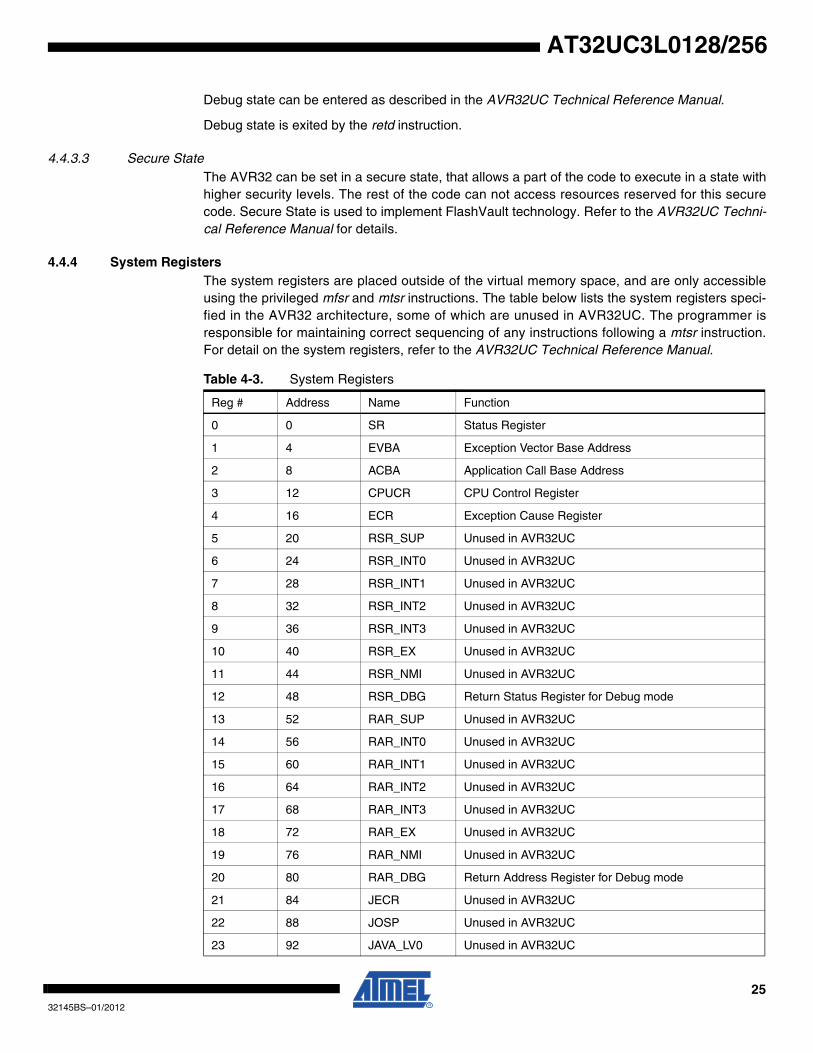
4.4.4 System RegistersThe system registers are placed outside of the virtual memory space, and are only accessibleusing the privileged mfsr and mtsr instructions. The table below lists the system registers speci-fied in the AVR32 architecture, some of which are unused in AVR32UC. The programmer isresponsible for maintaining correct sequencing of any instructions following a mtsr instruction.For detail on the system registers, refer to the AVR32UC Technical Reference Manual.
Table 4-3. System Registers
Reg # Address Name Function
0 0 SR Status Register
1 4 EVBA Exception Vector Base Address
2 8 ACBA Application Call Base Address
3 12 CPUCR CPU Control Register
4 16 ECR Exception Cause Register
5 20 RSR_SUP Unused in AVR32UC
6 24 RSR_INT0 Unused in AVR32UC
7 28 RSR_INT1 Unused in AVR32UC
8 32 RSR_INT2 Unused in AVR32UC
9 36 RSR_INT3 Unused in AVR32UC
10 40 RSR_EX Unused in AVR32UC
11 44 RSR_NMI Unused in AVR32UC
12 48 RSR_DBG Return Status Register for Debug mode
13 52 RAR_SUP Unused in AVR32UC
14 56 RAR_INT0 Unused in AVR32UC
15 60 RAR_INT1 Unused in AVR32UC
16 64 RAR_INT2 Unused in AVR32UC
17 68 RAR_INT3 Unused in AVR32UC
18 72 RAR_EX Unused in AVR32UC
19 76 RAR_NMI Unused in AVR32UC
20 80 RAR_DBG Return Address Register for Debug mode
21 84 JECR Unused in AVR32UC
22 88 JOSP Unused in AVR32UC
23 92 JAVA_LV0 Unused in AVR32UC
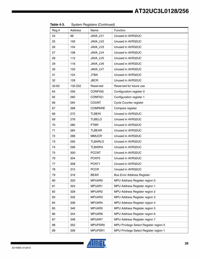
2632145BS–01/2012
AT32UC3L0128/256
24 96 JAVA_LV1 Unused in AVR32UC
25 100 JAVA_LV2 Unused in AVR32UC
26 104 JAVA_LV3 Unused in AVR32UC
27 108 JAVA_LV4 Unused in AVR32UC
28 112 JAVA_LV5 Unused in AVR32UC
29 116 JAVA_LV6 Unused in AVR32UC
30 120 JAVA_LV7 Unused in AVR32UC
31 124 JTBA Unused in AVR32UC
32 128 JBCR Unused in AVR32UC
33-63 132-252 Reserved Reserved for future use
64 256 CONFIG0 Configuration register 0
65 260 CONFIG1 Configuration register 1
66 264 COUNT Cycle Counter register
67 268 COMPARE Compare register
68 272 TLBEHI Unused in AVR32UC
69 276 TLBELO Unused in AVR32UC
70 280 PTBR Unused in AVR32UC
71 284 TLBEAR Unused in AVR32UC
72 288 MMUCR Unused in AVR32UC
73 292 TLBARLO Unused in AVR32UC
74 296 TLBARHI Unused in AVR32UC
75 300 PCCNT Unused in AVR32UC
76 304 PCNT0 Unused in AVR32UC
77 308 PCNT1 Unused in AVR32UC
78 312 PCCR Unused in AVR32UC
79 316 BEAR Bus Error Address Register
80 320 MPUAR0 MPU Address Register region 0
81 324 MPUAR1 MPU Address Register region 1
82 328 MPUAR2 MPU Address Register region 2
83 332 MPUAR3 MPU Address Register region 3
84 336 MPUAR4 MPU Address Register region 4
85 340 MPUAR5 MPU Address Register region 5
86 344 MPUAR6 MPU Address Register region 6
87 348 MPUAR7 MPU Address Register region 7
88 352 MPUPSR0 MPU Privilege Select Register region 0
89 356 MPUPSR1 MPU Privilege Select Register region 1
Table 4-3. System Registers (Continued)
Reg # Address Name Function

2732145BS–01/2012
AT32UC3L0128/256
4.5 Exceptions and InterruptsIn the AVR32 architecture, events are used as a common term for exceptions and interrupts.AVR32UC incorporates a powerful event handling scheme. The different event sources, like Ille-gal Op-code and interrupt requests, have different priority levels, ensuring a well-definedbehavior when multiple events are received simultaneously. Additionally, pending events of ahigher priority class may preempt handling of ongoing events of a lower priority class.
When an event occurs, the execution of the instruction stream is halted, and execution is passedto an event handler at an address specified in Table 4-4 on page 31. Most of the handlers areplaced sequentially in the code space starting at the address specified by EVBA, with four bytesbetween each handler. This gives ample space for a jump instruction to be placed there, jump-ing to the event routine itself. A few critical handlers have larger spacing between them, allowingthe entire event routine to be placed directly at the address specified by the EVBA-relative offsetgenerated by hardware. All interrupt sources have autovectored interrupt service routine (ISR)addresses. This allows the interrupt controller to directly specify the ISR address as an address
90 360 MPUPSR2 MPU Privilege Select Register region 2
91 364 MPUPSR3 MPU Privilege Select Register region 3
92 368 MPUPSR4 MPU Privilege Select Register region 4
93 372 MPUPSR5 MPU Privilege Select Register region 5
94 376 MPUPSR6 MPU Privilege Select Register region 6
95 380 MPUPSR7 MPU Privilege Select Register region 7
96 384 MPUCRA Unused in this version of AVR32UC
97 388 MPUCRB Unused in this version of AVR32UC
98 392 MPUBRA Unused in this version of AVR32UC
99 396 MPUBRB Unused in this version of AVR32UC
100 400 MPUAPRA MPU Access Permission Register A
101 404 MPUAPRB MPU Access Permission Register B
102 408 MPUCR MPU Control Register
103 412 SS_STATUS Secure State Status Register
104 416 SS_ADRF Secure State Address Flash Register
105 420 SS_ADRR Secure State Address RAM Register
106 424 SS_ADR0 Secure State Address 0 Register
107 428 SS_ADR1 Secure State Address 1 Register
108 432 SS_SP_SYS Secure State Stack Pointer System Register
109 436 SS_SP_APP Secure State Stack Pointer Application Register
110 440 SS_RAR Secure State Return Address Register
111 444 SS_RSR Secure State Return Status Register
112-191 448-764 Reserved Reserved for future use
192-255 768-1020 IMPL IMPLEMENTATION DEFINED
Table 4-3. System Registers (Continued)
Reg # Address Name Function

2832145BS–01/2012
AT32UC3L0128/256
relative to EVBA. The autovector offset has 14 address bits, giving an offset of maximum 16384bytes. The target address of the event handler is calculated as (EVBA | event_handler_offset),not (EVBA + event_handler_offset), so EVBA and exception code segments must be set upappropriately. The same mechanisms are used to service all different types of events, includinginterrupt requests, yielding a uniform event handling scheme.
An interrupt controller does the priority handling of the interrupts and provides the autovector off-set to the CPU.
4.5.1 System Stack IssuesEvent handling in AVR32UC uses the system stack pointed to by the system stack pointer,SP_SYS, for pushing and popping R8-R12, LR, status register, and return address. Since eventcode may be timing-critical, SP_SYS should point to memory addresses in the IRAM section,since the timing of accesses to this memory section is both fast and deterministic.
The user must also make sure that the system stack is large enough so that any event is able topush the required registers to stack. If the system stack is full, and an event occurs, the systemwill enter an UNDEFINED state.
4.5.2 Exceptions and Interrupt RequestsWhen an event other than scall or debug request is received by the core, the following actionsare performed atomically:
1. The pending event will not be accepted if it is masked. The I3M, I2M, I1M, I0M, EM, and GM bits in the Status Register are used to mask different events. Not all events can be masked. A few critical events (NMI, Unrecoverable Exception, TLB Multiple Hit, and Bus Error) can not be masked. When an event is accepted, hardware automatically sets the mask bits corresponding to all sources with equal or lower priority. This inhibits acceptance of other events of the same or lower priority, except for the critical events listed above. Software may choose to clear some or all of these bits after saving the necessary state if other priority schemes are desired. It is the event source’s respons-ability to ensure that their events are left pending until accepted by the CPU.
2. When a request is accepted, the Status Register and Program Counter of the current context is stored to the system stack. If the event is an INT0, INT1, INT2, or INT3, reg-isters R8-R12 and LR are also automatically stored to stack. Storing the Status Register ensures that the core is returned to the previous execution mode when the current event handling is completed. When exceptions occur, both the EM and GM bits are set, and the application may manually enable nested exceptions if desired by clear-ing the appropriate bit. Each exception handler has a dedicated handler address, and this address uniquely identifies the exception source.
3. The Mode bits are set to reflect the priority of the accepted event, and the correct regis-ter file bank is selected. The address of the event handler, as shown in Table 4-4 on page 31, is loaded into the Program Counter.
The execution of the event handler routine then continues from the effective address calculated.
The rete instruction signals the end of the event. When encountered, the Return Status Registerand Return Address Register are popped from the system stack and restored to the Status Reg-ister and Program Counter. If the rete instruction returns from INT0, INT1, INT2, or INT3,registers R8-R12 and LR are also popped from the system stack. The restored Status Registercontains information allowing the core to resume operation in the previous execution mode. Thisconcludes the event handling.

2932145BS–01/2012
AT32UC3L0128/256
4.5.3 Supervisor CallsThe AVR32 instruction set provides a supervisor mode call instruction. The scall instruction isdesigned so that privileged routines can be called from any context. This facilitates sharing ofcode between different execution modes. The scall mechanism is designed so that a minimalexecution cycle overhead is experienced when performing supervisor routine calls from time-critical event handlers.
The scall instruction behaves differently depending on which mode it is called from. The behav-iour is detailed in the instruction set reference. In order to allow the scall routine to return to thecorrect context, a return from supervisor call instruction, rets, is implemented. In the AVR32UCCPU, scall and rets uses the system stack to store the return address and the status register.
4.5.4 Debug RequestsThe AVR32 architecture defines a dedicated Debug mode. When a debug request is received bythe core, Debug mode is entered. Entry into Debug mode can be masked by the DM bit in thestatus register. Upon entry into Debug mode, hardware sets the SR.D bit and jumps to theDebug Exception handler. By default, Debug mode executes in the exception context, but withdedicated Return Address Register and Return Status Register. These dedicated registersremove the need for storing this data to the system stack, thereby improving debuggability. TheMode bits in the Status Register can freely be manipulated in Debug mode, to observe registersin all contexts, while retaining full privileges.
Debug mode is exited by executing the retd instruction. This returns to the previous context.
4.5.5 Entry Points for EventsSeveral different event handler entry points exist. In AVR32UC, the reset address is0x80000000. This places the reset address in the boot flash memory area.
TLB miss exceptions and scall have a dedicated space relative to EVBA where their event han-dler can be placed. This speeds up execution by removing the need for a jump instruction placedat the program address jumped to by the event hardware. All other exceptions have a dedicatedevent routine entry point located relative to EVBA. The handler routine address identifies theexception source directly.
AVR32UC uses the ITLB and DTLB protection exceptions to signal a MPU protection violation.ITLB and DTLB miss exceptions are used to signal that an access address did not map to any ofthe entries in the MPU. TLB multiple hit exception indicates that an access address did map tomultiple TLB entries, signalling an error.
All interrupt requests have entry points located at an offset relative to EVBA. This autovector off-set is specified by an interrupt controller. The programmer must make sure that none of theautovector offsets interfere with the placement of other code. The autovector offset has 14address bits, giving an offset of maximum 16384 bytes.
Special considerations should be made when loading EVBA with a pointer. Due to security con-siderations, the event handlers should be located in non-writeable flash memory, or optionally ina privileged memory protection region if an MPU is present.
If several events occur on the same instruction, they are handled in a prioritized way. The priorityordering is presented in Table 4-4 on page 31. If events occur on several instructions at differentlocations in the pipeline, the events on the oldest instruction are always handled before anyevents on any younger instruction, even if the younger instruction has events of higher priority

3032145BS–01/2012
AT32UC3L0128/256
than the oldest instruction. An instruction B is younger than an instruction A if it was sent downthe pipeline later than A.
The addresses and priority of simultaneous events are shown in Table 4-4 on page 31. Some ofthe exceptions are unused in AVR32UC since it has no MMU, coprocessor interface, or floating-point unit.

3132145BS–01/2012
AT32UC3L0128/256
Table 4-4. Priority and Handler Addresses for Events
Priority Handler Address Name Event source Stored Return Address
1 0x80000000 Reset External input Undefined
2 Provided by OCD system OCD Stop CPU OCD system First non-completed instruction
3 EVBA+0x00 Unrecoverable exception Internal PC of offending instruction
4 EVBA+0x04 TLB multiple hit MPU PC of offending instruction
5 EVBA+0x08 Bus error data fetch Data bus First non-completed instruction
6 EVBA+0x0C Bus error instruction fetch Data bus First non-completed instruction
7 EVBA+0x10 NMI External input First non-completed instruction
8 Autovectored Interrupt 3 request External input First non-completed instruction
9 Autovectored Interrupt 2 request External input First non-completed instruction
10 Autovectored Interrupt 1 request External input First non-completed instruction
11 Autovectored Interrupt 0 request External input First non-completed instruction
12 EVBA+0x14 Instruction Address CPU PC of offending instruction
13 EVBA+0x50 ITLB Miss MPU PC of offending instruction
14 EVBA+0x18 ITLB Protection MPU PC of offending instruction
15 EVBA+0x1C Breakpoint OCD system First non-completed instruction
16 EVBA+0x20 Illegal Opcode Instruction PC of offending instruction
17 EVBA+0x24 Unimplemented instruction Instruction PC of offending instruction
18 EVBA+0x28 Privilege violation Instruction PC of offending instruction
19 EVBA+0x2C Floating-point UNUSED
20 EVBA+0x30 Coprocessor absent Instruction PC of offending instruction
21 EVBA+0x100 Supervisor call Instruction PC(Supervisor Call) +2
22 EVBA+0x34 Data Address (Read) CPU PC of offending instruction
23 EVBA+0x38 Data Address (Write) CPU PC of offending instruction
24 EVBA+0x60 DTLB Miss (Read) MPU PC of offending instruction
25 EVBA+0x70 DTLB Miss (Write) MPU PC of offending instruction
26 EVBA+0x3C DTLB Protection (Read) MPU PC of offending instruction
27 EVBA+0x40 DTLB Protection (Write) MPU PC of offending instruction
28 EVBA+0x44 DTLB Modified UNUSED

3232145BS–01/2012
AT32UC3L0128/256
5. Memories
5.1 Embedded Memories• Internal high-speed flash
– 256Kbytes (AT32UC3L0256)– 128Kbytes (AT32UC3L0128)
• 0 wait state access at up to 25MHz in worst case conditions• 1 wait state access at up to 50MHz in worst case conditions• Pipelined flash architecture, allowing burst reads from sequential flash locations, hiding
penalty of 1 wait state access• Pipelined flash architecture typically reduces the cycle penalty of 1 wait state operation
to only 8% compared to 0 wait state operation• 100 000 write cycles, 15-year data retention capability• Sector lock capabilities, bootloader protection, security bit• 32 fuses, erased during chip erase• User page for data to be preserved during chip erase
• Internal high-speed SRAM, single-cycle access at full speed– 32Kbytes
5.2 Physical Memory MapThe system bus is implemented as a bus matrix. All system bus addresses are fixed, and theyare never remapped in any way, not even during boot. Note that AVR32 UC CPU uses unseg-mented translation, as described in the AVR32 Architecture Manual. The 32-bit physical addressspace is mapped as follows:
Table 5-1. AT32UC3L0128/256 Physical Memory Map
Device Start AddressSize
AT32UC3L0256 AT32UC3L0128
Embedded SRAM 0x00000000 32Kbytes 32Kbytes
Embedded Flash 0x80000000 256Kbytes 128Kbytes
SAU Channels 0x90000000 256 bytes 256 bytes
HSB-PB Bridge B 0xFFFE0000 64Kbytes 64Kbytes
HSB-PB Bridge A 0xFFFF0000 64Kbytes 64Kbytes
Table 5-2. Flash Memory Parameters
Part Number Flash Size (FLASH_PW)Number of pages
(FLASH_P)Page size
(FLASH_W)
AT32UC3L0256 256Kbytes 512 512bytes
AT32UC3L0128 128Kbytes 256 512bytes

3332145BS–01/2012
AT32UC3L0128/256
5.3 Peripheral Address Map
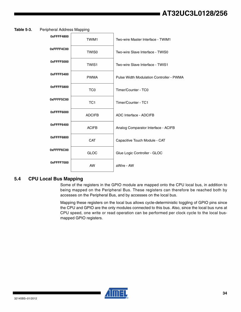
Table 5-3. Peripheral Address Mapping
Address Peripheral Name
0xFFFE0000FLASHCDW Flash Controller - FLASHCDW
0xFFFE0400HMATRIX HSB Matrix - HMATRIX
0xFFFE0800SAU Secure Access Unit - SAU
0xFFFF0000PDCA Peripheral DMA Controller - PDCA
0xFFFF1000INTC Interrupt controller - INTC
0xFFFF1400PM Power Manager - PM
0xFFFF1800SCIF System Control Interface - SCIF
0xFFFF1C00AST Asynchronous Timer - AST
0xFFFF2000WDT Watchdog Timer - WDT
0xFFFF2400EIC External Interrupt Controller - EIC
0xFFFF2800FREQM Frequency Meter - FREQM
0xFFFF2C00GPIO General-Purpose Input/Output Controller - GPIO
0xFFFF3000USART0
Universal Synchronous Asynchronous Receiver Transmitter - USART0
0xFFFF3400USART1
Universal Synchronous Asynchronous Receiver Transmitter - USART1
0xFFFF3800USART2
Universal Synchronous Asynchronous Receiver Transmitter - USART2
0xFFFF3C00USART3
Universal Synchronous Asynchronous Receiver Transmitter - USART3
0xFFFF4000SPI Serial Peripheral Interface - SPI
0xFFFF4400TWIM0 Two-wire Master Interface - TWIM0
3432145BS–01/2012
AT32UC3L0128/256
5.4 CPU Local Bus MappingSome of the registers in the GPIO module are mapped onto the CPU local bus, in addition tobeing mapped on the Peripheral Bus. These registers can therefore be reached both byaccesses on the Peripheral Bus, and by accesses on the local bus.
Mapping these registers on the local bus allows cycle-deterministic toggling of GPIO pins sincethe CPU and GPIO are the only modules connected to this bus. Also, since the local bus runs atCPU speed, one write or read operation can be performed per clock cycle to the local bus-mapped GPIO registers.
0xFFFF4800TWIM1 Two-wire Master Interface - TWIM1
0xFFFF4C00TWIS0 Two-wire Slave Interface - TWIS0
0xFFFF5000TWIS1 Two-wire Slave Interface - TWIS1
0xFFFF5400PWMA Pulse Width Modulation Controller - PWMA
0xFFFF5800TC0 Timer/Counter - TC0
0xFFFF5C00TC1 Timer/Counter - TC1
0xFFFF6000ADCIFB ADC Interface - ADCIFB
0xFFFF6400ACIFB Analog Comparator Interface - ACIFB
0xFFFF6800CAT Capacitive Touch Module - CAT
0xFFFF6C00GLOC Glue Logic Controller - GLOC
0xFFFF7000AW aWire - AW
Table 5-3. Peripheral Address Mapping

3532145BS–01/2012
AT32UC3L0128/256
The following GPIO registers are mapped on the local bus:
Table 5-4. Local Bus Mapped GPIO Registers
Port Register ModeLocal Bus Address Access
0 Output Driver Enable Register (ODER) WRITE 0x40000040 Write-only
SET 0x40000044 Write-only
CLEAR 0x40000048 Write-only
TOGGLE 0x4000004C Write-only
Output Value Register (OVR) WRITE 0x40000050 Write-only
SET 0x40000054 Write-only
CLEAR 0x40000058 Write-only
TOGGLE 0x4000005C Write-only
Pin Value Register (PVR) - 0x40000060 Read-only
1 Output Driver Enable Register (ODER) WRITE 0x40000140 Write-only
SET 0x40000144 Write-only
CLEAR 0x40000148 Write-only
TOGGLE 0x4000014C Write-only
Output Value Register (OVR) WRITE 0x40000150 Write-only
SET 0x40000154 Write-only
CLEAR 0x40000158 Write-only
TOGGLE 0x4000015C Write-only
Pin Value Register (PVR) - 0x40000160 Read-only
3632145BS–01/2012
AT32UC3L0128/256
6. Supply and Startup Considerations
6.1 Supply Considerations
6.1.1 Power SuppliesThe AT32UC3L0128/256 has several types of power supply pins:
•VDDIO: Powers I/O lines. Voltage is 1.8 to 3.3V nominal.
•VDDIN: Powers I/O lines and the internal regulator. Voltage is 1.8 to 3.3V nominal.
•VDDANA: Powers the ADC. Voltage is 1.8V nominal.
•VDDCORE: Powers the core, memories, and peripherals. Voltage is 1.8V nominal.
The ground pins GND are common to VDDCORE, VDDIO, and VDDIN. The ground pin forVDDANA is GNDANA.
When VDDCORE is not connected to VDDIN, the VDDIN voltage must be higher than 1.98V.
Refer to Section 7. on page 41 for power consumption on the various supply pins.
For decoupling recommendations for the different power supplies, please refer to the schematicchecklist.
Refer to Section 3.2 on page 8 for power supply connections for I/O pins.
6.1.2 Voltage RegulatorThe AT32UC3L0128/256 embeds a voltage regulator that converts from 3.3V nominal to 1.8Vwith a load of up to 60mA. The regulator supplies the output voltage on VDDCORE. The regula-tor may only be used to drive internal circuitry in the device. VDDCORE should be externallyconnected to the 1.8V domains. See Section 6.1.3 for regulator connection figures.
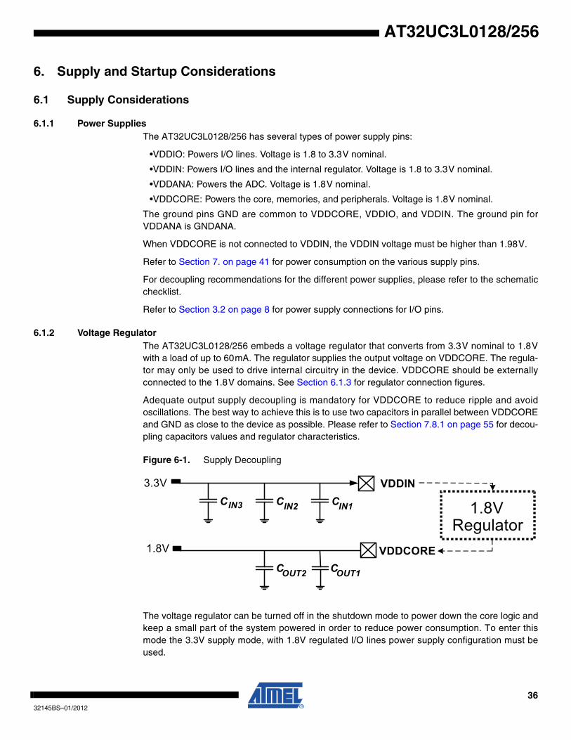
Adequate output supply decoupling is mandatory for VDDCORE to reduce ripple and avoidoscillations. The best way to achieve this is to use two capacitors in parallel between VDDCOREand GND as close to the device as possible. Please refer to Section 7.8.1 on page 55 for decou-pling capacitors values and regulator characteristics.
Figure 6-1. Supply Decoupling
The voltage regulator can be turned off in the shutdown mode to power down the core logic andkeep a small part of the system powered in order to reduce power consumption. To enter thismode the 3.3V supply mode, with 1.8V regulated I/O lines power supply configuration must beused.
3.3V
1.8V
VDDIN
VDDCORE
1.8VRegulator
CIN1
COUT1COUT2
CIN2IN3C

3732145BS–01/2012
AT32UC3L0128/256
6.1.3 Regulator ConnectionThe AT32UC3L0128/256 supports three power supply configurations:
• 3.3V single supply mode
– Shutdown mode is not available
• 1.8V single supply mode
– Shutdown mode is not available
• 3.3V supply mode, with 1.8V regulated I/O lines
– Shutdown mode is available
6.1.3.1 3.3V Single Supply ModeIn 3.3V single supply mode the internal regulator is connected to the 3.3V source (VDDIN pin)and its output feeds VDDCORE. Figure 6-2 shows the power schematics to be used for 3.3Vsingle supply mode. All I/O lines will be powered by the same power (VDDIN=VDDIO).
Figure 6-2. 3.3V Single Supply Mode
VDDIO
VDDCORE
+
-1.98-3.6V
VDDANA ADC
VDDIN GND
GNDANA
CPU, Peripherals, Memories,
SCIF, BOD, RCSYS,
DFLL, PLL
OSC32K,RC32K,POR33,SM33
I/O Pins I/O Pins
OSC32K_2,AST, Wake,Regulator
control
Linear regulator

3832145BS–01/2012
AT32UC3L0128/256
6.1.3.2 1.8 V Single Supply ModeIn 1.8V single supply mode the internal regulator is not used, and VDDIO and VDDCORE arepowered by a single 1.8 V supply as shown in Figure 6-3. All I/O lines will be powered by thesame power (VDDIN = VDDIO = VDDCORE).
Figure 6-3. 1.8V Single Supply Mode.
VDDIO
VDDCORE
+
-1.62-1.98V
VDDANA ADC
VDDIN GND
GNDANA
CPU, Peripherals, Memories,
SCIF, BOD, RCSYS,
DFLL, PLL
OSC32K,RC32K,POR33,SM33
I/O Pins I/O Pins
OSC32K_2,AST, Wake,Regulator
control

3932145BS–01/2012
AT32UC3L0128/256
6.1.3.3 3.3V Supply Mode with 1.8V Regulated I/O LinesIn this mode, the internal regulator is connected to the 3.3V source and its output is connectedto both VDDCORE and VDDIO as shown in Figure 6-4. This configuration is required in order touse Shutdown mode.
Figure 6-4. 3.3V Supply Mode with 1.8V Regulated I/O Lines
In this mode, some I/O lines are powered by VDDIN while other I/O lines are powered by VDDIO.Refer to Section 3.2.1 on page 8 for description of power supply for each I/O line.
Refer to the Power Manager chapter for a description of what parts of the system are powered inShutdown mode.
Important note: As the regulator has a maximum output current of 60 mA, this mode can only beused in applications where the maximum I/O current is known and compatible with the core andperipheral power consumption. Typically, great care must be used to ensure that only a few I/Olines are toggling at the same time and drive very small loads.
VDDIO
VDDCORE
+
-1.98-3.6V
VDDANA ADC
VDDIN GND
GNDANA
CPU, Peripherals, Memories,
SCIF, BOD, RCSYS,
DFLL, PLL
OSC32K,RC32K,POR33,SM33
I/O Pins I/O Pins
OSC32K_2,AST, Wake,Regulator
control
Linear regulator

4032145BS–01/2012
AT32UC3L0128/256
6.1.4 Power-up Sequence
6.1.4.1 Maximum Rise RateTo avoid risk of latch-up, the rise rate of the power supplies must not exceed the valuesdescribed in Table 7-3 on page 42.
Recommended order for power supplies is also described in this chapter.
6.1.4.2 Minimum Rise RateThe integrated Power-on Reset (POR33) circuitry monitoring the VDDIN powering supplyrequires a minimum rise rate for the VDDIN power supply.
See Table 7-3 on page 42 for the minimum rise rate value.
If the application can not ensure that the minimum rise rate condition for the VDDIN power sup-ply is met, one of the following configurations can be used:
• A logic “0” value is applied during power-up on pin PA11 (WAKE_N) until VDDIN rises above 1.2V.
• A logic “0” value is applied during power-up on pin RESET_N until VDDIN rises above 1.2V.
6.2 Startup ConsiderationsThis chapter summarizes the boot sequence of the AT32UC3L0128/256. The behavior afterpower-up is controlled by the Power Manager. For specific details, refer to the Power Managerchapter.
6.2.1 Starting of ClocksAfter power-up, the device will be held in a reset state by the Power-on Reset (POR18 andPOR33) circuitry for a short time to allow the power to stabilize throughout the device. Afterreset, the device will use the System RC Oscillator (RCSYS) as clock source. Please refer toTable 7-17 on page 54 for the frequency for this oscillator.
On system start-up, all high-speed clocks are disabled. All clocks to all modules are running. Noclocks have a divided frequency; all parts of the system receive a clock with the same frequencyas the System RC Oscillator.
When powering up the device, there may be a delay before the voltage has stabilized, depend-ing on the rise time of the supply used. The CPU can start executing code as soon as the supplyis above the POR18 and POR33 thresholds, and before the supply is stable. Before switching toa high-speed clock source, the user should use the BOD to make sure the VDDCORE is abovethe minimum level (1.62V).
6.2.2 Fetching of Initial InstructionsAfter reset has been released, the AVR32 UC CPU starts fetching instructions from the resetaddress, which is 0x80000000. This address points to the first address in the internal Flash.
The code read from the internal flash is free to configure the clock system and clock sources.Please refer to the PM and SCIF chapters for more details.
4132145BS–01/2012
AT32UC3L0128/256
7. Electrical Characteristics
7.1 Absolute Maximum Ratings*
Notes: 1. 5V tolerant pins, see Section 3.2 ”Peripheral Multiplexing on I/O Lines” on page 8
2. VVDD corresponds to either VVDDIN or VVDDIO, depending on the supply for the pin. Refer to Section 3.2 on page 8 for details.
7.2 Supply CharacteristicsThe following characteristics are applicable to the operating temperature range: TA=-40°C to85°C, unless otherwise specified and are valid for a junction temperature up to TJ=100°C.Please refer to Section 6. ”Supply and Startup Considerations” on page 36
Table 7-1. Absolute Maximum Ratings
Operating temperature..................................... -40°C to +85°C *NOTICE: Stresses beyond those listed under “Absolute Maximum Ratings” may cause permanent damage to the device. This is a stress rating only and functional opera-tion of the device at these or other condi-tions beyond those indicated in the operational sections of this specification is not implied. Exposure to absolute maxi-mum rating conditions for extended peri-ods may affect device reliability.
Storage temperature...................................... -60°C to +150°C
Voltage on input pins (except for 5V pins) with respect to ground.................................................................-0.3V to VVDD
(2)+0.3V
Voltage on 5V tolerant(1) pins with respect to ground ............... .............................................................................-0.3V to 5.5V
Total DC output current on all I/O pins - VDDIO ........... 120mA
Total DC output current on all I/O pins - VDDIN ............. 36mA
Maximum operating voltage VDDCORE......................... 1.98V
Maximum operating voltage VDDIO, VDDIN .................... 3.6V
Table 7-2. Supply Characteristics
Symbol Parameter
Voltage
Min Max Unit
VVDDIO DC supply peripheral I/Os 1.62 3.6 V
VVDDIN
DC supply peripheral I/Os, 1.8V single supply mode
1.62 1.98 V
DC supply peripheral I/Os and internal regulator, 3.3V supply mode
1.98 3.6 V
VVDDCORE DC supply core 1.62 1.98 V
VVDDANA Analog supply voltage 1.62 1.98 V

4232145BS–01/2012
AT32UC3L0128/256
Note: 1. These values are based on simulation and characterization of other AVR microcontrollers manufactured in the same process technology. These values are not covered by test limits in production.
7.3 Maximum Clock FrequenciesThese parameters are given in the following conditions:
• VVDDCORE = 1.62V to 1.98V
• Temperature = -40°C to 85°C
7.4 Power ConsumptionThe values in Table 7-5 are measured values of power consumption under the following condi-tions, except where noted:
• Operating conditions, internal core supply (Figure 7-1) - this is the default configuration
Table 7-3. Supply Rise Rates and Order(1)
Symbol Parameter
Rise Rate
Min Max Unit Comment
VVDDIO DC supply peripheral I/Os 0 2.5 V/µs
VVDDINDC supply peripheral I/Os and internal regulator
0.002 2.5 V/µsSlower rise time requires external power-on reset circuit.
VVDDCORE DC supply core 0 2.5 V/µsRise before or at the same time as VDDIO
VVDDANA Analog supply voltage 0 2.5 V/µsRise together with VDDCORE
Table 7-4. Clock Frequencies
Symbol Parameter Description Min Max Units
fCPU CPU clock frequency 50
MHz
fPBA PBA clock frequency 50
fPBB PBB clock frequency 50
fGCLK0 GCLK0 clock frequency DFLLIF main reference, GCLK0 pin 50
fGCLK1 GCLK1 clock frequencyDFLLIF dithering and SSG reference, GCLK1 pin
50
fGCLK2 GCLK2 clock frequency AST, GCLK2 pin 20
fGCLK3 GCLK3 clock frequency PWMA, GCLK3 pin 140
fGCLK4 GCLK4 clock frequency CAT, ACIFB, GCLK4 pin 50
fGCLK5 GCLK5 clock frequency GLOC 80
fGCLK6 GCLK6 clock frequency 50
fGCLK7 GCLK7 clock frequency 50
fGCLK8 GCLK8 clock frequency PLL source clock 50
fGCLK9 GCLK9 clock frequency FREQM, GCLK0-8 150
4332145BS–01/2012
AT32UC3L0128/256
– VVDDIN = 3.0V
– VVDDCORE = 1.62V, supplied by the internal regulator
– Corresponds to the 3.3V supply mode with 1.8V regulated I/O lines, please refer to the Supply and Startup Considerations section for more details
• Equivalent to the 3.3V single supply mode
• Consumption in 1.8V single supply mode can be estimated by subtracting the regula-
tor static current
• Operating conditions, external core supply (Figure 7-2) - used only when noted
– VVDDIN = VVDDCORE = 1.8V
– Corresponds to the 1.8V single supply mode, please refer to the Supply and Startup Considerations section for more details
• TA = 25°C• Oscillators
– OSC0 (crystal oscillator) stopped
– OSC32K (32KHz crystal oscillator) running with external 32KHz crystal
– DFLL running at 50MHz with OSC32K as reference
• Clocks
– DFLL used as main clock source
– CPU, HSB, and PBB clocks undivided
– PBA clock divided by 4
– The following peripheral clocks running
• PM, SCIF, AST, FLASHCDW, PBA bridge
– All other peripheral clocks stopped
• I/Os are inactive with internal pull-up
• Flash enabled in high speed mode
• POR18 enabled
• POR33 disabled

4432145BS–01/2012
AT32UC3L0128/256
Note: 1. These numbers are valid for the measured condition only and must not be extrapolated to other frequencies.
Figure 7-1. Measurement Schematic, Internal Core Supply
Table 7-5. Power Consumption for Different Operating Modes
Mode Conditions Measured on Consumption Typ Unit
Active(1)CPU running a recursive Fibonacci algorithm
Amp0
300
µA/MHz
CPU running a division algorithm 174
Idle(1) 96
Frozen(1) 57
Standby(1) 46
Stop 38
µA
DeepStop 25
Static
-OSC32K and AST stopped
-Internal core supply14
-OSC32K running
-AST running at 1KHz
-External core supply (Figure 7-2)
7.3
-OSC32K and AST stopped
-External core supply (Figure 7-2)6.7
Shutdown
-OSC32K running
-AST running at 1KHz800
nA
AST and OSC32K stopped 220
Amp0 VDDIN
VDDCORE
VDDANA
VDDIO

4532145BS–01/2012
AT32UC3L0128/256
Figure 7-2. Measurement Schematic, External Core Supply
Amp0 VDDIN
VDDCORE
VDDANA
VDDIO

4632145BS–01/2012
AT32UC3L0128/256
7.5 I/O Pin Characteristics
Notes: 1. VVDD corresponds to either VVDDIN or VVDDIO, depending on the supply for the pin. Refer to Section 3.2.1 on page 8 for details.
2. These values are based on simulation and characterization of other AVR microcontrollers manufactured in the same pro-cess technology. These values are not covered by test limits in production.
Table 7-6. Normal I/O Pin Characteristics(1)
Symbol Parameter Condition Min Typ Max Units
RPULLUP Pull-up resistance 75 100 145 kOhm
VIL Input low-level voltageVVDD = 3.0V -0.3 0.3*VVDD
VVVDD = 1.62V -0.3 0.3*VVDD
VIH Input high-level voltageVVDD = 3.6V 0.7*VVDD VVDD + 0.3
VVVDD = 1.98V 0.7*VVDD VVDD + 0.3
VOL Output low-level voltageVVDD = 3.0V, IOL = 3mA 0.4
VVVDD = 1.62V, IOL = 2mA 0.4
VOH Output high-level voltageVVDD = 3.0V, IOH = 3mA VVDD - 0.4
VVVDD = 1.62V, IOH = 2mA VVDD - 0.4
fMAX Output frequency(2)VVDD = 3.0V, load = 10pF 45
MHzVVDD = 3.0V, load = 30pF 23
tRISE Rise time(2)VVDD = 3.0V, load = 10pF 4.7
nsVVDD = 3.0V, load = 30pF 11.5
tFALL Fall time(2)VVDD = 3.0V, load = 10pF 4.8
VVDD = 3.0V, load = 30pF 12
ILEAK Input leakage current Pull-up resistors disabled 1 µA
CIN
Input capacitance, all normal I/O pins except PA05, PA07, PA17, PA20, PA21, PB04, PB05
TQFP48 package 1.4
pF
QFN48 package 1.1
TLLGA48 package 1.1
CIN Input capacitance, PA20
TQFP48 package 2.7
QFN48 package 2.4
TLLGA48 package 2.4
CIN
Input capacitance, PA05, PA07, PA17, PA21, PB04, PB05
TQFP48 package 3.8
QFN48 package 3.5
TLLGA48 package 3.5
Table 7-7. High-drive I/O Pin Characteristics(1)
Symbol Parameter Condition Min Typ Max Units
RPULLUP Pull-up resistance
PA06 30 50 110
kOhmPA02, PB01, RESET 75 100 145
PA08, PA09 10 20 45

4732145BS–01/2012
AT32UC3L0128/256
Notes: 1. VVDD corresponds to either VVDDIN or VVDDIO, depending on the supply for the pin. Refer to Section 3.2.1 on page 8 for details.
2. These values are based on simulation and characterization of other AVR microcontrollers manufactured in the same pro-cess technology. These values are not covered by test limits in production.
VIL Input low-level voltageVVDD = 3.0V -0.3 0.3*VVDD
VVVDD = 1.62V -0.3 0.3*VVDD
VIH Input high-level voltageVVDD = 3.6V 0.7*VVDD VVDD + 0.3
VVVDD = 1.98V 0.7*VVDD VVDD + 0.3
VOL Output low-level voltageVVDD = 3.0V, IOL = 6mA 0.4
VVVDD = 1.62V, IOL = 4mA 0.4
VOH Output high-level voltageVVDD = 3.0V, IOH = 6mA VVDD-0.4
VVVDD = 1.62V, IOH = 4mA VVDD-0.4
fMAXOutput frequency, all High-drive I/O pins, except PA08 and PA09(2)
VVDD = 3.0V, load = 10pF 45MHz
VVDD = 3.0V, load = 30pF 23
tRISERise time, all High-drive I/O pins, except PA08 and PA09(2)
VVDD = 3.0V, load = 10pF 4.7
nsVVDD = 3.0V, load = 30pF 11.5
tFALLFall time, all High-drive I/O pins, except PA08 and PA09(2)
VVDD = 3.0V, load = 10pF 4.8
VVDD = 3.0V, load = 30pF 12
fMAXOutput frequency, PA08 and PA09(2)
VVDD = 3.0V, load = 10pF 54MHz
VVDD = 3.0V, load = 30pF 40
tRISE Rise time, PA08 and PA09(2)VVDD = 3.0V, load = 10pF 2.8
nsVVDD = 3.0V, load = 30pF 4.9
tFALL Fall time, PA08 and PA09(2)VVDD = 3.0V, load = 10pF 2.4
VVDD = 3.0V, load = 30pF 4.6
ILEAK Input leakage current Pull-up resistors disabled 1 µA
CINInput capacitance, all High-drive I/O pins, except PA08 and PA09
TQFP48 package 2.2
pF
QFN48 package 2.0
TLLGA48 package 2.0
CIN Input capacitance, PA08 and PA09
TQFP48 package 7.0
QFN48 package 6.7
TLLGA48 package 6.7
Table 7-7. High-drive I/O Pin Characteristics(1)
Symbol Parameter Condition Min Typ Max Units
Table 7-8. High-drive I/O, 5V Tolerant, Pin Characteristics(1)
Symbol Parameter Condition Min Typ Max Units
RPULLUP Pull-up resistance 30 50 110 kOhm
VIL Input low-level voltageVVDD = 3.0V -0.3 0.3*VVDD
VVVDD = 1.62V -0.3 0.3*VVDD

4832145BS–01/2012
AT32UC3L0128/256
Notes: 1. VVDD corresponds to either VVDDIN or VVDDIO, depending on the supply for the pin. Refer to Section 3.2.1 on page 8 for details.
2. These values are based on simulation and characterization of other AVR microcontrollers manufactured in the same pro-cess technology. These values are not covered by test limits in production.
VIH Input high-level voltageVVDD = 3.6V 0.7*VVDD 5.5
VVVDD = 1.98V 0.7*VVDD 5.5
VOL Output low-level voltageVVDD = 3.0V, IOL = 6mA 0.4
VVVDD = 1.62V, IOL = 4mA 0.4
VOH Output high-level voltageVVDD = 3.0V, IOH = 6mA VVDD-0.4
VVVDD = 1.62V, IOH = 4mA VVDD-0.4
fMAX Output frequency(2)VVDD = 3.0V, load = 10pF 87
MHzVVDD = 3.0V, load = 30pF 58
tRISE Rise time(2)VVDD = 3.0V, load = 10pF 2.3
nsVVDD = 3.0V, load = 30pF 4.3
tFALL Fall time(2)VVDD = 3.0V, load = 10pF 1.9
VVDD = 3.0V, load = 30pF 3.7
ILEAK Input leakage current 5.5V, pull-up resistors disabled 10 µA
CIN Input capacitance
TQFP48 package 4.5
pFQFN48 package 4.2
TLLGA48 package 4.2
Table 7-8. High-drive I/O, 5V Tolerant, Pin Characteristics(1)
Symbol Parameter Condition Min Typ Max Units
Table 7-9. TWI Pin Characteristics(1)
Symbol Parameter Condition Min Typ Max Units
RPULLUP Pull-up resistance 25 35 60 kOhm
VIL Input low-level voltageVVDD = 3.0V -0.3 0.3*VVDD
VVVDD = 1.62V -0.3 0.3*VVDD
VIH
Input high-level voltageVVDD = 3.6V 0.7*VVDD VVDD + 0.3
VVVDD = 1.98V 0.7*VVDD VVDD + 0.3
Input high-level voltage, 5V tolerant SMBUS compliant pins
VVDD = 3.6V 0.7*VVDD 5.5V
VVDD = 1.98V 0.7*VVDD 5.5
VOL Output low-level voltage IOL = 3mA 0.4 V
ILEAK Input leakage current Pull-up resistors disabled 1
µAIIL Input low leakage 1
IIH Input high leakage 1
CIN Input capacitance
TQFP48 package 3.8
pFQFN48 package 3.5
TLLGA48 package 3.5

4932145BS–01/2012
AT32UC3L0128/256
Note: 1. VVDD corresponds to either VVDDIN or VVDDIO, depending on the supply for the pin. Refer to Section 3.2.1 on page 8 for details.
7.6 Oscillator Characteristics
7.6.1 Oscillator 0 (OSC0) Characteristics
7.6.1.1 Digital Clock Characteristics
The following table describes the characteristics for the oscillator when a digital clock is appliedon XIN.
Note: 1. These values are based on simulation and characterization of other AVR microcontrollers manufactured in the same pro-cess technology. These values are not covered by test limits in production.
7.6.1.2 Crystal Oscillator Characteristics
The following table describes the characteristics for the oscillator when a crystal is connectedbetween XIN and XOUT as shown in Figure 7-3. The user must choose a crystal oscillatorwhere the crystal load capacitance CL is within the range given in the table. The exact value of CL
can be found in the crystal datasheet. The capacitance of the external capacitors (CLEXT) canthen be computed as follows:
where CPCB is the capacitance of the PCB and Ci is the internal equivalent load capacitance.
tFALL Fall timeCbus = 400pF, VVDD > 2.0V 250
nsCbus = 400pF, VVDD > 1.62V 470
fMAX Max frequency Cbus = 400pF, VVDD > 2.0V 400 kHz
Table 7-9. TWI Pin Characteristics(1)
Symbol Parameter Condition Min Typ Max Units
Table 7-10. Digital Clock Characteristics
Symbol Parameter Conditions Min Typ Max Units
fCPXIN XIN clock frequency 50 MHz
tCPXIN XIN clock duty cycle(1) 40 60 %
tSTARTUP Startup time 0 cycles
CIN XIN input capacitance
TQFP48 package 7.0
pFQFN48 package 6.7
TLLGA48 package 6.7
CLEXT 2 CL Ci–( ) CPCB–=

5032145BS–01/2012
AT32UC3L0128/256
Notes: 1. Please refer to the SCIF chapter for details.2. Nominal crystal cycles.3. These values are based on simulation and characterization of other AVR microcontrollers manufactured in the same pro-
cess technology. These values are not covered by test limits in production.
Figure 7-3. Oscillator Connection
7.6.2 32KHz Crystal Oscillator (OSC32K) CharacteristicsFigure 7-3 and the equation above also applies to the 32KHz oscillator connection. The usermust choose a crystal oscillator where the crystal load capacitance CL is within the range givenin the table. The exact value of CL can then be found in the crystal datasheet.
Table 7-11. Crystal Oscillator Characteristics
Symbol Parameter Conditions Min Typ Max Unit
fOUT Crystal oscillator frequency(3) 0.45 10 16 MHz
CL Crystal load capacitance(3) 6 18pF
Ci Internal equivalent load capacitance 2
tSTARTUP Startup time SCIF.OSCCTRL.GAIN = 2(1) 30 000(2) cycles
IOSC Current consumption
Active mode, f = 0.45MHz, SCIF.OSCCTRL.GAIN = 0
30
µAActive mode, f = 10MHz,
SCIF.OSCCTRL.GAIN = 2220
XIN
XOUT
CLEXT
CLEXT
CLCi
UC3L

5132145BS–01/2012
AT32UC3L0128/256
Notes: 1. Nominal crystal cycles.
2. These values are based on simulation and characterization of other AVR microcontrollers manufactured in the same pro-cess technology. These values are not covered by test limits in production.
7.6.3 Phase Locked Loop (PLL) Characteristics
Note: 1. These values are based on simulation and characterization of other AVR microcontrollers manufactured in the same pro-cess technology. These values are not covered by test limits in production.
Table 7-12. 32 KHz Crystal Oscillator Characteristics
Symbol Parameter Conditions Min Typ Max Unit
fOUT Crystal oscillator frequency 32 768 Hz
tSTARTUP Startup time RS = 60kOhm, CL = 9pF 30 000(1) cycles
CL Crystal load capacitance(2) 6 12.5
pFCi
Internal equivalent load capacitance
2
IOSC32 Current consumption 0.6 µA
RS Equivalent series resistance(2) 32 768Hz 35 85 kOhm
Table 7-13. Phase Locked Loop Characteristics
Symbol Parameter Conditions Min Typ Max Unit
fOUT Output frequency(1) 40 240MHz
fIN Input frequency(1) 4 16
IPLL Current consumption 8 µA/MHz
tSTARTUP
Startup time, from enabling the PLL until the PLL is locked
fIN= 4MHz 200µs
fIN= 16MHz 155

5232145BS–01/2012
AT32UC3L0128/256
7.6.4 Digital Frequency Locked Loop (DFLL) Characteristics
Notes: 1. Spread Spectrum Generator (SSG) is disabled by writing a zero to the EN bit in the DFLL0SSG register.2. These values are based on simulation and characterization of other AVR microcontrollers manufactured in the same pro-
cess technology. These values are not covered by test limits in production.3. The FINE and COARSE values are selected by wrirting to the DFLL0VAL.FINE and DFLL0VAL.COARSE field respectively.
Table 7-14. Digital Frequency Locked Loop Characteristics
Symbol Parameter Conditions Min Typ Max Unit
fOUT Output frequency(2) 20 150 MHz
fREF Reference frequency(2) 8 150 kHz
FINE resolution step FINE > 100, all COARSE values (3) 0.38 %
Frequency drift over voltage and temperature
Open loop modeSee
Figure 7-4
Accuracy(2)
FINE lock, fREF = 32kHz, SSG disabled 0.1 0.5
%
ACCURATE lock, fREF = 32kHz, dither clk RCSYS/2, SSG disabled
0.06 0.5
FINE lock, fREF = 8-150kHz, SSG disabled
0.2 1
ACCURATE lock, fREF = 8-150kHz, dither clk RCSYS/2, SSG disabled
0.1 1
IDFLL Power consumption 25 µA/MHz
tSTARTUP Startup time(2) Within 90% of final values 100 µs
tLOCK Lock time
fREF = 32kHz, FINE lock, SSG disabled 8
msfREF = 32kHz, ACCURATE lock, dithering clock = RCSYS/2, SSG disabled
28

5332145BS–01/2012
AT32UC3L0128/256
Figure 7-4. DFLL Open Loop Frequency Variation(1)(2)
Notes: 1. The plot shows a typical open loop mode behavior with COARSE= 99 and FINE= 255
2. These values are based on simulation and characterization of other AVR microcontrollers manufactured in the same pro-cess technology. These values are not covered by test limits in production.
7.6.5 120MHz RC Oscillator (RC120M) Characteristics
Note: 1. These values are based on simulation and characterization of other AVR microcontrollers manufactured in the same pro-cess technology. These values are not covered by test limits in production.
Table 7-15. Internal 120MHz RC Oscillator Characteristics
Symbol Parameter Conditions Min Typ Max Unit
fOUT Output frequency(1) 88 120 152 MHz
IRC120M Current consumption 1.2 mA
tSTARTUP Startup time(1) VVDDCORE = 1.8V 3 µs
DFLL Open Loop Frequency variation
80
90
100
110
120
130
140
150
160
-40 -20 0 20 40 60 80
Temperature
Freq
uenc
ies
(MH
z)
1,98V1,8V
1.62V

5432145BS–01/2012
AT32UC3L0128/256
7.6.6 32kHz RC Oscillator (RC32K) Characteristics
Note: 1. These values are based on simulation and characterization of other AVR microcontrollers manufactured in the same pro-cess technology. These values are not covered by test limits in production.
7.6.7 System RC Oscillator (RCSYS) Characteristics
7.7 Flash Characteristics
Table 7-18 gives the device maximum operating frequency depending on the number of flashwait states and the flash read mode. The FSW bit in the FLASHCDW FSR register controls thenumber of wait states used when accessing the flash memory.
Table 7-16. 32kHz RC Oscillator Characteristics
Symbol Parameter Conditions Min Typ Max Unit
fOUT Output frequency(1) 20 32 44 kHz
IRC32K Current consumption 0.7 µA
tSTARTUP Startup time(1) 100 µs
Table 7-17. System RC Oscillator Characteristics
Symbol Parameter Conditions Min Typ Max Unit
fOUT Output frequency Calibrated at 85°C 111.6 115 118.4 kHz
Table 7-18. Maximum Operating Frequency
Flash Wait States Read Mode Maximum Operating Frequency
1High speed read mode
50MHz
0 25MHz
1Normal read mode
30MHz
0 15MHz
Table 7-19. Flash Characteristics
Symbol Parameter Conditions Min Typ Max Unit
tFPP Page programming time
fCLK_HSB = 50MHz
5
ms
tFPE Page erase time 5
tFFP Fuse programming time 1
tFEA Full chip erase time (EA) 6
tFCE JTAG chip erase time (CHIP_ERASE) fCLK_HSB = 115kHz 310

5532145BS–01/2012
AT32UC3L0128/256
7.8 Analog Characteristics
7.8.1 Voltage Regulator Characteristics
Note: 1. These values are based on simulation and characterization of other AVR microcontrollers manufactured in the same pro-cess technology. These values are not covered by test limits in production.
Note: 1. Refer to Section 6.1.2 on page 36.
Table 7-20. Flash Endurance and Data Retention
Symbol Parameter Conditions Min Typ Max Unit
NFARRAY Array endurance (write/page) 100kcycles
NFFUSE General Purpose fuses endurance (write/bit) 10k
tRET Data retention 15 years
Table 7-21. VREG Electrical Characteristics
Symbol Parameter Condition Min Typ Max Units
VVDDIN Input voltage range 1.98 3.3 3.6V
VVDDCORE Output voltage, calibrated value VVDDIN >= 1.98V 1.8
Output voltage accuracy(1)
IOUT = 0.1mA to 60mA,
VVDDIN > 1.98V2
%IOUT = 0.1mA to 60mA,
VVDDIN < 1.98V 4
IOUT DC output current(1)Normal mode 60
mALow power mode 1
IVREG Static current of internal regulatorNormal mode 13
µALow power mode 4
Table 7-22. Decoupling Requirements
Symbol Parameter Condition Typ Techno. Units
CIN1 Input regulator capacitor 1 33nF
CIN2 Input regulator capacitor 2 100
CIN3 Input regulator capacitor 3 10 µF
COUT1 Output regulator capacitor 1 100 nF
COUT2 Output regulator capacitor 2 2.2Tantalum
0.5<ESR<10OhmµF

5632145BS–01/2012
AT32UC3L0128/256
7.8.2 Power-on Reset 18 Characteristics
Note: 1. These values are based on simulation and characterization of other AVR microcontrollers manufactured in the same pro-cess technology. These values are not covered by test limits in production.
Figure 7-5. POR18 Operating Principle
Table 7-23. POR18 Characteristics
Symbol Parameter Condition Min Typ Max Units
VPOT+ Voltage threshold on VVDDCORE rising 1.45 1.58V
VPOT- Voltage threshold on VVDDCORE falling 1.2 1.32
tDET Detection time(1)Time with VDDCORE < VPOT- necessary to generate a reset signal
460 µs
IPOR18 Current consumption 4 µA
tSTARTUP Startup time(1) 6 µs
Res
etV V
DD
CO
RE
VPOT+
VPOT-
Time

5732145BS–01/2012
AT32UC3L0128/256
7.8.3 Power-on Reset 33 Characteristics
Note: 1. These values are based on simulation and characterization of other AVR microcontrollers manufactured in the same pro-cess technology. These values are not covered by test limits in production.
Figure 7-6. POR33 Operating Principle
Table 7-24. POR33 Characteristics
Symbol Parameter Condition Min Typ Max Units
VPOT+ Voltage threshold on VVDDIN rising 1.49 1.58V
VPOT- Voltage threshold on VVDDIN falling 1.3 1.45
tDET Detection time(1)Time with VDDIN < VPOT- necessary to generate a reset signal
460 µs
IPOR33 Current consumption 20 µA
tSTARTUP Startup time(1) 400 µs
Res
etV
VDD
IN
VPOT+VPOT-
Time

5832145BS–01/2012
AT32UC3L0128/256
7.8.4 Brown Out Detector Characteristics
The values in Table 7-25 describe the values of the BODLEVEL in the flash General PurposeFuse register.
7.8.5 Supply Monitor 33 Characteristics
Notes: 1. Calibration value can be read from the SM33.CALIB field. This field is updated by the flash fuses after a reset. Refer to SCIF chapter for details.
2. These values are based on simulation and characterization of other AVR microcontrollers manufactured in the same pro-cess technology. These values are not covered by test limits in production.
Table 7-25. BODLEVEL Values
BODLEVEL Value Min Typ Max Units
011111 binary (31) 0x1F 1.60V
100111 binary (39) 0x27 1.69
Table 7-26. BOD Characteristics
Symbol Parameter Condition Min Typ Max Units
VHYST BOD hysteresis T = 25°C 10 mV
tDET Detection timeTime with VDDCORE < BODLEVEL necessary to generate a reset signal
1 µs
IBOD Current consumption 7 µA
tSTARTUP Startup time 5 µs
Table 7-27. SM33 Characteristics
Symbol Parameter Condition Min Typ Max Units
VTH Voltage threshold Calibrated(1), T = 25°C 1.675 1.75 1.825 V
Step size, between adjacent values in SCIF.SM33.CALIB(2) 11
mV
VHYST Hysteresis(2) 30
tDET Detection timeTime with VDDIN < VTH necessary to generate a reset signal
280 µs
ISM33 Current consumption Normal mode 17 µA
tSTARTUP Startup time Normal mode 140 µs
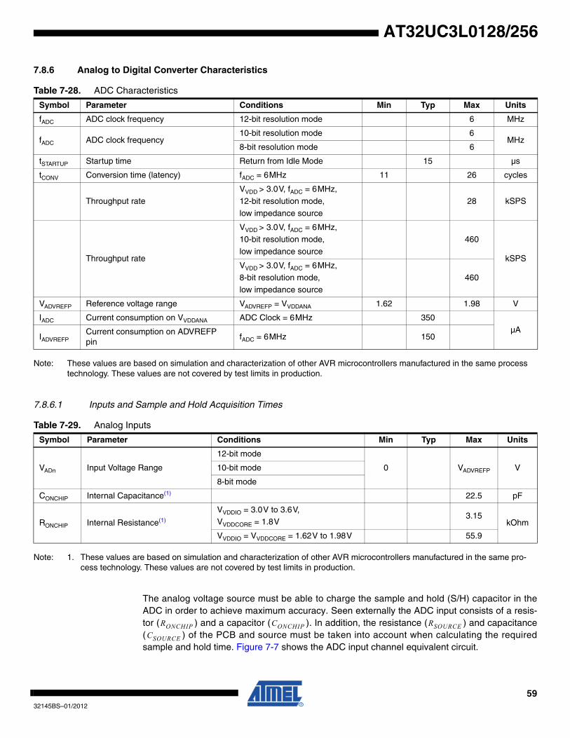
5932145BS–01/2012
AT32UC3L0128/256
7.8.6 Analog to Digital Converter Characteristics
Note: These values are based on simulation and characterization of other AVR microcontrollers manufactured in the same process technology. These values are not covered by test limits in production.
7.8.6.1 Inputs and Sample and Hold Acquisition Times
Note: 1. These values are based on simulation and characterization of other AVR microcontrollers manufactured in the same pro-cess technology. These values are not covered by test limits in production.
The analog voltage source must be able to charge the sample and hold (S/H) capacitor in theADC in order to achieve maximum accuracy. Seen externally the ADC input consists of a resis-tor ( ) and a capacitor ( ). In addition, the resistance ( ) and capacitance( ) of the PCB and source must be taken into account when calculating the requiredsample and hold time. Figure 7-7 shows the ADC input channel equivalent circuit.
Table 7-28. ADC Characteristics
Symbol Parameter Conditions Min Typ Max Units
fADC ADC clock frequency 12-bit resolution mode 6 MHz
fADC ADC clock frequency10-bit resolution mode 6
MHz8-bit resolution mode 6
tSTARTUP Startup time Return from Idle Mode 15 µs
tCONV Conversion time (latency) fADC = 6MHz 11 26 cycles
Throughput rate
VVDD > 3.0V, fADC = 6MHz,
12-bit resolution mode,
low impedance source
28 kSPS
Throughput rate
VVDD > 3.0V, fADC = 6MHz, 10-bit resolution mode,
low impedance source
460
kSPSVVDD > 3.0V, fADC = 6MHz,
8-bit resolution mode,low impedance source
460
VADVREFP Reference voltage range VADVREFP = VVDDANA 1.62 1.98 V
IADC Current consumption on VVDDANA ADC Clock = 6MHz 350
µAIADVREFP
Current consumption on ADVREFP pin
fADC = 6MHz 150
Table 7-29. Analog Inputs
Symbol Parameter Conditions Min Typ Max Units
VADn Input Voltage Range
12-bit mode
0 VADVREFP V10-bit mode
8-bit mode
CONCHIP Internal Capacitance(1) 22.5 pF
RONCHIP Internal Resistance(1)
VVDDIO = 3.0V to 3.6V, VVDDCORE = 1.8V
3.15kOhm
VVDDIO = VVDDCORE = 1.62V to 1.98V 55.9
RONCHIP CONCHIP RSOURCECSOURCE

6032145BS–01/2012
AT32UC3L0128/256
Figure 7-7. ADC Input
The minimum sample and hold time (in ns) can be found using this formula:
Where n is the number of bits in the conversion. is defined by the SHTIM field in theADCIFB ACR register. Please refer to the ADCIFB chapter for more information.
7.8.6.2 Applicable Conditions and Derating Data
Note: 1. These values are based on simulation and characterization of other AVR microcontrollers manufactured in the same pro-cess technology. These values are not covered by test limits in production.
ADCVREFP/2
CONCHIP
RONCHIPPositive InputRSOURCE
CSOURCEVIN
tSAMPLEHOLD RONCHIP RSOURCE+( ) CONCHIP CSOURCE+( )× 2n 1+( )ln×≥
tSAMPLEHOLD
Table 7-30. Transfer Characteristics 12-bit Resolution Mode(1)
Parameter Conditions Min Typ Max Units
Resolution 12 Bit
Integral non-linearity
ADC clock frequency = 6MHz,
Input Voltage Range = 0 - VADVREFP+/-4
LSB
ADC clock frequency = 6MHz, Input Voltage Range = (10% VADVREFP) - (90% VADVREFP)
+/-2
Differential non-linearity
ADC clock frequency = 6MHz
-1.5 1.5
Offset error +/-3
Gain error +/-5
Table 7-31. Transfer Characteristics, 10-bit Resolution Mode(1)
Parameter Conditions Min Typ Max Units
Resolution 10 Bit
Integral non-linearity
ADC clock frequency = 6MHz
+/-1
LSBDifferential non-linearity -1 1
Offset error +/-1
Gain error +/-2
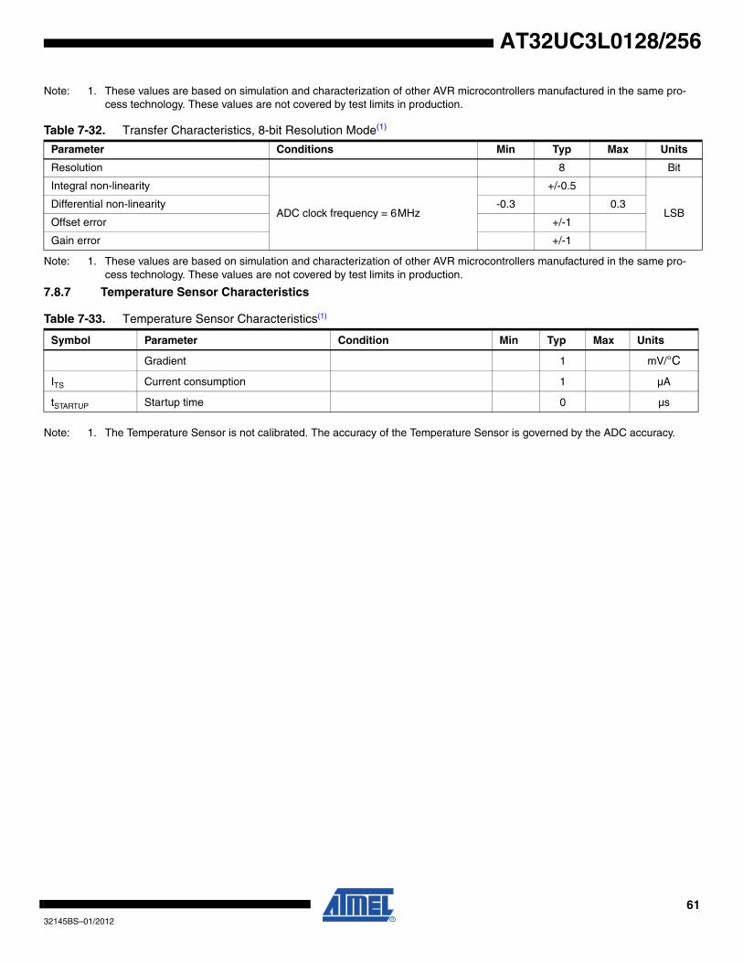
6132145BS–01/2012
AT32UC3L0128/256
Note: 1. These values are based on simulation and characterization of other AVR microcontrollers manufactured in the same pro-cess technology. These values are not covered by test limits in production.
Note: 1. These values are based on simulation and characterization of other AVR microcontrollers manufactured in the same pro-cess technology. These values are not covered by test limits in production.
7.8.7 Temperature Sensor Characteristics
Note: 1. The Temperature Sensor is not calibrated. The accuracy of the Temperature Sensor is governed by the ADC accuracy.
Table 7-32. Transfer Characteristics, 8-bit Resolution Mode(1)
Parameter Conditions Min Typ Max Units
Resolution 8 Bit
Integral non-linearity
ADC clock frequency = 6MHz
+/-0.5
LSBDifferential non-linearity -0.3 0.3
Offset error +/-1
Gain error +/-1
Table 7-33. Temperature Sensor Characteristics(1)
Symbol Parameter Condition Min Typ Max Units
Gradient 1 mV/°C
ITS Current consumption 1 µA
tSTARTUP Startup time 0 µs

6232145BS–01/2012
AT32UC3L0128/256
7.8.8 Analog Comparator Characteristics
Notes: 1. AC.CONFn.FLEN and AC.CONFn.HYS fields, refer to the Analog Comparator Interface chapter. 2. Referring to fAC.3. These values are based on simulation and characterization of other AVR microcontrollers manufactured in the same pro-
cess technology. These values are not covered by test limits in production.
7.8.9 Capacitive Touch Characteristics
7.8.9.1 Discharge Current Source
Note: 1. These values are based on simulation and characterization of other AVR microcontrollers manufactured in the same pro-cess technology. These values are not covered by test limits in production.
Table 7-34. Analog Comparator Characteristics
Symbol Parameter Condition Min Typ Max Units
Positive input voltage range(3) -0.2 VVDDIO + 0.3
VNegative input voltage range(3) -0.2 VVDDIO - 0.6
Statistical offset(3)
VACREFN = 1.0V,
fAC = 12MHz, filter length = 2, hysteresis = 0(1)
20 mV
fACClock frequency for GCLK4(3) 12 MHz
Throughput rate(3) fAC = 12MHz 12 000 000Comparisons per second
Propagation delay
Delay from input change to Interrupt Status Register Changes
ns
IACCurrent consumption(3)
All channels, VDDIO = 3.3V,
fA = 3MHz420 µA
tSTARTUP Startup time 3 cycles
Input current per pin(3) 0.2 µA/MHz(2)
Table 7-35. DICS Characteristics
Symbol Parameter Min Typ Max Unit
RREF Internal resistor 170 kOhm
k Trim step size(1) 0.7 %
1tCLKACIFB fAC×---------------------------------------- 3+⎝ ⎠
⎛ ⎞ tCLKACIFB×

6332145BS–01/2012
AT32UC3L0128/256
7.8.9.2 Strong Pull-up Pull-down
Table 7-36. Strong Pull-up Pull-down
Parameter Min Typ Max Unit
Pull-down resistor 1kOhm
Pull-up resistor 1

6432145BS–01/2012
AT32UC3L0128/256
7.9 Timing Characteristics
7.9.1 Startup, Reset, and Wake-up Timing
The startup, reset, and wake-up timings are calculated using the following formula:
Where and are found in Table 7-37. is the period of the CPU clock. If aclock source other than RCSYS is selected as the CPU clock, the oscillator startup time,
, must be added to the wake-up time from the stop, deepstop, and static sleepmodes. Please refer to the source for the CPU clock in the ”Oscillator Characteristics” on page49 for more details about oscillator startup times.
Note: 1. These values are based on simulation and characterization of other AVR microcontrollers manufactured in the same pro-cess technology. These values are not covered by test limits in production.
7.9.2 RESET_N Timing
Note: 1. These values are based on simulation and characterization of other AVR microcontrollers manufactured in the same pro-cess technology. These values are not covered by test limits in production.
t tCONST NCPU tCPU×+=
tCONST NCPU tCPU
tOSCSTART
Table 7-37. Maximum Reset and Wake-up Timing(1)
Parameter Measuring Max (in µs) Max
Startup time from power-up, using regulator
Time from VDDIN crossing the VPOT+ threshold of POR33 to the first instruction entering the decode stage of CPU. VDDCORE is supplied by the internal regulator.
2210 0
Startup time from power-up, no regulator
Time from VDDIN crossing the VPOT+ threshold of POR33 to the first instruction entering the decode stage of CPU. VDDCORE is connected to VDDIN.
1810 0
Startup time from reset releaseTime from releasing a reset source (except POR18, POR33, and SM33) to the first instruction entering the decode stage of CPU.
170 0
Wake-up
Idle
From wake-up event to the first instruction of an interrupt routine entering the decode stage of the CPU.
0 19
Frozen 0 110
Standby 0 110
Stop 27 + 116
Deepstop 27 + 116
Static 97 + 116
Wake-up from shutdownFrom wake-up event to the first instruction entering the decode stage of the CPU.
1180 0
tCONST NCPU
tOSCSTARTtOSCSTARTtOSCSTART
Table 7-38. RESET_N Waveform Parameters(1)
Symbol Parameter Conditions Min Max Units
tRESET RESET_N minimum pulse length 10 ns

6532145BS–01/2012
AT32UC3L0128/256
7.9.3 USART in SPI Mode Timing
7.9.3.1 Master mode
Figure 7-8. USART in SPI Master Mode with (CPOL= CPHA= 0) or (CPOL= CPHA= 1)
Figure 7-9. USART in SPI Master Mode with (CPOL= 0 and CPHA= 1) or (CPOL= 1 and CPHA= 0)
Notes: 1. These values are based on simulation and characterization of other AVR microcontrollers manufactured in the same pro-cess technology. These values are not covered by test limits in production.
2. Where:
USPI0 USPI1
MISO
SPCK
MOSI
USPI2
USPI3 USPI4
MISO
SPCK
MOSI
USPI5
Table 7-39. USART in SPI Mode Timing, Master Mode(1)
Symbol Parameter Conditions Min Max Units
USPI0 MISO setup time before SPCK rises
VVDDIO from 3.0V to 3.6V,
maximum external
capacitor = 40pF
28.7 + tSAMPLE(2)
ns
USPI1 MISO hold time after SPCK rises 0
USPI2 SPCK rising to MOSI delay 16.5
USPI3 MISO setup time before SPCK falls 25.8 + tSAMPLE(2)
USPI4 MISO hold time after SPCK falls 0
USPI5 SPCK falling to MOSI delay 21.19
tSAMPLE tSPCKtSPCK
2 tCLKUSART×------------------------------------
12---⎝ ⎠
⎛ ⎞ tCLKUSART×–=
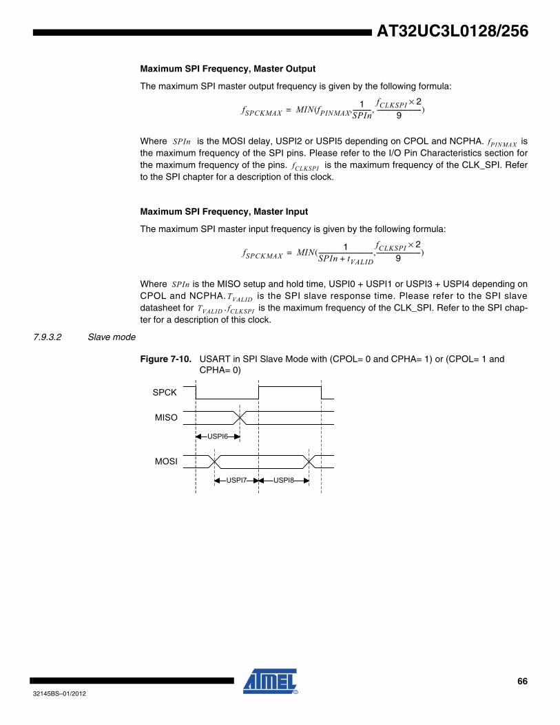
6632145BS–01/2012
AT32UC3L0128/256
Maximum SPI Frequency, Master Output
The maximum SPI master output frequency is given by the following formula:
Where is the MOSI delay, USPI2 or USPI5 depending on CPOL and NCPHA. isthe maximum frequency of the SPI pins. Please refer to the I/O Pin Characteristics section forthe maximum frequency of the pins. is the maximum frequency of the CLK_SPI. Referto the SPI chapter for a description of this clock.
Maximum SPI Frequency, Master Input
The maximum SPI master input frequency is given by the following formula:
Where is the MISO setup and hold time, USPI0 + USPI1 or USPI3 + USPI4 depending onCPOL and NCPHA. is the SPI slave response time. Please refer to the SPI slavedatasheet for . is the maximum frequency of the CLK_SPI. Refer to the SPI chap-ter for a description of this clock.
7.9.3.2 Slave mode
Figure 7-10. USART in SPI Slave Mode with (CPOL= 0 and CPHA= 1) or (CPOL= 1 and CPHA= 0)
fSPCKMAX MIN fPINMAX1
SPIn------------
fCLKSPI 2×9
-----------------------------,( , )=
SPIn fPINMAX
fCLKSPI
fSPCKMAX MIN 1SPIn tVALID+------------------------------------
fCLKSPI 2×9
-----------------------------( , )=
SPInTVALID
TVALID fCLKSPI
USPI7 USPI8
MISO
SPCK
MOSI
USPI6

6732145BS–01/2012
AT32UC3L0128/256
Figure 7-11. USART in SPI Slave Mode with (CPOL= CPHA= 0) or (CPOL= CPHA= 1)
Figure 7-12. USART in SPI Slave Mode, NPCS Timing
Notes: 1. These values are based on simulation and characterization of other AVR microcontrollers manufactured in the same pro-cess technology. These values are not covered by test limits in production.
2. Where:
USPI10 USPI11
MISO
SPCK
MOSI
USPI9
USPI14
USPI12
USPI15
USPI13
NSS
SPCK, CPOL=0
SPCK, CPOL=1
Table 7-40. USART in SPI mode Timing, Slave Mode(1)
Symbol Parameter Conditions Min Max Units
USPI6 SPCK falling to MISO delay
VVDDIO from 3.0V to 3.6V,
maximum external
capacitor = 40pF
37.3
ns
USPI7 MOSI setup time before SPCK rises2.6 + tSAMPLE
(2) + tCLK_USART
USPI8 MOSI hold time after SPCK rises 0
USPI9 SPCK rising to MISO delay 37.0
USPI10 MOSI setup time before SPCK falls2.6 + tSAMPLE
(2) + tCLK_USART
USPI11 MOSI hold time after SPCK falls 0
USPI12 NSS setup time before SPCK rises 27.2
USPI13 NSS hold time after SPCK falls 0
USPI14 NSS setup time before SPCK falls 27.2
USPI15 NSS hold time after SPCK rises 0
tSAMPLE tSPCKtSPCK
2 tCLKUSART×------------------------------------
12---+⎝ ⎠
⎛ ⎞ tCLKUSART×–=

6832145BS–01/2012
AT32UC3L0128/256
Maximum SPI Frequency, Slave Input Mode
The maximum SPI slave input frequency is given by the following formula:
Where is the MOSI setup and hold time, USPI7 + USPI8 or USPI10 + USPI11 dependingon CPOL and NCPHA. is the maximum frequency of the CLK_SPI. Refer to the SPIchapter for a description of this clock.
Maximum SPI Frequency, Slave Output Mode
The maximum SPI slave output frequency is given by the following formula:
Where is the MISO delay, USPI6 or USPI9 depending on CPOL and NCPHA. isthe SPI master setup time. Please refer to the SPI master datasheet for . is themaximum frequency of the CLK_SPI. Refer to the SPI chapter for a description of thisclock. is the maximum frequency of the SPI pins. Please refer to the I/O Pin Characteris-tics section for the maximum frequency of the pins.
7.9.4 SPI Timing
7.9.4.1 Master mode
Figure 7-13. SPI Master Mode with (CPOL= NCPHA= 0) or (CPOL= NCPHA= 1)
fSPCKMAX MINfCLKSPI 2×
9-----------------------------
1SPIn------------( , )=
SPInfCLKSPI
fSPCKMAX MINfCLKSPI 2×
9----------------------------- fPINMAX, 1
SPIn tSETUP+------------------------------------( , )=
SPIn TSETUPTSETUP fCLKSPI
fPINMAX
SPI0 SPI1
MISO
SPCK
MOSI
SPI2

6932145BS–01/2012
AT32UC3L0128/256
Figure 7-14. SPI Master Mode with (CPOL= 0 and NCPHA= 1) or (CPOL= 1 and NCPHA= 0)
Note: 1. These values are based on simulation and characterization of other AVR microcontrollers manufactured in the same pro-cess technology. These values are not covered by test limits in production.
Maximum SPI Frequency, Master Output
The maximum SPI master output frequency is given by the following formula:
Where is the MOSI delay, SPI2 or SPI5 depending on CPOL and NCPHA. is themaximum frequency of the SPI pins. Please refer to the I/O Pin Characteristics section for themaximum frequency of the pins.
Maximum SPI Frequency, Master Input
The maximum SPI master input frequency is given by the following formula:
Where is the MISO setup and hold time, SPI0 + SPI1 or SPI3 + SPI4 depending onCPOL and NCPHA. is the SPI slave response time. Please refer to the SPI slavedatasheet for .
SPI3 SPI4
MISO
SPCK
MOSI
SPI5
Table 7-41. SPI Timing, Master Mode(1)
Symbol Parameter Conditions Min Max Units
SPI0 MISO setup time before SPCK rises
VVDDIO from 3.0V to 3.6V,
maximum external
capacitor = 40pF
33.4 + (tCLK_SPI)/2
ns
SPI1 MISO hold time after SPCK rises 0
SPI2 SPCK rising to MOSI delay 7.1
SPI3 MISO setup time before SPCK falls 29.2 + (tCLK_SPI)/2
SPI4 MISO hold time after SPCK falls 0
SPI5 SPCK falling to MOSI delay 8.63
fSPCKMAX MIN fPINMAX1
SPIn------------( , )=
SPIn fPINMAX
fSPCKMAX1
SPIn tVALID+------------------------------------=
SPIntVALID
tVALID

7032145BS–01/2012
AT32UC3L0128/256
7.9.4.2 Slave mode
Figure 7-15. SPI Slave Mode with (CPOL= 0 and NCPHA= 1) or (CPOL= 1 and NCPHA= 0)
Figure 7-16. SPI Slave Mode with (CPOL= NCPHA= 0) or (CPOL= NCPHA= 1)
Figure 7-17. SPI Slave Mode, NPCS Timing
SPI7 SPI8
MISO
SPCK
MOSI
SPI6
SPI10 SPI11
MISO
SPCK
MOSI
SPI9
SPI14
SPI12
SPI15
SPI13
NPCS
SPCK, CPOL=0
SPCK, CPOL=1

7132145BS–01/2012
AT32UC3L0128/256
Note: 1. These values are based on simulation and characterization of other AVR microcontrollers manufactured in the same pro-cess technology. These values are not covered by test limits in production.
Maximum SPI Frequency, Slave Input Mode
The maximum SPI slave input frequency is given by the following formula:
Where is the MOSI setup and hold time, SPI7 + SPI8 or SPI10 + SPI11 depending onCPOL and NCPHA. is the maximum frequency of the CLK_SPI. Refer to the SPI chap-ter for a description of this clock.
Maximum SPI Frequency, Slave Output Mode
The maximum SPI slave output frequency is given by the following formula:
Where is the MISO delay, SPI6 or SPI9 depending on CPOL and NCPHA. is theSPI master setup time. Please refer to the SPI master datasheet for . is the max-imum frequency of the SPI pins. Please refer to the I/O Pin Characteristics section for themaximum frequency of the pins.
7.9.5 TWIM/TWIS Timing
Figure 7-43 shows the TWI-bus timing requirements and the compliance of the device withthem. Some of these requirements (tr and tf) are met by the device without requiring user inter-vention. Compliance with the other requirements (tHD-STA, tSU-STA, tSU-STO, tHD-DAT, tSU-DAT-TWI, tLOW-
TWI, tHIGH, and fTWCK) requires user intervention through appropriate programming of the relevant
Table 7-42. SPI Timing, Slave Mode(1)
Symbol Parameter Conditions Min Max Units
SPI6 SPCK falling to MISO delay
VVDDIO from 3.0V to 3.6V,
maximum external
capacitor = 40pF
29.4
ns
SPI7 MOSI setup time before SPCK rises 0
SPI8 MOSI hold time after SPCK rises 6.0
SPI9 SPCK rising to MISO delay 29.0
SPI10 MOSI setup time before SPCK falls 0
SPI11 MOSI hold time after SPCK falls 5.5
SPI12 NPCS setup time before SPCK rises 3.4
SPI13 NPCS hold time after SPCK falls 1.1
SPI14 NPCS setup time before SPCK falls 3.3
SPI15 NPCS hold time after SPCK rises 0.7
fSPCKMAX MIN fCLKSPI1
SPIn------------( , )=
SPInfCLKSPI
fSPCKMAX MIN fPINMAX1
SPIn tSETUP+------------------------------------( , )=
SPIn tSETUPtSETUP fPINMAX
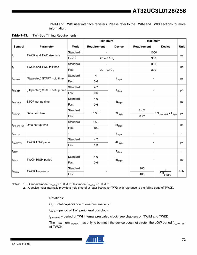
7232145BS–01/2012
AT32UC3L0128/256
TWIM and TWIS user interface registers. Please refer to the TWIM and TWIS sections for moreinformation.
Notes: 1. Standard mode: ; fast mode: .2. A device must internally provide a hold time of at least 300 ns for TWD with reference to the falling edge of TWCK.
Notations:
Cb = total capacitance of one bus line in pF
tclkpb = period of TWI peripheral bus clock
tprescaled = period of TWI internal prescaled clock (see chapters on TWIM and TWIS)
The maximum tHD;DAT has only to be met if the device does not stretch the LOW period (tLOW-TWI)of TWCK.
Table 7-43. TWI-Bus Timing Requirements
Symbol Parameter Mode
Minimum Maximum
UnitRequirement Device Requirement Device
tr TWCK and TWD rise timeStandard(1) - 1000
nsFast(1) 20 + 0.1Cb 300
tf TWCK and TWD fall timeStandard - 300
nsFast 20 + 0.1Cb 300
tHD-STA (Repeated) START hold timeStandard 4
tclkpb - μsFast 0.6
tSU-STA (Repeated) START set-up timeStandard 4.7
tclkpb - μsFast 0.6
tSU-STO STOP set-up timeStandard 4.0
4tclkpb - μsFast 0.6
tHD-DAT Data hold timeStandard
0.3(2) 2tclkpb
3.45()
15tprescaled + tclkpb μsFast 0.9()
tSU-DAT-TWI Data set-up timeStandard 250
2tclkpb - nsFast 100
tSU-DAT - - tclkpb - -
tLOW-TWI TWCK LOW periodStandard 4.7
4tclkpb - μsFast 1.3
tLOW - - tclkpb - -
tHIGH TWCK HIGH periodStandard 4.0
8tclkpb - μsFast 0.6
fTWCK TWCK frequencyStandard
-100
kHzFast 400
112tclkpb------------------------
fTWCK 100 kHz≤ fTWCK 100 kHz>

7332145BS–01/2012
AT32UC3L0128/256
7.9.6 JTAG Timing
Figure 7-18. JTAG Interface Signals
Note: 1. These values are based on simulation and characterization of other AVR microcontrollers manufactured in the same pro-cess technology. These values are not covered by test limits in production.
JTAG2
JTAG3
JTAG1
JTAG4
JTAG0
TMS/TDI
TCK
TDO
JTAG5
JTAG6
JTAG7 JTAG8
JTAG9
JTAG10
BoundaryScan Inputs
BoundaryScan Outputs
Table 7-44. JTAG Timings(1)
Symbol Parameter Conditions Min Max Units
JTAG0 TCK Low Half-period
VVDDIO from 3.0V to 3.6V,
maximum external
capacitor = 40pF
21.8
ns
JTAG1 TCK High Half-period 8.6
JTAG2 TCK Period 30.3
JTAG3 TDI, TMS Setup before TCK High 2.0
JTAG4 TDI, TMS Hold after TCK High 2.3
JTAG5 TDO Hold Time 9.5
JTAG6 TCK Low to TDO Valid 21.8
JTAG7 Boundary Scan Inputs Setup Time 0.6
JTAG8 Boundary Scan Inputs Hold Time 6.9
JTAG9 Boundary Scan Outputs Hold Time 9.3
JTAG10 TCK to Boundary Scan Outputs Valid 32.2

7432145BS–01/2012
AT32UC3L0128/256
8. Mechanical Characteristics
8.1 Thermal Considerations
8.1.1 Thermal DataTable 8-1 summarizes the thermal resistance data depending on the package.
8.1.2 Junction TemperatureThe average chip-junction temperature, TJ, in °C can be obtained from the following:
1.
2.
where:
• θJA = package thermal resistance, Junction-to-ambient (°C/W), provided in Table 8-1.
• θJC = package thermal resistance, Junction-to-case thermal resistance (°C/W), provided in Table 8-1.
• θHEAT SINK = cooling device thermal resistance (°C/W), provided in the device datasheet.
• PD = device power consumption (W) estimated from data provided in Section 7.4 on page 42.
• TA = ambient temperature (°C).
From the first equation, the user can derive the estimated lifetime of the chip and decide if acooling device is necessary or not. If a cooling device is to be fitted on the chip, the secondequation should be used to compute the resulting average chip-junction temperature TJ in °C.
Table 8-1. Thermal Resistance Data
Symbol Parameter Condition Package Typ Unit
θJA Junction-to-ambient thermal resistance Still Air TQFP48 54.4°C/W
θJC Junction-to-case thermal resistance TQFP48 15.7
θJA Junction-to-ambient thermal resistance Still Air QFN48 26.0°C/W
θJC Junction-to-case thermal resistance QFN48 1.6
θJA Junction-to-ambient thermal resistance Still Air TLLGA48 25.4°C/W
θJC Junction-to-case thermal resistance TLLGA48 12.7
TJ TA PD θJA×( )+=
TJ TA P( D θ( HEATSINK× θJC ) )+ +=

7532145BS–01/2012
AT32UC3L0128/256
8.2 Package Drawings
Figure 8-1. TQFP-48 Package Drawing
Table 8-2. Device and Package Maximum Weight
140 mg
Table 8-3. Package Characteristics
Moisture Sensitivity Level MSL3
Table 8-4. Package Reference
JEDEC Drawing Reference MS-026
JESD97 Classification E3

7632145BS–01/2012
AT32UC3L0128/256
Figure 8-2. QFN-48 Package Drawing
Note: The exposed pad is not connected to anything internally, but should be soldered to ground to increase board level reliability.
Table 8-5. Device and Package Maximum Weight
140 mg
Table 8-6. Package Characteristics
Moisture Sensitivity Level MSL3
Table 8-7. Package Reference
JEDEC Drawing Reference M0-220
JESD97 Classification E3

7732145BS–01/2012
AT32UC3L0128/256
Figure 8-3. TLLGA-48 Package Drawing
Table 8-8. Device and Package Maximum Weight
39.3 mg
Table 8-9. Package Characteristics
Moisture Sensitivity Level MSL3
Table 8-10. Package Reference
JEDEC Drawing Reference N/A
JESD97 Classification E4

7832145BS–01/2012
AT32UC3L0128/256
8.3 Soldering ProfileTable 8-11 gives the recommended soldering profile from J-STD-20.
A maximum of three reflow passes is allowed per component.
Table 8-11. Soldering Profile
Profile Feature Green Package
Average Ramp-up Rate (217°C to Peak) 3°C/s max
Preheat Temperature 175°C ±25°C 150-200°C
Time Maintained Above 217°C 60-150 s
Time within 5°C of Actual Peak Temperature 30 s
Peak Temperature Range 260°C
Ramp-down Rate 6°C/s max
Time 25°C to Peak Temperature 8 minutes max

7932145BS–01/2012
AT32UC3L0128/256
9. Ordering Information
Table 9-1. Ordering Information
Device Ordering Code Carrier Type Package Package TypeTemperature Operating Range
AT32UC3L0256
AT32UC3L0256-AUTES ES
TQFP 48
JESD97 Classification E3
Industrial (-40°C to 85°C)
AT32UC3L0256-AUT Tray
AT32UC3L0256-AUR Tape & Reel
AT32UC3L0256-ZAUTES ES
QFN 48AT32UC3L0256-ZAUT Tray
AT32UC3L0256-ZAUR Tape & Reel
AT32UC3L0256-D3HES ES
TLLGA 48 JESD97 Classification E4AT32UC3L0256-D3HT Tray
AT32UC3L0256-D3HR Tape & Reel
AT32UC3L0128
AT32UC3L0128-AUT TrayTQFP 48
JESD97 Classification E3AT32UC3L0128-AUR Tape & Reel
AT32UC3L0128-ZAUT TrayQFN 48
AT32UC3L0128-ZAUR Tape & Reel
AT32UC3L0128-D3HT TrayTLLGA 48 JESD97 Classification E4
AT32UC3L0128-D3HR Tape & Reel

8032145BS–01/2012
AT32UC3L0128/256
10. Errata
10.1 Rev. C
10.1.1 SCIF
1. The RC32K output on PA20 is not always permanently disabledThe RC32K output on PA20 may sometimes re-appear.Fix/WorkaroundBefore using RC32K for other purposes, the following procedure has to be followed in orderto properly disable it:- Run the CPU on RCSYS- Disable the output to PA20 by writing a zero to PM.PPCR.RC32OUT- Enable RC32K by writing a one to SCIF.RC32KCR.EN, and wait for this bit to be read asone- Disable RC32K by writing a zero to SCIF.RC32KCR.EN, and wait for this bit to be read aszero.
2. PLLCOUNT value larger than zero can cause PLLEN glitchInitializing the PLLCOUNT with a value greater than zero creates a glitch on the PLLEN sig-nal during asynchronous wake up.Fix/WorkaroundThe lock-masking mechanism for the PLL should not be used.The PLLCOUNT field of the PLL Control Register should always be written to zero.
3. Writing 0x5A5A5A5A to the SCIF memory range will enable the SCIF UNLOCK featureThe SCIF UNLOCK feature will be enabled if the value 0x5A5A5A5A is written to any loca-tion in the SCIF memory range.Fix/WorkaroundNone.
10.1.2 SPI
1. SPI data transfer hangs with CSR0.CSAAT==1 and MR.MODFDIS==0When CSR0.CSAAT==1 and mode fault detection is enabled (MR.MODFDIS==0), the SPImodule will not start a data transfer.Fix/WorkaroundDisable mode fault detection by writing a one to MR.MODFDIS.
2. Disabling SPI has no effect on the SR.TDRE bitDisabling SPI has no effect on the SR.TDRE bit whereas the write data command is filteredwhen SPI is disabled. Writing to TDR when SPI is disabled will not clear SR.TDRE. If SPI isdisabled during a PDCA transfer, the PDCA will continue to write data to TDR until its bufferis empty, and this data will be lost.Fix/WorkaroundDisable the PDCA, add two NOPs, and disable the SPI. To continue the transfer, enable theSPI and PDCA.
3. SPI disable does not work in SLAVE modeSPI disable does not work in SLAVE mode.Fix/WorkaroundRead the last received data, then perform a software reset by writing a one to the SoftwareReset bit in the Control Register (CR.SWRST).

8132145BS–01/2012
AT32UC3L0128/256
4. SPI bad serial clock generation on 2nd chip_select when SCBR=1, CPOL=1, andNCPHA=0When multiple chip selects (CS) are in use, if one of the baudrates equal 1 while one(CSRn.SCBR=1) of the others do not equal 1, and CSRn.CPOL=1 and CSRn.NCPHA=0,then an additional pulse will be generated on SCK.Fix/WorkaroundWhen multiple CS are in use, if one of the baudrates equals 1, the others must also equal 1if CSRn.CPOL=1 and CSRn.NCPHA=0.
5. SPI mode fault detection enable causes incorrect behaviorWhen mode fault detection is enabled (MR.MODFDIS==0), the SPI module may not operateproperly.Fix/WorkaroundAlways disable mode fault detection before using the SPI by writing a one to MR.MODFDIS.
6. SPI RDR.PCS is not correctThe PCS (Peripheral Chip Select) field in the SPI RDR (Receive Data Register) does notcorrectly indicate the value on the NPCS pins at the end of a transfer.Fix/WorkaroundDo not use the PCS field of the SPI RDR.
10.1.3 TWI
1. SMBALERT bit may be set after resetThe SMBus Alert (SMBALERT) bit in the Status Register (SR) might be erroneously set aftersystem reset.Fix/WorkaroundAfter system reset, clear the SR.SMBALERT bit before commencing any TWI transfer.
2. Clearing the NAK bit before the BTF bit is set locks up the TWI busWhen the TWIS is in transmit mode, clearing the NAK Received (NAK) bit of the Status Reg-ister (SR) before the end of the Acknowledge/Not Acknowledge cycle will cause the TWIS toattempt to continue transmitting data, thus locking up the bus.Fix/WorkaroundClear SR.NAK only after the Byte Transfer Finished (BTF) bit of the same register has beenset.
10.1.4 TC
1. Channel chaining skips first pulse for upper channelWhen chaining two channels using the Block Mode Register, the first pulse of the clockbetween the channels is skipped.Fix/WorkaroundConfigure the lower channel with RA = 0x1 and RC = 0x2 to produce a dummy clock cyclefor the upper channel. After the dummy cycle has been generated, indicated by theSR.CPCS bit, reconfigure the RA and RC registers for the lower channel with the realvalues.
10.1.5 CAT
1. CAT QMatrix sense capacitors discharged prematurelyAt the end of a QMatrix burst charging sequence that uses different burst count values fordifferent Y lines, the Y lines may be incorrectly grounded for up to n-1 periods of the periph-
8232145BS–01/2012
AT32UC3L0128/256
eral bus clock, where n is the ratio of the PB clock frequency to the GCLK_CAT frequency.This results in premature loss of charge from the sense capacitors and thus increased vari-ability of the acquired count values.Fix/WorkaroundEnable the 1kOhm drive resistors on all implemented QMatrix Y lines (CSA 1, 3, 5, 7, 9, 11,13, and/or 15) by writing ones to the corresponding odd bits of the CSARES register.
2. Autonomous CAT acquisition must be longer than AST source clock periodWhen using the AST to trigger CAT autonomous touch acquisition in sleep modes where theCAT bus clock is turned off, the CAT will start several acquisitions if the period of the ASTsource clock is larger than one CAT acquisition. One AST clock period after the AST trigger,the CAT clock will automatically stop and the CAT acquisition can be stopped prematurely,ruining the result.Fix/WorkaroundAlways ensure that the ATCFG1.max field is set so that the duration of the autonomoustouch acquisition is greater than one clock period of the AST source clock.
10.1.6 aWire
1. aWire MEMORY_SPEED_REQUEST command does not return correct CVThe aWire MEMORY_SPEED_REQUEST command does not return a CV corresponding tothe formula in the aWire Debug Interface chapter.Fix/WorkaroundI ssue a dummy read to add ress 0x100000000 be fo re i ssu ing theMEMORY_SPEED_REQUEST command and use this formula instead:
10.2 Rev. B
10.2.1 SCIF
1. The RC32K output on PA20 is not always permanently disabledThe RC32K output on PA20 may sometimes re-appear.Fix/WorkaroundBefore using RC32K for other purposes, the following procedure has to be followed in orderto properly disable it:- Run the CPU on RCSYS- Disable the output to PA20 by writing a zero to PM.PPCR.RC32OUT- Enable RC32K by writing a one to SCIF.RC32KCR.EN, and wait for this bit to be read asone- Disable RC32K by writing a zero to SCIF.RC32KCR.EN, and wait for this bit to be read aszero.
2. PLLCOUNT value larger than zero can cause PLLEN glitchInitializing the PLLCOUNT with a value greater than zero creates a glitch on the PLLEN sig-nal during asynchronous wake up.Fix/WorkaroundThe lock-masking mechanism for the PLL should not be used.The PLLCOUNT field of the PLL Control Register should always be written to zero.
3. Writing 0x5A5A5A5A to the SCIF memory range will enable the SCIF UNLOCK feature
fsab7fawCV 3–-----------------=

8332145BS–01/2012
AT32UC3L0128/256
The SCIF UNLOCK feature will be enabled if the value 0x5A5A5A5A is written to any loca-tion in the SCIF memory range.Fix/WorkaroundNone.
10.2.2 WDT
1. WDT Control Register does not have synchronization feedbackWhen writing to the Timeout Prescale Select (PSEL), Time Ban Prescale Select (TBAN),Enable (EN), or WDT Mode (MODE) fieldss of the WDT Control Register (CTRL), a synchro-nizer is started to propagate the values to the WDT clcok domain. This synchronizationtakes a finite amount of time, but only the status of the synchronization of the EN bit isreflected back to the user. Writing to the synchronized fields during synchronization can leadto undefined behavior. Fix/Workaround-When writing to the affected fields, the user must ensure a wait corresponding to 2 clockcycles of both the WDT peripheral bus clock and the selected WDT clock source.-When doing writes that changes the EN bit, the EN bit can be read back until it reflects thewritten value.
10.2.3 SPI
1. SPI data transfer hangs with CSR0.CSAAT==1 and MR.MODFDIS==0When CSR0.CSAAT==1 and mode fault detection is enabled (MR.MODFDIS==0), the SPImodule will not start a data transfer.Fix/WorkaroundDisable mode fault detection by writing a one to MR.MODFDIS.
2. Disabling SPI has no effect on the SR.TDRE bitDisabling SPI has no effect on the SR.TDRE bit whereas the write data command is filteredwhen SPI is disabled. Writing to TDR when SPI is disabled will not clear SR.TDRE. If SPI isdisabled during a PDCA transfer, the PDCA will continue to write data to TDR until its bufferis empty, and this data will be lost.Fix/WorkaroundDisable the PDCA, add two NOPs, and disable the SPI. To continue the transfer, enable theSPI and PDCA.
3. SPI disable does not work in SLAVE modeSPI disable does not work in SLAVE mode.Fix/WorkaroundRead the last received data, then perform a software reset by writing a one to the SoftwareReset bit in the Control Register (CR.SWRST).
4. SPI bad serial clock generation on 2nd chip_select when SCBR=1, CPOL=1, andNCPHA=0When multiple chip selects (CS) are in use, if one of the baudrates equal 1 while one(CSRn.SCBR=1) of the others do not equal 1, and CSRn.CPOL=1 and CSRn.NCPHA=0,then an additional pulse will be generated on SCK.Fix/WorkaroundWhen multiple CS are in use, if one of the baudrates equals 1, the others must also equal 1if CSRn.CPOL=1 and CSRn.NCPHA=0.
5. SPI mode fault detection enable causes incorrect behaviorWhen mode fault detection is enabled (MR.MODFDIS==0), the SPI module may not operate

8432145BS–01/2012
AT32UC3L0128/256
properly.Fix/WorkaroundAlways disable mode fault detection before using the SPI by writing a one to MR.MODFDIS.
6. SPI RDR.PCS is not correctThe PCS (Peripheral Chip Select) field in the SPI RDR (Receive Data Register) does notcorrectly indicate the value on the NPCS pins at the end of a transfer.Fix/WorkaroundDo not use the PCS field of the SPI RDR.
10.2.4 TWI
1. TWIS may not wake the device from sleep modeIf the CPU is put to a sleep mode (except Idle and Frozen) directly after a TWI Start condi-tion, the CPU may not wake upon a TWIS address match. The request is NACKed.Fix/WorkaroundWhen using the TWI address match to wake the device from sleep, do not switch to sleepmodes deeper than Frozen. Another solution is to enable asynchronous EIC wake on theTWIS clock (TWCK) or TWIS data (TWD) pins, in order to wake the system up on busevents.
2. SMBALERT bit may be set after resetThe SMBus Alert (SMBALERT) bit in the Status Register (SR) might be erroneously set aftersystem reset.Fix/WorkaroundAfter system reset, clear the SR.SMBALERT bit before commencing any TWI transfer.
3. Clearing the NAK bit before the BTF bit is set locks up the TWI busWhen the TWIS is in transmit mode, clearing the NAK Received (NAK) bit of the Status Reg-ister (SR) before the end of the Acknowledge/Not Acknowledge cycle will cause the TWIS toattempt to continue transmitting data, thus locking up the bus.Fix/WorkaroundClear SR.NAK only after the Byte Transfer Finished (BTF) bit of the same register has beenset.
10.2.5 PWMA
1. The SR.READY bit cannot be cleared by writing to SCR.READYThe Ready bit in the Status Register will not be cleared when writing a one to the corre-sponding bit in the Status Clear register. The Ready bit will be cleared when the Busy bit isset.Fix/WorkaroundDisable the Ready interrupt in the interrupt handler when receiving the interrupt. When anoperation that triggers the Busy/Ready bit is started, wait until the ready bit is low in the Sta-tus Register before enabling the interrupt.
10.2.6 TC
1. Channel chaining skips first pulse for upper channelWhen chaining two channels using the Block Mode Register, the first pulse of the clockbetween the channels is skipped.Fix/Workaround

8532145BS–01/2012
AT32UC3L0128/256
Configure the lower channel with RA = 0x1 and RC = 0x2 to produce a dummy clock cyclefor the upper channel. After the dummy cycle has been generated, indicated by theSR.CPCS bit, reconfigure the RA and RC registers for the lower channel with the realvalues.
10.2.7 CAT
1. CAT QMatrix sense capacitors discharged prematurelyAt the end of a QMatrix burst charging sequence that uses different burst count values fordifferent Y lines, the Y lines may be incorrectly grounded for up to n-1 periods of the periph-eral bus clock, where n is the ratio of the PB clock frequency to the GCLK_CAT frequency.This results in premature loss of charge from the sense capacitors and thus increased vari-ability of the acquired count values.Fix/WorkaroundEnable the 1kOhm drive resistors on all implemented QMatrix Y lines (CSA 1, 3, 5, 7, 9, 11,13, and/or 15) by writing ones to the corresponding odd bits of the CSARES register.
2. Autonomous CAT acquisition must be longer than AST source clock periodWhen using the AST to trigger CAT autonomous touch acquisition in sleep modes where theCAT bus clock is turned off, the CAT will start several acquisitions if the period of the ASTsource clock is larger than one CAT acquisition. One AST clock period after the AST trigger,the CAT clock will automatically stop and the CAT acquisition can be stopped prematurely,ruining the result.Fix/WorkaroundAlways ensure that the ATCFG1.max field is set so that the duration of the autonomoustouch acquisition is greater than one clock period of the AST source clock.
3. CAT consumes unnecessary power when disabled or when autonomous touch notusedA CAT prescaler controlled by the ATCFG0.DIV field will be active even when the CAT mod-ule is disabled or when the autonomous touch feature is not used, thereby causingunnecessary power consumption.Fix/WorkaroundIf the CAT module is not used, disable the CLK_CAT clock in the PM module. If the CATmodule is used but the autonomous touch feature is not used, the power consumption of theCAT module may be reduced by writing 0xFFFF to the ATCFG0.DIV field.
10.2.8 aWire
1. aWire MEMORY_SPEED_REQUEST command does not return correct CVThe aWire MEMORY_SPEED_REQUEST command does not return a CV corresponding tothe formula in the aWire Debug Interface chapter.Fix/WorkaroundI ssue a dummy read to add ress 0x100000000 be fo re i ssu ing theMEMORY_SPEED_REQUEST command and use this formula instead:
fsab7fawCV 3–-----------------=

8632145BS–01/2012
AT32UC3L0128/256
10.3 Rev. A
10.3.1 Device
1. JTAGID is wrongThe JTAGID is 0x021DF03F.Fix/WorkaroundNone.
10.3.2 FLASHCDW
1. General-purpose fuse programming does not workThe general-purpose fuses cannot be programmed and are stuck at 1. Please refer to theFuse Settings chapter in the FLASHCDW for more information about what functions areaffected.Fix/WorkaroundNone.
2. Set Security Bit command does not workThe Set Security Bit (SSB) command of the FLASHCDW does not work. The device cannotbe locked from external JTAG, aWire, or other debug accesses.Fix/WorkaroundNone.
3. Flash programming time is longer than specifiedThe flash programming time is now:
Fix/WorkaroundNone.
10.3.3 Power Manager
1. Clock Failure Detector (CFD) can be issued while turning off the CFDWhile turning off the CFD, the CFD bit in the Status Register (SR) can be set. This willchange the main clock source to RCSYS.Fix/WorkaroundSolution 1: Enable CFD interrupt. If CFD interrupt is issues after turning off the CFD, switchback to original main clock source.Solution 2: Only turn off the CFD while running the main clock on RCSYS.
2. Sleepwalking in idle and frozen sleep mode will mask all other PB clocks
Table 10-1. Flash Characteristics
Symbol Parameter Conditions Min Typ Max Unit
TFPP Page programming time
fCLK_HSB= 50MHz
7.5
ms
TFPE Page erase time 7.5
TFFP Fuse programming time 1
TFEA Full chip erase time (EA) 9
TFCEJTAG chip erase time (CHIP_ERASE)
fCLK_HSB= 115kHz 250

8732145BS–01/2012
AT32UC3L0128/256
If the CPU is in idle or frozen sleep mode and a module is in a state that triggers sleep walk-ing, all PB clocks will be masked except the PB clock to the sleepwalking module.Fix/WorkaroundMask all clock requests in the PM.PPCR register before going into idle or frozen mode.
2. Unused PB clocks are runningThree unused PBA clocks are enabled by default and will cause increased active powerconsumption.Fix/WorkaroundDisable the clocks by writing zeroes to bits [27:25] in the PBA clock mask register.
10.3.4 SCIF
1. The RC32K output on PA20 is not always permanently disabledThe RC32K output on PA20 may sometimes re-appear.Fix/WorkaroundBefore using RC32K for other purposes, the following procedure has to be followed in orderto properly disable it:- Run the CPU on RCSYS- Disable the output to PA20 by writing a zero to PM.PPCR.RC32OUT- Enable RC32K by writing a one to SCIF.RC32KCR.EN, and wait for this bit to be read asone- Disable RC32K by writing a zero to SCIF.RC32KCR.EN, and wait for this bit to be read aszero.
2. PLL lock might not clear after disableUnder certain circumstances, the lock signal from the Phase Locked Loop (PLL) oscillatormay not go back to zero after the PLL oscillator has been disabled. This can cause the prop-agation of clock signals with the wrong frequency to parts of the system that use the PLLclock.Fix/WorkaroundPLL must be turned off before entering STOP, DEEPSTOP or STATIC sleep modes. If PLLhas been turned off, a delay of 30us must be observed after the PLL has been enabledagain before the SCIF.PLL0LOCK bit can be used as a valid indication that the PLL islocked.
3. PLLCOUNT value larger than zero can cause PLLEN glitchInitializing the PLLCOUNT with a value greater than zero creates a glitch on the PLLEN sig-nal during asynchronous wake up.Fix/WorkaroundThe lock-masking mechanism for the PLL should not be used.The PLLCOUNT field of the PLL Control Register should always be written to zero.
4. RCSYS is not calibratedThe RCSYS is not calibrated and will run faster than 115.2kHz. Frequencies around 150kHzcan be expected.Fix/WorkaroundIf a known clock source is available the RCSYS can be runtime calibrated by using the fre-quency meter (FREQM) and tuning the RCSYS by writing to the RCCR register in SCIF.
5. Writing 0x5A5A5A5A to the SCIF memory range will enable the SCIF UNLOCK featureThe SCIF UNLOCK feature will be enabled if the value 0x5A5A5A5A is written to any loca-tion in the SCIF memory range.Fix/Workaround

8832145BS–01/2012
AT32UC3L0128/256
None.
10.3.5 WDT
1. Clearing the Watchdog Timer (WDT) counter in second half of timeout period willissue a Watchdog resetIf the WDT counter is cleared in the second half of the timeout period, the WDT will immedi-ately issue a Watchdog reset.Fix/WorkaroundUse twice as long timeout period as needed and clear the WDT counter within the first halfof the timeout period. If the WDT counter is cleared after the first half of the timeout period,you will get a Watchdog reset immediately. If the WDT counter is not cleared at all, the timebefore the reset will be twice as long as needed.
2. WDT Control Register does not have synchronization feedbackWhen writing to the Timeout Prescale Select (PSEL), Time Ban Prescale Select (TBAN),Enable (EN), or WDT Mode (MODE) fieldss of the WDT Control Register (CTRL), a synchro-nizer is started to propagate the values to the WDT clcok domain. This synchronizationtakes a finite amount of time, but only the status of the synchronization of the EN bit isreflected back to the user. Writing to the synchronized fields during synchronization can leadto undefined behavior. Fix/Workaround-When writing to the affected fields, the user must ensure a wait corresponding to 2 clockcycles of both the WDT peripheral bus clock and the selected WDT clock source.-When doing writes that changes the EN bit, the EN bit can be read back until it reflects thewritten value.
10.3.6 GPIO
1. Clearing Interrupt flags can mask other interruptsWhen clearing interrupt flags in a GPIO port, interrupts on other pins of that port, happeningin the same clock cycle will not be registered.Fix/WorkaroundRead the PVR register of the port before and after clearing the interrupt to see if any pinchange has happened while clearing the interrupt. If any change occurred in the PVRbetween the reads, they must be treated as an interrupt.
10.3.7 SPI
1. SPI data transfer hangs with CSR0.CSAAT==1 and MR.MODFDIS==0When CSR0.CSAAT==1 and mode fault detection is enabled (MR.MODFDIS==0), the SPImodule will not start a data transfer.Fix/WorkaroundDisable mode fault detection by writing a one to MR.MODFDIS.
2. Disabling SPI has no effect on the SR.TDRE bitDisabling SPI has no effect on the SR.TDRE bit whereas the write data command is filteredwhen SPI is disabled. Writing to TDR when SPI is disabled will not clear SR.TDRE. If SPI isdisabled during a PDCA transfer, the PDCA will continue to write data to TDR until its bufferis empty, and this data will be lost.Fix/WorkaroundDisable the PDCA, add two NOPs, and disable the SPI. To continue the transfer, enable theSPI and PDCA.

8932145BS–01/2012
AT32UC3L0128/256
3. SPI disable does not work in SLAVE modeSPI disable does not work in SLAVE mode.Fix/WorkaroundRead the last received data, then perform a software reset by writing a one to the SoftwareReset bit in the Control Register (CR.SWRST).
4. SPI bad serial clock generation on 2nd chip_select when SCBR=1, CPOL=1, andNCPHA=0When multiple chip selects (CS) are in use, if one of the baudrates equal 1 while one(CSRn.SCBR=1) of the others do not equal 1, and CSRn.CPOL=1 and CSRn.NCPHA=0,then an additional pulse will be generated on SCK.Fix/WorkaroundWhen multiple CS are in use, if one of the baudrates equals 1, the others must also equal 1if CSRn.CPOL=1 and CSRn.NCPHA=0.
5. SPI mode fault detection enable causes incorrect behaviorWhen mode fault detection is enabled (MR.MODFDIS==0), the SPI module may not operateproperly.Fix/WorkaroundAlways disable mode fault detection before using the SPI by writing a one to MR.MODFDIS.
6. SPI RDR.PCS is not correctThe PCS (Peripheral Chip Select) field in the SPI RDR (Receive Data Register) does notcorrectly indicate the value on the NPCS pins at the end of a transfer.Fix/WorkaroundDo not use the PCS field of the SPI RDR.
10.3.8 TWI
1. TWIS may not wake the device from sleep modeIf the CPU is put to a sleep mode (except Idle and Frozen) directly after a TWI Start condi-tion, the CPU may not wake upon a TWIS address match. The request is NACKed.Fix/WorkaroundWhen using the TWI address match to wake the device from sleep, do not switch to sleepmodes deeper than Frozen. Another solution is to enable asynchronous EIC wake on theTWIS clock (TWCK) or TWIS data (TWD) pins, in order to wake the system up on busevents.
2. SMBALERT bit may be set after resetThe SMBus Alert (SMBALERT) bit in the Status Register (SR) might be erroneously set aftersystem reset.Fix/WorkaroundAfter system reset, clear the SR.SMBALERT bit before commencing any TWI transfer.
3. Clearing the NAK bit before the BTF bit is set locks up the TWI busWhen the TWIS is in transmit mode, clearing the NAK Received (NAK) bit of the Status Reg-ister (SR) before the end of the Acknowledge/Not Acknowledge cycle will cause the TWIS toattempt to continue transmitting data, thus locking up the bus.Fix/WorkaroundClear SR.NAK only after the Byte Transfer Finished (BTF) bit of the same register has beenset.
4. TWIS stretch on Address match error

9032145BS–01/2012
AT32UC3L0128/256
When the TWIS stretches TWCK due to a slave address match, it also holds TWD low forthe same duration if it is to be receiving data. When TWIS releases TWCK, it releases TWDat the same time. This can cause a TWI timing violation.Fix/WorkaroundNone.
5. TWIM TWALM polarity is wrongThe TWALM signal in the TWIM is active high instead of active low.Fix/WorkaroundUse an external inverter to invert the signal going into the TWIM. When using both TWIMand TWIS on the same pins, the TWALM cannot be used.
10.3.9 PWMA
1. The SR.READY bit cannot be cleared by writing to SCR.READYThe Ready bit in the Status Register will not be cleared when writing a one to the corre-sponding bit in the Status Clear register. The Ready bit will be cleared when the Busy bit isset.Fix/WorkaroundDisable the Ready interrupt in the interrupt handler when receiving the interrupt. When anoperation that triggers the Busy/Ready bit is started, wait until the ready bit is low in the Sta-tus Register before enabling the interrupt.
10.3.10 TC
1. Channel chaining skips first pulse for upper channelWhen chaining two channels using the Block Mode Register, the first pulse of the clockbetween the channels is skipped.Fix/WorkaroundConfigure the lower channel with RA = 0x1 and RC = 0x2 to produce a dummy clock cyclefor the upper channel. After the dummy cycle has been generated, indicated by theSR.CPCS bit, reconfigure the RA and RC registers for the lower channel with the realvalues.
10.3.11 ADCIFB
1. ADCIFB DMA transfer does not work with divided PBA clockDMA requests from the ADCIFB will not be performed when the PBA clock is slower thanthe HSB clock.Fix/WorkaroundDo not use divided PBA clock when the PDCA transfers from the ADCIFB.
10.3.12 CAT
1. CAT QMatrix sense capacitors discharged prematurelyAt the end of a QMatrix burst charging sequence that uses different burst count values fordifferent Y lines, the Y lines may be incorrectly grounded for up to n-1 periods of the periph-eral bus clock, where n is the ratio of the PB clock frequency to the GCLK_CAT frequency.This results in premature loss of charge from the sense capacitors and thus increased vari-ability of the acquired count values.Fix/WorkaroundEnable the 1kOhm drive resistors on all implemented QMatrix Y lines (CSA 1, 3, 5, 7, 9, 11,13, and/or 15) by writing ones to the corresponding odd bits of the CSARES register.

9132145BS–01/2012
AT32UC3L0128/256
2. Autonomous CAT acquisition must be longer than AST source clock periodWhen using the AST to trigger CAT autonomous touch acquisition in sleep modes where theCAT bus clock is turned off, the CAT will start several acquisitions if the period of the ASTsource clock is larger than one CAT acquisition. One AST clock period after the AST trigger,the CAT clock will automatically stop and the CAT acquisition can be stopped prematurely,ruining the result.Fix/WorkaroundAlways ensure that the ATCFG1.max field is set so that the duration of the autonomoustouch acquisition is greater than one clock period of the AST source clock.
3. CAT consumes unnecessary power when disabled or when autonomous touch notusedA CAT prescaler controlled by the ATCFG0.DIV field will be active even when the CAT mod-ule is disabled or when the autonomous touch feature is not used, thereby causingunnecessary power consumption.Fix/WorkaroundIf the CAT module is not used, disable the CLK_CAT clock in the PM module. If the CATmodule is used but the autonomous touch feature is not used, the power consumption of theCAT module may be reduced by writing 0xFFFF to the ATCFG0.DIV field.
4. CAT module does not terminate QTouch burst on detectThe CAT module does not terminate a QTouch burst when the detection voltage isreached on the sense capacitor. This can cause the sense capacitor to be charged morethan necessary. Depending on the dielectric absorption characteristics of the capacitor, thiscan lead to unstable measurements.Fix/WorkaroundUse the minimum possible value for the MAX field in the ATCFG1, TG0CFG1, andTG1CFG1 registers.
10.3.13 aWire
1. aWire MEMORY_SPEED_REQUEST command does not return correct CVThe aWire MEMORY_SPEED_REQUEST command does not return a CV corresponding tothe formula in the aWire Debug Interface chapter.Fix/WorkaroundI ssue a dummy read to add ress 0x100000000 be fo re i ssu ing theMEMORY_SPEED_REQUEST command and use this formula instead:
10.3.14 I/O Pins
1. PA05 is not 3.3V tolerant.PA05 should be grounded on the PCB and left unused if VDDIO is above 1.8V.Fix/WorkaroundNone.
2. No pull-up on pins that are not bondedPB13 to PB27 are not bonded on UC3L0256/128, but has no pull-up and can cause currentconsumption on VDDIO/VDDIN if left undriven.Fix/Workaround
fsab7fawCV 3–-----------------=
9232145BS–01/2012
AT32UC3L0128/256
Enable pull-ups on PB13 to PB27 by writing 0x0FFFE000 to the PUERS1 register in theGPIO.
3. PA17 has low ESD tolerancePA17 only tolerates 500V ESD pulses (Human Body Model).Fix/WorkaroundCare must be taken during manufacturing and PCB design.

9332145BS–01/2012
AT32UC3L0128/256
11. Datasheet Revision History
Please note that the referring page numbers in this section are referred to this document. Thereferring revision in this section are referring to the document revision.
11.1 Rev. B – 01/2012
11.2 Rev. A – 12/2011
1. Description: DFLL frequency is 20 to 150MHz, not 40 to 150MHz.
2. Description: “One touch sensor can be configured to operate autonomously...” replaced by “All touch sensors can be configured to operate autonomously...”.
3. Block Diagram: GCLK_IN is input, not output, and is 2 bits wide (GCLK_IN[1..0]). CAT SMP corrected from I/O to output. SPI NPCS corrected from output to I/O.
4. Package and Pinout: PRND signal removed from Signal Descriptions List table and GPIO
Controller Function Multiplexing table.
5. Supply and Startup Considerations: In 1.8V single supply mode figure, the input voltage is 1.62-1.98V, not 1.98-3.6V. “On system start-up, the DFLL is disabled” is replaced by “On system start-up, all high-speed clocks are disabled”.
6. ADCIFB: PRND signal removed from block diagram.
7. Electrical Characteristics: Added PLL source clock in the Clock Frequencies table in the Maximum Clock Frequencies section. Removed 64-pin package information from I/O Pin Characteristics tables and Digital Clock Characteristics table.
8. Electrical Characteristics: Removed USB Transceiver Characteristics, as the device contains no USB.
9. Mechanical Characteristics: Added notes to package drawings.
10. Summary: Removed Programming and Debugging chapter, added Processor and Architecture chapter.
11. Datasheet Revision History: Corrected release date for datasheet rev. A; the correct date is 12/2011.
1. Initial revision.

i32145BS–01/2012
AT32UC3L0128/256
Table of Contents
Features ..................................................................................................... 1
1 Description ............................................................................................... 3
2 Overview ................................................................................................... 5
2.1 Block Diagram ...................................................................................................5
2.2 Configuration Summary .....................................................................................6
3 Package and Pinout ................................................................................. 7
3.1 Package .............................................................................................................7
3.2 Peripheral Multiplexing on I/O Lines ..................................................................8
3.3 Signal Descriptions ..........................................................................................13
3.4 I/O Line Considerations ...................................................................................16
4 Processor and Architecture .................................................................. 18
4.1 Features ..........................................................................................................18
4.2 AVR32 Architecture .........................................................................................18
4.3 The AVR32UC CPU ........................................................................................19
4.4 Programming Model ........................................................................................23
4.5 Exceptions and Interrupts ................................................................................27
5 Memories ................................................................................................ 32
5.1 Embedded Memories ......................................................................................32
5.2 Physical Memory Map .....................................................................................32
5.3 Peripheral Address Map ..................................................................................33
5.4 CPU Local Bus Mapping .................................................................................34
6 Supply and Startup Considerations ..................................................... 36
6.1 Supply Considerations .....................................................................................36
6.2 Startup Considerations ....................................................................................40
7 Electrical Characteristics ...................................................................... 41
7.1 Absolute Maximum Ratings* ...........................................................................41
7.2 Supply Characteristics .....................................................................................41
7.3 Maximum Clock Frequencies ..........................................................................42
7.4 Power Consumption ........................................................................................42
7.5 I/O Pin Characteristics .....................................................................................46
7.6 Oscillator Characteristics .................................................................................49
7.7 Flash Characteristics .......................................................................................54

ii32145BS–01/2012
AT32UC3L0128/256
7.8 Analog Characteristics .....................................................................................55
7.9 Timing Characteristics .....................................................................................64
8 Mechanical Characteristics ................................................................... 74
8.1 Thermal Considerations ..................................................................................74
8.2 Package Drawings ...........................................................................................75
8.3 Soldering Profile ..............................................................................................78
9 Ordering Information ............................................................................. 79
10 Errata ....................................................................................................... 80
10.1 Rev. C ..............................................................................................................80
10.2 Rev. B ..............................................................................................................82
10.3 Rev. A ..............................................................................................................86
11 Datasheet Revision History .................................................................. 93
11.1 Rev. B – 01/2012 .............................................................................................93
11.2 Rev. A – 12/2011 .............................................................................................93
Table of Contents....................................................................................... i

32145BS–01/2012
Atmel Corporation2325 Orchard ParkwaySan Jose, CA 95131USATel: (+1)(408) 441-0311Fax: (+1)(408) 487-2600 www.atmel.com
Atmel Asia LimitedUnit 1-5 & 16, 19/FBEA Tower, Millennium City 5418 Kwun Tong RoadKwun Tong, KowloonHONG KONGTel: (+852) 2245-6100Fax: (+852) 2722-1369
Atmel Munich GmbHBusiness CampusParkring 4D-85748 Garching b. MunichGERMANYTel: (+49) 89-31970-0Fax: (+49) 89-3194621
Atmel Japan16F, Shin Osaki Kangyo Bldg. 1-6-4 Osaka Shinagawa-kuTokyo 104-0032JAPANTel: (+81) 3-6417-0300Fax: (+81) 3-6417-0370
© 2012 Atmel Corporation. All rights reserved.
Atmel®, logo and combinations thereof, AVR®, picoPower®, QTouch®, AKS® and others are registered trademarks or trademarks of Atmel Corporation or its subsidiaries. Other terms and product names may be trademarks of others.
Disclaimer: The information in this document is provided in connection with Atmel products. No license, express or implied, by estoppel or otherwise, to any intellectual property right is granted by this document or in connection with the sale of Atmel products. EXCEPT AS SET FORTH IN THE ATMEL TERMS AND CONDITIONS OF SALES LOCATED ON THE ATMEL WEBSITE, ATMEL ASSUMES NO LIABILITY WHATSOEVER AND DISCLAIMS ANY EXPRESS, IMPLIED OR STATUTORY WARRANTY RELATING TO ITS PRODUCTS INCLUDING, BUT NOT LIMITED TO, THE IMPLIED WARRANTY OF MERCHANTABILITY, FITNESS FOR A PARTICULAR PURPOSE, OR NON-INFRINGEMENT. IN NO EVENT SHALL ATMEL BE LIABLE FOR ANY DIRECT, INDIRECT, CONSEQUENTIAL, PUNITIVE, SPECIAL OR INCIDENTAL DAMAGES (INCLUDING, WITHOUT LIMITATION, DAMAGES FOR LOSS AND PROF-ITS, BUSINESS INTERRUPTION, OR LOSS OF INFORMATION) ARISING OUT OF THE USE OR INABILITY TO USE THIS DOCUMENT, EVEN IF ATMEL HAS BEEN ADVISED OF THE POSSIBILITY OF SUCH DAMAGES. Atmel makes no representations or warranties with respect to the accuracy or com-pleteness of the contents of this document and reserves the right to make changes to specifications and product descriptions at any time without notice. Atmel does not make any commitment to update the information contained herein. Unless specifically provided otherwise, Atmel products are not suit-able for, and shall not be used in, automotive applications. Atmel products are not intended, authorized, or warranted for use as components in applica-tions intended to support or sustain life.