AUTOSWITCHING POWER MULTIPLEXER - TI.com · recommended operating conditions electrostatic...
24
(3,10 mm x 4,50 mm) www.ti.com FEATURES APPLICATIONS 1 2 3 4 8 7 6 5 STAT D0 D1 ILIM IN1 OUT IN2 GND PW PACKAGE (TOP VIEW) DESCRIPTION TYPICAL APPLICATION STAT D0 D1 ILIM IN1 OUT IN2 GND 1 2 3 4 8 7 6 5 TPS2115PW 0.1 μF 0.1 μF C L R L IN1: 2.8 - 5.5 V IN2: 2.8 - 5.5 V R ILIM Switch Status R1 TPS2114 TPS2115 SLVS447A – DECEMBER 2002 – REVISED MARCH 2004 AUTOSWITCHING POWER MULTIPLEXER • Available in a TSSOP-8 Package • Two-Input, One-Output Power Multiplexer With Low r DS(on) Switches: • PCs – 84 mΩ Typ (TPS2115) • PDAs – 120 mΩ Typ (TPS2114) • Digital Cameras • Reverse and Cross-Conduction Blocking • Modems • Wide Operating Voltage Range: 2.8 V to 5.5 V • Cell phones • Low Standby Current: 0.5 μA Typical • Digital Radios • Low Operating Current: 55 μA Typical • MP3 Players • Adjustable Current Limit • Controlled Output Voltage Transition Times, Limits Inrush Current and Minimizes Output Voltage Hold-Up Capacitance • CMOS and TTL Compatible Control Inputs • Manual and Auto-Switching Operating Modes • Thermal Shutdown The TPS211x family of power multiplexers enables seamless transition between two power supplies, such as a battery and a wall adapter, each operating at 2.8-5.5 V and delivering up to 1 A. The TPS211x family includes extensive protection circuitry, including user-programmable current limiting, thermal protection, inrush current control, seamless supply transition, cross-conduction blocking, and reverse-conduction blocking. These features greatly simplify designing power multiplexer applications. Please be aware that an important notice concerning availability, standard warranty, and use in critical applications of Texas Instruments semiconductor products and disclaimers thereto appears at the end of this data sheet. PRODUCTION DATA information is current as of publication date. Copyright © 2002–2004, Texas Instruments Incorporated Products conform to specifications per the terms of the Texas Instruments standard warranty. Production processing does not necessarily include testing of all parameters.
Transcript of AUTOSWITCHING POWER MULTIPLEXER - TI.com · recommended operating conditions electrostatic...

www.ti.com
FEATURES
APPLICATIONS
123
4
876
5
STATD0D1
ILIM
IN1OUTIN2GND
PW PACKAGE(TOP VIEW)
DESCRIPTION
TYPICAL APPLICATION
STAT
D0
D1
ILIM
IN1
OUT
IN2
GND
1
2
3
4
8
7
6
5
TPS2115PW 0.1 µF
0.1 µF
CL RL
IN1: 2.8 - 5.5 V
IN2: 2.8 - 5.5 V
RILIM
Switch Status
R1
TPS2114TPS2115
SLVS447A–DECEMBER 2002–REVISED MARCH 2004
AUTOSWITCHING POWER MULTIPLEXER
• Available in a TSSOP-8 Package• Two-Input, One-Output Power Multiplexer
With Low rDS(on) Switches:• PCs– 84 mΩ Typ (TPS2115)• PDAs– 120 mΩ Typ (TPS2114)• Digital Cameras• Reverse and Cross-Conduction Blocking• Modems• Wide Operating Voltage Range: 2.8 V to 5.5 V• Cell phones
• Low Standby Current: 0.5 µA Typical • Digital Radios• Low Operating Current: 55 µA Typical • MP3 Players• Adjustable Current Limit• Controlled Output Voltage Transition Times,
Limits Inrush Current and Minimizes OutputVoltage Hold-Up Capacitance
• CMOS and TTL Compatible Control Inputs• Manual and Auto-Switching Operating Modes• Thermal Shutdown
The TPS211x family of power multiplexers enables seamless transition between two power supplies, such as abattery and a wall adapter, each operating at 2.8-5.5 V and delivering up to 1 A. The TPS211x family includesextensive protection circuitry, including user-programmable current limiting, thermal protection, inrush currentcontrol, seamless supply transition, cross-conduction blocking, and reverse-conduction blocking. These featuresgreatly simplify designing power multiplexer applications.
Please be aware that an important notice concerning availability, standard warranty, and use in critical applications of TexasInstruments semiconductor products and disclaimers thereto appears at the end of this data sheet.
PRODUCTION DATA information is current as of publication date. Copyright © 2002–2004, Texas Instruments IncorporatedProducts conform to specifications per the terms of the TexasInstruments standard warranty. Production processing does notnecessarily include testing of all parameters.

www.ti.com
PACKAGE DISSIPATION RATINGS
ABSOLUTE MAXIMUM RATINGS
TPS2114TPS2115SLVS447A–DECEMBER 2002–REVISED MARCH 2004
These devices have limited built-in ESD protection. The leads should be shorted together or the deviceplaced in conductive foam during storage or handling to prevent electrostatic damage to the MOS gates.
AVAILABLE OPTIONS
FEATURE TPS2110 TPS2111 TPS2112 TPS2113 TPS2114 TPS2115
Current limit adjustment range 0.31-0.75A 0.63-1.25A 0.31-0.75A 0.63-1.25A 0.31-0.75A 0.63-1.25A
Manual Yes Yes No No Yes YesSwitching modes
Automatic Yes Yes Yes Yes Yes Yes
Switch status output No No Yes Yes Yes Yes
Package TSSOP-8 TSSOP-8 TSSOP-8 TSSOP-8 TSSOP-8 TSSOP-8
ORDERING INFORMATION
TA PACKAGE ORDERING NUMBER (1) MARKINGS
TPS2114PW 2114-40°C to 85°C TSSOP-8 (PW)
TPS2115PW 2115
(1) The PW package is available taped and reeled. Add an R suffix to the device type (e.g., TPS2114PWR) to indicate tape and reel.
DERATING FACTOR TA ≤ 25°C TA = 70°C TA = 85°CPACKAGE ABOVE TA = 25°C POWER RATING POWER RATING POWER RATING
TSSOP-8 (PW) 3.87 mW/°C 386.84 mW 212.76 mW 154.73 mW
over operating free-air temperature range unless otherwise noted (1)
TPS2114, TPS2115
VI Input voltage range IN1, IN2, D0, D1, ILIM (2) -0.3 V to 6 V
VO Output voltage range (2) OUT, STAT -0.3 V to 6 V
IO Output sink current STAT 5 mA
TPS2114 0.9 AIO Continuous output current
TPS2115 1.5 A
Continuous total power dissipation See Dissipation Rating Table
TJ Operating virtual junction temperature range -40°C to 125°C
Tstg Storage temperature range -65°C to 150°C
Lead temperature soldering 1,6 mm (1/16 inch) from case for 10 seconds 260°C
(1) Stresses beyond those listed under "absolute maximum ratings" may cause permanent damage to the device. These are stress ratingsonly, and functional operation of the device at these or any other conditions beyond those indicated under "recommended operatingconditions" is not implied. Exposure to absolute-maximum-rated conditions for extended periods may affect device reliability.
(2) All voltages are with respect to GND.
2

www.ti.com
RECOMMENDED OPERATING CONDITIONS
ELECTROSTATIC DISCHARGE (ESD) PROTECTION
ELECTRICAL CHARACTERISTICS
TPS2114TPS2115
SLVS447A–DECEMBER 2002–REVISED MARCH 2004
MIN MAX UNIT
VI(IN2) ≥ 2.8 V 1.5 5.5VI Input voltage at IN1 V
VI(IN2) < 2.8 V 2.8 5.5
VI(IN1) ≥ 2.8 V 1.5 5.5VI Input voltage at IN2 V
VI(IN1) < 2.8 V 2.8 5.5
VI Input voltage at D0, D1 0 5.5 V
TPS2114 0.31 0.75IO(OUT) Current limit adjustment range A
TPS2115 0.63 1.25
TJ Operating virtual junction temperature -40 125 °C
MIN MAX UNIT
Human body model 2 kV
CDM 500 V
over recommended operating junction temperature range, VI(IN1) = VI(IN2) = 5.5 V, R(ILIM) = 400 Ω (unless otherwise noted)
TPS2114 TPS2115PARAMETER TEST CONDITIONS UNIT
MIN TYP MAX MIN TYP MAX
POWER SWITCH
VI(IN1) = VI(IN2) = 5.0 V 120 140 84 110TJ = 25°C, VI(IN1) = VI(IN2) = 3.3 V 120 140 84 110 mΩIL= 500 mA
VI(IN1) = VI(IN2) = 2.8 V 120 140 84 110Drain-source on-staterDS(on)(1)
resistance (INx-OUT) VI(IN1) = VI(IN2) = 5.0 V 220 150TJ = 125°C, VI(IN1) = VI(IN2) = 3.3 V 220 150 mΩIL= 500 mA
VI(IN1) = VI(IN2) = 2.8 V 220 150
(1) The TPS211x can switch a voltage as low as 1.5 V as long as there is a minimum of 2.8 V at one of the input power pins. In this specificcase, the lower supply voltge has no effect on the IN1 and IN2 switch on-resistances.
3

www.ti.com
ELECTRICAL CHARACTERISTICS
TPS2114TPS2115SLVS447A–DECEMBER 2002–REVISED MARCH 2004
over operating free-air temperature range (unless otherwise noted)
TPS2115PARAMETER TEST CONDITIONS UNIT
MIN TYP MAX
LOGIC INPUTS (D0 AND D1)
VIH High-level input voltage 2 V
VIL Low-level input voltage 0.7 V
D0 or D1 = High, sink current 1Input current at D0 or D1 µA
D0 or D1 = Low, source current 0.5 1.4 5
SUPPLY AND LEAKAGE CURRENTS
D1 = High, D0 = Low (IN1 active), VI(IN1) = 5.5 V, 55 90VI(IN2) = 3.3 V, IO(OUT) = 0 A
D1 = High, D0 = Low (IN1 active), VI(IN1) = 3.3 V, 1 12VI(IN2) = 5.5 V, IO(OUT) = 0 ASupply current from IN1 (operating) µA
D0 = D1 = Low (IN2 active), VI(IN1) = 5.5 V, 75VI(IN2) = 3.3 V, IO(OUT) = 0 A
D0 = D1 = Low (IN2 active), VI(IN1) = 3.3 V, 1VI(IN2) = 5.5 V, IO(OUT) = 0 A
D1 = High, D0 = Low (IN1 active), VI(IN1) = 5.5 V, 1VI(IN2) = 3.3 V, IO(OUT) = 0 A
D1 = High, D0 = Low (IN1 active), VI(IN1) = 3.3 V, 75VI(IN2) = 5.5 V, IO(OUT) = 0 ASupply current from IN2 (operating) µA
D0 = D1 = Low (IN2 active), VI(IN1) = 5.5 V, 1 12VI(IN2)= 3.3 V, IO(OUT) = 0 A
D0 = D1 = Low (IN2 active), VI(IN1) = 3.3 V, 55 90VI(IN2) = 5.5 V, IO(OUT) = 0 A
D0 = D1 = High (inactive), VI(IN1) = 5.5 V, 0.5 2VI(IN2) = 3.3 V, IO(OUT) = 0 AQuiescent current from IN1 (STANDBY) µA
D0 = D1 = High (inactive), VI(IN1) = 3.3 V, 1VI(IN2) = 5.5 V, IO(OUT) = 0 A
D0 = D1 = High (inactive), VI(IN1) = 5.5 V, 1VI(IN2) = 3.3 V, IO(OUT) = 0 AQuiescent current from IN2 (STANDBY) µA
D0 = D1 = High (inactive), VI(IN1) = 3.3 V, 0.5 2VI(IN2) = 5.5 V, IO(OUT) = 0 A
Forward leakage current from IN1 D0 = D1 = High (inactive), VI(IN1) = 5.5 V, IN2 open, 0.1 5 µA(measured from OUT to GND) VO(OUT) = 0 V (shorted), TJ = 25°C
Forward leakage current from IN2 D0 = D1= High (inactive), VI(IN2) = 5.5 V, IN1 open, 0.1 5 µA(measured from OUT to GND) VO(OUT)= 0 V (shorted), TJ = 25°C
Reverse leakage current to INx D0 = D1 = High (inactive), VI(INx) = 0 V, 0.3 5 µA(measured from INx to GND) VO(OUT) = 5.5 V, TJ = 25°C
CURRENT LIMIT CIRCUIT
R(ILIM) = 400 Ω 0.51 0.63 0.80TPS2114
R(ILIM) = 700 Ω 0.30 0.36 0.50Current limit Aaccuracy R(ILIM) = 400 Ω 0.95 1.25 1.56TPS2115
R(ILIM) = 700 Ω 0.47 0.71 0.99
Time for short-circuit output current to settle withintd Current limit settling time (1) 1 ms10% of its steady state value.
Input current at ILIM VI(ILIM) = 0 V, IO(OUT) = 0 A -15 0 µA
(1) Not tested in production.
4
www.ti.com
TPS2114TPS2115
SLVS447A–DECEMBER 2002–REVISED MARCH 2004
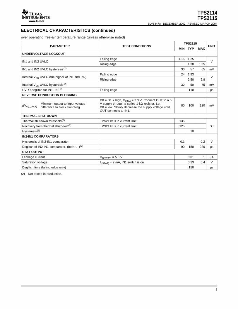
ELECTRICAL CHARACTERISTICS (continued)
over operating free-air temperature range (unless otherwise noted)
TPS2115PARAMETER TEST CONDITIONS UNIT
MIN TYP MAX
UNDERVOLTAGE LOCKOUT
Falling edge 1.15 1.25IN1 and IN2 UVLO V
Rising edge 1.30 1.35
IN1 and IN2 UVLO hysteresis (2) 30 57 65 mV
Falling edge 24 2.53Internal VDD UVLO (the higher of IN1 and IN2) V
Rising edge 2.58 2.8
Internal VDD UVLO hysteresis (2) 30 50 75 mV
UVLO deglitch for IN1, IN2 (2) Falling edge 110 µs
REVERSE CONDUCTION BLOCKING
D0 = D1 = high, VI(INx) = 3.3 V. Connect OUT to a 5Minimum output-to-input voltage V supply through a series 1-kΩ resistor. Let∆VO(I_block) 80 100 120 mVdifference to block switching D0 = low. Slowly decrease the supply voltage until
OUT connects to IN1.
THERMAL SHUTDOWN
Thermal shutdown threshold (2) TPS211x is in current limit. 135
Recovery from thermal shutdown (2) TPS211x is in current limit. 125 °C
Hysteresis (2) 10
IN2-IN1 COMPARATORS
Hysteresis of IN2-IN1 comparator 0.1 0.2 V
Deglitch of IN2-IN1 comparator, (both↑↓ ) (2) 90 150 220 µs
STAT OUTPUT
Leakage current VO(STAT) = 5.5 V 0.01 1 µA
Saturation voltage II(STAT) = 2 mA, IN1 switch is on 0.13 0.4 V
Deglitch time (falling edge only) 150 µs
(2) Not tested in production.
5
www.ti.com
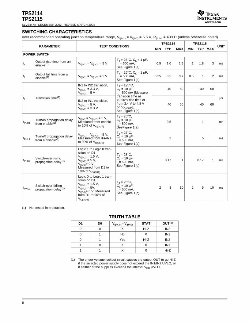
SWITCHING CHARACTERISTICS
TRUTH TABLE
TPS2114TPS2115SLVS447A–DECEMBER 2002–REVISED MARCH 2004
over recommended operating junction temperature range, VI(IN1) = VI(IN2) = 5.5 V, R(ILIM) = 400 Ω (unless otherwise noted)
TPS2114 TPS2115PARAMETER TEST CONDITIONS UNIT
MIN TYP MAX MIN TYP MAX
POWER SWITCH
TJ = 25°C, CL = 1 µF,Output rise time from antr VI(IN1) = VI(IN2) = 5 V IL = 500 mA, 0.5 1.0 1.5 1 1.8 3 msenable (1)See Figure 1(a)
TJ = 25°C, CL = 1 µF,Output fall time from atf VI(IN1) = VI(IN2) = 5 V IL = 500 mA, 0.35 0.5 0.7 0.5 1 2 msdisable (1)See Figure 1(a)
IN1 to IN2 transition, TJ = 125°C,VI(IN1) = 3.3 V, CL = 10 µF, 40 60 40 60VI(IN2) = 5 V IL= 500 mA [Measure
transition time astt Transition time (1) µs10-90% rise time orIN2 to IN1 transition,from 3.4 V to 4.8 VVI(IN1) = 5 V, 40 60 40 60on VO(OUT)],VI(IN2) = 3.3 VSee Figure 1(b)
TJ = 25°C,VI(IN1)= VI(IN2) = 5 V,Turnon propagation delay CL = 10 µF,tPLH1 Measured from enable 0.5 1 msfrom enable (1) IL= 500 mA,to 10% of VO(OUT) SeeFigure 1(a)
TJ = 25°C,VI(IN1) = VI(IN2) = 5 V,Turnoff propagation delay CL = 10 µF,tPHL1 Measured from disable 3 5 msfrom a disable (1) IL= 500 mA,to 90% of VO(OUT) See Figure 1(a)
Logic 1 to Logic 0 tran-sition on D1, TJ = 25°C,VI(IN1) = 1.5 V,Switch-over rising CL = 10 µF,tPLH2 VI(IN2) = 5 V, 0.17 1 0.17 1 mspropagation delay (1) IL= 500 mA,VI(D0)= 0 V, See Figure 1(c)Measured from D1 to10% of VO(OUT)
Logic 0 to Logic 1 tran-sition on D1, TJ = 25°C,VI(IN1) = 1.5 V,Switch-over falling CL = 10 µF,tPHL2 VI(IN2) = 5V, 2 3 10 2 5 10 mspropagation delay (1) IL= 500 mA,VI(D0)= 0 V, Measured See Figure 1(c)from D1 to 90% ofVO(OUT)
(1) Not tested in production.
D1 D0 VI(IN2) > VI(IN1) STAT OUT (1)
0 0 X Hi-Z IN2
0 1 No 0 IN1
0 1 Yes Hi-Z IN2
1 0 X 0 IN1
1 1 X 0 Hi-Z
(1) The under-voltage lockout circuit causes the output OUT to go Hi-Zif the selected power supply does not exceed the IN1/IN2 UVLO, orif neither of the supplies exceeds the internal VDD UVLO.
6

www.ti.com
FUNCTIONAL BLOCK DIAGRAM
Q2 is ON
1STAT
ControlLogic
D1
D0
UVLO (IN1)
UVLO (IN2)
UVLO (VDD)
Q2 is ON Q1 is ON
_+
_+
+0.6 V
EN2 EN1
Cross-ConductionDetector
_
+
Q2
Q1
ChargePump
0.5 V
TPS2114: k = 0.2%TPS2115: k = 0.1%
k* IO(OUT)
_+VO(OUT) > VI(INx)
+100 mV
_+
IO(OUT)
Vf = 0 V
EN1
IN2
IN1
7
4
OUT
ILIM
Internal VDD
Vf = 0 V
VDDULVO
ThermalSense
1 µA
IN2ULVO
1 µA
IN1ULVO
8
6
2
3
5
IN1
IN2
D0
D1
GND
TPS2114TPS2115
SLVS447A–DECEMBER 2002–REVISED MARCH 2004
Terminal Functions
TERMINALI/O DESCRIPTION
NAME NO.
D0 2 I TTL and CMOS compatible input pins. Each pin has a 1-µA pullup resistor. The truth table shown above illustratesthe functionality of D0 and D1.D1 3 I
GND 5 I Ground
IN1 8 I Primary power switch input. The IN1 switch can be enabled only if the IN1 supply is above the UVLO threshold andat least one supply exceeds the internal VDD UVLO.
IN2 6 I Secondary power switch input. The IN2 switch can be enabled only if the IN2 supply is above the UVLO thresholdand at least one supply exceeds the internal VDD UVLO.
ILIM 4 I A resistor R(ILIM) from ILIM to GND sets the current limit IL to 250/R(ILIM) and 500/R(ILIM) for the TPS2114 andTPS2115, respectively.
OUT 7 O Power switch output
STAT 1 O STAT is an open-drain output that is Hi-Z if the IN2 switch is ON. STAT pulls low if the IN1 switch is ON or if OUT isHi-Z (i.e., EN is equal to logic 0).
7

www.ti.com
PARAMETER MEASUREMENT INFORMATION
0 V 10%
90%
Switch EnabledSwitch Off Switch Off
90%
10%
3.3 V
5 V
Switch #1 Enabled Switch #2 Enabled
4.8 V
3.4 V
DO-D1
1.5 V1.85 V
4.65 V
Switch #2 EnabledSwitch #1 Enabled Switch #1 Enabled
5 V
tr tf
tPLH1 tPHL1
VO(OUT)
tt
VO(OUT)
VO(OUT)
DO-D1tPLH2 tPHL2
(a)
(b)
(c)
DO-D1
TPS2114TPS2115SLVS447A–DECEMBER 2002–REVISED MARCH 2004
Figure 1. Propagation Delays and Transition Timing Waveforms
8

www.ti.com
TYPICAL CHARACTERISTICS
VI(DO)
VI(D1)
VO(OUT)
t - Time - 1 ms/div
2V/Div
2V/Div
2V/Div
STAT
D0
D1
ILIM
IN1
OUT
IN2
GND
1
2
3
4
8
7
6
5
TPS2115PW 0.1 µF
0.1 µF
50 Ω
5 V
3.3 V
400 Ω
f = 28 Hz78% Duty Cycle
Output Switchover Response Test Circuit
OUTPUT SWITCHOVER RESPONSE
NC
1µF
t − Time − 2 ms/div
VI(DO)
VI(D1)
VO(OUT)
2V/Div
2V/Div
2V/Div
STAT
D0
D1
ILIM
IN1
OUT
IN2
GND
1
2
3
4
8
7
6
5
TPS2115PW 0.1 µF
0.1 µF
50 Ω
5 V
3.3 V
400 Ω
f = 28 Hz78% Duty Cycle
1µF
OUTPUT TURNON RESPONSE
Output Turnon Response Test Circuit
NC
TPS2114TPS2115
SLVS447A–DECEMBER 2002–REVISED MARCH 2004
Figure 2.
Figure 3.
9

www.ti.com
CL = 1 µF
CL = 0 µF
t - Time - 40 µs/div
VI(DO)
VI(D1)
VO(OUT)
2V/Div
2V/Div
2V/Div
Output Switchover Voltage Droop Test Circuit
OUTPUT SWITCHOVER VOLTAGE DROOP
STAT
D0
D1
ILIM
IN1
OUT
IN2
GND
1
2
3
4
8
7
6
5
TPS2115PW 0.1 µF
0.1 µF
50 Ω
400 Ω
f = 580 Hz90% Duty Cycle
5 V
NC
0 µF
CL
TPS2114TPS2115SLVS447A–DECEMBER 2002–REVISED MARCH 2004
TYPICAL CHARACTERISTICS (continued)
Figure 4.
10
www.ti.com
0
0.5
1
1.5
2
2.5
3
3.5
4
4.5
5
0.1 1 10 100
RL = 10 Ω
RL = 50 Ω
VI = 5 V
- O
utp
ut
Vo
ltag
e D
roo
p -
V
CL - Load Capacitance - µF
OUTPUT SWITCHOVER VOLTAGE DROOPvs
LOAD CAPACITANCE
D0
D1
VSNS
ILIM
IN1
OUT
IN2
GND
1
2
3
4
8
7
6
5
TPS2115PW0.1 µF
0.1 µF
VI
400 Ω
0.1 µF 1 µF 10 µF 47 µF 100 µF50 Ω 10 Ω
f = 28 Hz50% Duty Cycle
Output Switchover Voltage Droop Test Circuit
O(O
UT
)∆
V
NC
TPS2114TPS2115
SLVS447A–DECEMBER 2002–REVISED MARCH 2004
TYPICAL CHARACTERISTICS (continued)
Figure 5.
11

www.ti.com
0
50
100
150
200
250
300
0 20 40 60 80 100
VI = 5 V
VI = 3.3 V
Inru
sh C
urr
ent
- m
A
CL - Load Capacitance - µF
INRUSH CURRENTvs
LOAD CAPACITANCE
STAT
D0
D1
ILIM
IN1
OUT
IN2
GND
1
2
3
4
8
7
6
5
TPS2115PW0.1 µF
0.1 µF
VI
400 Ω
0.1 µF 47 µF10 µF
50 Ω
To Oscilloscope
1 µF 100 µF
f = 28 Hz90% Duty Cycle
Output Capacitor Inrush Current Test Circuit
II
-
NC
NC
TPS2114TPS2115SLVS447A–DECEMBER 2002–REVISED MARCH 2004
TYPICAL CHARACTERISTICS (continued)
Figure 6.
12

www.ti.com
−50 0 50 100 150TJ − Junction Temperature − °C
60
80
100
120
140
160
180
TPS2114
TPS2115
− S
witc
h O
n-R
esis
tan
ce −
mΩ
r DS
(on
)
2 3 4 5 6VI(INx) − Supply Voltage − V
80
85
90
95
100
105
110
115
120
TPS2114
TPS2115
− S
witc
h O
n-R
esis
tan
ce −
mΩ
r DS
(on
)
40
42
44
46
48
50
52
54
56
58
60
2 3 4 5 6VI(IN1) − Supply Voltage − V
I(IN
1)−
IN1
Su
pp
ly C
urr
ent −
Aµ
IN1 Switch is ONVI(IN2) = 0 V,IO(OUT) = 0 A
I
0.82
0.84
0.86
0.88
0.90
0.92
0.94
0.96
2 3 4 5 6
I(IN
1)A
µ
VI(IN1)− IN1 Supply Voltage − V
Device DisabledVI(IN2) = 0 VIO(OUT) = 0 A
I−
IN1
Su
pp
ly C
urr
ent −
TPS2114TPS2115
SLVS447A–DECEMBER 2002–REVISED MARCH 2004
TYPICAL CHARACTERISTICS (continued)
SWITCH ON-RESISTANCE SWITCH ON-RESISTANCEvs vs
JUNCTION TEMPERATURE SUPPLY VOLTAGE
Figure 7. Figure 8.
IN1 SUPPLY CURRENT IN1 SUPPLY CURRENTvs vs
SUPPLY VOLTAGE SUPPLY VOLTAGE
Figure 9. Figure 10.
13

www.ti.com
0
10
20
30
40
50
60
70
80
−50 0 50 100 150
II(IN1)
II(IN2)
TJ − Junction Temperature − °C
IN1 Switch is ONVI(IN1) = 5.5 V,VI(IN2) = 3.3 VIO(OUT) = 0 A
I(IN
x)S
up
ply
Cu
rren
t −
−A
µI
0
0.2
0.4
0.6
0.8
1
1.2
−50 0 50 100 150
II(IN1) = 5.5 V
II(IN2) = 3.3 V
Device Disabled
TJ − Junction Temperature − °C
I(IN
x)S
up
ply
Cu
rren
t −
−A
µ
VI(IN1) = 5.5 V
VI(IN2) = 3.3 VIO(OUT) = 0 A
I
TPS2114TPS2115SLVS447A–DECEMBER 2002–REVISED MARCH 2004
TYPICAL CHARACTERISTICS (continued)
SUPPLY CURRENT SUPPLY CURRENTvs vs
JUNCTION TEMPERATURE JUNCTION TEMPERATURE
Figure 11. Figure 12.
14

www.ti.com
APPLICATION INFORMATION
STAT
D0
D1
ILIM
IN1
OUT
IN2
GND
1
2
3
4
8
7
6
5
TPS2115PW 0.1 µF
C20.1 µF
CL RL
IN1: 2.8 - 5.5 V
IN2: 2.8 - 5.5 V
RILIM
NC
Switch Status
R1
STAT
D0
D1
ILIM
IN1
OUT
IN2
GND
1
2
3
4
8
7
6
5
TPS2115PW 0.1 µF
0.1 µF
CL RL
IN1: 2.8 - 5.5 V
IN2: 2.8 - 5.5 V
RILIM
Switch Status
R1
TPS2114TPS2115
SLVS447A–DECEMBER 2002–REVISED MARCH 2004
The circuit in Figure 13 allows one or two battery packs to power a system. Two battery packs allow a longer runtime. The TPS2114/5 cycles between the battery packs until both packs are drained.
Figure 13. Running a System From Two Battery Packs
In Figure 14, the multiplexer selects between two power supplies based upon the D1 logic signal. OUT connectsto IN1 if D1 is logic 1, otherwise OUT connects to IN2. The logic thresholds for the D1 terminal are compatiblewith both TTL and CMOS logic.
Figure 14. Manually Switching Power Sources
15

www.ti.com
DETAILED DESCRIPTION
AUTO-SWITCHING MODE
MANUAL SWITCHING MODE
N-CHANNEL MOSFETs
CROSS-CONDUCTION BLOCKING
REVERSE-CONDUCTION BLOCKING
CHARGE PUMP
CURRENT LIMITING
OUTPUT VOLTAGE SLEW-RATE CONTROL
TPS2114TPS2115SLVS447A–DECEMBER 2002–REVISED MARCH 2004
D0 equal to logic 1 and D1 equal to logic 0 selects the auto-switching mode. In this mode, OUT connects to thehigher of IN1 and IN2.
D0 equal to logic 0 selects the manual-switching mode. In this mode, OUT connects to IN1 if D1 is equal to logic1, otherwise OUT connects to IN2.
Two internal high-side power MOSFETs implement a single-pole double-throw (SPDT) switch. Digital logicselects the IN1 switch, IN2 switch, or no switch (Hi-Z state). The MOSFETs have no parallel diodes sooutput-to-input current cannot flow when the FET is off. An integrated comparator prevents turnon of a FETswitch if the output voltage is greater than the input voltage.
The switching circuitry ensures that both power switches never conduct at the same time. A comparator monitorsthe gate-to-source voltage of each power FET and allows a FET to turn on only if the gate-to-source voltage ofthe other FET is below the turnon threshold voltage.
When the TPS211x switches from a higher-voltage supply to a lower-voltage supply, current can potentially flowback from the load capacitor into the lower-voltage supply. To minimize such reverse conduction, the TPS211xdoes not connect a supply to the output until the output voltage has fallen to within 100 mV of the supply voltage.Once a supply has been connected to the output, it remains connected regardless of output voltage.
The higher of supplies IN1 and IN2 powers the internal charge pump. The charge pump provides power to thecurrent limit amplifier and allows the output FET gate voltage to be higher than the IN1 and IN2 supply voltages.A gate voltage that is higher than the source voltage is necessary to turn on the N-channel FET.
A resistor R(ILIM) from ILIM to GND sets the current limit to 250/ R(ILIM) and 500/R(ILIM) for the TPS2114 andTPS2115, respectively. Setting resistor R(ILIM) equal to zero is not recommended as that disables current limiting.
The TPS2114/5 slews the output voltage at a slow rate when OUT switches to IN1 or IN2 from the Hi-Z state(see Truth Table). A slow slew rate limits the inrush current into the load capacitor. High inrush currents canadversely effect the voltage bus and cause a system to hang up or reset. It can also cause reliability issues—likepit the connector power contacts, when hot plugging a load like a PCI card. The TPS2114/5 slews the outputvoltage at a much faster rate when OUT switches between IN1 and IN2. The fast rate minimizes the outputvoltage droop and reduces the output voltage hold-up capacitance requirement.
16

PACKAGE OPTION ADDENDUM
www.ti.com 8-Nov-2014
Addendum-Page 1
PACKAGING INFORMATION
Orderable Device Status(1)
Package Type PackageDrawing
Pins PackageQty
Eco Plan(2)
Lead/Ball Finish(6)
MSL Peak Temp(3)
Op Temp (°C) Device Marking(4/5)
Samples
TPS2114PW ACTIVE TSSOP PW 8 150 Green (RoHS& no Sb/Br)
CU NIPDAU Level-1-260C-UNLIM -40 to 85 2114
TPS2114PWG4 ACTIVE TSSOP PW 8 150 Green (RoHS& no Sb/Br)
CU NIPDAU Level-1-260C-UNLIM -40 to 85 2114
TPS2115PW ACTIVE TSSOP PW 8 150 Green (RoHS& no Sb/Br)
CU NIPDAU Level-1-260C-UNLIM -40 to 85 2115
TPS2115PWG4 ACTIVE TSSOP PW 8 150 Green (RoHS& no Sb/Br)
CU NIPDAU Level-1-260C-UNLIM -40 to 85 2115
TPS2115PWR ACTIVE TSSOP PW 8 2000 Green (RoHS& no Sb/Br)
CU NIPDAU Level-1-260C-UNLIM -40 to 85 2115
TPS2115PWRG4 ACTIVE TSSOP PW 8 2000 Green (RoHS& no Sb/Br)
CU NIPDAU Level-1-260C-UNLIM -40 to 85 2115
(1) The marketing status values are defined as follows:ACTIVE: Product device recommended for new designs.LIFEBUY: TI has announced that the device will be discontinued, and a lifetime-buy period is in effect.NRND: Not recommended for new designs. Device is in production to support existing customers, but TI does not recommend using this part in a new design.PREVIEW: Device has been announced but is not in production. Samples may or may not be available.OBSOLETE: TI has discontinued the production of the device.
(2) Eco Plan - The planned eco-friendly classification: Pb-Free (RoHS), Pb-Free (RoHS Exempt), or Green (RoHS & no Sb/Br) - please check http://www.ti.com/productcontent for the latest availabilityinformation and additional product content details.TBD: The Pb-Free/Green conversion plan has not been defined.Pb-Free (RoHS): TI's terms "Lead-Free" or "Pb-Free" mean semiconductor products that are compatible with the current RoHS requirements for all 6 substances, including the requirement thatlead not exceed 0.1% by weight in homogeneous materials. Where designed to be soldered at high temperatures, TI Pb-Free products are suitable for use in specified lead-free processes.Pb-Free (RoHS Exempt): This component has a RoHS exemption for either 1) lead-based flip-chip solder bumps used between the die and package, or 2) lead-based die adhesive used betweenthe die and leadframe. The component is otherwise considered Pb-Free (RoHS compatible) as defined above.Green (RoHS & no Sb/Br): TI defines "Green" to mean Pb-Free (RoHS compatible), and free of Bromine (Br) and Antimony (Sb) based flame retardants (Br or Sb do not exceed 0.1% by weightin homogeneous material)
(3) MSL, Peak Temp. - The Moisture Sensitivity Level rating according to the JEDEC industry standard classifications, and peak solder temperature.
(4) There may be additional marking, which relates to the logo, the lot trace code information, or the environmental category on the device.
(5) Multiple Device Markings will be inside parentheses. Only one Device Marking contained in parentheses and separated by a "~" will appear on a device. If a line is indented then it is a continuationof the previous line and the two combined represent the entire Device Marking for that device.

PACKAGE OPTION ADDENDUM
www.ti.com 8-Nov-2014
Addendum-Page 2
(6) Lead/Ball Finish - Orderable Devices may have multiple material finish options. Finish options are separated by a vertical ruled line. Lead/Ball Finish values may wrap to two lines if the finishvalue exceeds the maximum column width.
Important Information and Disclaimer:The information provided on this page represents TI's knowledge and belief as of the date that it is provided. TI bases its knowledge and belief on informationprovided by third parties, and makes no representation or warranty as to the accuracy of such information. Efforts are underway to better integrate information from third parties. TI has taken andcontinues to take reasonable steps to provide representative and accurate information but may not have conducted destructive testing or chemical analysis on incoming materials and chemicals.TI and TI suppliers consider certain information to be proprietary, and thus CAS numbers and other limited information may not be available for release.
In no event shall TI's liability arising out of such information exceed the total purchase price of the TI part(s) at issue in this document sold by TI to Customer on an annual basis.

TAPE AND REEL INFORMATION
*All dimensions are nominal
Device PackageType
PackageDrawing
Pins SPQ ReelDiameter
(mm)
ReelWidth
W1 (mm)
A0(mm)
B0(mm)
K0(mm)
P1(mm)
W(mm)
Pin1Quadrant
TPS2115PWR TSSOP PW 8 2000 330.0 12.4 7.0 3.6 1.6 8.0 12.0 Q1
PACKAGE MATERIALS INFORMATION
www.ti.com 11-Jun-2013
Pack Materials-Page 1

*All dimensions are nominal
Device Package Type Package Drawing Pins SPQ Length (mm) Width (mm) Height (mm)
TPS2115PWR TSSOP PW 8 2000 367.0 367.0 35.0
PACKAGE MATERIALS INFORMATION
www.ti.com 11-Jun-2013
Pack Materials-Page 2

www.ti.com
PACKAGE OUTLINE
C
TYP6.66.2
1.2 MAX
6X 0.65
8X 0.300.19
2X1.95
0.150.05
(0.15) TYP
0 - 8
0.25GAGE PLANE
0.750.50
A
NOTE 3
3.12.9
BNOTE 4
4.54.3
4221848/A 02/2015
TSSOP - 1.2 mm max heightPW0008ASMALL OUTLINE PACKAGE
NOTES: 1. All linear dimensions are in millimeters. Any dimensions in parenthesis are for reference only. Dimensioning and tolerancing per ASME Y14.5M. 2. This drawing is subject to change without notice. 3. This dimension does not include mold flash, protrusions, or gate burrs. Mold flash, protrusions, or gate burrs shall not exceed 0.15 mm per side. 4. This dimension does not include interlead flash. Interlead flash shall not exceed 0.25 mm per side.5. Reference JEDEC registration MO-153, variation AA.
18
0.1 C A B
54
PIN 1 IDAREA
SEATING PLANE
0.1 C
SEE DETAIL A
DETAIL ATYPICAL
SCALE 2.800
www.ti.com
EXAMPLE BOARD LAYOUT
(5.8)
0.05 MAXALL AROUND
0.05 MINALL AROUND
8X (1.5)8X (0.45)
6X (0.65)
(R )TYP
0.05
4221848/A 02/2015
TSSOP - 1.2 mm max heightPW0008ASMALL OUTLINE PACKAGE
SYMM
SYMM
LAND PATTERN EXAMPLESCALE:10X
1
45
8
NOTES: (continued) 6. Publication IPC-7351 may have alternate designs. 7. Solder mask tolerances between and around signal pads can vary based on board fabrication site.
METALSOLDER MASKOPENING
NON SOLDER MASKDEFINED
SOLDER MASK DETAILSNOT TO SCALE
SOLDER MASKOPENING
METAL UNDERSOLDER MASK
SOLDER MASKDEFINED

www.ti.com
EXAMPLE STENCIL DESIGN
(5.8)
6X (0.65)
8X (0.45)8X (1.5)
(R ) TYP0.05
4221848/A 02/2015
TSSOP - 1.2 mm max heightPW0008ASMALL OUTLINE PACKAGE
NOTES: (continued) 8. Laser cutting apertures with trapezoidal walls and rounded corners may offer better paste release. IPC-7525 may have alternate design recommendations. 9. Board assembly site may have different recommendations for stencil design.
SYMM
SYMM
1
45
8
SOLDER PASTE EXAMPLEBASED ON 0.125 mm THICK STENCIL
SCALE:10X

IMPORTANT NOTICE
Texas Instruments Incorporated and its subsidiaries (TI) reserve the right to make corrections, enhancements, improvements and otherchanges to its semiconductor products and services per JESD46, latest issue, and to discontinue any product or service per JESD48, latestissue. Buyers should obtain the latest relevant information before placing orders and should verify that such information is current andcomplete. All semiconductor products (also referred to herein as “components”) are sold subject to TI’s terms and conditions of salesupplied at the time of order acknowledgment.TI warrants performance of its components to the specifications applicable at the time of sale, in accordance with the warranty in TI’s termsand conditions of sale of semiconductor products. Testing and other quality control techniques are used to the extent TI deems necessaryto support this warranty. Except where mandated by applicable law, testing of all parameters of each component is not necessarilyperformed.TI assumes no liability for applications assistance or the design of Buyers’ products. Buyers are responsible for their products andapplications using TI components. To minimize the risks associated with Buyers’ products and applications, Buyers should provideadequate design and operating safeguards.TI does not warrant or represent that any license, either express or implied, is granted under any patent right, copyright, mask work right, orother intellectual property right relating to any combination, machine, or process in which TI components or services are used. Informationpublished by TI regarding third-party products or services does not constitute a license to use such products or services or a warranty orendorsement thereof. Use of such information may require a license from a third party under the patents or other intellectual property of thethird party, or a license from TI under the patents or other intellectual property of TI.Reproduction of significant portions of TI information in TI data books or data sheets is permissible only if reproduction is without alterationand is accompanied by all associated warranties, conditions, limitations, and notices. TI is not responsible or liable for such altereddocumentation. Information of third parties may be subject to additional restrictions.Resale of TI components or services with statements different from or beyond the parameters stated by TI for that component or servicevoids all express and any implied warranties for the associated TI component or service and is an unfair and deceptive business practice.TI is not responsible or liable for any such statements.Buyer acknowledges and agrees that it is solely responsible for compliance with all legal, regulatory and safety-related requirementsconcerning its products, and any use of TI components in its applications, notwithstanding any applications-related information or supportthat may be provided by TI. Buyer represents and agrees that it has all the necessary expertise to create and implement safeguards whichanticipate dangerous consequences of failures, monitor failures and their consequences, lessen the likelihood of failures that might causeharm and take appropriate remedial actions. Buyer will fully indemnify TI and its representatives against any damages arising out of the useof any TI components in safety-critical applications.In some cases, TI components may be promoted specifically to facilitate safety-related applications. With such components, TI’s goal is tohelp enable customers to design and create their own end-product solutions that meet applicable functional safety standards andrequirements. Nonetheless, such components are subject to these terms.No TI components are authorized for use in FDA Class III (or similar life-critical medical equipment) unless authorized officers of the partieshave executed a special agreement specifically governing such use.Only those TI components which TI has specifically designated as military grade or “enhanced plastic” are designed and intended for use inmilitary/aerospace applications or environments. Buyer acknowledges and agrees that any military or aerospace use of TI componentswhich have not been so designated is solely at the Buyer's risk, and that Buyer is solely responsible for compliance with all legal andregulatory requirements in connection with such use.TI has specifically designated certain components as meeting ISO/TS16949 requirements, mainly for automotive use. In any case of use ofnon-designated products, TI will not be responsible for any failure to meet ISO/TS16949.
Products ApplicationsAudio www.ti.com/audio Automotive and Transportation www.ti.com/automotiveAmplifiers amplifier.ti.com Communications and Telecom www.ti.com/communicationsData Converters dataconverter.ti.com Computers and Peripherals www.ti.com/computersDLP® Products www.dlp.com Consumer Electronics www.ti.com/consumer-appsDSP dsp.ti.com Energy and Lighting www.ti.com/energyClocks and Timers www.ti.com/clocks Industrial www.ti.com/industrialInterface interface.ti.com Medical www.ti.com/medicalLogic logic.ti.com Security www.ti.com/securityPower Mgmt power.ti.com Space, Avionics and Defense www.ti.com/space-avionics-defenseMicrocontrollers microcontroller.ti.com Video and Imaging www.ti.com/videoRFID www.ti-rfid.comOMAP Applications Processors www.ti.com/omap TI E2E Community e2e.ti.comWireless Connectivity www.ti.com/wirelessconnectivity
Mailing Address: Texas Instruments, Post Office Box 655303, Dallas, Texas 75265Copyright © 2015, Texas Instruments Incorporated