Autonomous USB PD controller with short-to-VBUS …content/translations/en.DM00356577.pdfDecember...
35
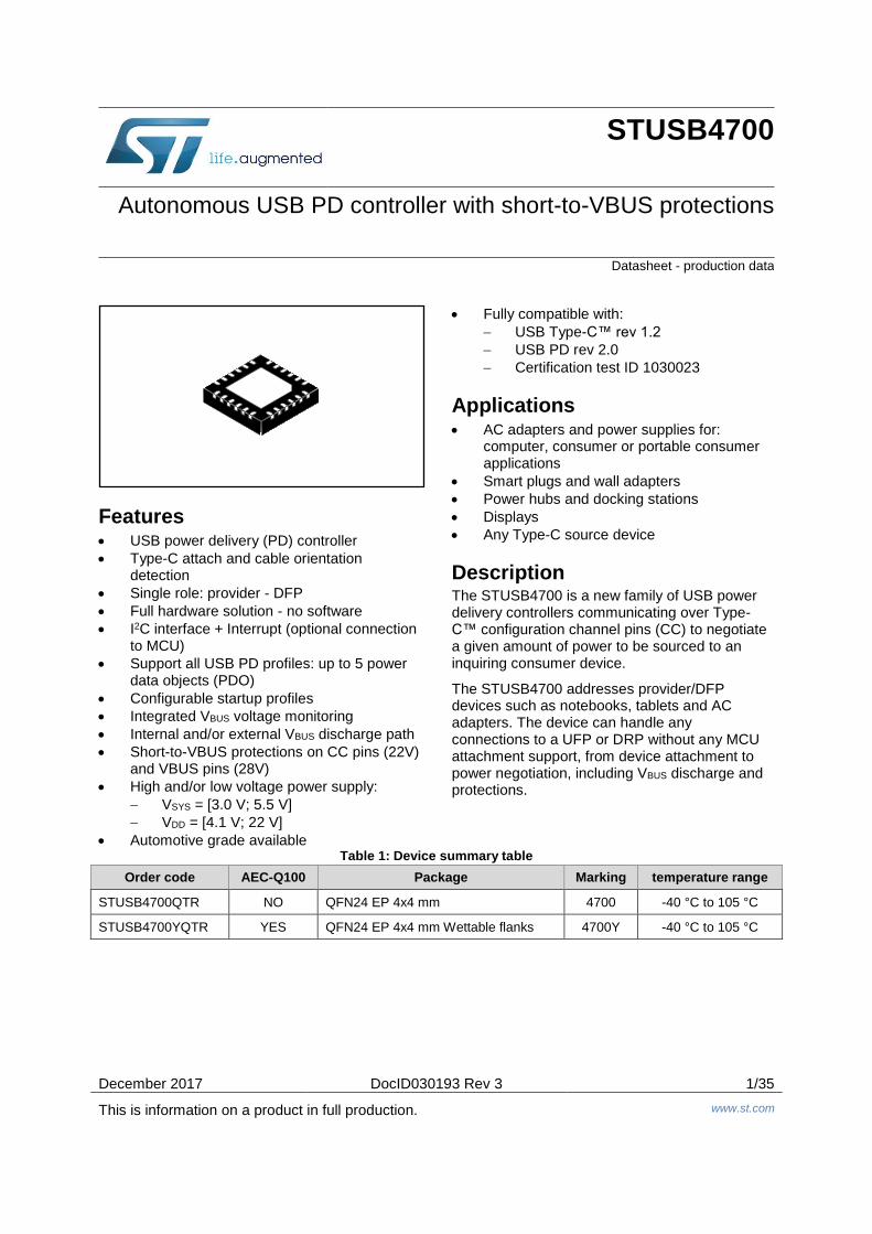
December 2017 DocID030193 Rev 3 1/35 This is information on a product in full production. www.st.com STUSB4700 Autonomous USB PD controller with short-to-VBUS protections Datasheet - production data Features USB power delivery (PD) controller Type-C attach and cable orientation detection Single role: provider - DFP Full hardware solution - no software I 2 C interface + Interrupt (optional connection to MCU) Support all USB PD profiles: up to 5 power data objects (PDO) Configurable startup profiles Integrated VBUS voltage monitoring Internal and/or external VBUS discharge path Short-to-VBUS protections on CC pins (22V) and VBUS pins (28V) High and/or low voltage power supply: VSYS = [3.0 V; 5.5 V] VDD = [4.1 V; 22 V] Automotive grade available Fully compatible with: USB Type-C™ rev 1.2 USB PD rev 2.0 Certification test ID 1030023 Applications AC adapters and power supplies for: computer, consumer or portable consumer applications Smart plugs and wall adapters Power hubs and docking stations Displays Any Type-C source device Description The STUSB4700 is a new family of USB power delivery controllers communicating over Type- C™ configuration channel pins (CC) to negotiate a given amount of power to be sourced to an inquiring consumer device. The STUSB4700 addresses provider/DFP devices such as notebooks, tablets and AC adapters. The device can handle any connections to a UFP or DRP without any MCU attachment support, from device attachment to power negotiation, including VBUS discharge and protections. Table 1: Device summary table Order code AEC-Q100 Package Marking temperature range STUSB4700QTR NO QFN24 EP 4x4 mm 4700 -40 °C to 105 °C STUSB4700YQTR YES QFN24 EP 4x4 mm Wettable flanks 4700Y -40 °C to 105 °C
-
Upload
trinhhuong -
Category
Documents
-
view
228 -
download
1
Transcript of Autonomous USB PD controller with short-to-VBUS …content/translations/en.DM00356577.pdfDecember...
December 2017 DocID030193 Rev 3 1/35
This is information on a product in full production. www.st.com
STUSB4700
Autonomous USB PD controller with short-to-VBUS protections
Datasheet - production data
Features USB power delivery (PD) controller
Type-C attach and cable orientation detection
Single role: provider - DFP
Full hardware solution - no software
I2C interface + Interrupt (optional connection to MCU)
Support all USB PD profiles: up to 5 power data objects (PDO)
Configurable startup profiles
Integrated VBUS voltage monitoring
Internal and/or external VBUS discharge path
Short-to-VBUS protections on CC pins (22V) and VBUS pins (28V)
High and/or low voltage power supply:
VSYS = [3.0 V; 5.5 V]
VDD = [4.1 V; 22 V]
Automotive grade available
Fully compatible with:
USB Type-C™ rev 1.2
USB PD rev 2.0
Certification test ID 1030023
Applications AC adapters and power supplies for:
computer, consumer or portable consumer applications
Smart plugs and wall adapters
Power hubs and docking stations
Displays
Any Type-C source device
Description The STUSB4700 is a new family of USB power delivery controllers communicating over Type-C™ configuration channel pins (CC) to negotiate a given amount of power to be sourced to an inquiring consumer device.
The STUSB4700 addresses provider/DFP devices such as notebooks, tablets and AC adapters. The device can handle any connections to a UFP or DRP without any MCU attachment support, from device attachment to power negotiation, including VBUS discharge and protections.
Table 1: Device summary table
Order code AEC-Q100 Package Marking temperature range
STUSB4700QTR NO QFN24 EP 4x4 mm 4700 -40 °C to 105 °C
STUSB4700YQTR YES QFN24 EP 4x4 mm Wettable flanks 4700Y -40 °C to 105 °C
Contents STUSB4700
2/35 DocID030193 Rev 3
Contents
1 Functional description .................................................................... 6
2 Inputs/outputs ................................................................................. 7
2.1 Pinout ................................................................................................ 7
2.2 Pin list ............................................................................................... 7
2.3 Pin description ................................................................................... 8
2.3.1 CC1 / CC2 .......................................................................................... 8
2.3.2 RESET ................................................................................................ 9
2.3.3 I2C interface pins ................................................................................ 9
2.3.4 A_B_SIDE .......................................................................................... 9
2.3.5 VBUS_SENSE .................................................................................... 9
2.3.6 VBUS_EN_SRC ................................................................................. 9
2.3.7 VSYS .................................................................................................. 9
2.3.8 VDD .................................................................................................... 9
2.3.9 GND .................................................................................................... 9
2.3.10 VVAR_ADDR0 .................................................................................. 10
2.3.11 GPIO [4:0] ......................................................................................... 10
2.3.12 VREG2V7 ......................................................................................... 10
2.3.13 VREG1V2 ......................................................................................... 10
2.3.14 VBUS_DISCH ................................................................................... 10
2.3.15 VCONN ............................................................................................. 10
3 Block descriptions ........................................................................ 11
3.1 CC interface .................................................................................... 11
3.2 BMC ................................................................................................ 11
3.3 Protocol layer .................................................................................. 11
3.4 Policy engine ................................................................................... 11
3.5 Device policy manager .................................................................... 12
3.6 VBUS power path control ................................................................ 12
3.6.1 VBUS monitoring .............................................................................. 12
3.6.2 VBUS discharge ............................................................................... 12
3.6.3 VBUS power path assertion ............................................................. 13
3.7 High voltage protection ................................................................... 13
3.8 Hardware fault management ........................................................... 13
3.9 Accessory mode detection .............................................................. 14
3.9.1 Audio accessory mode detection ..................................................... 14
3.9.2 Debug accessory mode detection .................................................... 14
STUSB4700 Contents
DocID030193 Rev 3 3/35
4 User-defined startup configuration .............................................. 15
4.1 Parameter overview ........................................................................ 15
4.2 PDO – voltage configuration in NVM ............................................... 15
4.3 PDO – current configuration in NVM ............................................... 16
4.4 Monitoring configuration in NVM ..................................................... 16
4.5 Discharge configuration in NVM ...................................................... 16
5 I²C interface .................................................................................... 17
5.1 Read and write operations .............................................................. 17
5.2 Timing specifications ....................................................................... 18
6 I²C register map ............................................................................. 20
7 Typical use cases .......................................................................... 22
7.1 Power supply – buck topology ......................................................... 22
7.2 Power supply – flyback topology ..................................................... 23
8 Electrical characteristics .............................................................. 24
8.1 Absolute maximum rating ................................................................ 24
8.2 Operating conditions ....................................................................... 24
8.3 Electrical and timing characteristics ................................................ 25
9 Package information ..................................................................... 28
9.1 QFN24 EP 4x4 mm package information ........................................ 28
9.2 QFN24 EP 4x4 mm wettable flank package information ................. 30
9.3 Thermal information ........................................................................ 32
9.4 Packing information ......................................................................... 32
10 Terms and abbreviations .............................................................. 33
11 Revision history ............................................................................ 34
List of tables STUSB4700
4/35 DocID030193 Rev 3
List of tables
Table 1: Device summary table .................................................................................................................. 1 Table 2: Pin functions list ............................................................................................................................ 7 Table 3: Legend .......................................................................................................................................... 8 Table 4: I2C interface pin list ...................................................................................................................... 9 Table 5: USB Data mux select .................................................................................................................... 9 Table 6: GPIO0 (pin #12) configuration .................................................................................................... 10 Table 7: GPIO1 (pin #11) configuration .................................................................................................... 10 Table 8: GPIO2 (pin #14) – GPIO3 (pin #15) – GPIO4 (pin #16) configuration ....................................... 10 Table 9: Conditions for VBUS power path assertion ................................................................................ 13 Table 10: PDO configurations in NVM ...................................................................................................... 15 Table 11: PDO NVM voltage configuration ............................................................................................... 15 Table 12: PDO NVM current configuration ............................................................................................... 16 Table 13: I2C timing parameters - VDD = 5 V .......................................................................................... 18 Table 14: STUSB4700 register map overview ......................................................................................... 20 Table 15: Register access legend ............................................................................................................ 21 Table 16: Resistor value ........................................................................................................................... 22 Table 17: Resistor value ........................................................................................................................... 23 Table 18: Absolute maximum rating ......................................................................................................... 24 Table 19: Operating conditions ................................................................................................................. 24 Table 20: Electrical characteristics ........................................................................................................... 25 Table 21: QFN24 EP 4x4 mm mechanical data ....................................................................................... 28 Table 22: Thermal information .................................................................................................................. 32 Table 23: Tape dimensions ...................................................................................................................... 32 Table 24: List of terms and abbreviations ................................................................................................. 33 Table 25: Document revision history ........................................................................................................ 34
STUSB4700 List of figures
DocID030193 Rev 3 5/35
List of figures
Figure 1: Functional block diagram ............................................................................................................. 6 Figure 2: STUSB4700 pin connections (top view) ...................................................................................... 7 Figure 3: Read operation .......................................................................................................................... 18 Figure 4: Write operation .......................................................................................................................... 18 Figure 5: I²C timing diagram ..................................................................................................................... 19 Figure 6: Power supply - buck topology.................................................................................................... 22 Figure 7: Flyback topology ........................................................................................................................ 23 Figure 8: QFN24 EP 4x4 mm package outline ......................................................................................... 28 Figure 9: QFN24 EP 4x4 mm recommended footprint ............................................................................. 29 Figure 10: QFN24 EP 4x4 mm wettable flank package outline ................................................................ 30 Figure 11: QFN24 EP 4x4 mm wettable flank recommended footprint .................................................... 31 Figure 12: Reel information ...................................................................................................................... 32
Functional description STUSB4700
6/35 DocID030193 Rev 3
1 Functional description
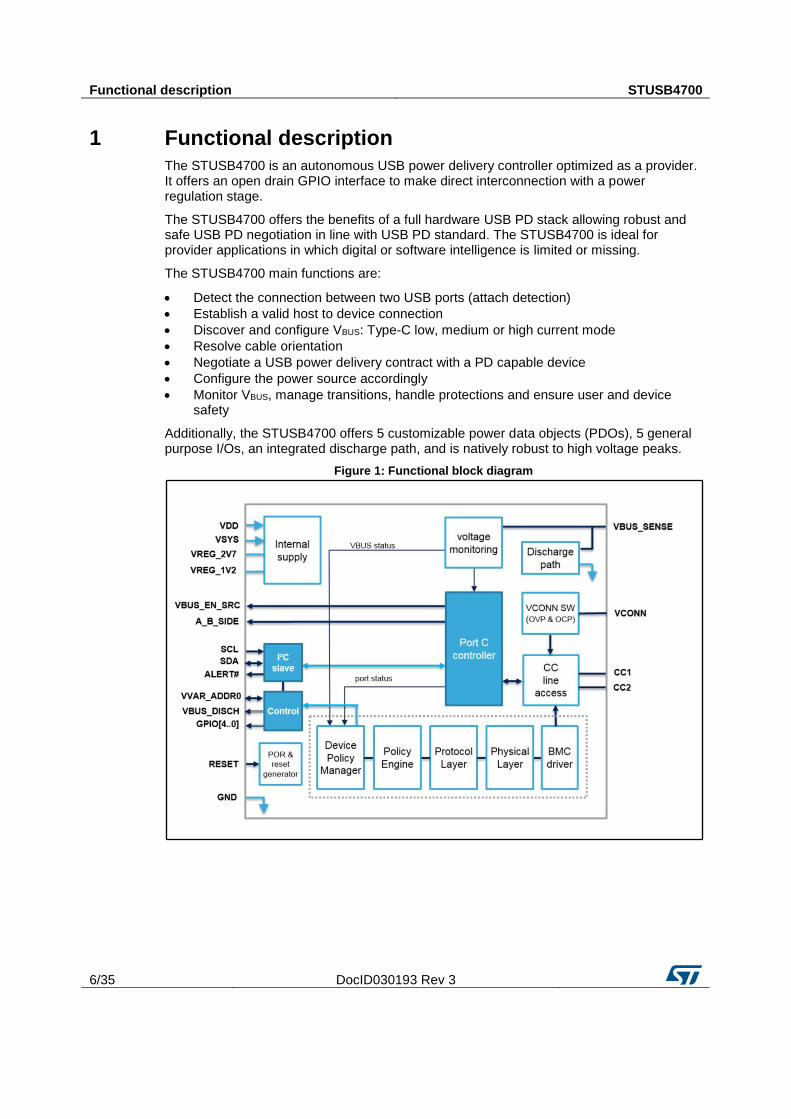
The STUSB4700 is an autonomous USB power delivery controller optimized as a provider. It offers an open drain GPIO interface to make direct interconnection with a power regulation stage.
The STUSB4700 offers the benefits of a full hardware USB PD stack allowing robust and safe USB PD negotiation in line with USB PD standard. The STUSB4700 is ideal for provider applications in which digital or software intelligence is limited or missing.
The STUSB4700 main functions are:
Detect the connection between two USB ports (attach detection)
Establish a valid host to device connection
Discover and configure VBUS: Type-C low, medium or high current mode
Resolve cable orientation
Negotiate a USB power delivery contract with a PD capable device
Configure the power source accordingly
Monitor VBUS, manage transitions, handle protections and ensure user and device safety
Additionally, the STUSB4700 offers 5 customizable power data objects (PDOs), 5 general purpose I/Os, an integrated discharge path, and is natively robust to high voltage peaks.
Figure 1: Functional block diagram
STUSB4700 Inputs/outputs
DocID030193 Rev 3 7/35
2 Inputs/outputs
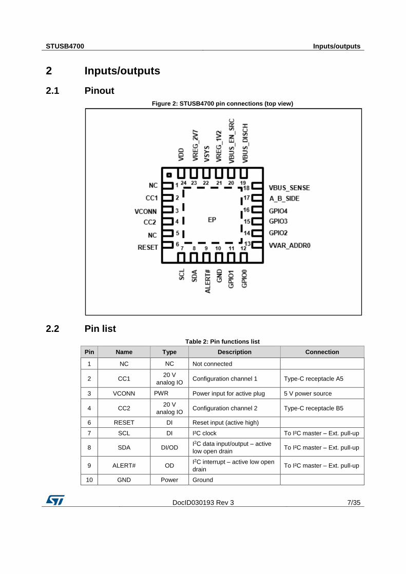
2.1 Pinout
Figure 2: STUSB4700 pin connections (top view)
2.2 Pin list
Table 2: Pin functions list
Pin Name Type Description Connection
1 NC NC Not connected
2 CC1 20 V
analog IO Configuration channel 1 Type-C receptacle A5
3 VCONN PWR Power input for active plug 5 V power source
4 CC2 20 V
analog IO Configuration channel 2 Type-C receptacle B5
6 RESET DI Reset input (active high)
7 SCL DI I²C clock To I²C master – Ext. pull-up
8 SDA DI/OD I2C data input/output – active
low open drain To I²C master – Ext. pull-up
9 ALERT# OD I2C interrupt – active low open
drain To I²C master – Ext. pull-up
10 GND Power Ground
Inputs/outputs STUSB4700
8/35 DocID030193 Rev 3
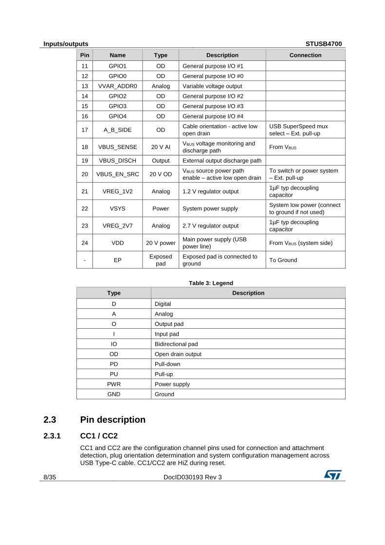
Pin Name Type Description Connection
11 GPIO1 OD General purpose I/O #1
12 GPIO0 OD General purpose I/O #0
13 VVAR_ADDR0 Analog Variable voltage output
14 GPIO2 OD General purpose I/O #2
15 GPIO3 OD General purpose I/O #3
16 GPIO4 OD General purpose I/O #4
17 A_B_SIDE OD Cable orientation - active low
open drain
USB SuperSpeed mux
select – Ext. pull-up
18 VBUS_SENSE 20 V AI VBUS voltage monitoring and
discharge path From VBUS
19 VBUS_DISCH Output External output discharge path
20 VBUS_EN_SRC 20 V OD VBUS source power path
enable – active low open drain
To switch or power system
– Ext. pull-up
21 VREG_1V2 Analog 1.2 V regulator output 1µF typ decoupling
capacitor
22 VSYS Power System power supply System low power (connect
to ground if not used)
23 VREG_2V7 Analog 2.7 V regulator output 1µF typ decoupling
capacitor
24 VDD 20 V power Main power supply (USB
power line) From VBUS (system side)
- EP Exposed
pad
Exposed pad is connected to
ground To Ground
Table 3: Legend
Type Description
D Digital
A Analog
O Output pad
I Input pad
IO Bidirectional pad
OD Open drain output
PD Pull-down
PU Pull-up
PWR Power supply
GND Ground
2.3 Pin description
2.3.1 CC1 / CC2
CC1 and CC2 are the configuration channel pins used for connection and attachment detection, plug orientation determination and system configuration management across USB Type-C cable. CC1/CC2 are HiZ during reset.
STUSB4700 Inputs/outputs
DocID030193 Rev 3 9/35
2.3.2 RESET
Active high reset. This pin resets all analog signals, states machine and reloads configuration.
2.3.3 I2C interface pins
Table 4: I2C interface pin list
Name Description
SCL I²C clock – need external pull-up
SDA I²C data – need external pull-up
ALERT# I²C interrupt – need external pull-up
2.3.4 A_B_SIDE
This output pin provides cable orientation. It is used to establish USB SuperSpeed signals routing. The cable orientation is also provided by an internal I2C register. This signal is not required in case of USB 2.0 support or in case of supply only.
Table 5: USB Data mux select
Value CC pin position
HiZ CC pin detected on CC1 (A5)
0 CC pin detected on CC2 (B5)
2.3.5 VBUS_SENSE
This input pin is used to sense VBUS presence, monitor VBUS voltage and discharge VBUS on USB Type-C receptacle side.
2.3.6 VBUS_EN_SRC
In source power role, this pin allows enabling of the outgoing VBUS power when the connection to a sink is established and VBUS is in the valid operating range. The open-drain output allows a PMOS transistor to be driven directly. The logic value of the pin is also advertised in a dedicated I2C register bit.
2.3.7 VSYS
VSYS is the low voltage power supply from the system (if any). VSYS connection is optional, and can be connected directly to a single cell Lithium battery or a system power supply delivering 3.3 V or 5 V. If not used, it is recommended to connect to GND.
2.3.8 VDD
VDD is the main power supply for applications powered by VBUS.
This pin can be used to sense the voltage level of the main power supply providing VBUS. It allows UVLO and OVLO voltage thresholds to be considered independently on VDD pin as additional conditions to enable the VBUS power path through VBUS_EN_SRC pin.
2.3.9 GND
Ground.
Inputs/outputs STUSB4700
10/35 DocID030193 Rev 3
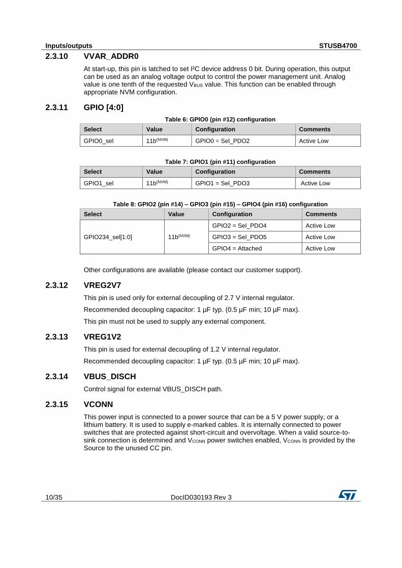
2.3.10 VVAR_ADDR0
At start-up, this pin is latched to set I²C device address 0 bit. During operation, this output can be used as an analog voltage output to control the power management unit. Analog value is one tenth of the requested VBUS value. This function can be enabled through appropriate NVM configuration.
2.3.11 GPIO [4:0]
Table 6: GPIO0 (pin #12) configuration
Select Value Configuration Comments
GPIO0_sel 11b(NVM) GPIO0 = Sel_PDO2 Active Low
Table 7: GPIO1 (pin #11) configuration
Select Value Configuration Comments
GPIO1_sel 11b(NVM) GPIO1 = Sel_PDO3 Active Low
Table 8: GPIO2 (pin #14) – GPIO3 (pin #15) – GPIO4 (pin #16) configuration
Select Value Configuration Comments
GPIO234_sel[1:0] 11b(NVM)
GPIO2 = Sel_PDO4 Active Low
GPIO3 = Sel_PDO5 Active Low
GPIO4 = Attached Active Low
Other configurations are available (please contact our customer support).
2.3.12 VREG2V7
This pin is used only for external decoupling of 2.7 V internal regulator.
Recommended decoupling capacitor: 1 µF typ. (0.5 µF min; 10 µF max).
This pin must not be used to supply any external component.
2.3.13 VREG1V2
This pin is used for external decoupling of 1.2 V internal regulator.
Recommended decoupling capacitor: 1 µF typ. (0.5 µF min; 10 µF max).
2.3.14 VBUS_DISCH
Control signal for external VBUS_DISCH path.
2.3.15 VCONN
This power input is connected to a power source that can be a 5 V power supply, or a lithium battery. It is used to supply e-marked cables. It is internally connected to power switches that are protected against short-circuit and overvoltage. When a valid source-to-sink connection is determined and VCONN power switches enabled, VCONN is provided by the Source to the unused CC pin.
STUSB4700 Block descriptions
DocID030193 Rev 3 11/35
3 Block descriptions
3.1 CC interface
The STUSB4700 controls the connection to the configuration channel (CC) pins, CC1 and CC2, through two main blocks, the CC lines interface block and the CC control logic block.
The CC lines interface block is used to:
Configure the termination mode on the CC pins relative to the power mode supported, i.e. pull-up for source power role
Monitor the CC pin voltage values relative to the attachment detection thresholds
Configure VCONN on the unconnected CC pin when required
Protect the CC pins against over voltage
The CC control logic block is used to:
Execute the Type-C FSM relative to the Type-C power mode supported
Determine the electrical state for each CC pins relative to the detected thresholds
Evaluate the conditions relative to the CC pin states and VBUS voltage value to transition from one state to another in the Type-C FSM
Detect and establish a valid source-to-sink connection
Determine the attached mode: source, accessory
Determine cable orientation to allow external routing of the USB super speed data
Manage VBUS power capability: USB default, Type-C medium or Type-C high current mode
Handle hardware faults
The CC control logic block implements the Type-C FSM’s corresponding to source power role with accessory support.
3.2 BMC
This block is the physical link between USB PD protocol layer and CC pin. In TX mode, it converts the data into biphase mark coding (BMC), and drives the CC line to correct voltages. In RX mode, it recovers BMC data from the CC line, and converts to baseband signaling for the protocol layer.
3.3 Protocol layer
The protocol layer has the responsibility to manage the messages from/to the physical layer. It automatically manages the protocol receive timeouts, the message counter, the retry counter and the GoodCRC messages.
It communicates with the internal policy engine.
3.4 Policy engine
The policy engine implements the power negotiation with the connected device according to its source role, it implements all states machine that controls protocol layer forming and scheduling the messages.
The policy engine uses the protocol layer to send/receive messages.
Block descriptions STUSB4700
12/35 DocID030193 Rev 3
The policy engine interprets the device policy manager’s input in order to implement policy for port and directs the protocol layer to send appropriate messages.
3.5 Device policy manager
The device policy manager is managing the power resources.
3.6 VBUS power path control
3.6.1 VBUS monitoring
The VBUS monitoring block supervises (from the VBUS_SENSE input pin) the VBUS voltage on the USB Type-C receptacle side.
This block is used to check that VBUS is within a valid voltage range:
To establish a valid source-to-sink connection according to USB Type-C standard specification
To enable safely the VBUS power path through VBUS_EN_SRC pin
It allows detection of unexpected VBUS voltage conditions such as undervoltage or overvoltage relative to the valid VBUS voltage range. When such conditions occur, the STUSB4700 reacts as follows:
At attachment, it prevents the source-to-sink connection and the VBUS power path assertion
After attachment, it deactivates the source-to-sink connection and disables the VBUS power path. The device goes into error recovery state.
The VBUS voltage value is automatically adjusted at attachment and at each PDO transition. The monitoring is then disabled during T_PDO_transition (default 280 ms changed through NVM programming). Additionally, if a transition occurs to a lower voltage, the discharge path is activated during this time.
The valid VBUS voltage range is defined from the VBUS nominal voltage by a high threshold voltage and a low threshold voltage whose minimal values are respectively VBUS+5% and VBUS-5%. The nominal threshold limits can be shifted by a fraction of VBUS from +1% to +15% for the high threshold voltage and from -1% to -15% for the low threshold voltage. This means the threshold limits can vary from VBUS+5% to VBUS+20% for the high limit and from VBUS-5% to VBUS-20% for the low limit.
The threshold limits are preset by default in the NVM with different shift coefficients (see Section 8.3: "Electrical and timing characteristics"). The threshold limits can be changed independently through NVM programming (see Section 4: "User-defined startup configuration") and also by software during attachment through the I2C interface (see Section 6: "I²C register map").
3.6.2 VBUS discharge
The monitoring block handles also the internal VBUS discharge path connected to the VBUS_SENSE input pin. The discharge path is activated at detachment, or when the device goes into the error recovery state (see Section 3.8: "Hardware fault management").
The VBUS discharge path is enabled by default in the NVM and can be disabled through NVM programming only (see Section 4: "User-defined startup configuration"). Discharge time duration (T_PDO_transition and T_Transition to 0 V) are also preset by default in the NVM (see Section 8.3: "Electrical and timing characteristics"). The discharge time duration can be changed through NVM programming (see Section 4: "User-defined startup configuration") and also by software through the I2C interface (see Section 6: "I²C register map").
STUSB4700 Block descriptions
DocID030193 Rev 3 13/35
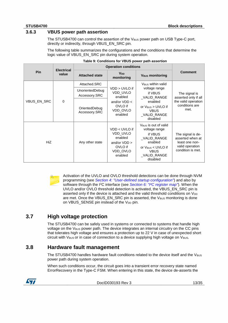
3.6.3 VBUS power path assertion
The STUSB4700 can control the assertion of the VBUS power path on USB Type-C port, directly or indirectly, through VBUS_EN_SRC pin.
The following table summarizes the configurations and the conditions that determine the logic value of VBUS_EN_SRC pin during system operation.
Table 9: Conditions for VBUS power path assertion
Pin Electrical
value
Operation conditions
Comment Attached state
VDD
monitoring VBUS monitoring
VBUS_EN_SRC 0
Attached.SRC
VDD > UVLO if
VDD_UVLO
enabled
and/or VDD <
OVLO if
VDD_OVLO
enabled
VBUS within valid
voltage range
if VBUS
_VALID_RANGE
enabled
or VBUS > UVLO if VBUS
_VALID_RANGE disabled
The signal is asserted only if all the valid operation
conditions are met.
UnorientedDebug
Accessory.SRC
OrientedDebug Accessory.SRC
HiZ Any other state
VDD < UVLO if
VDD_UVLO
enabled
and/or VDD >
OVLO if
VDD_OVLO
enabled
VBUS is out of valid voltage range
if VBUS _VALID_RANGE
enabled
or VBUS < UVLO if VBUS
_VALID_RANGE disabled
The signal is de-asserted when at
least one non-valid operation
condition is met.
Activation of the UVLO and OVLO threshold detections can be done through NVM programming (see Section 4: "User-defined startup configuration") and also by software through the I2C interface (see Section 6: "I²C register map"). When the UVLO and/or OVLO threshold detection is activated, the VBUS_EN_SRC pin is asserted only if the device is attached and the valid threshold conditions on VDD are met. Once the VBUS_EN_SRC pin is asserted, the VBUS monitoring is done on VBUS_SENSE pin instead of the VDD pin.
3.7 High voltage protection
The STUSB4700 can be safely used in systems or connected to systems that handle high voltage on the VBUS power path. The device integrates an internal circuitry on the CC pins that tolerates high voltage and ensures a protection up to 22 V in case of unexpected short circuit with VBUS or in case of connection to a device supplying high voltage on VBUS.
3.8 Hardware fault management
The STUSB4700 handles hardware fault conditions related to the device itself and the VBUS power path during system operation.
When such conditions occur, the circuit goes into a transient error recovery state named ErrorRecovery in the Type-C FSM. When entering in this state, the device de-asserts the
Block descriptions STUSB4700
14/35 DocID030193 Rev 3
VBUS power path by disabling the VBUS_EN_SRC pin, and it removes the terminations from the CC pins during several tens of milliseconds. Then, it transitions to the unattached source state.
The STUSB4700 goes into error recovery state when at least one condition listed below is met:
If an overtemperature is detected, the “THERMAL_FAULT”flag is asserted.
If an internal pull-up voltage on CC pins is below UVLO threshold, the “VPU_VALID” flag is asserted.
If an overvoltage is detected on the CC pins, the “VPU_OVP_FAULT” flag is asserted.
If the VBUS voltage is out of the valid voltage range during attachment, the “VBUS_VALID” flag is asserted.
If an undervoltage is detected on the VDD pin during attachment when UVLO detection is enabled, the “VDD_UVLO_DISABLE” flag is asserted.
If an overvoltage is detected on the VDD pin during attachment when OVLO detection is enabled, the “VDD_OVLO_DISABLE” flag is asserted.
The I2C register bits mentioned above in quotes give either the state of the hardware fault when it occurs or the setting condition to detect the hardware fault.
3.9 Accessory mode detection
The STUSB4700 supports the detection of audio accessory mode and debug accessory mode as defined in the USB Type-C standard specification source power role with accessory support.
3.9.1 Audio accessory mode detection
The STUSB4700 detects an audio accessory device when both the CC1 and CC2 pins are pulled down to ground by a Ra resistor from the connected device. The audio accessory detection is advertised through the CC_ATTACHED_MODE bits of the I2C register CC_CONNECTION_STATUS.
3.9.2 Debug accessory mode detection
The STUSB4700 detects a connection to a debug and test system (DTS) when it operates either in sink power role or source power role. The debug accessory detection is advertised by the DEBUG1 and DEBUG2 pins as well as through the CC_ATTACHED_MODE bits of the I2C register CC_CONNECTION_STATUS.
In source power role, a debug accessory device is detected when both the CC1 and CC2 pins are pulled down to ground by a Rd resistor from the connected device. The orientation detection is performed in two steps as described in the table below. The DEBUG2 pin is asserted to advertise the DTS detection and the A_B_SIDE pin indicates the orientation of the connection. The orientation detection is advertised through the TYPEC_FSM_STATE bits of the I2C register CC_OPERATION_STATUS.
STUSB4700 User-defined startup configuration
DocID030193 Rev 3 15/35
4 User-defined startup configuration
4.1 Parameter overview
The STUSB4700 has a set of user-defined parameters that can be customized by NVM re-programming and/or by software through I2C interface. It allows changing the preset configuration of USB Type-C and PD interface and to define a new configuration to meet specific customer requirements addressing various applications, use cases or specific implementations.
The NVM re-programming overrides the initial default setting to define a new default setting that will be used at power-up or after a reset. The default value is copied at power-up, or after a reset, from the embedded NVM into dedicated I2C register bits. The NVM re-programming is possible few times with a customer password.
Table 10: PDO configurations in NVM
Feature Parameter Value Default
PDO1 Voltage 5 V 5 V
Current Configurable – defined by PDO1_I [3:0] 3 A
PDO2 Voltage Configurable – defined by PDO2_V [1:0] 9 V
Current Configurable – defined by PDO2_I [3:0] 3 A
PDO3 Voltage Configurable – defined by PDO3_V [1:0] 12 V
Current Configurable – defined by PDO3_I [3:0] 3 A
PDO4 Voltage Configurable – defined by PDO4_V [1:0] 15 V
Current Configurable – defined by PDO4_I [3:0] 3 A
PDO5 Voltage Configurable – defined by PDO5_V [1:0] 20 V
Current Configurable – defined by PDO5_I [3:0] 2.25 A
When a default value is changed during system boot by software, the new settings apply as long as STUSB4700 is operating and until it is changed again. But after power-off and power-up, or after a hardware reset, STUSB4700 takes back default values defined in the NVM.
4.2 PDO – voltage configuration in NVM
PDO2_V [1:0], PDO3_V [1:0], PDO4_V [1:0] and PDO5_V [1:0] can be configured with the following values:
Table 11: PDO NVM voltage configuration
Value Configuration
2b00 9 V
2b01 15 V
2b10 PDO_FLEX_V1
2b11 PDO_FLEX_V2
PDO_FLEX_V1 and PDO_FLEX_V2 are defined in a specific 10-bit register, value being expressed in 50 mV units.
User-defined startup configuration STUSB4700
16/35 DocID030193 Rev 3
For instance:
PDO_FLEX_V1 = 10b0100100010 → 14.5 V
PDO_FLEX_V2 = 10b0110000110 → 19.5 V
4.3 PDO – current configuration in NVM
PDO1_I [3:0], PDO2_I [3:0], PDO3_I [3:0], PDO4_I [3:0] and PDO5_I [3:0] can be configured with the following fixed values:
Table 12: PDO NVM current configuration
Value Configuration
4b0000 PDO_FLEX_I
4b0001 1.50 A
4b0010 1.75 A
4b0011 2.00 A
4b0100 2.25 A
4b0101 2.50 A
4b0110 2.75 A
4b0111 3.00 A
4b1000 3.25 A
4b1001 3.50 A
4b1010 3.75 A
4b1011 4.00 A
4b1100 4.25 A
4b1101 4.50 A
4b1110 4.75 A
4b1111 5.00 A
PDO_FLEX_I is defined in a specific 10-bit register, value being expressed in 10 mA units. For instance:
PDO_FLEX_I = 10b0011100001 → 2.25 A
4.4 Monitoring configuration in NVM
T_PDO_Transition can be configured from 20 to 300 ms by increments of 20 ms (0 is not recommended)
T_Transition_to_0V can be configured from 84 to 1260 ms by increments of 84 ms (0 is not recommended)
Vshift_High can be configured from (5 to 20%)
Vshift _Low can be configured from (5 to 20%)
4.5 Discharge configuration in NVM
Enable discharge
Internal discharge
Reverse
STUSB4700 I²C interface
DocID030193 Rev 3 17/35
5 I²C interface
5.1 Read and write operations
The I²C interface is used to configure, control and read the status of the device. It is compatible with the Philips I²C Bus® (version 2.1). The I²C is a slave serial interface based on two signals:
SCL - serial clock line: input clock used to shift data
SDA - serial data line: input/output bidirectional data transfers
A filter rejects the potential spikes on the bus data line to preserve data integrity.
The bidirectional data line supports transfers up to 400 Kbit/s (fast mode). The data are shifted to and from the chip on the SDA line, MSB first.
The first bit must be high (START) followed by the 7-bit device address and the read/write control bit.
Eigth two 7-bit device addresses are available for STUSB4700 thanks to external programming of DevADDR0, DevADDR11 and/or DevADDR2 through ADDR0, ADDR1/ADDR2 pin setting. It allows to connect two up to 8 STUSB4700 devices on the same I2C bus.
ADDR are not available for all configurations.
Device address format:
Bit7 Bit6 Bit5 Bit4 Bit3 Bit2 Bit1 Bit0
DevADDR6 DevADDR5 DevADDR4 DevADDR3 DevADDR2 DevADDR1 DevADDR0 R/W
0 1 0 1 ADDR2 ADDR1 ADDR0 0/1
Register address format:
Bit7 Bit6 Bit5 Bit4 Bit3 Bit2 Bit1 Bit0
RegADDR7 RegADDR6 RegADDR5 RegADDR4 RegADDR3 RegADDR2 RegADDR1 RegADDR0
Register data format:
Bit7 Bit6 Bit5 Bit4 Bit3 Bit2 Bit1 Bit0
DATA7 DATA6 DATA5 DATA4 DATA3 DATA2 DATA1 DATA0

I²C interface STUSB4700
18/35 DocID030193 Rev 3
Figure 3: Read operation
Figure 4: Write operation
5.2 Timing specifications
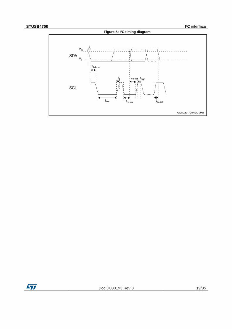
The device uses a standard slave I²C channel at speed up to 400 kHz.
Table 13: I2C timing parameters - VDD = 5 V
Symbol Parameter Min Typ Max Unit
Fscl SCL clock frequency 0 - 400 kHz
thd,sta Hold time (repeated) START condition 0.6 - - µs
tlow LOW period of the SCL clock 1.3 - - µs
thigh HIGH period of the SCL clock 0.6 - - µs
tsu,dat Setup time for repeated START condition 0.6 - - µs
thd,dat Data hold time 0.04 - 0.9 µs
tsu,dat Data setup time 100 - - µs
tr Rise time of both SDA and SCL signals 20 + 0.1 Cb - 300 ns
tf Fall time of both SDA and SCL signals 20 + 0.1 Cb - 300 ns
tsu,sto Setup time for STOP condition 0.6 - - µs
tbuf Bus free time between a STOP and START condition 1.3 - - µs
Cb Capacitive load for each bus line - - 400 pF
STUSB4700 I²C interface
DocID030193 Rev 3 19/35
Figure 5: I²C timing diagram
I²C register map STUSB4700
20/35 DocID030193 Rev 3
6 I²C register map Table 14: STUSB4700 register map overview
Address Register name Access Description
00h
to
0Ah
Reserved RO Do not use
0Bh ALERT_STATUS RC Alert register linked to transition registers
0Ch ALERT_STATUS_MASK_CTRL R/W Interrupt mask on ALERT_STATUS register
0Dh CC_CONNECTION_STATUS_TRANS RC Alerts on transition in CC_CONNECTION_STATUS
register
0Eh CC_CONNECTION_STATUS RO CC connection status
0Fh MONITORING_STATUS_TRANS RC Alerts on transition in MONITORING_STATUS
register
10h MONITORING_STATUS RO Gives status on VBUS voltage monitoring
11h Reserved RO Do not use
12h HW_FAULT_STATUS_TRANS RC Alerts on transition in HW_FAULT_STATUS
register
13h HW_FAULT_STATUS RO Hardware faults status
14h
to
17h
Reserved RO Do not use
18h CC_CAPABILITY_CTRL R/W Allows to change the CC capabilities
19h
to
22h
Reserved RO Do not use
23h RESET_CTRL R/W Controls the device reset by software
24h Reserved RO Do not use
25h VBUS_DISCHARGE_TIME_CTRL R/W Parameters defining VBUS discharge time
26h VBUS_DISCHARGE_CTRL R/W Controls the VBUS discharge path
27h VBUS_ENABLE_STATUS RO VBUS power path activation status
2Eh VBUS_MONITORING_CTRL R/W Allows to change the monitoring conditions of VBUS
voltage
19h
to
1Eh
Reserved RO Do not use
71h SRC_PDO1 R/W PDO1 capabilities configuration
75h SRC_PDO2 R/W PDO2 capabilities configuration
79h SRC_PDO3 R/W PDO3 capabilities configuration
7Dh SRC_PDO4 R/W PDO4 capabilities configuration
81h SRC_PDO5 R/W PDO5 capabilities configuration
91h SRC_RDO RO PDO request status
STUSB4700 I²C register map
DocID030193 Rev 3 21/35
Table 15: Register access legend
Access code Expanded name Description
RO Read only Register can be read only
R/W Read / Write Register can be read or written
RC Read and clear Register can be read and is cleared after read
Typical use cases STUSB4700
22/35 DocID030193 Rev 3
7 Typical use cases
7.1 Power supply – buck topology
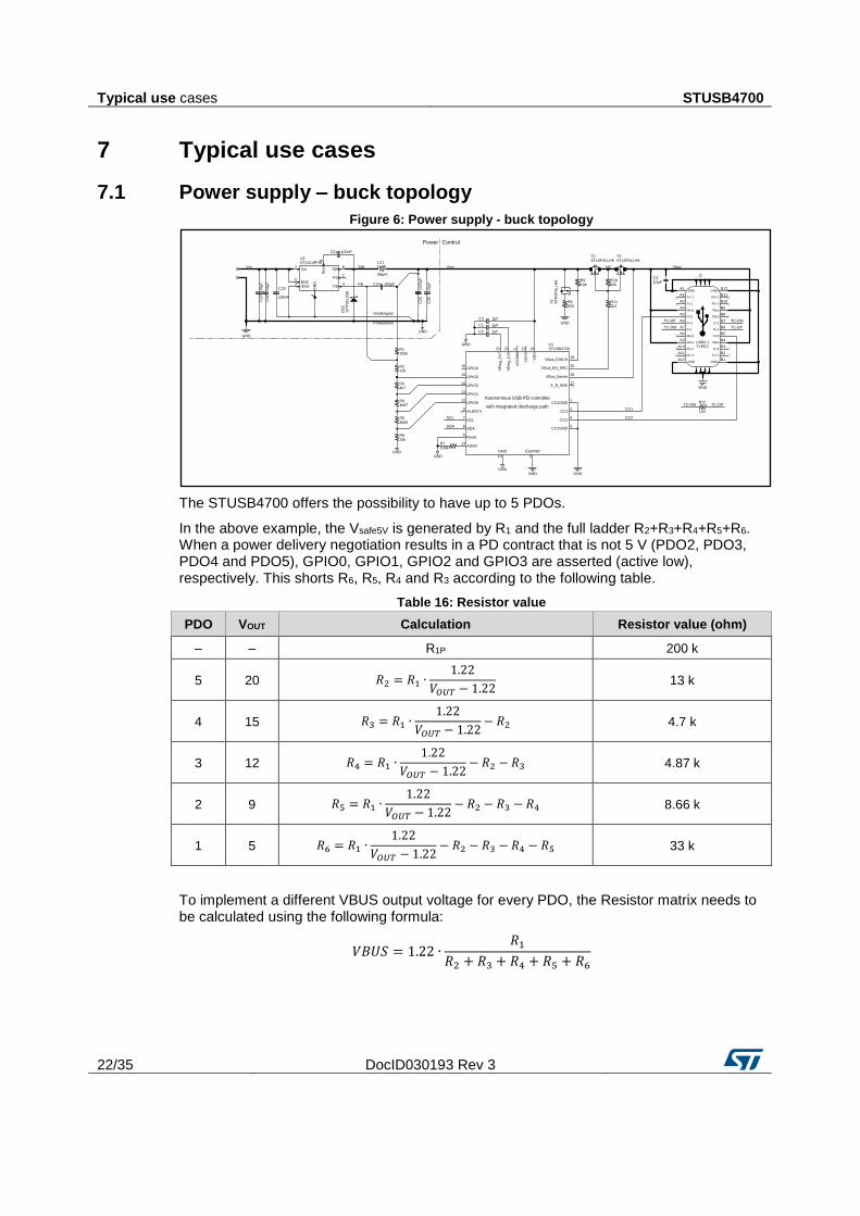
Figure 6: Power supply - buck topology
The STUSB4700 offers the possibility to have up to 5 PDOs.
In the above example, the Vsafe5V is generated by R1 and the full ladder R2+R3+R4+R5+R6. When a power delivery negotiation results in a PD contract that is not 5 V (PDO2, PDO3, PDO4 and PDO5), GPIO0, GPIO1, GPIO2 and GPIO3 are asserted (active low), respectively. This shorts R6, R5, R4 and R3 according to the following table.
Table 16: Resistor value
PDO VOUT Calculation Resistor value (ohm)
– – R1P 200 k
5 20 𝑅2 = 𝑅1 ∙1.22
𝑉𝑂𝑈𝑇 − 1.22 13 k
4 15 𝑅3 = 𝑅1 ∙1.22
𝑉𝑂𝑈𝑇 − 1.22− 𝑅2 4.7 k
3 12 𝑅4 = 𝑅1 ∙1.22
𝑉𝑂𝑈𝑇 − 1.22− 𝑅2 − 𝑅3 4.87 k
2 9 𝑅5 = 𝑅1 ∙1.22
𝑉𝑂𝑈𝑇 − 1.22− 𝑅2 − 𝑅3 − 𝑅4 8.66 k
1 5 𝑅6 = 𝑅1 ∙1.22
𝑉𝑂𝑈𝑇 − 1.22− 𝑅2 − 𝑅3 − 𝑅4 − 𝑅5 33 k
To implement a different VBUS output voltage for every PDO, the Resistor matrix needs to be calculated using the following formula:
𝑉𝐵𝑈𝑆 = 1.22 ∙𝑅1
𝑅2 + 𝑅3 + 𝑅4 + 𝑅5 + 𝑅6
4k7
B8Sbu2
22
C21 100nF
GND
VS
YS
CC1
1
68µH
Vbus
GN
D
CC2
2
Rx+1
B10
TC-DP
TC-DPCC1GND
14
15
10µF
Tx+2
EN2
C1
R3
GND
SW
Tx-1
Vbus
Control
8k66
1µF
A3
TC-DM
100
T1
SDA
GNDB1
10µ
F
8SW
B12C23
3
R11
B2
D-1
GPIO1
GND
R7
A4
HC
FB
Smallsignal
Vin
A11
R4
TC-DP
GND
33k13
B6
A12
2k2
GND
C2
T3
3
A6
R2
VBus_Sense
9
C4
24
R5
VD
D
T2
A10
SCL
820
Rx+2
6
R6
Vin
12
11
GND
/EN1
Autonomous USB PD controller
with integrated discharge path
19
SCL
8
D-2
200k
1µF
A5
10µ
F
GND
CC1
Rx-2STUSB4700
5
R12
+
R1
VR
eg
_1
V2
GND
Vbus
CC2
VBus_DISCH
4FB
18
CC1
TYPEC
J1
USB3.1
PG2
ST
R2
P3
LL
H6
4k87
100k
CC2
Vbus
Power
ST1S14PHR
GND
Reset
GND
10
7
ST
PS
5L
25
B
B11
Vsrc
C3
5
0
ExpPAD
U1
B5
21
10k
20VBus_EN_SRC
17
D+1
23
D+2
Vbus
Rx-1
VR
eg
_2
V7
STL6P3LLH6
GND
GND
Bo
ot
22
0µ
F
A9Sbu1
U2
GNDC3
C2
5
R10
TC-DM
D2
1
16
6
B9
GND
STL6P3LLH6
Tx-2
10k
C3
2
SDA
5
Powerplane
R9
A7
A8
13k
R8
Tx+1
B7
A2
CC2GND
4
10µ
F
L21
C24 100pF
220nF
VC
ON
N
1
GPIO3
C2
2
B3
B4
A1
A_B_Side
7
1µFTC-DM
GPIO2
GPIO0
ALERT#
Addr0
GPIO4
STUSB4700 Typical use cases
DocID030193 Rev 3 23/35
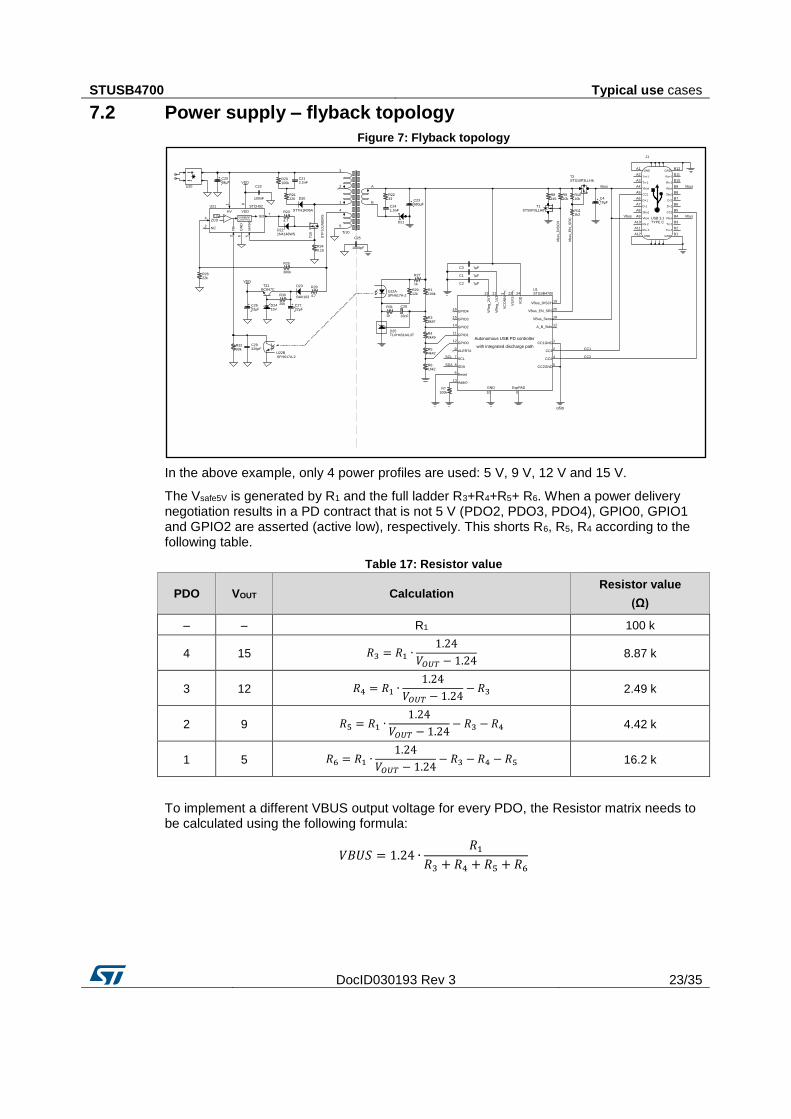
7.2 Power supply – flyback topology
Figure 7: Flyback topology
In the above example, only 4 power profiles are used: 5 V, 9 V, 12 V and 15 V.
The Vsafe5V is generated by R1 and the full ladder R3+R4+R5+ R6. When a power delivery negotiation results in a PD contract that is not 5 V (PDO2, PDO3, PDO4), GPIO0, GPIO1 and GPIO2 are asserted (active low), respectively. This shorts R6, R5, R4 according to the following table.
Table 17: Resistor value
PDO VOUT Calculation Resistor value
(Ω)
– – R1 100 k
4 15 𝑅3 = 𝑅1 ∙1.24
𝑉𝑂𝑈𝑇 − 1.24 8.87 k
3 12 𝑅4 = 𝑅1 ∙1.24
𝑉𝑂𝑈𝑇 − 1.24− 𝑅3 2.49 k
2 9 𝑅5 = 𝑅1 ∙1.24
𝑉𝑂𝑈𝑇 − 1.24− 𝑅3 − 𝑅4 4.42 k
1 5 𝑅6 = 𝑅1 ∙1.24
𝑉𝑂𝑈𝑇 − 1.24− 𝑅3 − 𝑅4 − 𝑅5 16.2 k
To implement a different VBUS output voltage for every PDO, the Resistor matrix needs to be calculated using the following formula:
𝑉𝐵𝑈𝑆 = 1.24 ∙𝑅1
𝑅3 + 𝑅4 + 𝑅5 + 𝑅6
1µF
D25
33nF
GND
100k
T21
TYPE C
R29
R25
B6
R26
CC2
2
R10
Vbus
Rx-2
A12
5
U21
+
R21
R11
VR
eg_2V
7
21
R3
USB 3.1
3
VBus_DISCH
T2
22µF
B8
B12
D+2
B
B1
2.5V
A1
1.5nF
GND
100nF
HV
10µF
SFH617A-2
SDA
1k5D-2
A6 B7
D23
SCL
8
A11
133
R7
STS10P3LLH6
24
C29
STTH1R06A
CC1
1
U22A
GND
Tx+2
100k
B2
360k
R1
15V
A
GND
A5
C3
ZCD
1
Vbus
R8
GPIO3
16
Tr20
A_B_Side
7
+
R30
C26
Reset
GND
A7
B11
R27
1k
T20
BAV103
CC1GND
BC847C
3
8k87
Rx-1
sense
6
D212
NC5
R23
4
T1
VDD
GPIO4
6
C1
+
CC2
C27
STS5P3LLH6
U20
Rx+1R20 B10
R28
10k
220pF
Rx+2
A4 B9
+
+
SCL
D-1
4
4.7
GD7
14GPIO2
15
Vbus
C25
680µF
VDD
22
VS
YS
VD
D
0
U1
ExpPAD
R22
1µF
Vbus
R4
SDA
VDD
30k
R24
8
22k
3F
B
1000pF
+
C21
Sbu2
Vbus
C24
16k2
10
5
A8
A9
12GPIO0
11
22µF
18VBus_Sense
9ALERT#
2k2
VR
eg_1V
2
R31
1k
R5
GPIO1
B3
~-
4k42
Tx-2
R32
-CURRENT
TLVH431AIL3T
C28
CC1
GN
D
STCH02
SFH617A-2
A2
Sbu1
220
CC2GND
4
CC1
2
Tx+1
Vb
us_D
ISC
H
R6
2k49
D22
Vbus
ST
F10
LN
80K
5 B4
13Addr0
STUSB4700
0.15
Vbus
Autonomous USB PD controller
with integrated discharge path
100k
CONTROLVbus
C2
Vb
us_E
N_S
RC
19
C23
GND
12k
Tx-1A3
10k
A10
C4
C22
VC
ON
N
D+1
2.2nF
J1
R9
1µF
23
20VBus_EN_SRC
17
D24 20k
U22B
CC2
1N4148WS
D20
B5
~+
4.7
C2068µF

Electrical characteristics STUSB4700
24/35 DocID030193 Rev 3
8 Electrical characteristics
8.1 Absolute maximum rating
All voltages are referenced to GND.
Table 18: Absolute maximum rating
Symbol Parameter Value Unit
VDD Supply voltage 28 V
VSYS Supply voltage on VSYS pin 6 V
VCC1, VCC2 High voltage on CC pins 22 V
VVBUS_EN_SRC
VVBUS_SENSE High voltage on VBUS pins 28 V
VSCL, VSDA
VALERT#
VRESET
VA_B_SIDE
Operating voltage on I/O pins -0.3 to 6 V
VCONN VCONN voltage 6 V
TSTG Storage temperature -55 to 150 °C
TJ Maximum junction temperature 145 °C
ESD HBM 4
kV CDM 1.5
8.2 Operating conditions
Table 19: Operating conditions
Symbol Parameter Value Unit
VDD Supply voltage 4.1 to 22 V
VSYS Supply voltage on VSYS pin 3.0 to 5.5 V
VCC1, VCC2 CC pins (1) -0.3 to 5.5 V
VVBUS_EN_SRC
VVBUS_DISCH
VVBUS_SENSE
High voltage pins 0 to 22 V
VSCL, VSDA
VALERT#
VRESET
VA_B_SIDE
Operating voltage on I/O pins 0 to 4.5 V
VCONN VCONN voltage 2.7 to 5.5 V
ICONN VCONN rated current (default = 0.35 A) 0.1 to 0.6 A
TA Operating temperature -40 to 105 °C
Notes:
(1)Transient voltage on CC1 and CC2 pins are allowed to go down to -0.3 during BMC communication from
STUSB4700 Electrical characteristics
DocID030193 Rev 3 25/35
connected devices.
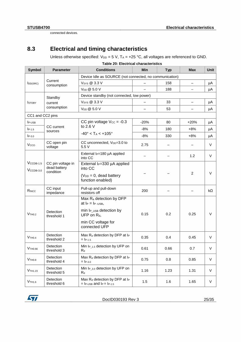
8.3 Electrical and timing characteristics
Unless otherwise specified: VDD = 5 V, TA = +25 °C, all voltages are referenced to GND.
Table 20: Electrical characteristics
Symbol Parameter Conditions Min Typ Max Unit
IDD(SRC) Current
consumption
Device Idle as SOURCE (not connected, no communication)
VSYS @ 3.3 V – 158 – µA
VDD @ 5.0 V – 188 – µA
ISTDBY
Standby
current
consumption
Device standby (not connected, low power)
VSYS @ 3.3 V – 33 – µA
VDD @ 5.0 V – 53 – µA
CC1 and CC2 pins
IP-USB
CC current sources
CC pin voltage VCC = -0.3 to 2.6 V
-40° < TA < +105°
-20% 80 +20% µA
IP-1.5 -8% 180 +8% µA
IP-3.0 -8% 330 +8% µA
VCCO CC open pin voltage
CC unconnected, VDD=3.0 to 5.5 V
2.75 – – V
VCCDB-1.5
VCCDB-3.0
CC pin voltage in dead battery condition
External IP=180 µA applied into CC
– – 1.2 V
External IP=330 µA applied into CC
(VDD = 0, dead battery function enabled)
– – 2 V
RINCC CC input impedance
Pull-up and pull-down resistors off
200 – – kΩ
VTH0.2 Detection threshold 1
Max Ra detection by DFP at IP = IP -USB,
min IP_USB detection by UFP on Rd,
min CC voltage for connected UFP
0.15 0.2 0.25 V
VTH0.4 Detection threshold 2
Max Ra detection by DFP at IP
= IP-1.5 0.35 0.4 0.45 V
VTH0.66 Detection threshold 3
Min IP_1.5 detection by UFP on Rd
0.61 0.66 0.7 V
VTH0.8 Detection threshold 4
Max Ra detection by DFP at IP = IP-3.0
0.75 0.8 0.85 V
VTH1.23 Detection threshold 5
Min IP_3.0 detection by UFP on Rd
1.16 1.23 1.31 V
VTH1.6 Detection threshold 6
Max Rd detection by DFP at IP = IP-USB and IP = IP-1.5
1.5 1.6 1.65 V
Electrical characteristics STUSB4700
26/35 DocID030193 Rev 3
Symbol Parameter Conditions Min Typ Max Unit
VTH2.6 Detection threshold 7
Max Rd detection by DFP at IP-3.0,
max CC voltage for connected UFP
2.45 2.6 2.75 V
VCONN protection
RVCONN VCONN path
resistance
IVCONN = 0.2 A
-40°C < TA < +105°C 0.25 0.5 0.975 Ω
IOCP Over current protection
Programmable current limit
threshold (from 100 mA to 600
mA by step of 50 mA).
85 100 125
mA 300 350 400
550 600 650
VOVP Output over
voltage protection 5.9 6 6.1 V
VUVP Input under
voltage protection
Low UVLO threshold 2.6 – 2.7 V
High UVLO threshold (default) 4.6 – 4.8
VBUS monitoring and driving
VTHUSB VBUS presence threshold
VSYS=3.0 to 5.5 V 3.8 3.9 4 V
VTH0V VBUS safe 0V threshold (vSafe0V)
VSYS=3.0 to 5.5 V
Programmable threshold
(from 0.6 to 1.8 V)
Default VTHOV= 0.6 V
0.5 0.6 0.7
V
0.8 0.9 1
1.1 1.2 1.3
1.7 1.8 1.9
RDISUSB VBUS discharge resistor
600 700 800 Ω
TDISUSB VBUS discharge time to 0 V
Default TDISUSB= 840 ms . The coefficient TDISPARAM is programmable by NVM.
70
*TDISPARAM
84
*TDISPARAM
100
*TDISPARAM ms
TDISUSB VBUS discharge time to PDO
Default TDISUSB= 200 ms
The coefficient TDISPARAM is programmable by NVM
20
*TDISPARAM
24
*TDISPARAM
28
*TDISPARAM ms
VMONUSBH VBUS monitoring high voltage threshold
VBUS = nominal target value
Default VMONUSBH = VBUS
+10%
The threshold limit is programmable by NVM from VBUS +5% to VBUS +20%
– VBUS +10% – V
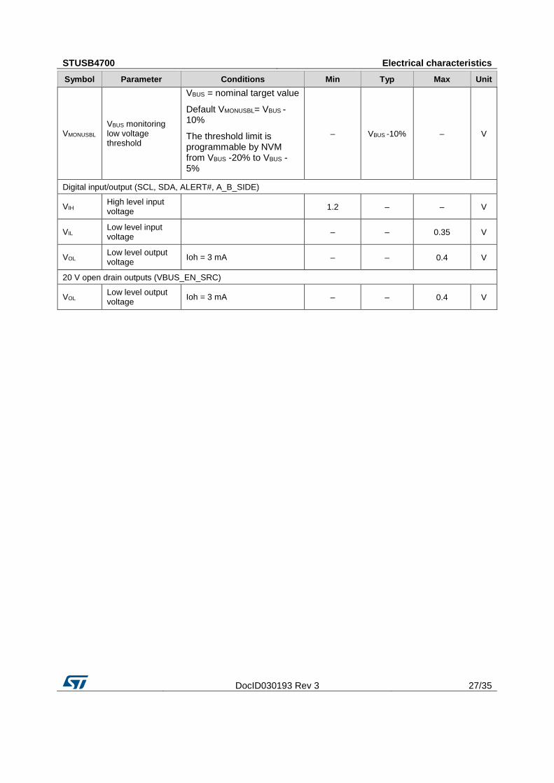
STUSB4700 Electrical characteristics
DocID030193 Rev 3 27/35
Symbol Parameter Conditions Min Typ Max Unit
VMONUSBL VBUS monitoring low voltage threshold
VBUS = nominal target value
Default VMONUSBL= VBUS -10%
The threshold limit is programmable by NVM from VBUS -20% to VBUS -5%
– VBUS -10% – V
Digital input/output (SCL, SDA, ALERT#, A_B_SIDE)
VIH High level input voltage
1.2 – – V
VIL Low level input voltage
– – 0.35 V
VOL Low level output voltage
Ioh = 3 mA – – 0.4 V
20 V open drain outputs (VBUS_EN_SRC)
VOL Low level output voltage
Ioh = 3 mA – – 0.4 V
Package information STUSB4700
28/35 DocID030193 Rev 3
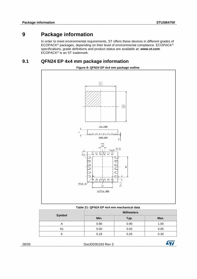
9 Package information
In order to meet environmental requirements, ST offers these devices in different grades of ECOPACK® packages, depending on their level of environmental compliance. ECOPACK® specifications, grade definitions and product status are available at: www.st.com. ECOPACK® is an ST trademark.
9.1 QFN24 EP 4x4 mm package information
Figure 8: QFN24 EP 4x4 mm package outline
Table 21: QFN24 EP 4x4 mm mechanical data
Symbol Millimeters
Min. Typ. Max.
A 0.80 0.90 1.00
A1 0.00 0.02 0.05
b 0.18 0.25 0.30
STUSB4700 Package information
DocID030193 Rev 3 29/35
Symbol Millimeters
Min. Typ. Max.
D 3.95 4.00 4.05
D2 2.55 2.70 2.80
E 3.95 4.00 4.05
E2 2.55 2.70 2.80
e 0.45 0.50 0.55
K 0.15 — —
L 0.30 0.40 0.50
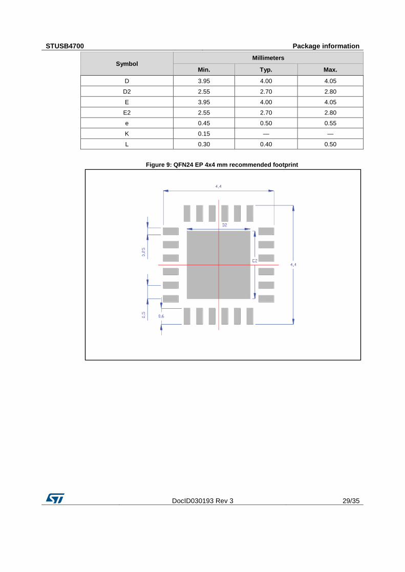
Figure 9: QFN24 EP 4x4 mm recommended footprint
Package information STUSB4700
30/35 DocID030193 Rev 3
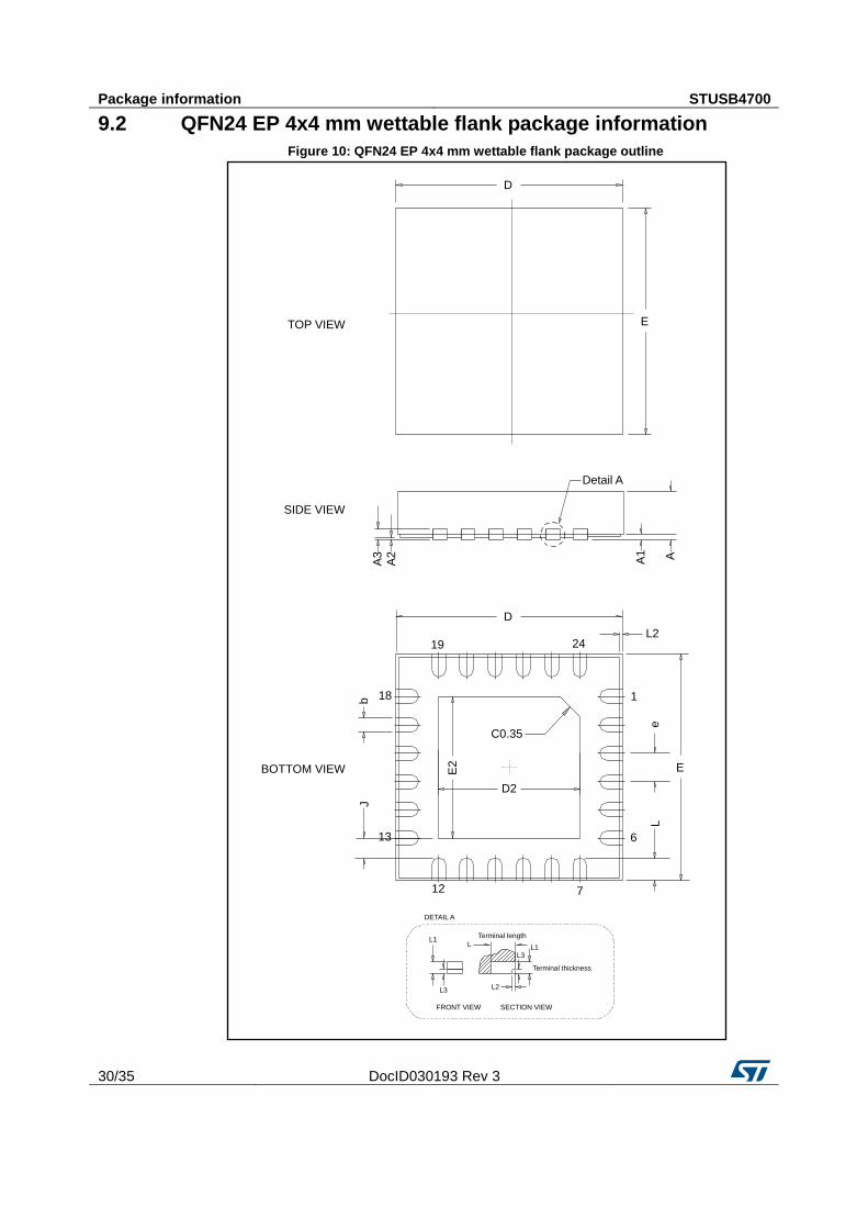
9.2 QFN24 EP 4x4 mm wettable flank package information
Figure 10: QFN24 EP 4x4 mm wettable flank package outline
D
ETOP VIEW
AA1
SIDE VIEW
A2
A3
Detail A
D2
E2
C0.35
19 24
1
6
712
D
L2
18
13
Jb
Le
EBOTTOM VIEW
FRONT VIEW SECTION VIEW
Terminal thickness
Terminal lengthL1
L3 L2
L3L1L
DETAIL A
STUSB4700 Package information
DocID030193 Rev 3 31/35
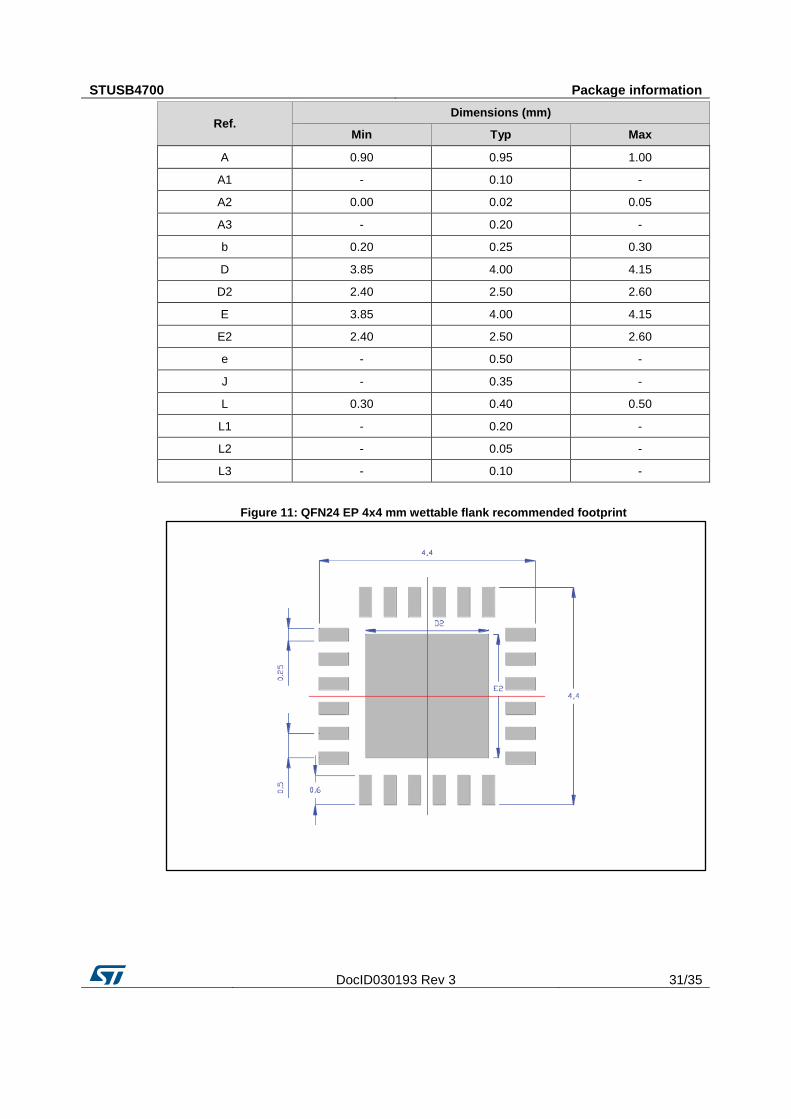
Ref. Dimensions (mm)
Min Typ Max
A 0.90 0.95 1.00
A1 - 0.10 -
A2 0.00 0.02 0.05
A3 - 0.20 -
b 0.20 0.25 0.30
D 3.85 4.00 4.15
D2 2.40 2.50 2.60
E 3.85 4.00 4.15
E2 2.40 2.50 2.60
e - 0.50 -
J - 0.35 -
L 0.30 0.40 0.50
L1 - 0.20 -
L2 - 0.05 -
L3 - 0.10 -
Figure 11: QFN24 EP 4x4 mm wettable flank recommended footprint
Package information STUSB4700
32/35 DocID030193 Rev 3
9.3 Thermal information
Table 22: Thermal information
Symbol Parameter Value Unit
RθJA Junction-to-ambient thermal resistance 37 °C/W
RθJC Junction-to-case thermal resistance 5
9.4 Packing information
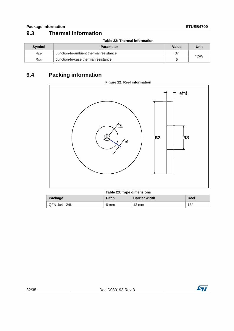
Figure 12: Reel information
Table 23: Tape dimensions
Package Pitch Carrier width Reel
QFN 4x4 - 24L 8 mm 12 mm 13"
STUSB4700 Terms and abbreviations
DocID030193 Rev 3 33/35
10 Terms and abbreviations Table 24: List of terms and abbreviations
Term Description
Accessory
modes
Audio adapter accessory mode. It is defined by the presence of Ra/Ra on the
CC1/CC2 pins.
Debug accessory mode. It is defined by the presence of Rd/Rd on CC1/CC2 pins in
Source power role or Rp/Rp on CC1/CC2 pins in Sink power role.
DFP
Downstream Facing Port, associated with the flow of data in a USB connection.
Typically, the ports on a HOST or the ports on a hub to which devices are connected.
In its initial state, the DFP sources VBUS and VCONN and supports data.
DRP Dual-role port. A port that can operate as either a source or a sink. The port's role
may be changed dynamically.
Sink Port asserting Rd on the CC pins and consuming power from the VBUS; most
commonly a device.
Source Port asserting Rp on the CC pins and providing power over the VBUS; usually a host or
hub DFP.
UFP
Upstream Facing Port, specifically associated with the flow of data in a USB
connection. The port on a device or a hub that connects to a host or the DFP of a
hub. In its initial state, the UFP sinks the VBUS and supports data.
Revision history STUSB4700
34/35 DocID030193 Rev 3
11 Revision history Table 25: Document revision history
Date Version Changes
24-Jan-2017 1 Initial release.
22-Mar-2017 2
Updated comments columns in Table 7: "GPIO1 (pin #11) configuration" and Table 8: "GPIO2 (pin #14) – GPIO3 (pin #15) – GPIO4 (pin #16) configuration", and ESD parameter description in Table 18: "Absolute maximum rating".
In Table 19: "Operating conditions " replaced VVBUS_EN_SNK with VVBUS_DISCH. Replaced Figure 6: "Power supply - buck topology" with a new figure. Minor changes throughout the document.
06-Dec-2017 3
On cover page:
- updated title description
- updated feature regarding protections
- added feature regarding Automotive grade availability
- updated feature regarding Certification test ID
- updated Table 1: "Device summary table"
Updated Section 7.1: "Power supply – buck topology"
Updated Section 7.2: "Power supply – flyback topology"
Added Section 9.2: "QFN24 EP 4x4 mm wettable flank package information"
STUSB4700
DocID030193 Rev 3 35/35
IMPORTANT NOTICE – PLEASE READ CAREFULLY
STMicroelectronics NV and its subsidiaries (“ST”) reserve the right to make changes, corrections, enhancements, modifications , and improvements to ST products and/or to this document at any time without notice. Purchasers should obtain the latest relevant information on ST products before placing orders. ST products are sold pursuant to ST’s terms and conditions of sale in place at the time of order acknowledgement.
Purchasers are solely responsible for the choice, selection, and use of ST products and ST assumes no liability for application assistance or the design of Purchasers’ products.
No license, express or implied, to any intellectual property right is granted by ST herein.
Resale of ST products with provisions different from the information set forth herein shall void any warranty granted by ST for such product.
ST and the ST logo are trademarks of ST. All other product or service names are the property of their respective owners.
Information in this document supersedes and replaces information previously supplied in any prior versions of this document.
© 2017 STMicroelectronics – All rights reserved