Automotive Advanced Secondary Side LLC Resonant Converter ...
30
DATA SHEET www. onsemi.com © Semiconductor Components Industries, LLC, 2020 November, 2021 − Rev. 2 1 Publication Order Number: NCV4390/D Automotive Advanced Secondary Side LLC Resonant Converter Controller with Synchronous Rectifier Control NCV4390 The NCV4390 is an advanced Pulse Frequency Modulated (PFM) controller for LLC resonant converters with Synchronous Rectification (SR) that offers best in class efficiency for isolated DC/DC converters. It employs a current mode control technique based on a charge control, where the triangular waveform from the oscillator is combined with the integrated switch current information to determine the switching frequency. This provides a better control−to−output transfer function of the power stage simplifying the feedback loop design while allowing true input power limit capability. Closed−loop soft−start prevents saturation of the error amplifier and allows monotonic rising of the output voltage regardless of load condition. A dual edge tracking adaptive dead time control minimizes the body diode conduction time thus maximizing efficiency. Features • Secondary Side PFM Controller for LLC Resonant Converter with Synchronous Rectifier Control • Charge Current Control for Better Transient Response and Easy Feedback Loop Design • Adaptive Synchronous Rectification Control with Dual Edge Tracking • Closed Loop Soft−Start for Monotonic Rising Output • Wide Operating Frequency (39 kHz ~ 690 kHz) • Green Functions to Improve Light−Load Efficiency ♦ Symmetric PWM Control at Light−Load to Limit the Switching Frequency while Reducing Switching Losses ♦ Disabling SR at Light−Load Condition • Protection Functions with Auto−Restart ♦ Over−Current Protection (OCP) ♦ Output Short Protection (OSP) ♦ NON Zero−Voltage Switching Prevention (NZS) by Compensation Cutback (Frequency Shift) ♦ Power Limit by Compensation Cutback (Frequency Shift) ♦ Overload Protection (OLP) • Programmable Dead Times for Primary Side Switches and Secondary Side Synchronous Rectifiers • V DD Under−Voltage Lockout (UVLO) • Wide Operating Temperature Range −40°C to +125°C • Automotive Qualified to AEC−Q100 Grade 1 • This Device is Pb−Free, Halogen Free/BFR Free and is RoHS Compliant Applications • Automotive On Board Charger • EV High Voltage DC/DC Converters See detailed ordering and shipping information on page 3 of this data sheet. ORDERING INFORMATION MARKING DIAGRAM SOIC−16 CASE 751B−05 PIN CONNECTIONS NCV4390 = Specific Device Code A = Assembly Location L = Wafer Lot Y = Year WW = Work Week G = Pb−Free Package 1 1 10 11 14 15 16 2 3 4 5 6 7 8 9 12 13 PROUT1 PROUT2 ICS RDT FMIN COMP GND VDD SROUT1 SR1DS SROUT2 SS CS FB 5VB PWMS NCV4390 AWLYWWG
Transcript of Automotive Advanced Secondary Side LLC Resonant Converter ...

DATA SHEETwww.onsemi.com
© Semiconductor Components Industries, LLC, 2020
November, 2021 − Rev. 21 Publication Order Number:
NCV4390/D
Automotive AdvancedSecondary Side LLCResonant Converter Controllerwith Synchronous RectifierControlNCV4390
The NCV4390 is an advanced Pulse Frequency Modulated (PFM)controller for LLC resonant converters with SynchronousRectification (SR) that offers best in class efficiency for isolatedDC/DC converters. It employs a current mode control technique basedon a charge control, where the triangular waveform from the oscillatoris combined with the integrated switch current information todetermine the switching frequency. This provides a bettercontrol−to−output transfer function of the power stage simplifying thefeedback loop design while allowing true input power limit capability.Closed−loop soft−start prevents saturation of the error amplifier andallows monotonic rising of the output voltage regardless of loadcondition. A dual edge tracking adaptive dead time control minimizesthe body diode conduction time thus maximizing efficiency.Features• Secondary Side PFM Controller for LLC Resonant Converter with
Synchronous Rectifier Control• Charge Current Control for Better Transient Response and Easy
Feedback Loop Design• Adaptive Synchronous Rectification Control with Dual Edge
Tracking• Closed Loop Soft−Start for Monotonic Rising Output
• Wide Operating Frequency (39 kHz ~ 690 kHz)
• Green Functions to Improve Light−Load Efficiency♦ Symmetric PWM Control at Light−Load to Limit the Switching
Frequency while Reducing Switching Losses♦ Disabling SR at Light−Load Condition
• Protection Functions with Auto−Restart♦ Over−Current Protection (OCP)♦ Output Short Protection (OSP)♦ NON Zero−Voltage Switching Prevention (NZS) by
Compensation Cutback (Frequency Shift)♦ Power Limit by Compensation Cutback (Frequency Shift)♦ Overload Protection (OLP)
• Programmable Dead Times for Primary Side Switches and SecondarySide Synchronous Rectifiers
• VDD Under−Voltage Lockout (UVLO)
• Wide Operating Temperature Range −40°C to +125°C
• Automotive Qualified to AEC−Q100 Grade 1
• This Device is Pb−Free, Halogen Free/BFR Free and is RoHSCompliant
Applications• Automotive On Board Charger
• EV High Voltage DC/DC Converters
See detailed ordering and shipping information on page 3 ofthis data sheet.
ORDERING INFORMATION
MARKING DIAGRAM
SOIC−16CASE 751B−05
PIN CONNECTIONS
NCV4390 = Specific Device CodeA = Assembly LocationL = Wafer LotY = YearWW = Work WeekG = Pb−Free Package
1
1
10
11
14
15
16
2
3
4
5
6
7
8 9
12
13
PROUT1
PROUT2
ICS
RDT
FMIN
COMP
GND
VDD
SROUT1
SR1DS
SROUT2SS
CS
FB
5VB
PWMS
NCV4390AWLYWWG

NCV4390
www.onsemi.com2
Figure 1. Typical Application Schematic of NCV4390
VO
5VB
CS RDT
FMIN
ICS
SS
COMP
FB
GND
VDD
PROUT1
PROUT2
SROUT1
SROUT2
SR1DS
PWMS
PRDRV+
PRDRV−
SRDRV1
SRDRV2
SRDRV2
SRDRV1
Q1
Q2
VIN
PRDRV+
PRDRV−
SR1
SR2
COUT
RSRDS1 RSRDS2
CVDD
RDT
CDT
CSS
CICS
CCOMP
RFMIN
RPWMS
C5VB
RICS
RCS1
RCS2
CR
CT
Np
Ns
Ns
RGS1
RGS2
RG1
RG2
DG2
DG1
CIN
RFB1
R
Block Diagram
Figure 2. Internal Block Diagram of NCV4390
5VB
PWMS
FMIN
SS
ICS
CS
RDT
SR1DS
SROUT1
SROUT2
PROUT1
PROUT2
VDD
GND
Dual Edge AdaptiveTracking SR Control Block
SR Conduction DetectBlock
SR1_CND SR2_CND
SR STOP
ICS_RSTCurrent
Analyzer
CompensationCutback signal
Generator
+
−
1.5V
1V
VCT
CT_RST
3/4
DigitalPFM/PWM
Block
Dead TimeControlBlock
SKIP
CLK1
CLK2
PROUT1PROUT2
UP1 UP4 DOWN
+
−3V
+
−
+
−
FB
COMP2.4V
Auto−RestartControl
VSAW
HALF_CYCLE
COMP_I
BIASVDD_GOOD
+
−
PWM ModeEntry Level
Setting
+
−
PWM
PWMM
Dead TimeSetting
+
−
+
−
3.5V
−3.5V
NON ZVSDetect
ProtectionBlock
SHUTDOWN
SR_SKIP
PWMM
SR_SKIP
PWM_CTRL
PWM_CTRL
OCP2
OCP2
+
−1.2V
OSP
CT_RST
RST RST
8
4
2
SR_SHRNK
SR_SHRNK
8.5V/10V
ICS_RST
5
6
3
73
16
1
15
10
11
12
14
13
5V

NCV4390
www.onsemi.com3
PIN DESCRIPTION
Pin Number Pin Name Description
1 5VB 5 V REF
2 PWMS PWM mode entry level setting.
3 FMIN Minimum frequency setting pin.
4 FB Output voltage sensing for feedback control.
5 COMP Output of error amplifier.
6 SS Soft−start time programming pin.
7 ICS Current information integration pin for current mode control.
8 CS Current sensing for over current protection.
9 RDT Dead time programming pin for the primary side switches and secondary side SR switches.
10 SR1DS SR1 Drain−to−source voltage detection.
11 SROUT2 Gate drive output for the secondary side SR MOSFET 2.
12 SROUT1 Gate drive output for the secondary side SR MOSFET 1.
13 PROUT2 Gate drive output 2 for the primary side switch.
14 PROUT1 Gate drive output 1 for the primary side switch.
15 VDD IC Supply voltage.
16 GND Ground.
ORDERING AND SHIPPING INFORMATION
Ordering Code Device Marking Package Shipping†
NCV4390DR2G NCV4390 SOIC−16 Tape & Reel
†For information on tape and reel specifications, including part orientation and tape sizes, please refer to our Tape and Reel PackagingSpecifications Brochure, BRD8011/D.

NCV4390
www.onsemi.com4
MAXIMUM RATINGS
Symbol Parameter Min Max Unit
VDD VDD Pin Supply Voltage to GND −0.3 20.0 V
V5VB 5VB Pin Voltage −0.3 5.5 V
VPWMS PWMS Pin Voltage −0.3 5.0 V
VFMIN FMIN Pin Voltage −0.3 5.0 V
VFB FB Pin Voltage −0.3 5.0 V
VCOMP COMP Pin Voltage −0.3 5.0 V
VSS SS Pin Voltage −0.3 5.0 V
VICS ICS Pin Voltage −0.5 5.0 V
VCS CS Pin Voltage −5.0 5.0 V
VRDT RDT Pin Voltage −0.3 5.0 V
VSR1DS SR1DS Pin Voltage −0.3 5.0 V
VPROUT1 PROUT1 Pin Voltage −0.3 VDD V
VPROUT2 PROUT2 Pin Voltage −0.3 VDD V
VSROUT1 SROUT1 Pin Voltage −0.3 VDD V
VSROUT2 SROUT2 Pin Voltage −0.3 VDD V
TJ Junction Temperature −40 150 °C
TL Lead Soldering Temperature (10 Seconds) 260 °C
TSTG Storage Temperature −65 150 °C
ESD Electrostatic DischargeCapability
Human body Model,ANSI / ESDA / JEDECJS−001−2012
2 kV
Charged Device Model,JESD22−C101
1 kV
Stresses exceeding those listed in the Maximum Ratings table may damage the device. If any of these limits are exceeded, device functionalityshould not be assumed, damage may occur and reliability may be affected.All voltage values are with respect to the GND pin.
THERMAL CHARACTERISTICS
Symbol Rating Value Unit
RθJA Junction−to−Ambient Thermal Characteristics 115 °C/W
RECOMMENDED OPERATING CONDITIONS
Symbol Parameter Min. Max. Unit
VDD VDD Pin Supply Voltage to GND 0 18 V
V5VB 5VB Pin Voltage 0 5 V
VINS Signal Input Voltage 0 5 V
TJ Operating Junction Temperature −40 +125 °C
Functional operation above the stresses listed in the Recommended Operating Ranges is not implied. Extended exposure to stresses beyondthe Recommended Operating Ranges limits may affect device reliability.Allowable operating ambient temperature can be limited by the power dissipation of NCV4390.

NCV4390
www.onsemi.com5
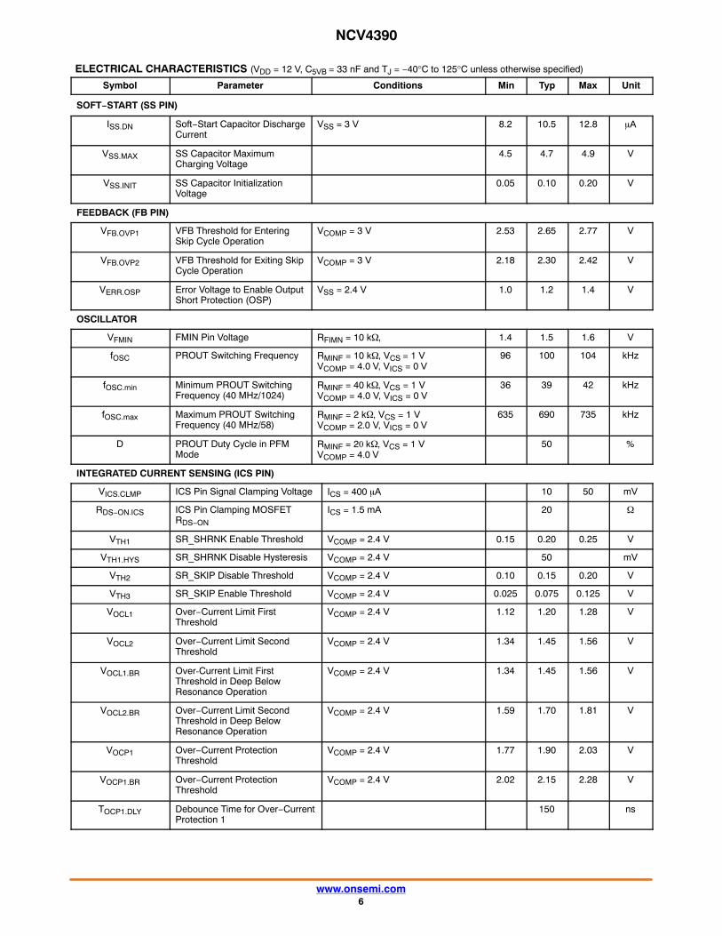
ELECTRICAL CHARACTERISTICS (VDD = 12 V, C5VB = 33 nF and TJ = −40°C to 125°C unless otherwise specified)
Symbol Parameter Conditions Min Typ Max Unit
SUPPLY VOLTAGE (VDD PIN)
ISTARTUP Startup Supply Current VDD = 9 V 80 115 �A
IDD Operating Current VCOMP = 0.1 V, VFB = 3 V, VSS = 0 V 2.8 mA
IDD_DYM1 Dynamic Operating Current fSW = 100 kHz; CL = 1 nF, with PR Operation Only
10 mA
IDD_DYM2 Dynamic Operating Current fSW = 100 kHz; CL = 1 nF, with PR &SR Operation
13 mA
VDD.ON VDD ON Voltage (VDD Rising) 9 10 11 V
VDD.OFF VDD OFF Voltage (VDD Falling)
8.6 V
VDD.HYS UVLO Hysteresis 0.9 1.4 1.9 V
REFERENCE VOLTAGE
V5VB 5 V Reference TJ = 25°C 4.99 5.05 5.11 V
−40°C < TJ < 125°C 4.90 5.05 5.20 V
ERROR AMPLIFIER (COMP PIN)
VSS.CLMP Voltage Feedback Reference TJ = 25°C 2.37 2.40 2.43 V
−40°C < TJ < 125°C 2.34 2.40 2.46 V
gm Error Amplifier Gain Transconductance
300 �mho
ICOMP1 Error Amplifier Maximum Output Current (Sourcing)
VFB = 1.8 V, VCOMP = 2.5 V 67 90 115 �A
ICOMP2 Error Amplifier Maximum Output Current (Sinking)
VFB = 3.0 V, VCOMP = 2.5 V 67 90 115 �A
VCOMP.CLMP1 Error Amplifier Output HighClamping Voltage
VFB = 1.8 V 4.2 4.4 4.6 V
VCOMP.PWM VCOMP Internal Clamping Voltage for PWM Operation
RPWM = 130 k 1.26 1.41 1.56 V
RPWM = 82 k 1.4 1.6 1.8 V
VPWMS PWMS Pin Voltage RPWM = 82 k 1.9 2.0 2.1 V
VCOMP.SKP VCOMP Threshold for EnteringSkip Cycle Operation
1.15 1.25 1.35 V
VCOMP.SKP.HYS VCOMP Threshold Hysteresisfor Entering Skip Cycle Operation
50 mV
DEAD TIME (DT PIN)
IDT Dead−Time Programming Current
VRDT = 1.2 V 140 150 160 �A
VTHDT1 First Threshold for Dead−TimeDetection
0.9 1.0 1.1 V
VTHDT2 Second Threshold for Dead−Time Detection
2.8 3.0 3.2 V
VRDT.ON VRDT ON Voltage (VRDT Rising)
1.2 1.4 1.6 V
SOFT−START (SS PIN)
ISS.T Total Soft−Start Current (Including ISS.UP)
VSS = 1 V 32 40 52 �A
VOLP Overload Protection Threshold 3.45 3.60 3.75 V
ISS.UP Soft−Start Capacitor ChargeCurrent for Delayed Shutdown
VSS = 3 V 8.2 10.5 12.8 �A
NCV4390
www.onsemi.com6
ELECTRICAL CHARACTERISTICS (VDD = 12 V, C5VB = 33 nF and TJ = −40°C to 125°C unless otherwise specified)
Symbol UnitMaxTypMinConditionsParameter
SOFT−START (SS PIN)
ISS.DN Soft−Start Capacitor DischargeCurrent
VSS = 3 V 8.2 10.5 12.8 �A
VSS.MAX SS Capacitor Maximum Charging Voltage
4.5 4.7 4.9 V
VSS.INIT SS Capacitor Initialization Voltage
0.05 0.10 0.20 V
FEEDBACK (FB PIN)
VFB.OVP1 VFB Threshold for EnteringSkip Cycle Operation
VCOMP = 3 V 2.53 2.65 2.77 V
VFB.OVP2 VFB Threshold for Exiting SkipCycle Operation
VCOMP = 3 V 2.18 2.30 2.42 V
VERR.OSP Error Voltage to Enable OutputShort Protection (OSP)
VSS = 2.4 V 1.0 1.2 1.4 V
OSCILLATOR
VFMIN FMIN Pin Voltage RFIMN = 10 k�, 1.4 1.5 1.6 V
fOSC PROUT Switching Frequency RMINF = 10 k�, VCS = 1 V VCOMP = 4.0 V, VICS = 0 V
96 100 104 kHz
fOSC.min Minimum PROUT SwitchingFrequency (40 MHz/1024)
RMINF = 40 k�, VCS = 1 V VCOMP = 4.0 V, VICS = 0 V
36 39 42 kHz
fOSC.max Maximum PROUT SwitchingFrequency (40 MHz/58)
RMINF = 2 k�, VCS = 1 V VCOMP = 2.0 V, VICS = 0 V
635 690 735 kHz
D PROUT Duty Cycle in PFMMode
RMINF = 20 k�, VCS = 1 V VCOMP = 4.0 V
50 %
INTEGRATED CURRENT SENSING (ICS PIN)
VICS.CLMP ICS Pin Signal Clamping Voltage ICS = 400 �A 10 50 mV
RDS−ON.ICS ICS Pin Clamping MOSFET RDS−ON
ICS = 1.5 mA 20 �
VTH1 SR_SHRNK Enable Threshold VCOMP = 2.4 V 0.15 0.20 0.25 V
VTH1.HYS SR_SHRNK Disable Hysteresis VCOMP = 2.4 V 50 mV
VTH2 SR_SKIP Disable Threshold VCOMP = 2.4 V 0.10 0.15 0.20 V
VTH3 SR_SKIP Enable Threshold VCOMP = 2.4 V 0.025 0.075 0.125 V
VOCL1 Over−Current Limit First Threshold
VCOMP = 2.4 V 1.12 1.20 1.28 V
VOCL2 Over−Current Limit SecondThreshold
VCOMP = 2.4 V 1.34 1.45 1.56 V
VOCL1.BR Over-Current Limit First Threshold in Deep Below Resonance Operation
VCOMP = 2.4 V 1.34 1.45 1.56 V
VOCL2.BR Over−Current Limit SecondThreshold in Deep Below Resonance Operation
VCOMP = 2.4 V 1.59 1.70 1.81 V
VOCP1 Over−Current Protection Threshold
VCOMP = 2.4 V 1.77 1.90 2.03 V
VOCP1.BR Over−Current Protection Threshold
VCOMP = 2.4 V 2.02 2.15 2.28 V
TOCP1.DLY Debounce Time for Over−CurrentProtection 1
150 ns

NCV4390
www.onsemi.com7
ELECTRICAL CHARACTERISTICS (VDD = 12 V, C5VB = 33 nF and TJ = −40°C to 125°C unless otherwise specified)
Symbol UnitMaxTypMinConditionsParameter
CURRENT SENSING (CS PIN)
VOCP2P Over−Current Protection Threshold
3.3 3.5 3.7 V
TOCP2.DLY Debounce Time for Over−CurrentProtection 2
150 ns
VOCP2N Over−Current Protection Threshold
−4.0 −3.5 −3.0 V
VCS.NZVS CS Signal Threshold for Non-ZVSDetection
VCOMP = 3.5 V 0.24 0.30 0.36 V
VCOMP.NZVS COMP Threshold for Non-ZVSDetection
VCS = 0.1 V 2.7 3.0 3.3 V
GATE DRIVE (PROUT1 AND PROUT2)
ISINK PROUT Sinking Current VPROUT1 & VPROUT2 = 6 V 140 mA
ISOURCE PROUT Sourcing Current VPROUT1 & VPROUT2 = 6 V 150 mA
tPR.RISE Rise Time VDD = 12 V, CL = 1 nF, 10% to 90% 100 ns
tPR.FALL Fall Time VDD = 12 V, CL = 1 nF, 90% to 10% 85 ns
SYNCHRONOUS RECTIFICATION (SR) CONTROL
TRC_SRCD (Note 1)
Internal RC Time Constant SRConduction Detection
50 100 150 ns
VSRCD.OFFSET1 (Note 1)
Internal Comparator Offset RisingEdge Detection
0.15 0.25 0.35 V
VSRCD.OFFSET2(Note 1)
Internal Comparator Offset Falling Edge Detection
0.10 0.20 0.30 V
VSRCD.LOW SR Conduction Detect threshold 0.4 0.5 0.6 V
TDLY.CMP.SR SR Conduction Detect Comparator Delay
65 ns
VFB.SR.ON SR Enable FB Voltage 1.6 1.8 2.0 V
VFB.SR.OFF SR Disable FB Voltage 1.0 1.2 1.4 V
SR OUTPUT (SROUT1 AND SROUT2)
ISR.SINK PROUT Sinking Current VSROUT1 & VSROUT2 = 6 V 140 mA
ISR.SOURCE PROUT Sourcing Current VSROUT1 & VSROUT2 = 6 V 150 mA
tSR.RISE Rise Time VDD = 12 V, CL = 1 nF, 10% to 90% 100 ns
tSR.FALL Fall Time VDD =12 V, CL = 1 nF, 90% to 10% 85 ns
Product parametric performance is indicated in the Electrical Characteristics for the listed test conditions, unless otherwise noted. Productperformance may not be indicated by the Electrical Characteristics if operated under different conditions.1. These parameters, although guaranteed by design, are not production tested.
NCV4390
www.onsemi.com8
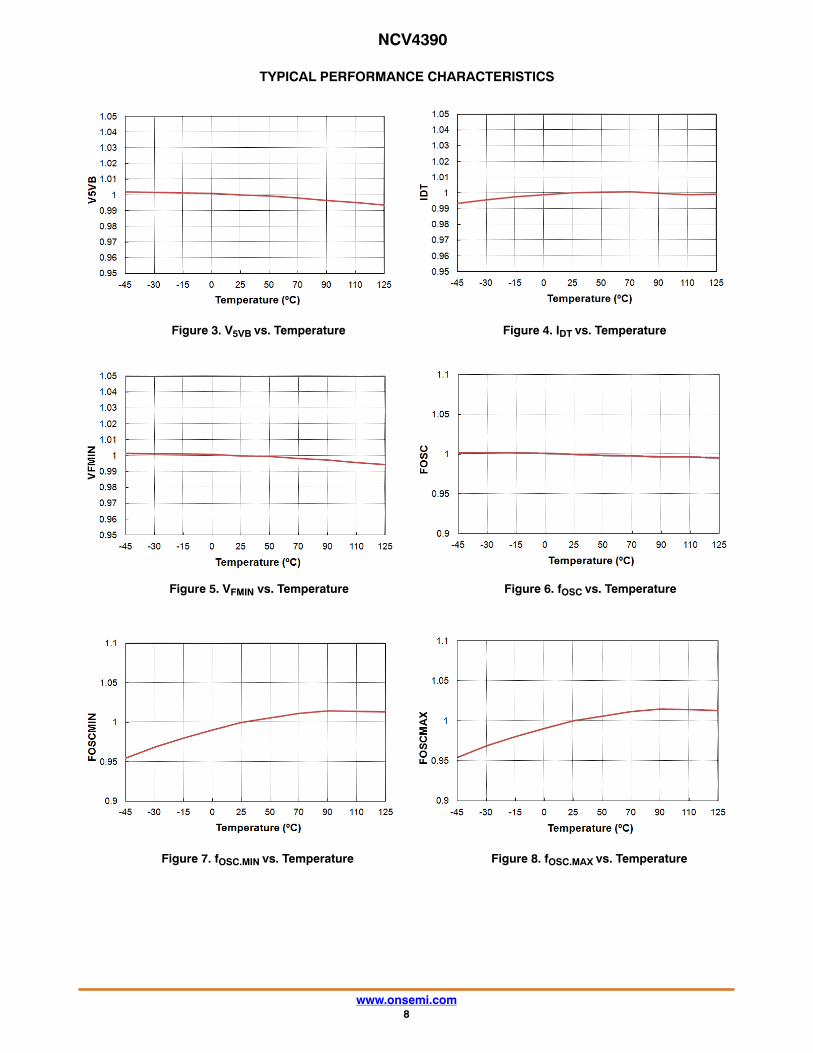
TYPICAL PERFORMANCE CHARACTERISTICS
Figure 3. V5VB vs. Temperature Figure 4. IDT vs. Temperature
Figure 5. VFMIN vs. Temperature Figure 6. fOSC vs. Temperature
Figure 7. fOSC.MIN vs. Temperature Figure 8. fOSC.MAX vs. Temperature

NCV4390
www.onsemi.com9
TYPICAL PERFORMANCE CHARACTERISTICS
Figure 9. DUTY CYCLE vs. Temperature Figure 10. VRDT.OFF vs. Temperature
Figure 11. VSS.CLMP vs. Temperature Figure 12. ISTARTUP vs. Temperature
Figure 13. IDD vs. Temperature Figure 14. IDD_DYM1 vs. Temperature

NCV4390
www.onsemi.com10
TYPICAL PERFORMANCE CHARACTERISTICS
Figure 15. IDD_DYM2 vs. Temperature Figure 16. VDD.ON vs. Temperature
Figure 17. VDD.OFF vs. Temperature Figure 18. VDD.HYS vs. Temperature
Figure 19. gm vs. Temperature Figure 20. ICOMP1 vs. Temperature

NCV4390
www.onsemi.com11
TYPICAL PERFORMANCE CHARACTERISTICS
Figure 21. ICOMP2 vs. Temperature Figure 22. VCOMP.CLMP1 vs. Temperature
Figure 23. VCOMP.PWM vs. Temperature Figure 24. VCOMP.SKIP vs. Temperature
Figure 25. VCOMP.SKIP.HYS vs. Temperature Figure 26. VRDT.ON vs. Temperature

NCV4390
www.onsemi.com12
TYPICAL PERFORMANCE CHARACTERISTICS
Figure 27. VTHDT1 vs. Temperature Figure 28. VTHDT2 vs. Temperature
Figure 29. ISS.T vs. Temperature Figure 30. VOLP vs. Temperature
Figure 31. ISS.UP vs. Temperature Figure 32. VSS.MAX vs. Temperature

NCV4390
www.onsemi.com13
TYPICAL PERFORMANCE CHARACTERISTICS
Figure 33. ISS.DN vs. Temperature Figure 34. VSS.INIT vs. Temperature
Figure 35. VPWMS vs. Temperature Figure 36. VFB.OVP1 vs. Temperature
Figure 37. VFB.OVP1 vs. Temperature Figure 38. VERR.OSP vs. Temperature

NCV4390
www.onsemi.com14
TYPICAL PERFORMANCE CHARACTERISTICS
Figure 39. RDS−ON.ICS vs. Temperature Figure 40. VTH1 vs. Temperature
Figure 41. VTH1 vs. Temperature Figure 42. VTH3 vs. Temperature
Figure 43. VOCL1 vs. Temperature Figure 44. VOCL2 vs. Temperature

NCV4390
www.onsemi.com15
TYPICAL PERFORMANCE CHARACTERISTICS
Figure 45. VOCL1.BR vs. Temperature Figure 46. VOCL2.BR vs. Temperature
Figure 47. VOCP1 vs. Temperature Figure 48. VOCP1.BR vs. Temperature
Figure 49. VOCP2P vs. Temperature Figure 50. VOCP2N vs. Temperature

NCV4390
www.onsemi.com16
TYPICAL PERFORMANCE CHARACTERISTICS
Figure 51. VCS.NZVS vs. Temperature Figure 52. VCOMP.NZVS vs. Temperature

NCV4390
www.onsemi.com17
APPLICATION INFORMATIONOperation Principle of Charge Current Control
The LLC resonant converter has been widely used formany applications because it can regulate the output overentire load variations with a relatively small variation ofswitching frequency, and achieve Zero Voltage Switching(ZVS) for the primary side switches and Zero CurrentSwitching (ZCS) for the secondary side rectifiers over theentire operating range. In addition, the resonant inductancecan be integrated with the transformer into a single magneticcomponent. Figure 53 shows the simplified schematic of theLLC resonant converter where voltage mode control isemployed. Voltage mode control is typically used for theLLC resonant converter where the error amplifier outputvoltage directly controls the switching frequency. However,the compensation network design of the LLC resonantconverter is relatively challenging since the frequencyresponse with voltage mode control includes four poleswhere the location of the poles changes with input voltageand load variations.
NCV4390 employs charge current mode control toimprove the dynamic response of the LLC resonantconverter. Figure 54 shows the simplified schematic of ahalf−bridge LLC resonant converter using NCV4390,where Lm is the magnetizing inductance, Lr is the resonantinductor and Cr is the resonant capacitor. Typical keywaveforms of the LLC resonant converter for heavy loadand light load conditions are illustrated in Figure 55 andFigure 56, respectively. It is assumed that the operationfrequency is same as the resonance frequency, as determinedby the resonance between Lr and Cr. Since the primary−sideswitch current does not increase monotonically, the switchcurrent itself cannot be used forpulse−frequency−modulation (PFM) for the output voltageregulation. Also, the peak value of the primary−side currentdoes not reflect the load condition properly because the largecirculating current (magnetizing current) is included in theprimary−side switch current. However, the integral of theswitch current (VICS) does increase monotonically and hasa peak value similar to that used for peak current modecontrol, as shown in Figure 55 and Figure 56.
Thus, NCV4390 employs charge current control, whichcompares the total charge of the switch current (integral ofswitch current) to the control voltage to modulate theswitching frequency. Since the charge of the switch currentis proportional to the average input current over oneswitching cycle, charge control provides a fast inner loopand offers excellent transient response including inherentline feed−forward. The PFM block has an internal timingcapacitor (CT) whose charging current is determined by the
current flowing out of the FMIN pin. The FMIN pin voltageis regulated at 1.5 V.
Figure 53. LLC Resonant Converter with VoltageMode Control
Q2
VINVO
COLrCr
Q1
+
−Driver
VO.REF
VCO
VC
Vc
L
Figure 54. Schematic of LLC resonant ConverterPower Stage Schematic
FMIN
+
−
+
−
1.5V
VREFReset
CT
Currentsensing
VCT
VSAW
Integrated signal (VICS)
U1
VO
Cr Lr
Lm
DigitalOSC
VIN Q1
Q2
PROUT1
PROUT2
VCOMP.I
VSAW
1V
VCOMP
1V
PROUT2
PROUT1
PROUT1
2.4V SS
FBCOMP
PROUT2
+
− 3V
VCOMP.I
PWMcontrol
PWMS
ICS
COMPCutback
3/4
There is an upper limit (3 V) for the timing capacitorvoltage, which determines the minimum switchingfrequency for a given resistor connected to the FMIN pin.The sawtooth waveform (VSAW) is generated by adding theintegral of the Q1 switch current (VICS) and the timing

NCV4390
www.onsemi.com18
capacitor voltage (VCT) of the oscillator. The sawtoothwaveform (Vsaw) is then compared with the compensationvoltage (VCOMP) to determine the switching frequency.
Figure 55. Typical Waveforms of the LLCResonant Converter for Heavy Load Condition
Ip
IDS1
Im
ID
VICS = k ∫ IDS1dt
Ip
IDS1
Im
ID
Figure 56. Typical Waveforms of LLC ResonantConverter for Light−Load Condition
VICS = k ∫ IDS1dt
Hybrid Control (PWM + PFM)The conventional PFM control method modulates only
the switching frequency with a fixed duty cycle of 50%,which typically results in relatively poor light loadefficiency due to the large circulating primary side current.
To improve the light load efficiency, NCV4390 employshybrid control where the PFM is switched to pulse widthmodulation (PWM) mode at light load as illustrated inFigure 57. If want to not uses PWM mode in light loadcondition, adjust PWM entry level using external PWMresistor for under skip threshold level. The figure 58 showthat the switching frequency and duty ratio characteristics indisable PWM mode. The typical waveforms for PFM modeand PWM mode are shown in Figure 59 and Figure 60,respectively. When the error amplifier voltage (VCOMP) isbelow the PWM mode threshold, the internal COMP signalis clamped at the threshold level and the PFM operationswitches to PWM mode.
Figure 57. Mode Change with COMP Voltage
Switchingfrequency
VCOMP
4.4VVCOMP.PWM
Duty cycle
D=50%
1.25V
PFM ModePWM ModeSkip cycle
Noswitching
1.3V
Figure 58. Disable PWM mode with COMP Voltage
Switchingfrequency
VCOMP
4.4V
VCOMP.PWM = Less than 1.25 V( Disable PWM mode )
Duty cycle
D=50%
1.25V
PFM ModeSkip cycle
Noswitching
1.3V
Figure 59. Key Waveforms of PFM Operation
PROUT1 PROUT2
IpIm
VICS
VCT
*VICS+VCT
VCOMP
Counter of
3/4

NCV4390
www.onsemi.com19
Figure 60. Key Waveforms of PWM Operation
PROUT1 PROUT2
VICS
VCT
*VICS+VCT
VCOMP
Counter ofdigital OSC
VTH.PWM
Ip
VCOMP.PWM −VCOMP
VCOMP.PWM −VCOMP
3/4
In PWM mode, the switching frequency is fixed by theclamped internal COMP voltage (VCOMPI) and the dutycycle is determined by the difference between COMPvoltage and the PWM mode threshold voltage. Thus, theduty cycle decreases as VCOMP drops below the PWMmode threshold, which limits the switching frequency atlight load condition as illustrated in Figure 57. The PWMmode threshold can be programmed between 1.9 V andunder skip threshold using a resistor on the PWMS pin.Disable PWM mode when the PWM mode threshold is setbelow 1.25 V.
Current SensingNCV4390 senses instantaneous switch current and the
integral of the switch current as illustrated in Figure 61.Since NCV4390 is located in the secondary side, it is typicalto use a current transformer for sensing the primary sidecurrent. While the PROUT1 is LOW, the ICS pin is clampedat 0 V with an internal reset MOSFET. Conversely, whilePROUT1 is high, the ICS pin is not clamped and the integralcapacitor (CICS) is charged and discharged by the voltagedifference between the sensing resistor voltage (VSENSE)and the ICS pin voltage. During normal operation, thevoltage of the ICS pin is below 1.2 V since the power limitthreshold is 1.2 V. The current sensing resistor and currenttransformer turns ratio should be designed such that thevoltage across the current sensing resistor (VSENSE) isgreater than 4 V at the full load condition. Therefore thecurrent charging and discharging CICS should be almostproportional to the voltage across the current sensingresistor (VSENSE). Figure 62 compares the VICS signal andthe ideal integral signal when the amplitude of VSENSE is4 V. As can be seen, there is about 10% error in the VICSsignal compared to the ideal integral signal, which isacceptable for most designs. If more accuracy of the VICSis required, the amplitude of VSENSE should be increased.
Figure 61. Current Sensing of NCV4390
+
−
PROUT1
PROUT1
VSENSE
PROUT1
VICS
Primarywinding
VICS
+
−
VCTX VICS
ICS
CICS
RICS
CSVCS
Q1
Q2
Currenttransformer
Maintransformer
PROUT1
PROUT2
RCS2
RCS1
Figure 62. Disable PWM mode with COMP Voltage
0
0.2
0.4
0.6
0.8
1
−4
−3
−2
−1
0
1
2
3
VICS
VCTX
4
∫ VCTXdt
Since the peak value of the integral of the current sensingvoltage (VICS) is proportional to the average input currentof the LLC resonant converter, it is used for four mainfunctions, listed and shown in Figure 63.
1. SR Gate Shrink: To guarantee stable SR operationduring light load operation, the SR dead time (bothof turn−on and turn−off transitions) is increasedresulting in SR gate shrink when VICS peak valuedrops below VTH1 (0.2 V). The SR dead time isreduced to the programmed value when VICS peakvalue rises above 0.25 V
2. SR Disable and Enable: During very light−loadcondition, the SR is disabled when the VICS peakvalue is smaller than VTH3 (0.075 V). When theVICS peak value increases above VTH2 (0.15 V),the SR is enabled

NCV4390
www.onsemi.com20
3. Over−Current Limit: The VICS peak value is alsoused for input current limit. As can be seen inFigure 64, there exist two different current limits(fast and slow). When the VICS peak valueincreases above the slow current limit level(VOCL1) due to a mild overload condition, theinternal feedback compensation voltage is slowlyreduced to limit the input power. This continuesuntil the VICS peak value drops below VOCL1.During a more severe over load condition, theVICS peak value crosses the fast current limitthreshold (VOCL2) and the internal feedbackcompensation voltage is quickly reduced to limitthe input power as shown in Figure 64 (b). Thiscontinues until the VICS peak value drops belowVOCL2. The current limit threshold on the VICSpeak value also changes as the output voltagesensing signal (VFB) decreases such that outputcurrent is limited during overload condition asshown in Figure65. In addition, these limitthresholds change to higher values (VOCL1.BR andVOCL2.BR) when the converter operates in deepbelow resonance operation for a longer holduptime (refer to holdup time boost function)
4. Over−Current Protection (OCP1): When the VICSpeak value is larger than VOCP1 (1.9 V), the overcurrent protection is triggered. 150 ns debouncetime is added for over−current protection. TheseOCP threshold can be changed to a higher value(VOCP1.BR) when the converter operates in deepbelow resonance operation for a longer holduptime (refer to holdup time boost function)
Figure 63. Functions Related to VICS Peak Voltage
1.2V
Output Power
SR Disable
SR Enable
Fast Current limit
Slow Current limit
SR Shrink
1.45V0.2V0.15V0.075V
50mV
VICS
VICSPK
Figure 64. Current Limit of the ICS Pin byFrequency Shift (Compensation Cutback)
PROUT1
IPR
VOCL1
VOCL2
V
PROUT1
IPR
VOCL1
VOCL2
V
(a) Mild Overload Condition
(b) Severe Overload Condition
OCP1
OCP1
Figure 65. Current Limit Threshold Modulation asa Function of Feedback Voltage
VFB
VOCL1
0.5V
1.45V
2.4 V
VOCL2
0.75V
1.0V
1.2V
2.0 V

NCV4390
www.onsemi.com21
The instantaneous switch current sensing on the CS pin isalso used for the following functions.
1. Non−ZVS Prevention: When the compensationvoltage (VCOMP) is higher than 3 V and VCS peakvalue is smaller than 0.3 V at PROUT1 fallingedge, non−ZVS condition is detected, whichdecreases the internal compensation signal toincrease the switching frequency
2. Over−Current Protection (OCP2): When VCS ishigher than 3.5 V or lower than −3.5 V,over−current protection (OCP2) is triggered. Theinstantaneous primary side current is also sensedon CS pin. Since the OCP2 thresholds on the CSpin are 3.5 V and −3.5 V as shown in Figure 66,the CS signal is typically obtained from VSENSEby using a voltage divider as illustrated inFigure 61. 150 ns debounce time is also added forOCP2
Figure 67 shows utilization of current sensing by usingICS and CS signals.
Figure 66. Over−Current Protection of the CS Pin
PROUT1
VCS
PROUT2
PROUT1
VCS
PROUT2
(3.5)V
(−3.5V)
VOCP2P
VOCP2N
(3.5)VVOCP2P
(−3.5V)VOCP2N
Figure 67. Utilization of Current Sensing Signal
+
−1.9V
+
−3.5V
+
−
− 3.5V
CS
ICS
OCP
OCP1
OCP2
+
−
0.3V
PROUT1
D Q
QN
+
−
0.25V /0.20V
PROUT1
D Q
QN
SR Shrink
+
−
0.15V /0.075V
PROUT1
D Q
QN
SR Skip
+
−OCL1
PROUT1
D Q
QN
+
−OCL2
PROUT1
D Q
QN
CompensationCutback
NON ZVS detect
+
−
COMP
3V
CompensationVoltage
CompensationCutback
PFM block

NCV4390
www.onsemi.com22
Soft−Start and Output Voltage RegulationFigure 68 shows the simplified circuit block for feedback
control and closed loop soft−start. During normal, steadystate operation, the Soft−Start (SS) pin is connected to thenon−inverting input of the error amplifier which is clampedat 2.4 V. The feedback loop operates such that the sensedoutput voltage is same as the SS pin voltage. During startup,an internal current source (ISS.T) charges the SS capacitorand SS pin voltage progressively increases. Therefore, theoutput voltage also rises monotonically as a result of closedloop SS control.
The SS capacitor is also used for the shutdown delay timeduring overload protection (OLP). Figure 69 shows the OLPwaveform. During normal operation, the SS capacitorvoltage is clamped at 2.4 V. When the output is over−loaded,VCOMP is saturated to HIGH and the SS capacitor isdecoupled from the clamping circuit through the SS controlblock. ISS is blocked by DBLCK and the SS capacitor isslowly charged up by the current source ISS.UP. When the SScapacitor voltage reaches 3.6 V, OLP is triggered. The timerequired for the soft−start capacitor to be charged from 2.4 Vto 3.6 V determines the shutdown delay time for overloadprotection.
Figure 68. Schematic of Closed Loop Soft−Start
SSControl
COMP FB
SS
ISS.UP
ISS.DN
ISS
Disable SSclamp
UP
DN
VO
Cr Lr
Lm
VIN Q1
Q2
PROUT1 PROUT2
PFM
2.4V
DBLCK
30 �A 10 �A
10 �A
Figure 69. Delayed Shutdown with Soft−Start
VSS
2.4V
3.6V
4.8V
Ip
time
time
Auto−Restart after ProtectionAll protections of NCV4390 are non−latching,
auto−restart, where the delayed restart is implemented bycharging and discharging the SS capacitor as illustrated inFigure 70. During normal operation, the SS capacitorvoltage is clamped at 2.4 V. Once any protection is triggered,the SS clamping circuit is disabled. The SS capacitor is thencharged up to 4.7 V by an internal current source (ISS.UP).The SS capacitor is then discharged down to 0.1 V byanother internal current (ISS.DN). After charging anddischarging the SS capacitor three more times, auto recoveryis enabled.
Figure 70. Auto Re−Start after Protection isTriggered
VSS
2.4V
3.6V
4.7V
Shutdowndelay
Discharged by I SS.DNCharged by ISS.UP
Ip
ICS
1.2V
VCOMP
1/8 time scale
0.1V
Charged by ISS.T
time
time
time
time

NCV4390
www.onsemi.com23
Output Short ProtectionTo minimize the power dissipation through the power
stage during a severe fault condition, NCV4390 offersOutput Short Protection (OSP). When the output is heavilyover−loaded or short circuited, the feedback voltage (outputvoltage sensing) does not follow the reference voltage of theerror amplifier (2.4 V). When the difference between thereference voltage of the error amplifier and the FB voltageis larger than 1.2 V, the OSP is triggered without waitinguntil the OLP is triggered as shown in Figure 71.
Dead−Time SettingWith a single pin (RDT pin), the dead times between the
primary side gate drive signals (PROUT1 and PROUT2)and secondary side SR gate drive signal (SROUT1 andSROUT2) are programmed using a switched current sourceas shown in Figure 72 and Figure 73. Once the 5 V bias isenabled, the RDT pin voltage is pulled up. When the RDTpin voltage reaches 1.4 V, the voltage across CDT is thendischarged down to 1 V by an internal current source IDT.IDT is then disabled and the RDT pin voltage is charged upby the RDT resistor. As shown in Figure 73, 1/64 of the timerequired (TSET1) for RDT pin voltage to rise from 1 V to 3 Vdetermines the dead time between the secondary side SRgate drive signals.
The switched current source IDT is then enabled and theRDT pin voltage is discharged. 1/32 of the time required(TSET2) for the RDT pin voltage to drop from 3 V to 1 Vdetermines the dead time between the primary side gatedrive signals. After the RDT voltage drops to 1 V, the currentsource IDT is disabled a second time, allowing the RDTvoltage to be charged up to 5 V.
Table 1 shows the dead times for SROUT and PROUTprogrammed with recommended RDT and CDT componentvalues. Since the time is measured by an internal 40 MHzclock signal, the resolution of the dead time setting is 25 ns.
Figure 71. Output Short Protection
VSS
2.4V
3.6V
4.8V
Ip
VICS
1.2V
0.0V
VFB
1.2V
time
time
Figure 72. Internal Current Source for of RDT Pin
5VB
VRDT
S1
IDT
RDT
CDT
Figure 73. Multi−function Operation of RDT Pin
1V
2V
3V
4V
5V
TSET1 TSET2
TSET1 / 64= SROUT Dead TimeTSET2 / 32 =PROUT Dead Time
The minimum and maximum dead times are thereforelimited at 75 ns and 375 ns respectively. To assure stable SRoperation while taking circuit parameter tolerance intoaccount, 75 ns dead time is not recommended especially forthe SR dead time.
When NCV4390 operates in PWM mode at light−loadcondition, the dead time is doubled to reduce the switchingloss.

NCV4390
www.onsemi.com24
Table 1. DEAD TIME SETTING FOR PROUT AND SROUT
CDT = 180 pF CDT = 220 pF CDT = 270pF CDT = 330 pF CDT = 390 pF CDT = 470 pF CDT = 560 pF
RDTSROUTDT (ns)
PROUTDT (ns)
SROUTDT (ns)
PROUTDT (ns)
SROUTDT (ns)
PROUTDT (ns)
SROUTDT (ns)
PROUTDT (ns)
SROUTDT (ns)
PROUTDT (ns)
SROUTDT (ns)
PROUTDT (ns)
SROUTDT (ns)
PROUTDT (ns)
28 k 75 375 75 375 75 375 100 375 125 375 150 375 175 375
30 k 75 250 75 325 100 375 100 375 125 375 150 375 175 375
33 k 75 200 75 250 100 300 125 375 150 375 175 375 200 375
36 k 75 175 75 200 100 250 125 325 150 375 175 375 225 375
40 k 75 150 100 175 125 225 150 275 175 325 200 375 250 375
44 k 75 125 100 150 125 200 150 250 175 300 225 350 275 375
48 k 100 125 125 150 150 175 175 225 200 275 250 325 300 375
53 k 100 100 125 125 150 175 200 200 225 250 275 300 325 375
58 k 125 100 150 125 175 150 200 200 250 250 300 300 350 350
64 k 125 100 150 125 175 150 225 200 275 225 325 275 375 325
71 k 150 100 175 125 200 150 250 175 300 225 350 250 375 325
78 k 150 100 175 100 225 150 275 175 325 200 375 250 375 300
86 k 175 75 200 100 250 125 300 175 375 200 375 250 375 300
94 k 175 75 225 100 275 125 325 175 375 200 375 225 375 275
104 k 200 75 250 100 300 125 375 150 375 200 375 225 375 275
114 k 225 75 275 100 325 125 375 150 375 175 375 225 375 275
126 k 250 75 300 100 375 125 375 150 375 175 375 225 375 275
138 k 275 75 325 100 375 125 375 150 375 175 375 225 375 250
152 k 300 75 350 100 375 125 375 150 375 175 375 225 375 250
Minimum Frequency SettingThe minimum switching frequency is limited by
comparing the timing capacitor voltage (VCT) with aninternal 3 V reference as shown in Figure 74. Since the risingslope of the timing capacitor voltage is determined by theresistor (RFMIN) connected to FMIN pin, the minimumswitching frequency is given as:
fSW .MIN � 100 kHz �
10 k�RFMIN
(eq. 1)
The minimum programmable switching frequency islimited by the digital counter running on an internal 40 MHzclock. Since a 10 bit counter is used, the minimum switchingfrequency given by the digital oscillator is 39 kHz
(40 MHz/1024 = 39 kHz). Therefore, the maximumallowable value for RFMIN is 25.5 K�.
PWM Mode Entry Level SettingWhen the COMP voltage drops below VCOMP.PWM as a
result of decreasing load, the internal COMP signal isclamped at the threshold level and PFM operation switchesto PWM Mode. The PWM entry level threshold isprogrammed using a external resistor on the PWMS pin asshown in Figure 75. Once NCV4390 enters into PWMmode, the SR gate drives are disabled. If want to usesspecially disable PWM mode, open PWMS pin or connectto 1 M�.

NCV4390
www.onsemi.com25
Skip Cycle OperationAs illustrated in Figure 76, when the COMP voltage drops
below VCOMP.SKIP (1.25 V) as a result of decreasing load,skip cycle operation is employed to reduce switching losses.As the COMP voltage rises above 1.3 V, the switchingoperation is resumed. When the FB voltage rises aboveVFB.OVP1 (2.65 V), the skip cycle operation is also enabledto limit the output voltage rising quickly. As the FB voltagedrops below VFB.OVP2 (2.3 V), the switching operation isresumed.
Figure 74. Minimum Switching Frequency Setting
FMIN
+
−
+
−
1.5V
VREFReset
CT
VCT
VSAW
Integrated signal (VICS)
U1
DigitalOSC
VCOMP.I
VSAW
1V
VCOMP
1V
PROUT2
PROUT1
PROUT1
2.4V SS
FBCOMP
PROUT2
+
− 3V
VCOMP.I
PWMcontrol
PWMS
ICS
COMPCutback
VSAW
PROUT2
PROUT1
VCOMP
1V
3V
1V
PROUT1
PROUT2
PROUT1
3V
1V
PROUT1
VCT VCT
(a) PFM by COM voltage
VCOMP
(b) minimum Frequency limit
Min Freq ComparatorRFMIN
+
−
Figure 75. PWM Mode Entry Level Setting
Figure 76. Skip Cycle Operation
Ip
VCOMP
VCOMP.SKIP
50mV
NCV4390 uses a dual edge tracking adaptive gate drivemethod that anticipates the SR current zero crossing instantwith respect to two different time references. Figure 77 andFigure 78 show the operational waveforms of the dual edgetracking adaptive SR drive method operating below andabove resonance. To simplify the explanation, the SR deadtime is assumed to be zero. The first tracking circuitmeasures SR conduction time (TSR_CNDCTN) and usesthis information to generate the first adaptive drive signal(VPRD_DRV1) for the next switching cycle whose durationis the same as the SR conduction time of previous switchingcycle. The second tracking circuit measures the turn−offextension time which is defined as time duration from thefalling edge of the primary side drive to the correspondingSR turn−off instant (TEXT). This information is then usedto generate the second adaptive drive signal (VPRD_DRV2)for the next switching cycle. When the turn−off of theprimary side drive signal is after the turn−off of thecorresponding SR for below resonance operation, thesecond adaptive SR drive signal is the same as thecorresponding primary side gate drive signal. However,when the turn−off of the primary side drive signal is beforethe turn−off instant of the corresponding SR for aboveresonance operation, the second adaptive SR drive signal isgenerated by extending the corresponding primary side gatedrive signal by TEXT of the previous switching cycle.
Since the turn off instant of the second adaptive gate drivesignal is extended by TEXT with respect to the falling edgeof the primary side gate drive signal, the duration of thissignal consequentially changes with switching frequency.By combining these two signals VPRD_DRV1 andVPRD_DRV2 with an AND gate, the optimal adaptive gatedrive signal is obtained.
The SR conduction times for SR1 and SR2 for eachswitching cycle are measured using a single pin (SR1DSpin). The SR1DS voltage and its delayed signal, resulting

NCV4390
www.onsemi.com26
from a 100 ns RC time constant, are compared as shown inFigure 79. When the SR is conducting, the SR1DS voltageis clamped to either ground or the high voltage rail (2 timesthe output voltage) as illustrated in Figure 80. Whereas,SR1DS voltage changes fast when there is a switchingtransition. When both of the SR MOSFETs are turned off,the SR1DS voltage oscillates. When the SR1DS voltagechanges faster than 0.25 V/100 ns on the rising edge and0.2 V/100 ns on the falling edge the switching transition ofthe SR conduction state is detected. Based on the detectedswitching transition, NCV4390 predicts the SR currentzero−crossing instant for the next switching cycle. The100 ns detection delay caused by the RC time constant iscompensated in the internal timing detection circuit for acorrect gate drive for SR.
Figure 77. Operation of Dual Edge TrackingAdaptive SR Control (below Resonance)
IDS.PRI
ISR
VPROUT VPROUT
IDS.PRI
ISR
TSR_CNDCTN (n)
VPRD1(n+1)VPRD1(n)
TSR_CNDCTN(n+1)
TSR_CNDCTN* (n)
VPRD2 (n+1)VPRD2 (n)
TEXT(n) TEXT(n+1)
TEXT* (n)
TSR_CNDCTN* (n−1)
Figure 78. Operation of Dual Edge TrackingAdaptive SR Control (above Resonance)
ISRISR
TSR_CNDCTN(n) TSR_CNDCTN(n+1)
TSR_CNDCTN* (n−1)
TEXT* (n)
TEXT(n) TEXT(n+1)
TSR_CNDCTN* (n)
IDS.PRI IDS.PRI
VPROUT
VPRD1 (n)
VPRD2 (n)
VPROUT
VPRD1 (n+1)
VPRD2
Figure 79. SR Conduction Detection with SinglePin (SR1DS Pin)
SR1
SR2
SR1DS
ISR1
ISR2
+
−
S
R
Q
Q
+
−
0.2V
0.25V
RC=100ns
+
−
0.5V
SR1_OFF
SR2_OFF
VSR1DS VRC
100ns
V
100ns
VSR1DSVRC
SR1_OFF becomes HIGHif V>0.25V
0.5V
SR2_OFF becomes HIGHif V>0.2V
SR1_OFF
SR2_OFF SR2_OFF
RDS2
RDS1
C
�
�
DS
if �
�V
Figure 80 and Figure 81 show the typical waveforms ofSR1DS pin voltage together with other key waveforms.Since the voltage rating of SR1DS pin is 5 V, the voltagedivider should be properly designed such that noover−voltage is applied to this pin. Additional bypasscapacitor (CDS) can be connected to SR1DS pin to improvenoise immunity. However, the equivalent time constantgenerated from the bypass capacitor and voltage dividerresistors should be smaller than the internal RC timeconstant (100 ns) of the detection circuit for proper SRcurrent zero crossing detection.
Figure 80. SR Conduction Detection Waveform atbelow Resonance Operation
VSR1.DS
Ip
ISR1
1V
2V
3V
4V
5V
ISR2

NCV4390
www.onsemi.com27
Figure 81. SR Conduction Detection Waveform atabove Resonance Operation
VSR1DS
Ip
ISR1
1V
2V
3V
4V
5V
I
Holdup Time Boost FunctionThe holdup time of an off−line supply is defined as the
time required for the output voltage to remain withinregulation after the AC input voltage is removed. Since theinput bulk capacitor voltage drops during the holdup time,more current is taken from the bulk capacitor to deliver thesame power to the load. With a fixed power limit level ofpower supply designed for nominal input voltage, theholdup time tends to be limited due to the increased inputcurrent of the power supply.
NCV4390 has a holdup time boost function whichincreases the current limit threshold on the ICS pin voltagewhen the LLC resonant converter operates in deep below
resonance operation during the holdup time as shown inFigure 82. This holdup time boost operation is enabled whenthe SR conduction time is smaller than 94% of the halfswitching cycle for longer than 1.6 ms. The current limitlevel on ICS pin is recovered to normal value when the SRconduction time is larger than 98% of the half switchingcycle for longer than 3.2 ms.
Figure 82. Holdup Time Boost Function Operation
1.2V
1.45V
VOCL1
Ipr
SR c onduc tion time
Half switc hing period
Half switc hing period
SR c onduc tion time< 94%
VOCL2
1.7V

NCV4390
www.onsemi.com28
QUICK SETUP GUIDELINE for CURRENT SENSING and SOFT−START
Assuming the switching frequency is the same as theresonance frequency, the peak voltage of the secondary sidevoltage of current transformer (VSENSE) is given as:
VSENSEPK
� IO ��2�
NS
NP�
1nCT
� (RCS1 � RCS2)
[example] IO = 20 A, NP = 35, NS = 2, nCT = 50,RCS1 + RCS2 = 100 � � VSENSE
PK = 3.59 V in nominalload condition.
The voltage divider on the CS pin should be selected suchthat OCP is not triggered during normal operation.
VCSPK
� IO ��2�
NS
NP�
1nCT
� RCS1 � 3.5 V
[example] IO = 21 A, NP = 35, NS = 2, nCT = 50,RCS1 = 30 �, RCS2 = 70 � � VCS
PK = 1.131 V in nominalload condition.
The resistor and capacitor on the ICS pin should beselected such that the current limit is not triggered duringnormal operation.
VICSPK
� IO �
NSNP
�1
nCT�
RCS1 � RCS2RICS
�1
CICS�
12
fSW � 1.2 V
[example] Io = 20 A, NP = 35, NS = 2, nCT = 50,RCS1 = 30 �, RCS2 = 70 �, RICS = 10 k�, CICS = 1 nF,fS = 100 kHz.� VICS
PK = 1.14 V in nominal load condition (actualVICS
PK is lower by about 10% as shown in Figure 62 due toa quasi integral effect).
Assuming the actual VICSPK (VICS
PKA) is 1 V, thesoft−start capacitor should be selected such that the overloadprotection is not triggered during startup with full loadcondition.
TSS �
CSS � 2.4 V
ISS� 40.8 ms �
COUT � VO
1.2�VICSPK
VICSPK � IO
� 22.5 ms
Figure 83. Basic Application Circuit for Current Sensing and Soft−Start
+
−
PROUT1
VSENSE
PROUT1
Primaryside
winding
VICS
+
−
VSENSE VICS
ICS
CICS
RICS
CS VCS
Q1
Q2
Currenttransformer
Maintransformer
PROUT1
PROUT2
FMIN
+
−
+
−
1.5V
VREF
CT
VCT
VSAW
Integrated signal (VICS)
U1
DigitalOSC
VCOMP.I
OCP
VCOMP
1V
PROUT1
2.4V SS
FBCOMP
PROUT2
+
− 3V
VCOMP.I
PWMcontrol
PWMS
COMPCutback
RFMIN
+
−
+
−
3.5V
−3.5V
ICSanalyzer
RCS2
RCS1
Secondary Side winding
NP
NS
NS
VO
COUT
1:nCT

SOIC−16CASE 751B−05
ISSUE KDATE 29 DEC 2006SCALE 1:1
NOTES:1. DIMENSIONING AND TOLERANCING PER ANSI
Y14.5M, 1982.2. CONTROLLING DIMENSION: MILLIMETER.3. DIMENSIONS A AND B DO NOT INCLUDE MOLD
PROTRUSION.4. MAXIMUM MOLD PROTRUSION 0.15 (0.006) PER SIDE.5. DIMENSION D DOES NOT INCLUDE DAMBAR
PROTRUSION. ALLOWABLE DAMBAR PROTRUSIONSHALL BE 0.127 (0.005) TOTAL IN EXCESS OF THE DDIMENSION AT MAXIMUM MATERIAL CONDITION.
1 8
16 9
SEATINGPLANE
F
JM
R X 45�
G
8 PLP−B−
−A−
M0.25 (0.010) B S
−T−
D
K
C
16 PL
SBM0.25 (0.010) A ST
DIM MIN MAX MIN MAXINCHESMILLIMETERS
A 9.80 10.00 0.386 0.393B 3.80 4.00 0.150 0.157C 1.35 1.75 0.054 0.068D 0.35 0.49 0.014 0.019F 0.40 1.25 0.016 0.049G 1.27 BSC 0.050 BSCJ 0.19 0.25 0.008 0.009K 0.10 0.25 0.004 0.009M 0 7 0 7 P 5.80 6.20 0.229 0.244R 0.25 0.50 0.010 0.019
� � � �
6.40
16X0.58
16X 1.12
1.27
DIMENSIONS: MILLIMETERS
1
PITCH
SOLDERING FOOTPRINT
STYLE 1:PIN 1. COLLECTOR
2. BASE3. EMITTER4. NO CONNECTION5. EMITTER6. BASE7. COLLECTOR8. COLLECTOR9. BASE
10. EMITTER11. NO CONNECTION12. EMITTER13. BASE14. COLLECTOR15. EMITTER16. COLLECTOR
STYLE 2:PIN 1. CATHODE
2. ANODE3. NO CONNECTION4. CATHODE5. CATHODE6. NO CONNECTION7. ANODE8. CATHODE9. CATHODE
10. ANODE11. NO CONNECTION12. CATHODE13. CATHODE14. NO CONNECTION15. ANODE16. CATHODE
STYLE 3:PIN 1. COLLECTOR, DYE #1
2. BASE, #13. EMITTER, #14. COLLECTOR, #15. COLLECTOR, #26. BASE, #27. EMITTER, #28. COLLECTOR, #29. COLLECTOR, #3
10. BASE, #311. EMITTER, #312. COLLECTOR, #313. COLLECTOR, #414. BASE, #415. EMITTER, #416. COLLECTOR, #4
STYLE 4:PIN 1. COLLECTOR, DYE #1
2. COLLECTOR, #13. COLLECTOR, #24. COLLECTOR, #25. COLLECTOR, #36. COLLECTOR, #37. COLLECTOR, #48. COLLECTOR, #49. BASE, #4
10. EMITTER, #411. BASE, #312. EMITTER, #313. BASE, #214. EMITTER, #215. BASE, #116. EMITTER, #1
STYLE 5:PIN 1. DRAIN, DYE #1
2. DRAIN, #13. DRAIN, #24. DRAIN, #25. DRAIN, #36. DRAIN, #37. DRAIN, #48. DRAIN, #49. GATE, #4
10. SOURCE, #411. GATE, #312. SOURCE, #313. GATE, #214. SOURCE, #215. GATE, #116. SOURCE, #1
STYLE 6:PIN 1. CATHODE
2. CATHODE3. CATHODE4. CATHODE5. CATHODE6. CATHODE7. CATHODE8. CATHODE9. ANODE
10. ANODE11. ANODE12. ANODE13. ANODE14. ANODE15. ANODE16. ANODE
STYLE 7:PIN 1. SOURCE N‐CH
2. COMMON DRAIN (OUTPUT)3. COMMON DRAIN (OUTPUT)4. GATE P‐CH5. COMMON DRAIN (OUTPUT)6. COMMON DRAIN (OUTPUT)7. COMMON DRAIN (OUTPUT)8. SOURCE P‐CH9. SOURCE P‐CH
10. COMMON DRAIN (OUTPUT)11. COMMON DRAIN (OUTPUT)12. COMMON DRAIN (OUTPUT)13. GATE N‐CH14. COMMON DRAIN (OUTPUT)15. COMMON DRAIN (OUTPUT)16. SOURCE N‐CH
16
8 9
8X
MECHANICAL CASE OUTLINE
PACKAGE DIMENSIONS
ON Semiconductor and are trademarks of Semiconductor Components Industries, LLC dba ON Semiconductor or its subsidiaries in the United States and/or other countries.ON Semiconductor reserves the right to make changes without further notice to any products herein. ON Semiconductor makes no warranty, representation or guarantee regardingthe suitability of its products for any particular purpose, nor does ON Semiconductor assume any liability arising out of the application or use of any product or circuit, and specificallydisclaims any and all liability, including without limitation special, consequential or incidental damages. ON Semiconductor does not convey any license under its patent rights nor therights of others.
98ASB42566BDOCUMENT NUMBER:
DESCRIPTION:
Electronic versions are uncontrolled except when accessed directly from the Document Repository.Printed versions are uncontrolled except when stamped “CONTROLLED COPY” in red.
PAGE 1 OF 1SOIC−16
© Semiconductor Components Industries, LLC, 2019 www.onsemi.com
onsemi, , and other names, marks, and brands are registered and/or common law trademarks of Semiconductor Components Industries, LLC dba “onsemi” or its affiliatesand/or subsidiaries in the United States and/or other countries. onsemi owns the rights to a number of patents, trademarks, copyrights, trade secrets, and other intellectual property.A listing of onsemi’s product/patent coverage may be accessed at www.onsemi.com/site/pdf/Patent−Marking.pdf. onsemi reserves the right to make changes at any time to anyproducts or information herein, without notice. The information herein is provided “as−is” and onsemi makes no warranty, representation or guarantee regarding the accuracy of theinformation, product features, availability, functionality, or suitability of its products for any particular purpose, nor does onsemi assume any liability arising out of the application or useof any product or circuit, and specifically disclaims any and all liability, including without limitation special, consequential or incidental damages. Buyer is responsible for its productsand applications using onsemi products, including compliance with all laws, regulations and safety requirements or standards, regardless of any support or applications informationprovided by onsemi. “Typical” parameters which may be provided in onsemi data sheets and/or specifications can and do vary in different applications and actual performance mayvary over time. All operating parameters, including “Typicals” must be validated for each customer application by customer’s technical experts. onsemi does not convey any licenseunder any of its intellectual property rights nor the rights of others. onsemi products are not designed, intended, or authorized for use as a critical component in life support systemsor any FDA Class 3 medical devices or medical devices with a same or similar classification in a foreign jurisdiction or any devices intended for implantation in the human body. ShouldBuyer purchase or use onsemi products for any such unintended or unauthorized application, Buyer shall indemnify and hold onsemi and its officers, employees, subsidiaries, affiliates,and distributors harmless against all claims, costs, damages, and expenses, and reasonable attorney fees arising out of, directly or indirectly, any claim of personal injury or deathassociated with such unintended or unauthorized use, even if such claim alleges that onsemi was negligent regarding the design or manufacture of the part. onsemi is an EqualOpportunity/Affirmative Action Employer. This literature is subject to all applicable copyright laws and is not for resale in any manner.
PUBLICATION ORDERING INFORMATIONTECHNICAL SUPPORTNorth American Technical Support:Voice Mail: 1 800−282−9855 Toll Free USA/CanadaPhone: 011 421 33 790 2910
LITERATURE FULFILLMENT:Email Requests to: [email protected]
onsemi Website: www.onsemi.com
Europe, Middle East and Africa Technical Support:Phone: 00421 33 790 2910For additional information, please contact your local Sales Representative
◊