(AUTOMATIC VISUAL INSPECTION) for Probe Mark · PDF filePRESENTS Using AVI (AUTOMATIC VISUAL...
28
PRESENTS Using AVI (AUTOMATIC VISUAL INSPECTION) for Probe Mark Inspection and Implementing AVI into the Test Floor Production Process Mamo Matsushime Texas Instruments, Hiji Mike Clay STI, Inc. June 12, 2000 Semiconductor Technologies & Instruments
Transcript of (AUTOMATIC VISUAL INSPECTION) for Probe Mark · PDF filePRESENTS Using AVI (AUTOMATIC VISUAL...

PRESENTSUsing AVI
(AUTOMATIC VISUAL INSPECTION)
for Probe Mark Inspectionand
Implementing AVIinto the
Test Floor Production ProcessMamo Matsushime Texas Instruments, HijiMike Clay STI, Inc.
June 12, 2000
SemiconductorTechnologies &Instruments

June 12, 2000 2
Part One:
Using AVI for Probe Mark Inspection
June 12, 2000 3
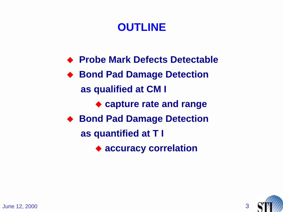
OUTLINE
! Probe Mark Defects Detectable! Bond Pad Damage Detection
as qualified at CM I! capture rate and range
! Bond Pad Damage Detectionas quantified at T I
! accuracy correlation
June 12, 2000 4
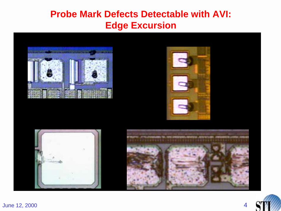
Probe Mark Defects Detectable with AVI:Edge Excursion

June 12, 2000 5
Probe Mark Defects Detectable with AVI:Pad Discoloration
June 12, 2000 6
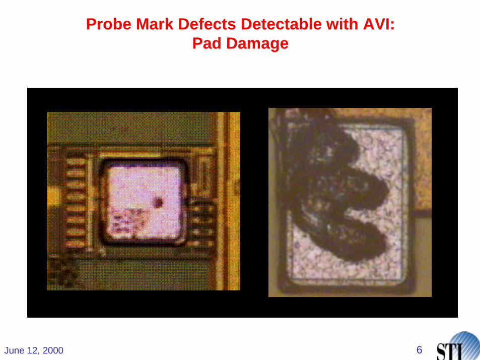
Probe Mark Defects Detectable with AVI:Pad Damage
June 12, 2000 7
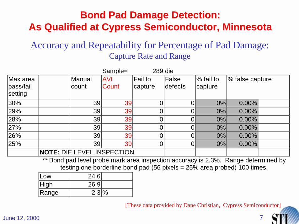
Bond Pad Damage Detection:As Qualified at Cypress Semiconductor, Minnesota
Sample= 289 dieMax areapass/failsetting
Manualcount
AVICount
Fail tocapture
Falsedefects
% fail tocapture
% false capture
30% 39 39 0 0 0% 0.00%29% 39 39 0 0 0% 0.00%28% 39 39 0 0 0% 0.00%27% 39 39 0 0 0% 0.00%26% 39 39 0 0 0% 0.00%25% 39 39 0 0 0% 0.00%
NOTE: DIE LEVEL INSPECTION** Bond pad level probe mark area inspection accuracy is 2.3%. Range determined by
testing one borderline bond pad (56 pixels = 25% area probed) 100 times.Low 24.6High 26.9Range 2.3 %
Accuracy and Repeatability for Percentage of Pad Damage:Capture Rate and Range
[These data provided by Dane Christian, Cypress Semiconductor]
June 12, 2000 8
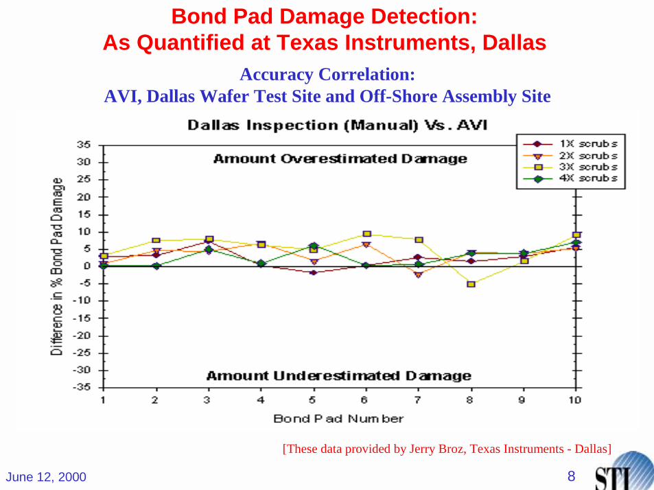
Bond Pad Damage Detection:As Quantified at Texas Instruments, Dallas
Accuracy Correlation: AVI, Dallas Wafer Test Site and Off-Shore Assembly Site
[These data provided by Jerry Broz, Texas Instruments - Dallas]
June 12, 2000 9
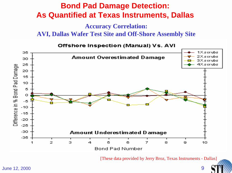
Bond Pad Damage Detection:As Quantified at Texas Instruments, Dallas
Accuracy Correlation: AVI, Dallas Wafer Test Site and Off-Shore Assembly Site
[These data provided by Jerry Broz, Texas Instruments - Dallas]

June 12, 2000 10
Bond Pad Damage Detection:As Quantified at Texas Instruments, Dallas
Accuracy Correlation: AVI, Dallas Wafer Test Site and Off-Shore Assembly Site
[These data provided by Jerry Broz, Texas Instruments - Dallas]
June 12, 2000 11
Part Two:
Implementing AVI into the
Test Floor Production Process
June 12, 2000 12
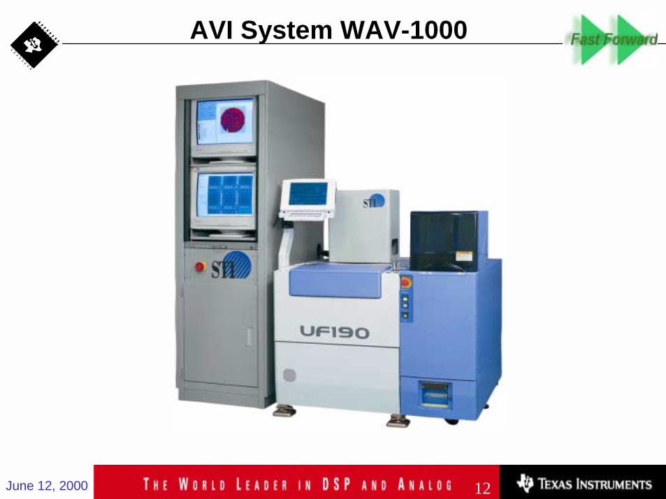
AVI System WAV-1000
12
June 12, 2000 13
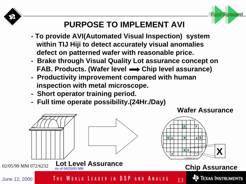
PURPOSE TO IMPLEMENT AVI - To provide AVI(Automated Visual Inspection) system
within TIJ Hiji to detect accurately visual anomaliesdefect on patterned wafer with reasonable price.
- Brake through Visual Quality Lot assurance concept onFAB. Products. (Wafer level Chip level assurance)
- Productivity improvement compared with humaninspection with metal microscope.
- Short operator training period.- Full time operate possibility.(24Hr./Day)
J-1234567-XX-YY
XX
XX
XX
X
X XX
XLot Level Assurance
Wafer Assurance
Chip Assurance02/05/99 MM 072/6232 As of 04/25/00 MM
13
June 12, 2000 14
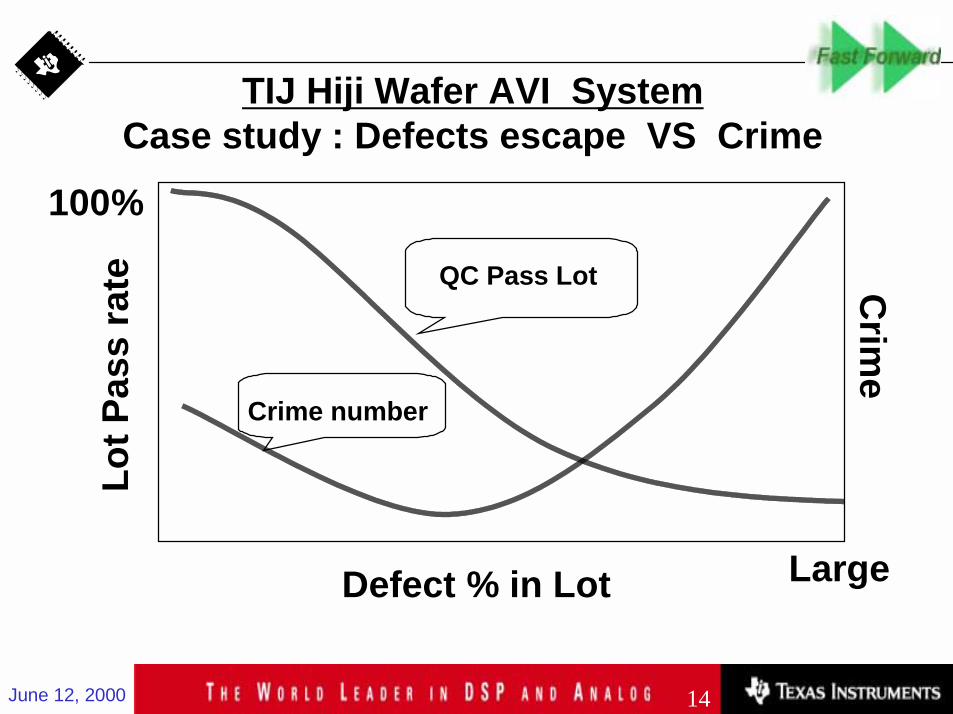
TIJ Hiji Wafer AVI System Case study : Defects escape VS Crime
Lot P
ass
rate
Defect % in Lot
Crim
e
Large
100%
QC Pass Lot
Crime number
14

June 12, 2000 15
TIJ Hiji Wafer AVI System From Assembly line Defect Analysis
Defect size (um)
Def
ectQ
’ty
Large
High Can be detected over 90% defect,if we screening more than targetedsize defects.
15

June 12, 2000 16
TIJ Hiji AVI System SYSTEM DESCRIPTION/DESIGN- Automated Wafer Handling Platform. (Load/Unload, Align,Index or Position)
- Accurate repeatability. (Over 90%)- Speedy inspection time. (Approx. 3 Min./6”Wafer 100% Inspect.)- Minimum 10um defect size detect. - Automatic Defect Categorization is future concept.
As of 04/25/00 MM
16

June 12, 2000
Hiji AVI Current Methodology -1/2• CapabilityFunction
- Defect detection 4 ~ 5um or more >90% repeatability.(Use Sub-Pixel test)- High speed visual inspection. (Approx. 90s /6” W, (225s/6”W with Load/UnLoad))- Multi dies(x2, x3 or xN) and Sub dies(1/2, 1/3 or 1/N) inspect function.- 100% chips/Wafer inspection, random sampling inspection with set AQL level.- Wafer handling size from 5” to 8”.- Motorized optics (SQ 200 mil - 500mil).- Offline ink/Ink Less. - Defect area and size identification and display.- Bond Pad mask.- Auto training and auto start.
- Automatic lot number recognize by OCR.- Device program load for Prober, Mapper or Vision PC.- Auto focus, auto light level adjustment.- Wafer Alignment, reference chip location recognize. - Generate sampling chips for reference chip image shots.
01/18/99-MM- 03/6232 As of 04/25/00 MM
17

June 12, 2000 18
Hiji AVI Current Methodology -2/2
• CapabilityProgramming
- Process area selection or setting- Minimum detect size setting in process area. - Ink chip screening or skip function.- Light level adjustment setting for Inspection VS reference images.- Set Magnification(SQ 200 mil - 500mil).- Specific area setting with filter(set minimum detect size). - Set detect sensitivity(Low, Mid, Hi., 1 - 3 STD DEV.)
Test accuracy technique- Particle wipe off Filtered Air(N2) blow.- Retest mode.- Auto stop for abnormal percentage defect wafer.- AVI fail location display(Wafer map, Chip map) or defect size,.- Review defect location and defect identify by color capture screen.
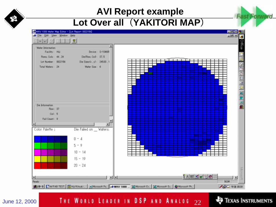
Reporting - Generate overlay, wafer map. (YAKITORI MAP)- Auto print report at any lot operation end .
01/18/99-MM- 03/6232 As of 04/25/00 MM
18

June 12, 2000 19
INK chip Elec.failINK chip Elec.failINK chip Elec.failINK chip Elec.failXXXX Visual failVisual failVisual failVisual fail
AVI System Multi/Sub. Chip inspection
Multi chips inspection
Divided chip part Inspection for big chip
ExExExEx....3x3 chips/1 shot 1/3 chip area/1 shot
XXXX
19

June 12, 2000 20
Example AVI Lot report
20

June 12, 2000
AVI Report Example Each Wafer
21
June 12, 2000
AVI Report exampleLot Over all((((YAKITORI MAP))))
22
June 12, 2000
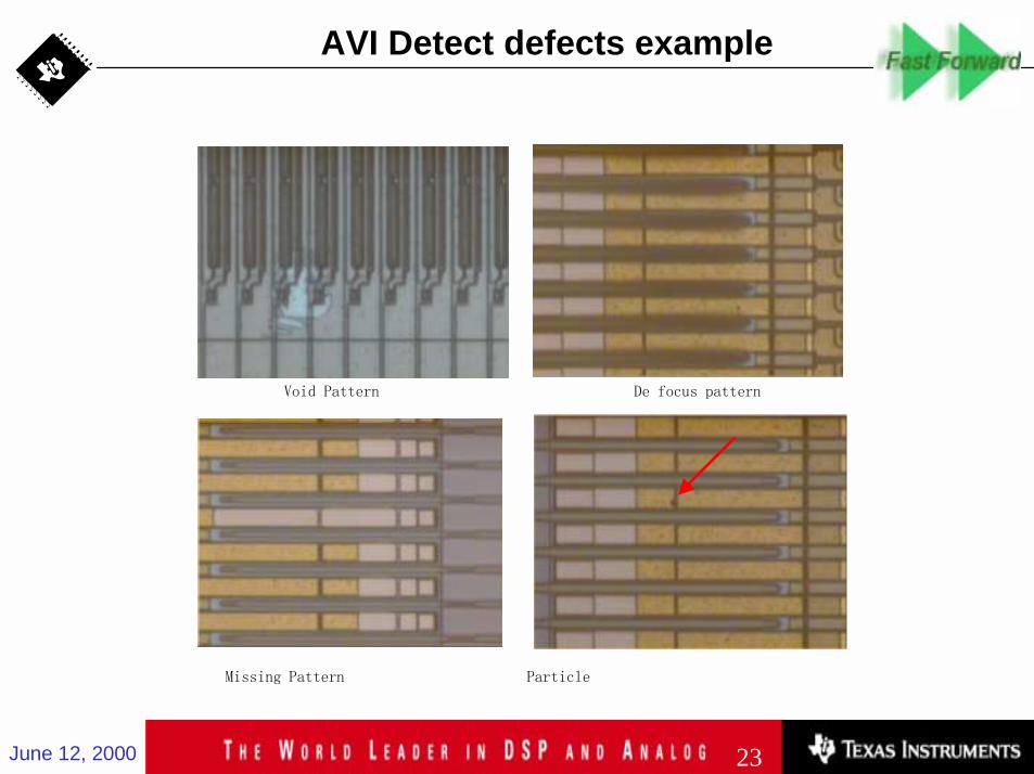
Void Pattern De focus pattern
Missing Pattern
AVI Detect defects example
Particle
23
June 12, 2000
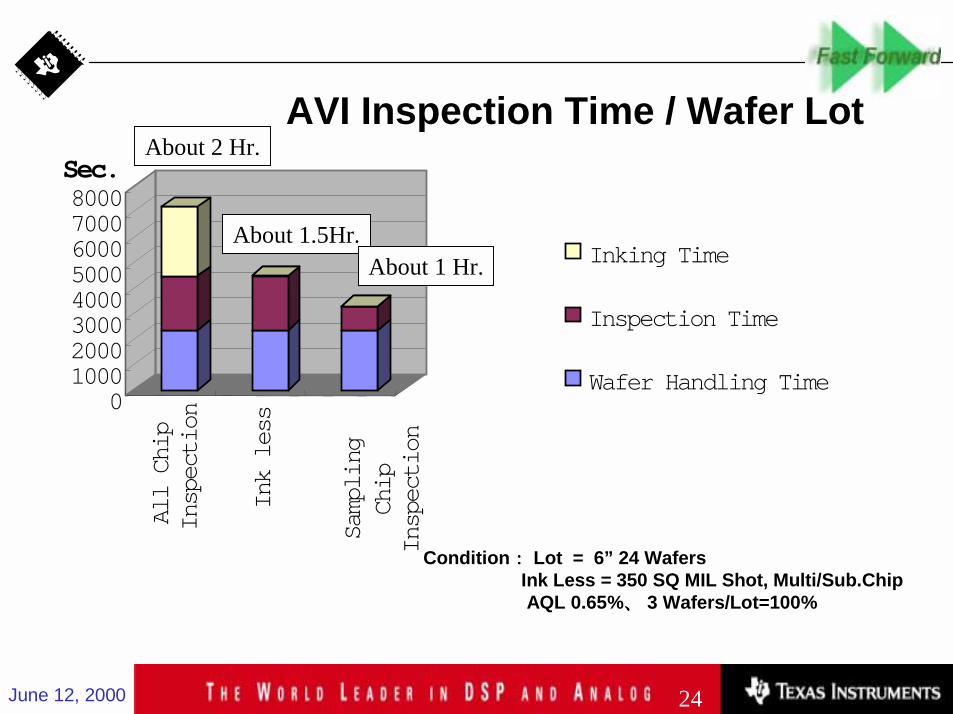
Inking Time
Inspection Time
Wafer Handling Time
Sec.All Chip
Inspection
Ink less
Sampling
Chip
Inspection
AVI Inspection Time / Wafer Lot
010002000300040005000600070008000
About 2 Hr.
About 1.5Hr.About 1 Hr.
Condition:::: Lot = 6” 24 WafersInk Less = 350 SQ MIL Shot, Multi/Sub.ChipAQL 0.65%、、、、 3 Wafers/Lot=100%
24

June 12, 2000
AVI Inspection Defects AnalysisBefore M/P Test on 104227 Device
85%
7% 3%
1%4%
Fab.DefectForeign Material(Metallic)
Grease Contamination
Oil mist Contamination
Do not Identified
Evaluation Lot = 2, n = 67
09/30/98 MM 072/6232
25
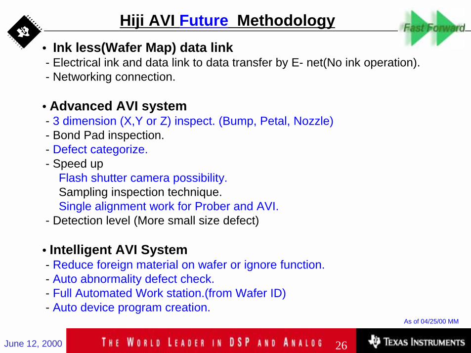
June 12, 2000 26
Hiji AVI Future Methodology• Ink less(Wafer Map) data link- Electrical ink and data link to data transfer by E- net(No ink operation).- Networking connection.
• Advanced AVI system- 3 dimension (X,Y or Z) inspect. (Bump, Petal, Nozzle)- Bond Pad inspection.- Defect categorize.- Speed up
Flash shutter camera possibility.Sampling inspection technique.Single alignment work for Prober and AVI.
- Detection level (More small size defect)
• Intelligent AVI System- Reduce foreign material on wafer or ignore function.- Auto abnormality defect check.- Full Automated Work station.(from Wafer ID)- Auto device program creation.
As of 04/25/00 MM
26
June 12, 2000
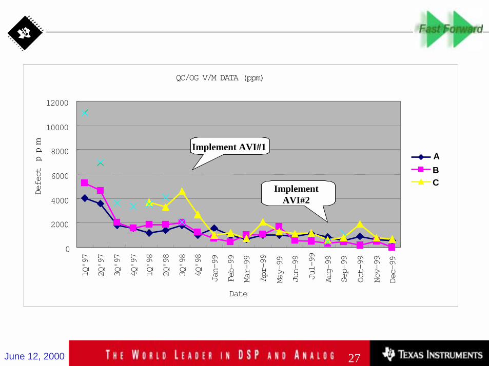
QC/OG V/M DATA (ppm)
0
2000
4000
6000
8000
10000
12000
1Q'97
2Q'97
3Q'97
4Q'97
1Q'98
2Q'98
3Q'98
4Q'98
Jan-99
Feb-99
Mar-99
Apr-99
May-99
Jun-99
Jul-99
Aug-99
Sep-99
Oct-99
Nov-99
Dec-99
Date
Defect ppm
ABC
Implement AVI#1
Implement AVI#2
27
June 12, 2000
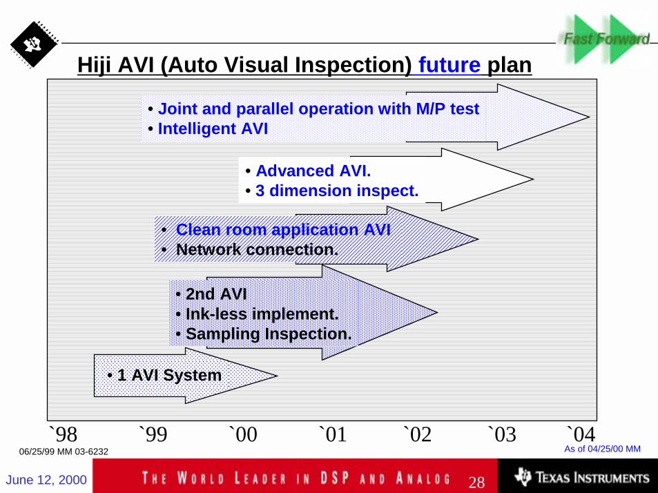
Hiji AVI (Auto Visual Inspection) future plan
• 1 AVI System
• Clean room application AVI• Network connection.
• 2nd AVI• Ink-less implement.• Sampling Inspection.
• Advanced AVI.• 3 dimension inspect.
• Joint and parallel operation with M/P test• Intelligent AVI
06/25/99 MM 03-6232`98 `99 `00 `01 `02 `03 `04
As of 04/25/00 MM
28