Automatic Gain Control In WCDMA Terminals …lup.lub.lu.se/search/ws/files/6335198/625608.pdf ·...
7
Automatic Gain Control In WCDMA Terminals Alriksson, Peter; Bernhardsson, Bo; Lindoff, Bengt Published: 2004-01-01 Link to publication Citation for published version (APA): Alriksson, P., Bernhardsson, B., & Lindoff, B. (2004). Automatic Gain Control In WCDMA Terminals. General rights Copyright and moral rights for the publications made accessible in the public portal are retained by the authors and/or other copyright owners and it is a condition of accessing publications that users recognise and abide by the legal requirements associated with these rights. • Users may download and print one copy of any publication from the public portal for the purpose of private study or research. • You may not further distribute the material or use it for any profit-making activity or commercial gain • You may freely distribute the URL identifying the publication in the public portal Take down policy If you believe that this document breaches copyright please contact us providing details, and we will remove access to the work immediately and investigate your claim.
Transcript of Automatic Gain Control In WCDMA Terminals …lup.lub.lu.se/search/ws/files/6335198/625608.pdf ·...

LUND UNIVERSITY
PO Box 117221 00 Lund+46 46-222 00 00
Automatic Gain Control In WCDMA Terminals
Alriksson, Peter; Bernhardsson, Bo; Lindoff, Bengt
Published: 2004-01-01
Link to publication
Citation for published version (APA):Alriksson, P., Bernhardsson, B., & Lindoff, B. (2004). Automatic Gain Control In WCDMA Terminals.
General rightsCopyright and moral rights for the publications made accessible in the public portal are retained by the authorsand/or other copyright owners and it is a condition of accessing publications that users recognise and abide by thelegal requirements associated with these rights.
• Users may download and print one copy of any publication from the public portal for the purpose of privatestudy or research. • You may not further distribute the material or use it for any profit-making activity or commercial gain • You may freely distribute the URL identifying the publication in the public portalTake down policyIf you believe that this document breaches copyright please contact us providing details, and we will removeaccess to the work immediately and investigate your claim.

Download date: 10. Sep. 2018

AUTOMATIC GAIN CONTROL IN WCDMA TERMINALS
1Peter Alriksson, 2Bo Bernhardsson and 2Bengt Lindoff
1Department of Automatic Control, Lund Institute of Technology
Box 118, 221 00 Lund, Sweden2Research Department, Ericsson Mobile Platforms AB
Nya Vattentornet, 221 83 Lund, Sweden
Abstract This article gives a presentation of the Automatic Gain Control
algorithm used in WCDMA (3rd generation mobile networks). The focus is
on how the controller bandwidth influences settling times and modulation
distortion. This will be investigated through simulation for two different
channel cases.
Keywords AGC, Automatic Gain Control, WCDMA , UMTS
1. INTRODUCTION
The purpose of this article is to present an in
dustrial application of control theory, namely
Automatic Gain Control (AGC). The AGC is
used on the terminal side in the 3rd genera
tion mobile network, from here on referred to
as WCDMA. The control design presented in
this article was developed at Ericsson Mobile
Platforms in Lund before this project. The pur
pose of this project was to develop a simulator
and to study how different AGCparameters in
fluence the receiver performance. In this arti
cle the tradeoff between settling time after a
step change in received power and modulation
distortion will be investigated through simula
tions. The design parameter is the controller
bandwidth. There are many other parameters
related to AGC that influence overall system
performance. For more simulation results see
(2).
2. A BASIC WCDMA SYSTEM
To be able to understand the function of the
AGC and why it is used, a brief overview of the
communication from base station to terminal in
a simplified WCDMA system will be given.
The information bits are first coded and inter
leaved to reduce the effects of bit errors. This
operation results in a new bit steam. The next
step is to map groups of bits to symbols in
the complex space, typically four (QPSK) or 16
(16QAM) different symbols are used. The se
quence is then multiplied as complex numbers
with a complex pseudo random sequence, the
spreading sequence. Each new symbol after the
multiplication is called a chip. The chip rate in
WCDMA is fixed to 3840000 chips/s. A com
mon unit is a slot that is defined as 2560 chips.
Next the new complex sequence is mapped to
two analog signals ,I(t) and Q(t), and I/Q mod
ulated as
sH F(t) = I(t)√
2 cos(2π fct) − Q(t)√
2 sin(2π fct).(1)
The carrier down link (from base station to
terminal) frequencies, fc, in WCDMA range
from 2110 MHz to 2170 MHz.
On the receiver side the signal is demodulated,
filtered through the same filter as in the trans
mitter and finally AD converted. Because of the
strong variations of received power, the AD
converter (ADC) has to have a large dynamic
range. This is not power and cost effective, and
thus a series of variable gain amplifiers are in
serted before the AD conversion stage. For a de
tailed description of digital communication the
ory see (1).
3. AUTOMATIC GAIN CONTROL
As mentioned in Section 2 the main function
of the AGC is to limit the dynamic range of
the AD converter. To achieve this the AGC
must have a large dynamic range and a fast
settling time after step changes in received
power. According to the 3G specifications (see
(3)) the receiver must be able to handle signal
levels between 106.7dBm and 25dBm. A step
in received power occurs for example when the
WCDMA receiver makes measurements on the
signal quality from neighboring base stations.
One possible scenario is that a neighboring base
station is transmitting at a different carrier
frequency. The I/Q demodulator then changes
carrier frequency for a short period of time,
which leads to an abrupt change in received
power. To minimize the measuring time, the
AGC must compensate for the new received
power as fast as possible.
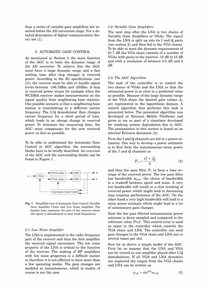
To be able to understand the Automatic Gain
Control or AGC algorithm, the surrounding
blocks have to be briefly described. An overview
of the AGC and the surrounding blocks can be
found in Figure 1.
VGA chain
VGA chain
LNA
Automatic Gain Control
yQ
yI
ADC
ADC
u
Fig. 1 Simplified view of Automatic Gain Control, Variable
Gain Amplifier Chain and Low Noise Amplifier. The
dashed lines represent the part of the receiver where
the signal is demodulated to base band frequencies.
3.1 Low Noise Amplifier
The LNA is implemented in the radio frequency
part of the receiver and thus the first amplifier
the received signal encounters. The low noise
property of the LNA is critical to the function
of the receiver. The making of RF amplifiers
with low noise properties is a difficult matter
so therefore it is not efficient to have more than
a few operating modes. The gain changes are
modeled as instantaneous, which in reality of
course is not the case.
3.2 Variable Gain Amplifiers
The next step after the LNA is two chains of
Variable Gain Amplifiers or VGAs. The signal
from the LNA is split up into its I and Q parts
(see section 2) and then fed to the VGA chains.
To be able to meet the dynamic requirements of
81.7 dB the VGA chain consists of a number of
VGAs with gains in the interval 15 dB to 15 dB
and with a resolution of between 0.5 dB and 2
dB.
3.3 The AGC Algorithm
The task of the controller is to control the
two chains of VGAs and the LNA so that the
estimated power is as close to a preferred value
as possible. Because of the large dynamic range
of the VGA chain the desired gain values Ak
are represented in the logarithmic domain. A
control algorithm that performs this task is
presented below. The presented algorithm was
developed at Ericsson Mobile Platforms and
given to me as part of a simulator developed
for studying system degradation due to AGC.
The presentation in this section is based on an
internal Ericsson document (4).First the I and Q channels are fed to a power es
timator. One way to develop a power estimator
is to first form the instantaneous mean power
of the I and Q channels as
P̂y =y2
I + y2Q
2(2)
and then low pass filter P̂y to form a time av
erage of the received power. The low pass filter
has bandwidth ω pow, the choice of bandwidth
is a tradeoff between speed and noise. A very
low bandwidth will result in a slow tracking of
received power which might lead to decreasing
step response performance of the AGC. On the
other hand a very high bandwidth will lead to a
noisy power estimate which might lead to a lot
of unnecessary gain changes.
Next the low pass filtered instantaneous power
estimate is down sampled and compared to the
reference value Pref . This control error is used
as input to the controller which controls the
VGA chain and LNA. The controller can send
gain changes to the VGA chain and LNA one or
several times per slot.
Now let us derive a simple model of the AGC.
First let us assume that the LNA and VGA
can be viewed as one amplifier placed after I/Q
demodulation. If all VGA and LNA dynamics
are neglected the output from the VGA chains
and LNA can be written as
yI,Q = α eβ AkuI,Q (3)
where α and β are constants depending on
the dynamic range of the VGA chain. The
instantaneous power of y can then be written
as
Py = Pu(α eβ Ak)2 (4)where Pu is the instantaneous power of the in
put u. If the time constant of the low pass filter
in the power estimator is much shorter than the
update rate of the controller the dynamics are
reduced to a time delay and the problem can be
viewed as a linear control problem in the log
arithmic domain. Taking the logarithm of (4)gives
log(Py) = log(Pu) + 2β Ak + 2 log(α ) (5)
Using the control structure presented above
the problem can be viewed as a linear control
problem with log(Py) as the measured variable
and Ak as controller output. The process to be
controlled consists of a static gain 2β and a
disturbance log(Pu) + 2 log(α ), see Figure 2.
GR
2β
z −1
2log(α)+log(P )u
log(Py)log(Pref)
Fig. 2 The control problem in the logarithmic domain. The
parameter β represents the LNA and VGA chain.
The measured output Py can then be written as
log(Py) = G1(z) log(Pu) + G2(z) log(Pref ) (6)
where
G1(z) = 1
1 + 2β GR(z)z−1(7)
G2(z) = 2β GR(z)G1(z) (8)
There are two objectives in the choice of G1(z).The AGC should be able to track and compen
sate for variations in Pu and have a low set
tling time after a step change in Pu. This im
plies a high pass structure of G1(z) with cutoff
frequency higher than the speed of the varia
tions in received power. On the other hand the
AGC must not destroy the modulation of the sig
nal. That is, the cutoff frequency must not be
too high. The only requirement on G2(z) is to
be able to keep a constant reference value, this
corresponds to a low pass structure with suf
ficiently high cutoff frequency. Choosing a PI
controller on the form
GR(z) = KP + K I
z − 1(9)
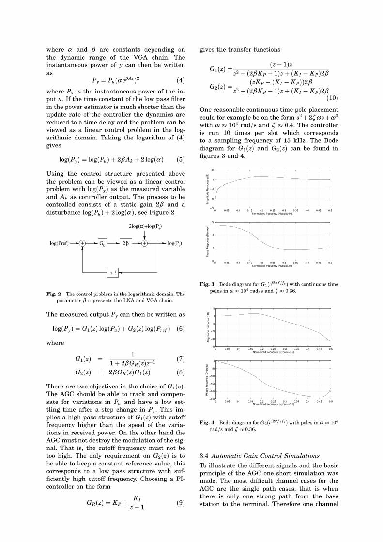
gives the transfer functions
G1(z) = (z − 1)z
z2 + (2β KP − 1)z + (K I − KP)2β
G2(z) = (zKP + (K I − KP))2β
z2 + (2β KP − 1)z + (K I − KP)2β(10)
One reasonable continuous time pole placement
could for example be on the form s2 +2ζ ω s+ω 2
with ω � 104 rad/s and ζ � 0.4. The controller
is run 10 times per slot which corresponds
to a sampling frequency of 15 kHz. The Bode
diagram for G1(z) and G2(z) can be found in
figures 3 and 4.
0 0.05 0.1 0.15 0.2 0.25 0.3 0.35 0.4 0.45 0.5−60
−40
−20
0
20
Normalized frequency (Nyquist=0.5)
Magnitude R
esponse (
dB
)
0 0.05 0.1 0.15 0.2 0.25 0.3 0.35 0.4 0.45 0.5−50
0
50
100
Normalized frequency (Nyquist=0.5)
Phase R
esponse (
Degre
es)
Fig. 3 Bode diagram for G1(ei2π f / fs ) with continuous time
poles in ω � 104 rad/s and ζ � 0.36.
0 0.05 0.1 0.15 0.2 0.25 0.3 0.35 0.4 0.45 0.5−40
−30
−20
−10
0
10
Normalized frequency (Nyquist=0.5)
Magnitude R
esponse (
dB
)
0 0.05 0.1 0.15 0.2 0.25 0.3 0.35 0.4 0.45 0.5−250
−200
−150
−100
−50
0
Normalized frequency (Nyquist=0.5)
Phase R
esponse (
Degre
es)
Fig. 4 Bode diagram for G2(ei2π f / fs ) with poles in ω � 104
rad/s and ζ � 0.36.
3.4 Automatic Gain Control Simulations
To illustrate the different signals and the basic
principle of the AGC one short simulation was
made. The most difficult channel cases for the
AGC are the single path cases, that is when
there is only one strong path from the base
station to the terminal. Therefore one channel

case (VB120) with one path corresponding to
a vehicle velocity of 120 km/h was simulated
for 30 slots using 16QAM modulation. To only
highlight the effects of AGC the channel was
simulated without noise. In Figure 5 the real
part of the input to the AGC together with the
real part of the AD converted output is shown.
The power estimate, AGC gain output and bit
errors are also given.
0 5 10 15 20 25 30−0.2
0
0.2
Re(u
)
0 5 10 15 20 25 30−20
0
20
Re(y
)
0 5 10 15 20 25 3020
30
40
Gain
[dB
]
0 5 10 15 20 25 300
50
100
Phat
0 5 10 15 20 25 300
1000
2000
Bit E
rrors
Slot
Fig. 5 Real parts of input and output together with power
estimate gain output and bit errors. 1 path channel
model corresponding to a vehicle velocity of 120 km/h.
Control design with ω � 104 rad/s.
In Figure 5 the terminal is traveling at a
velocity of 120 km/h. The output from the AGC
seems to be saturated at all times, but this is
not the case. Because of the large amount of
data points plotted the signal looks saturated.
3.5 AGC Step Response Evaluation
To gain a further understanding of the AGC
problem two step response simulations were
made (see figures 6 and 7). The step response
was created by multiplying the incoming signal
with a constant corresponding to the desired
step amplitude. In the simulations a positive
and negative step of 40 dB was used. The AGC
algorithm is implemented so that when the LNA
changes value the VGA chain must change the
gain in the opposite direction to maintain the
same gain level.
One observation that can be made is that the
positive step response is faster than the nega
tive. If we assume a 4 bit AD converter, the dis
crete power levels range between 1 and 225. The
reference value used in this simulation is 35.
The controller works in the logarithmic domain
which implies that the maximum differences be
tween desired power and the current power are
15 dB and 8 dB respectively. For a positive 40
dB step, the power level saturates at 1, which
leads to a difference of 15 dB. For a negative
4 5 6 7 8 9 100
20
40
60
Slots
Tota
l G
ain
dB 10rad/s
20rad/s30rad/s
4 5 6 7 8 9 100
20
40
Slots
VG
A G
ain
dB
4 5 6 7 8 9 10−20
0
20
Slots
LN
A G
ain
dB
4 5 6 7 8 9 100
100
200
300
Slots
Pow
er
Estim
ate
Fig. 6 Negative step of 40 dB at t=5 slots for three
different AGC designs. All controllers have relative
damping ζ = 0.36. The AGC algorithm is implemented
so that when the LNA changes value the VGA chain
must change the gain in the opposite direction to
maintain the same gain level.
14.5 15 15.5 16 16.5 17 17.5 18 18.5 190
20
40
60
Slots
Tota
l G
ain
dB 10rad/s
20rad/s30rad/s
14.5 15 15.5 16 16.5 17 17.5 18 18.5 190
20
40
60
Slots
VG
A G
ain
dB
14.5 15 15.5 16 16.5 17 17.5 18 18.5 19−20
0
20
Slots
LN
A G
ain
dB
14.5 15 15.5 16 16.5 17 17.5 18 18.5 190
20
40
60
Slots
Pow
er
Estim
ate
Fig. 7 Positive step of 40 dB at t=15 slots. The positive
step is faster than the negative one in Figure 6. If we
assume a 4 bit AD converter, the discrete power levels
range between 1 and 225. The reference value used
in this simulation is 35. The controller works in the
logarithmic domain which implies that the maximum
differences between desired power and the current
power are 15 dB and 8 dB respectively. For a positive
40 dB step, the power level saturates at 1, which leads
to a difference of 15 dB. For a negative step of 40 dB the
power level saturates at 225 which gives a difference
of 8 dB and thus leads to less control action than the
positive step.
step of 40 dB the power level saturates at 225
which gives a difference of 8 dB and thus leads
to less control action than the positive step.
From the step response simulations we can
draw the conclusion that a faster controller is
preferable to a slower one.
4. BIT ERROR SIMULATIONS
In this section two bit error simulations were
made, one with a channel model corresponding

to a pedestrian walking at 3 km/h (PA3) and the
VB120 channel used in section 3.4. To be able to
calculate the raw bit error, 2.56 ⋅ 106 bits where
fed through the simulator and the bit error was
calculated for different signal to noise ratios.
The modulation technique used in this section
is 16QAM. For a more detailed description of
the different channel cases and other simulation
parameters see (2).
As can be seen in Figure 8 the fastest AGC gives
the worst bit error, whereas the two slower ones
are almost equal in performance. In Figure 9 on
the other hand, the worst bit error rates where
achieved with the slowest controller. One obser
vation is that the 2 ⋅ 104 rad/s controller gives
good performance in both cases. The choice of
optimal controller bandwidth is thus dependent
on the channel model. If the variations in re
ceived power are slow a fast controller will only
degrade performance and thus a slow controller
is preferred. On the the hand, if the variations
are very fast a faster controller is preferred. But
increasing the bandwidth from 2 ⋅ 104 rad/s to
4 ⋅ 104 rad/s seems to give a very small perfor
mance gain.
0 2 4 6 8 10 12 14 16 18 2010
−2
10−1
100
SNR dB
BE
R
2⋅104 rad/s
1⋅104 rad/s
4⋅104 rad/s
Fig. 8 Bit error for a typical pedestrian channel model
for different signal to noise ratios. A faster controller
degrades performance.
5. CONCLUSIONS
Because the pedestrian channel model is a
more likely setting, it seems that a slower
AGC design is preferred when compared to a
faster one with respect to bit error rate. In
the step response simulations however a faster
AGC design is preferable. What controller to
choose thus depends on the requirements of the
step response and the most probable reception
environment.
2 4 6 8 10 12 14 16 18 2010
−2
10−1
SNR dB
BE
R
2⋅104 rad/s
1⋅104 rad/s
4⋅104 rad/s
Fig. 9 Bit error for a vehicle channel model for different
signal to noise ratios. A faster controller increases
performance up to a certain point
REFERENCES
[1] John G. Proakis. Digital Communications
McGrawHill, 1995.
[2] Peter Alriksson. Automatic Gain Control
in High Speed WCDMA Terminals Mas
ters thesis ISRN LUTFD2/TFRT–5691–
SE, September 2002. Department of Auto
matic Control, Lund Institute of Technol
ogy, Lund, Sweden.
[3] 3rd Generation Partnership Project. 3GPP
TS 25.101 V3.9.0 (200112)
[4] Internal Ericsson Report