
Auto-Zeroing Baseline Compensation for Chemical Sensor ...skennoch.net/MSEEThesis_2002.pdfand...
84
Auto-Zeroing Baseline Compensation for Chemical Sensor Signal Extraction Sam McKennoch A thesis submitted in partial fulfillment of the requirements for the degree of Master of Science in Electrical Engineering University of Washington 2002 Program Authorized to Offer Degree: Electrical Engineering
Transcript of Auto-Zeroing Baseline Compensation for Chemical Sensor ...skennoch.net/MSEEThesis_2002.pdfand...
Auto-Zeroing Baseline Compensation for Chemical Sensor Signal Extraction
Sam McKennoch
A thesis submitted in partial fulfillment of the requirements for the degree of
Master of Science in Electrical Engineering
University of Washington
2002
Program Authorized to Offer Degree: Electrical Engineering


University of WashingtonGraduate School
This is to certify that I have examined this copy of a master’s thesis by
Sam McKennoch
and have found that it is complete and satisfactory in all respects,and that any and all revisions required by the final
examining committee have been made.
Committee Members:
________________________________________________Denise Wilson
________________________________________________Bruce Darling
Date: __________________


In presenting this thesis in partial fulfillment of the requirements for a Master’s degree atthe University of Washington, I agree that the Library shall make its copies freely avail-able for inspection. I further agree that extensive copying of this thesis is allowable onlyfor scholarly purposes, consistent with “fair use” as prescribed in the U.S. Copyright Law.Any other reproduction for any purposes or by any means shall not be allowed without mywritten permission.
Signature________________________
Date ___________________________

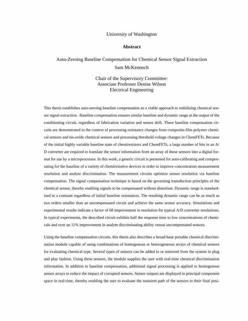
University of Washington
Abstract
Auto-Zeroing Baseline Compensation for Chemical Sensor Signal Extraction
Sam McKennoch
Chair of the Supervisory Committee:Associate Professor Denise Wilson
Electrical Engineering
This thesis establishes auto-zeroing baseline compensation as a viable approach to stabilizing chemical sen-
sor signal extraction. Baseline compensation ensures similar baseline and dynamic range at the output of the
conditioning circuit, regardless of fabrication variation and sensor drift. These baseline compensation cir-
cuits are demonstrated in the context of processing resistance changes from composite-film polymer chemi-
cal sensors and tin-oxide chemical sensors and processing threshold voltage changes in ChemFETs. Because
of the initial highly variable baseline state of chemiresistors and ChemFETs, a large number of bits in an A/
D converter are required to translate the sensor information from an array of these sensors into a digital for-
mat for use by a microprocessor. In this work, a generic circuit is presented for auto-calibrating and compen-
sating for the baseline of a variety of chemiresistive devices in order to improve concentration measurement
resolution and analyte discrimination. The measurement circuits optimize sensor resolution via baseline
compensation. The signal compensation technique is based on the governing transduction principles of the
chemical sensor, thereby enabling signals to be compensated without distortion. Dynamic range is standard-
ized to a constant regardless of initial baseline resistances. The resulting dynamic range can be as much as
two orders smaller than an uncompensated circuit and achieve the same sensor accuracy. Simulations and
experimental results indicate a factor of 68 improvement in resolution for typical A/D converter resolutions.
In typical experiments, the described circuit exhibits half the response time to low concentrations of chemi-
cals and over an 11% improvement in analyte discriminating ability versus uncompensated sensors.
Using the baseline compensation circuits, this thesis also describes a broad-base portable chemical discrimi-
nation module capable of using combinations of homogenous or heterogeneous arrays of chemical sensors
for evaluating chemical type. Several types of sensors can be added to or removed from the system in plug
and play fashion. Using these sensors, the module supplies the user with real-time chemical discrimination
information. In addition to baseline compensation, additional signal processing is applied to homogenous
sensor arrays to reduce the impact of corrupted sensors. Sensor outputs are displayed in principal component
space in real-time, thereby enabling the user to evaluate the transient path of the sensors to their final posi-

tion in principal component space. Visual display of transient behavior is intended to improve usability in
the field of these portable instruments.

TABLE OF CONTENTS
Table of Contents iList of Figures iiiList of Tables v
CHAPTER 1 Introduction...................................................................................................1Sensor Overview .............................................................................................................1Sensor Signal Processing Overview ...............................................................................2Chemical Sensing Applications ......................................................................................4Alternative Methods........................................................................................................5Novelty............................................................................................................................7Thesis Organization ........................................................................................................7
CHAPTER 2 Background ...................................................................................................9Composite-Film Polymer Chemiresistors .......................................................................9Tin-Oxide Chemical Sensors ........................................................................................12ChemFET Chemical Sensors ........................................................................................14Chemical Sensor Noise .................................................................................................16Chemical Sensor Baseline Variance .............................................................................18Chemical Sensor Drift...................................................................................................19
CHAPTER 3 Circuit Design and Experimental Results ................................................21Baseline Compensation Circuit Requirements .............................................................21Manual auto-zeroing baseline compensator..................................................................22Variable-resistor auto-zeroing baseline compensator ...................................................24Discrete Variable-Current Auto-zeroing Baseline Compensator..................................28Integrated Variable-Current Auto-Zeroing Baseline Compensator ..............................34Noise Filtering...............................................................................................................39Comparison of discrete and integrated compensator circuits .......................................40Auto-Zeroing Baseline Compensator Capabilities .......................................................42Impact of Quantization Noise on System Performance ................................................45Homogenous Sensor Arrays..........................................................................................47Interferent Compensation..............................................................................................48
CHAPTER 4 System Integration and Summary ............................................................53Transient Response Chemical Discrimination Module Background............................53Interchangeable Sensor Interface ..................................................................................54Outlier Removal ............................................................................................................56Principal Component Analysis......................................................................................57Experimental Results ....................................................................................................58Suggested future areas of research................................................................................61Summary .......................................................................................................................62
i

ii

LIST OF FIGURES
Figure Number Page
1. Large and Small Signal Models of Carbon-Black Insulating-Polymer Sensors........10
2. A diode-connected ChemFet .....................................................................................14
3. Experimental ChemFET Data....................................................................................15
4. Manual-Zeroing Baseline Compensation Circuit Schematic ....................................22
5. Magnitude Frequency Response for a First-Order Low Pass Filter ..........................23
6. Wheatstone Bridge.....................................................................................................25
7. Variable Resistor Auto-Zeroing Baseline Compensator Compensation Scheme......25
8. Variable-Resistor Auto-Zeroing Baseline Compensator Error..................................27
9. Compensation Feedback Loop ..................................................................................28
10. Output Stage Schematic.............................................................................................29
11. Composite-Film Polymer Chemiresistor During Compensation...............................30
12. Response of Tin-Oxide Sensors to Propanol .............................................................31
13. Normalized Compensated and Uncompensated Response of Tin Oxide Sensors.....32
14. Drift Compensation in a Composite-Film Polymer Chemiresistors..........................33
15. Block Diagram of Integrated Compensation Scheme ...............................................34
16. Integrated Circuit Compensation Process..................................................................35
17. Schematic of Portions of the Integrated Compensation Circuit. ...............................36
18. Current Source Test ...................................................................................................37
19. Drift and Recompensation in a 2610 Tin-Oxide Chemical Sensor ...........................38
20. Compensation Error vs. Baseline Resistance ............................................................39
21. ChemFET Noise ........................................................................................................40
22. Simulation of Compensated and Uncompensated Sensor Response.........................43
23. Quantization Noise of Traditional One-Stage DAC (a) vs. Two-Stage DAC (b) .....46
24. Biologically-Inspired Interferent Rejection Circuit...................................................48
25. Output in Presence of Different Static Levels of Interferent.....................................49
26. Output in Presence of Changing Interferent Levels ..................................................49
27. Effect of Changing Current Source Sizing ................................................................50
iii

28. Measured Compensation of Multiple Sensor Types..................................................55
29. Outlier Removal.........................................................................................................56
30. Principal Component Analysis on Compensated and Uncompensated Sensors .......57
31. Principal Component Analysis Experimental Results...............................................59
32. Sample Module Screen Shot......................................................................................60
33. Transient Response Module ......................................................................................60
iv
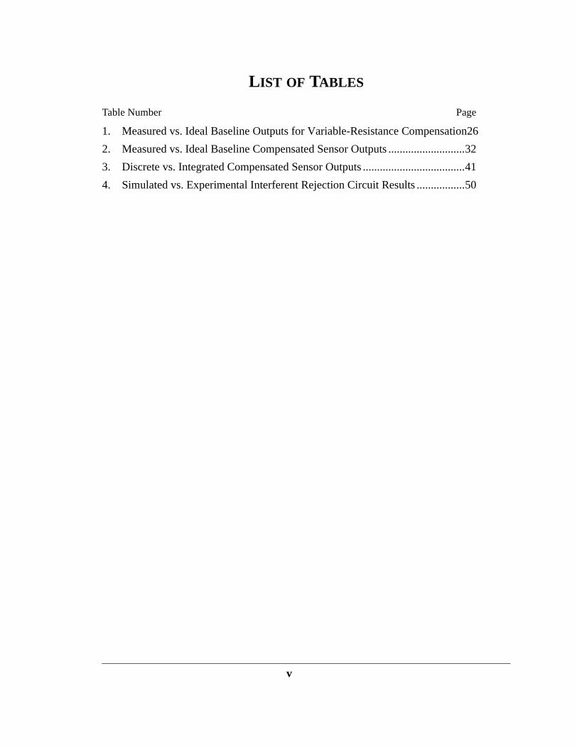
LIST OF TABLES
Table Number Page
1. Measured vs. Ideal Baseline Outputs for Variable-Resistance Compensation26
2. Measured vs. Ideal Baseline Compensated Sensor Outputs ...........................32
3. Discrete vs. Integrated Compensated Sensor Outputs ....................................41
4. Simulated vs. Experimental Interferent Rejection Circuit Results .................50
v

vi

1
CHAPTER 1 Introduction
Chemical Sensors are sensors that typically transduce information in the presence of chemicals
into an electrical signal that can then be processed and interpreted for discrimination, concentra-
tion, and localization information. Many types of chemical sensors have been fabricated over the
past forty years. They include conventional three electrode electrochemical configurations, FET-
based sensors, QCMs (quartz crystal microbalances), and chemiresistors based on Conducting
Polymers, Composite-Film Insulating Polymers and metal oxides. These sensors use a variety of
transduction mechanisms and each have unique advantages and disadvantages that vary with
application. As a cross-section of existing non-optical chemical sensors, this research effort has
concentrated on using three types of chemical sensors, composite-film polymer chemiresistors,
tin-oxide chemiresistors, and ChemFETs. More specifically, this research effort seeks to maximize
extraction of the chemical sensor response signal using intelligent pre-processing and creative sys-
tem integration. The techniques presented in this thesis are demonstrated on a representative set of
chemical sensor technologies and can be used on a wide variety of optical and non-optical chemi-
cal sensing technologies.
SECTION 1.1 SENSOR OVERVIEW
Chemiresistors using composite-film insulating polymers, a relative recent addition to available
chemical sensor technologies, show promise because of high sensitivity and linear response at low

2 Introduction
chemical concentrations of interest. Linear response enables superposition while discriminating
chemicals, greatly simplifying the resolution of analyte mixtures in the sensing environment.
These sensors are also relatively inexpensive, are easy to manufacture, and are easily miniaturized
for use in arrays of chemical sensors. Composite-film polymer chemiresistors are made of an insu-
lating polymer matrix implanted with conductive particles, typically carbon-black [1]. Chemically
induced swelling of the insulating polymer changes conducting paths through the carbon-black
and thereby the resistance of the sensor. Large amounts of swelling produce a non-linear relation-
ship with concentration, as predicted by percolation theory. For typical small-signal use however,
these sensors demonstrate a change in resistance from baseline that is directly linearly proportional
to concentration.
Tin oxide sensors are a member of the metal-oxide family of chemiresistors. The ease of fabrica-
tion of metal-oxide sensors along with their stability have made them popular in the commercial
and research communities [2]. They react with reducing gases in the environment causing a
change in sensor conductivity and resistance [3] [4]. A heating element helps to stabilize the ther-
mal environment and improve sensor sensitivity. Resistance generally decreases from some base-
line value with increased gas concentration. The nature of the input-output relationship in metal-
oxide sensors is an inverse power law. A strong dependence on humidity has further been observed
and characterized [3] [4].
ChemFETs are chemically sensitive field effect transistors. They are easy to integrate into support
circuitry and are inexpensive. Chemically-sensitive gate materials cause the FET threshold voltage
to change in response to certain analytes [5] [6]. Different types of chemFETs can be integrated
onto the chip, including sensors that respond to a primary analyte and its interferents, in order to
improve sensor discrimination capabilities. The nature of the input-output relationship between the
channel voltage in a diode-connected ChemFET (in the saturation region of operation) and analyte
concentration is logarithmic, providing increased resolution at low concentrations of analytes [6].
SECTION 1.2 SENSOR SIGNAL PROCESSING OVERVIEW
By the very nature of their heterogeneity, arrays of chemical sensors can exhibit a wide range of
baseline values, types of outputs (resistance, voltage, etc.), dynamic ranges, and aging effects,

3
which impact system integration. Most of these parameters are artifacts of the manufacturing pro-
cess used to make the sensors and provide little useful information on sensor response. For exam-
ple, the wide range of initial baseline values if not compensated, leads to a very wide range of
possible output values. This large dynamic range, once converted to digital values, causes a
decrease in analyte concentration resolution because most of the dynamic range is consumed by
baseline variation rather than by the sensor response to the analyte. Likewise, as many chemical
sensors age, their baseline values tend to drift at rates of a few percent over a period of months,
further compounding the dynamic range problem and adding further complexities to calibration.
This research effort presents a viable solution to the problems of baseline variance and drift. Com-
pensation methods are discussed which allow all sensors, regardless of the unknown initial base-
line to be compensated to the same initial output value. Subsequent compensations over calibrated
time periods are subsequently possible to decrease the effects of drift.
System integration of heterogeneous arrays of chemical sensors into an inexpensive, mobile chem-
ical measurement unit requires consideration of many factors such as signal conditioning, the abil-
ity to flag broken sensors, and streamlining of signal processing for pattern recognition to suit
portability. Signal conditioning is used to enhance data acquisition, which involves accurate ana-
log to digital conversion of sensor data. In order to maximize the resolution of a mobile unit, base-
line compensation can be used to fuse sensor signals in such a way that sensor dynamic range is
reduced. Flagging broken sensors using statistical outlier removal techniques on homogenous
arrays of sensors allows for a high degree of robustness to sensor failure.
In order to classify chemical analytes of interest, this work uses principal component analysis
(PCA). Principal component analysis is a feature reduction method that transforms multiple-
dimensional data into a vector space in which most variance is contained in the first few principal
component directions. In highly correlated data, higher dimensional principal axes become less
significant [7]. PCA has been used in chemical discrimination applications many times [8] [9]. In
this work, PCA is used to reduce six-dimensional sensor data to two principal component dimen-
sions. These dimensions are then displayed as an interface for the user to make classification deci-
sions. This visual display decreases circuit complexity by using built-in human pattern
classification abilities to make decisions regarding chemical detection based on the visual results
4 Introduction
of PCA. PCA has been typically used as a visual aid in determining the discrimination capability
of an array of chemical sensors and can be interpreted directly through visual observation, trans-
ferred to cluster analysis and discrimination factor analysis for linear signal processing, or used as
a precursor in array design for more non-linear signal processing techniques.
Detection of analytes of interest in the presence of interferents is also an important topic of interest
regarding chemical sensors. A simple integrated biologically-inspired circuit is discussed and
evaluated in this research effort. When used in conjunction with the appropriate types of sensor
arrays and with smart sensor-type choices, this circuit (used for interferent rejection) further
increases the amount of information extracted from these sensors.
SECTION 1.3 CHEMICAL SENSING APPLICATIONS
For chemical vapor monitoring, a clear need exists for a low-power mobile chemical sensing plat-
form capable of detecting a wide variety of chemical analytes and analyte concentrations. Potential
applications include food monitoring (by detecting the outgassing components) [10], indoor air
quality monitoring, and environmental monitoring. Chemical environmental sensing is particularly
important in judging the impact that humans have on the environment. To be effective in the field,
chemical sensing must be carried out in a real-time, distributed, and highly sensitive manner. By
looking at the local effects of atmospheric pollutants, the causes and effects of atmospheric pollu-
tion on the regional and global scale can be better understood. Distributed chemical monitoring of
atmospheric constituents could also potentially improve weather forecasting. In the case of chemi-
cal leaks, it might be useful to monitor the distribution gradient as the leak spreads in order to bet-
ter contain it. A distributed network of the chemical sensors could allow industry to self-monitor
or enable government to cheaply and efficiently monitor industrial pollution emissions in real-
time.
Another category of applications for mobile, low-power distributed chemical sensing is in the area
of indoor air quality monitoring. This category applies to office buildings, factories, and perhaps
even the International Space Station. Currently air quality is being monitored through expensive,
power-hungry techniques such as quadrupole mass spectrometry and ion mobility spectrometry.
While these systems are indeed very accurate, distributed sensing holds many advantages. Due to
5
the inexpensive low-mass nature of distributed sensor arrays, a great deal of redundancy is possi-
ble. A properly optimized sensor array also has the capability to monitor more atmospheric con-
stituents even before being routed into a computer for further analysis. With these sensors
distributed throughout the structure, it would be possible to react to a leak or some other sort of
detriment to the air quality in a very rapid and targeted manner. Intelligent pre-processing of the
chemical sensor signals in essential to realize these schemes in order to reduce the effects of sys-
tematic and random variations within the sensors.
In addition, the recent events of September 2001 have made clear the need for accurate, distrib-
uted, low-power chemical monitoring. In order to better respond to potential acts of terrorism, the
ability to detect potentially hazardous chemicals in a variety of places is extremely important
because the time frame in which actions can be taken to counteract hazardous chemical attacks is
extremely brief [11].
SECTION 1.4 ALTERNATIVE METHODS
A handful of research efforts have demonstrated techniques for improving portable instrument via-
bility by reducing the inherent variation in chemical sensors with baseline compensation tech-
niques. Standard methods using a wheatstone bridge cannot be applied because, for chemiresistors,
the initial resistance varies across manufacturing and lifetime of the sensor. Apsel et al uses an
adaptive, programmable amplifier to stabilize chemiresistors at a predetermined baseline value
using floating gate analog memory and novel filtering techniques. The floating gate capability
allows a continuous range of programmable values, theoretically enabling perfect baseline com-
pensation (within the constraints of transistor performance); however, these circuits also contribute
distortion to the sensor response, generating different response curves for the same analyte, same
type of sensor, but different baseline resistances [12]. Using a different circuit design approach,
Neaves and Hatfield have constructed an ASIC specifically designed to extract response signals
from an array of polymer chemiresistors. This circuit results in fundamental distortion of the sen-
sor signal by creating a non-linear response of the output current in relation to the input concentra-
tion. The ASIC is a versatile generic module for sensor resistance preprocessing, but contains
bulky amplifiers and multipliers that may limit usefulness for large arrays in portable instruments
in terms of space and power consumption [13].

6 Introduction
Many other analyte recognition methods are available besides principal component analysis. For
example, Brezmes et al. use two cascading artificial neural networks, each with one internal hid-
den layer [14]. The first neural network performs analyte identification while the second performs
analyte quantification. The networks also take humidity as an input in order to decrease its effect
on the measurements. While producing good results, this method lacks transparency in that the
way in which the neural network makes the decision is not generally useful in helping the user
determine the accuracy of the result. The results of the neural network are also highly dependant
on the training data used [14].
As mentioned, the interferent rejection circuit employed in this effort helps to improve system
selectivity to desired analytes by taking advantage of the effects of baseline compensation to elim-
inate interferents. Other efforts aimed at interferent rejection have tended to focus on improving
sensor technology. For example, dopant amounts or operating temperature might be varied to alter
selectivity [2]. This effort offers interferent rejection independent of sensor technology as varia-
tions in sensor technology have been compensated for.
One alternate approach to monitor chemical environmental impacts is via satellite observation.
However, most earth-observing satellites acquire mainly image data. For example, the LANDSAT
series of spacecraft acquires detailed images of various places around the world to be compared
with earlier images in order to judge human impact and climate change. Images tell us little about
the chemical composition of air on the ground level and the environmental impact that the chemi-
cal constituents of air can have. Other instruments such as the MOPITT (a gas correlation spec-
troscopy sensor) instrument on the TERRA satellite are optimized to detect only certain gases
(carbon monoxide and methane in this case) and have limited spatial resolution (22km) [15]. Like-
wise, weather stations are not normally distributed in a very dense manner, depending on location.
Also, weather stations are at the present limited in what data they collect (wind speed, temperature
at various depths, and barometric pressure). In addition, weather stations are also limited to taking
data at fixed points. Although, satellites and weather stations have very useful purposes, a clear
need remains for a low-power mobile chemical sensing unit. Previous attempts to build such
7
devices have been limited by a number of factors such as power consumption, the need for a bulky
computer to perform processing, and sensor technology issues like variable baseline and drift.
SECTION 1.5 NOVELTY
The following is a list of the novel components of this thesis:
• A series of discrete and integrated circuits are presented which use a mixed signal method for
sourcing a constant current through a chemiresistor or chemFET in such a way that the sensor
response is not distorted during compensation [16] [17].
• Due to the compensation mechanism used, as previously explained the baseline compensator is
also able to act as a drift compensator. By limiting the dynamic range of a wide variety of sen-
sor types all with different random and systematic variation, baseline and drift compensation
help to enable more mobile low-power applications such as those listed above, all with distort-
ing the sensor signal.
• The integrated circuit presented is the third in a series of integrated baseline circuits for differ-
ent chemical sensor technologies that provides modular baseline-independent compensation
with no distortion of chemical sensor signal. Advantages of the present integrated design over
the discrete circuit include size (a factor of 1310 in reduced volume), cost (a factor of over 40 in
reduced cost per compensated sensor), and accuracy.
• A biologically-inspired interferent rejection circuit is further shown to enhance the detection of
primary analytes in the presence of closely-related interferents.
• The novel approach in this thesis to mobile chemical sensing uses intelligent pre-processing to
enable effective principal component analysis. Human classification abilities can then be taken
full advantage of by displaying PCA data for human interpretation as sensor responses
approach analyte calibration clusters [18]. Similar work on system integration in the literature
tends to concentrate more on odor localization and relies more on theoretical models for inter-
preting sensor data [19].
SECTION 1.6 THESIS ORGANIZATION
8 Introduction
This thesis continues in Chapter 2 with a background on solid-state chemical sensors, including
some of the inherent performance limits. The next chapter discusses multiple aspects of a family of
circuits designed to overcome these intrinsic sensor problems. Chapter 3 also follows up the circuit
design with circuit results, thereby directly demonstrating the ability of these compensation cir-
cuits to better extract chemical sensor information. Chapter 4 discusses the integration of the com-
pensation circuit into higher-level systems and compares performance of these systems to other
pre-existing chemical detection systems. Chapter 4 also suggests possible areas of research that
could use this effort as a starting point, and finally summarizes the main points and results of this
research effort. The circuit and system integration results demonstrate the ability of the presented
circuits to greatly enhance the minimum analyte detection resolution and ability to discriminate
between analytes.
9
CHAPTER 2 Background
As discussed briefly in the introduction, chemical sensors present many challenges to efficient sig-
nal extraction. This chapter begins with a more detailed background on the three sensor technolo-
gies used to demonstrate the circuits in this research: (a) composite-film polymer sensors, (b) tin-
oxide chemiresistors, and (c) chemical field effect transistors (ChemFETs). Following the sensor
descriptions is a detailed analysis of some of the problems associated with successful signal
extraction including the processing of noise, baseline variance and drift.
SECTION 2.1 COMPOSITE-FILM POLYMER CHEMIRESISTORS
Composite-film polymer chemiresistors are a recent entry into the field of chemical sensors. They
have many advantages including that they are inexpensive and easy to manufacture. Composite-
film chemical sensors are chemiresistors made of organic (insulating) polymers implanted with
conductive carbon-black particles. The polymers in the sensors swell reversibly in response to
vapor exposure due to analyte adsorption. Using different organic polymers in different combina-
tions in the manufacture of these sensors, this type of chemiresistor can be made responsive to dif-
ferent types of analytes to varying degrees. When a chemical is applied to which the sensor is to
some degree sensitive, the polymer swells. In swelling, the deposited carbon-black particles are
forced to move farther apart, thereby changing the effective conductivity of the sensor [9]. This
10 Background
change in conductivity can be measured as a resistance and correlated to chemical vapor concen-
tration.
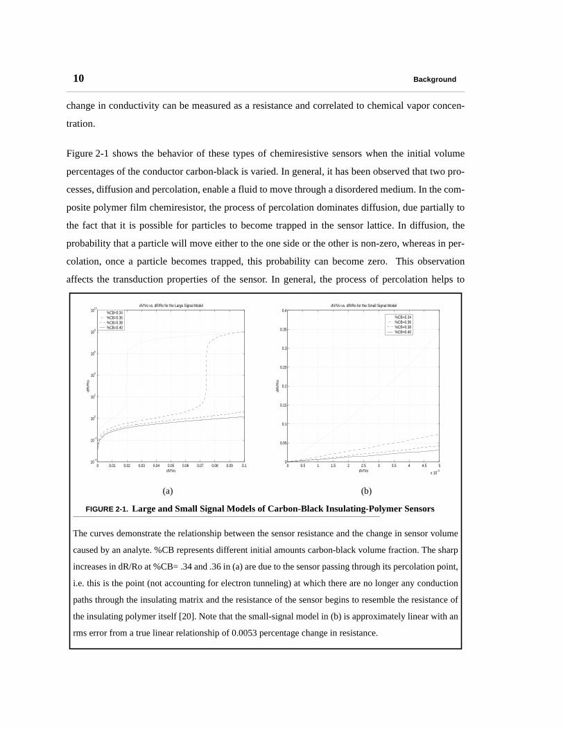
Figure 2-1 shows the behavior of these types of chemiresistive sensors when the initial volume
percentages of the conductor carbon-black is varied. In general, it has been observed that two pro-
cesses, diffusion and percolation, enable a fluid to move through a disordered medium. In the com-
posite polymer film chemiresistor, the process of percolation dominates diffusion, due partially to
the fact that it is possible for particles to become trapped in the sensor lattice. In diffusion, the
probability that a particle will move either to the one side or the other is non-zero, whereas in per-
colation, once a particle becomes trapped, this probability can become zero. This observation
affects the transduction properties of the sensor. In general, the process of percolation helps to
FIGURE 2-1. Large and Small Signal Models of Carbon-Black Insulating-Polymer Sensors
The curves demonstrate the relationship between the sensor resistance and the change in sensor volume
caused by an analyte. %CB represents different initial amounts carbon-black volume fraction. The sharp
increases in dR/Ro at %CB= .34 and .36 in (a) are due to the sensor passing through its percolation point,
i.e. this is the point (not accounting for electron tunneling) at which there are no longer any conduction
paths through the insulating matrix and the resistance of the sensor begins to resemble the resistance of
the insulating polymer itself [20]. Note that the small-signal model in (b) is approximately linear with an
rms error from a true linear relationship of 0.0053 percentage change in resistance.
0 0.5 1 1.5 2 2.5 3 3.5 4 4.5 5
x 10−3
0
0.05
0.1
0.15
0.2
0.25
0.3
0.35
0.4
dV/Vo
dR
/Ro
dV/Vo vs. dR/Ro for the Small Signal Model
%CB=0.34%CB=0.36%CB=0.38%CB=0.40
(a) (b)
0 0.01 0.02 0.03 0.04 0.05 0.06 0.07 0.08 0.09 0.110
−4
10−2
100
102
104
106
108
1010
dV/Vo
dR
/Ro
dV/Vo vs. dR/Ro for the Large Signal Model
%CB=0.34%CB=0.36%CB=0.38%CB=0.40
11
relate the swelling of the sensor as caused by an absorbing analyte to the change in its conductiv-
ity. Initially the resistance of the sensor resembles that of the conductor carbon-black, but as swell-
ing occurs and conduction paths through the carbon-black decrease, the sensor resistance then
approaches that of the insulating polymer. A sharp threshold called the percolation threshold
occurs at which all conduction paths through the carbon-black have disappeared, leading to a sharp
transition in resistance [20] [21]. Assuming only two discrete conductances possible in the sensor
(that of the carbon-black and that of the insulating polymer) a formula for the relationship of the
volume fraction of carbon-black particles to resistance across the composite film may be quanti-
fied using a binomial probability distribution as:
(Eq 2.1)
(Eq 2.2)
(Eq 2.3)
L is the length of the sensor resistor; A is the cross-sectional area of the sensor resistor; z is the
number of conductances connected to each node in the lattice, also known as the coordination
number; f is the packing factor. It ranges from 0.52 for simple cubic spheres to 1 for maximum
packing. is the resistivity of the carbon-black particles while is the resistivity of the insu-
lating polymer. The input to the equation is , the volume fraction of carbon-black particles.
Many other factors have also been known to affect swelling and likewise resistance changes
including temperature, humidity, pressure, and electron tunneling [20] [21]. The percolation prop-
erties of composite-film sensors help to create highly-sensitive sensors that are responsive to many
different types of analytes. However, the added complexity in the manufacturing of these sensors
compared to simple conducting polymer sensors allows for more systematic and random manufac-
turing variations; thus, the initial baseline resistances of this type of sensor covers a broad range
and is dependent on such factors as the type of insulating polymer used, and the initial volume
fraction of carbon-black, thus making transduction of the sensor signal to a useable form difficult.
The sensor response becomes less and less reversible as it is pushed beyond the percolation thresh-
old. Normally, these sensors would be operated at low chemical concentrations where there is a
RLA--- z 2–( )ρcρm
B C B C+( )22 z 2–( )ρcρm+[ ]
1 2⁄+ +
---------------------------------------------------------------------------------------------=
B ρc 1– z 2⁄( ) 1 vc f⁄( )–( )+[ ]=
C ρm zvc 2f⁄( ) 1–[ ]=
ρc ρm
vc
12 Background
fairly linear relation between the chemical concentration and sensor resistance. The small-signal
response of this type of sensor may be characterized by [22]:
(Eq 2.4)
Ro is the baseline sensor resistance; R is the change in resistance from the baseline; [C] is the
applied vapor concentration, typically in ppm; k is a sensor constant. This equation demonstrates
that the baseline value of resistance does not affect the slope of the response curve, as only k
affects the slope. k may change with % Carbon-Black and polymer film thickness, but these factors
are not considered here. k does depends on the chemical applied and the type of polymer being
used. Examples of the value of k are 0.00004 PPM-1 with the polymer poly(ethylene oxide) and
applied chemical cyclohexane, and a value of 0.0008 PPM-1 with the polymer poly(carbonate
bisphenol A) and applied chemical toluene [22].
SECTION 2.2 TIN-OXIDE CHEMICAL SENSORS
Tin-oxide chemiresistors, unlike composite-film polymer chemiresistors and ChemFETs have
been commercially available for some time, and are arguably responsible for saving lives in Japan
by alerting users to potentially dangerous natural gas leaks. Tin-oxide is an n-type semiconducting
metal oxide whose conductivity properties are highly sensitive to gases present in the environ-
ment. The primary reaction in the sensor to analytes is a reduction one, although chemisorption has
also been shown to have an effect [3]. In the redox reaction, oxygen in the environment first inter-
acts via dangling bonds with the sensor surface or grain boundary, extracting electrons and thereby
creating a substantial depletion region [2]. Reducing gases in the environment then combine with
oxygen in the thin film to enable the change in sensor conductivity and resistance by reinjecting
electrons and decreasing the depletion region [3] [4]. It is important that oxygen saturates the sen-
sor prior to introduction of a reducing gas in order to isolate the two effects. In part, because of this
non-selective reaction to reducing gases, tin-oxide chemiresistors exhibit poor selectivity. These
sensors do, however, show excellent stability, are fairly straightforward to fabricate and are moder-
ately compatible with standard IC fabrication methods [2].
∆RRo------- k C[ ]=
∆

13
Other issues associated with tin-oxide sensors include sensor response speed and sensitivity to
temperature. When an analyte is applied, response speeds vary with chemical concentration. The
higher the analyte concentration, the faster the response because the oxygen on the film is com-
bined with more quickly. This reduction in response time can reduce the response time from sev-
eral minutes to only seconds. However, when the analyte is removed, the response time to return
steady-state is constant because the partial pressure of oxygen is constant [3].
Due to the transduction mechanism employed by tin-oxide sensors, sensitivity to different analytes
is highly dependant on sensor temperature. The sensors employed in this research effort maintain a
constant temperature by using a heater filament, thus also stabilizing sensitivity to analytes. This
stability comes at the cost of increased power consumption as a large amount of power is dissi-
pated as heat.
The input-output equation may stated as below:
(Eq 2.5)
a is a sensitivity coefficient; r is a power law exponent for oxides. A strong dependence on oxygen
partial pressure and humidity has further been observed and characterized [3] [4]. For oxygen par-
tial pressure:
(Eq 2.6)
In the case of humidity, water vapor in the air has been shown to act as an electron donor gas,
forming surface hydroxyl groups, thus decreasing sensor resistance. Humidity affects sensitivity to
different analytes differently due to the way various analytes and water vapor react [3].
Although these sensors are much more widely used, problems with signal extraction has limited
their commercial largely to binary triggers of toxic gas levels. As discussed above, the initial base-
line resistance and subsequent drift of these sensors is highly effected by many environmental
parameters such as humidity and temperature, thus creating difficulty in reliably and consistently
extracting the chemical sensor signal.
1R--- 1
Ro------ a C[ ] r
+=
1R--- PO2
0.5–∝

14 Background
SECTION 2.3 CHEMFET CHEMICAL SENSORS
ChemFETs are a member of FET based chemical sensors that also includes ISFETs (Ion-selective
FET) and ENFETs (enzyme FET). Unlike ISFETs and ENFETs, ChemFETs have a conductive
gate, thereby eliminating the need for a large reference electrode and enabling ChemFETs to be
more easily integrated and miniaturized into support circuitry [2]. The gate material, generally a
heavily-doped conducting polymer, is applied on a standard gate oxide. When a chemical is
applied to which the gate material is sensitive, the fermi level at the gate shifts causing a change in
the work function of the metal changes via bulk and surface modulation thereby causing the
threshold voltage of the FET to change in a measurable way [5] [6]. Typically, ChemFETs are
diode-connected as shown in Figure 2-2 where the gate is hardwired to the drain. This connection
helps ensure that the transistor is in the saturation region of operation so long as the gate to source
voltage is greater than the FET threshold voltage. Although research continues to define the funda-
mental behavior of the ChemFET, the basic input-output relationship of a diode-connected Chem-
FET with a constant drain-source current applied can be modelled as:
(Eq 2.7)
x0 and x1 are constants which depend physical device parameters associated with the materials
used to build the ChemFET and the geometry of the device as well. They do not change in a mean-
ingful way in response to an applied analyte and can be determined empirically. a is a scaling fac-
tor. [C] is the concentration of the analyte; ID is the drain current through the ChemFET. It is
generally set to some constant value during signal extraction. k’ is another physical parameter
dependent on the per unit area gate capacitance and electron mobility in the device; W and L are
the width and length of the FET channel. The nature of the input-output equation is then logarith-
FIGURE 2-2. A diode-connected ChemFet
Drain
Gate
Source
Vo xo a C[ ]( ) x1
2ID
k' W L⁄( )---------------------+ +ln=

15
mic. However, this formula is only valid for a certain range of concentrations, a moderate range
where at certain concentrations above and below this range the above relationship does not apply
[6]. Figure 2-3 shows initial verification of this input-output relationship model for a ChemFET.
The relationship between output voltage and the log of analyte concentration is approximately lin-
ear over a broad middle range of concentrations as expected.
A further factor affecting compensation in the case of the ChemFETs is the transient settling time.
For the purposes of this discussion, settling time is the time it takes for the ChemFET to arrive to
within 0.1% of its final value after a constant current has been applied through it, in the absence of
any analyte. A regular FET of this size should have a settling time of a maximum of a few nano-
seconds [23], however certain peculiarities of the ChemFET fabrication process tend to greatly
extend the settling time. In the fabrication of typical Aluminum-gate MOSFETs the final step is to
anneal the aluminum, however this step cannot be performed in ChemFETs due to the modified
gate materials used, instead ChemFETs must be allowed to fully warm up to counteract this initial
drift. Settling times on the order of many minutes have been observed.
ChemFET technology is still being adjusted to produce more robust sensors. One of the current
problems associated with fabrication, the transient settling time, creates problems in that the range
FIGURE 2-3. Experimental ChemFET Data
Preliminary verification of theoretical ChemFET model
using 961 measurements at each of four different
ammonia concentrations, 150, 500, 1500, and 5000
ppm. RMS error of the predicted best-fit line is 3.7 mV.
102
103
104
3.85
3.9
3.95
4Experimental Data from ChemFET in Response to Ammonia
Ammonia Concentration (ppm)
Sens
or O
utpu
t Vol
tage

16 Background
across which the sensor settles creates an enlarged sensor dynamic range, thus reducing the resolu-
tion to which analytes might normally be measured.
SECTION 2.4 CHEMICAL SENSOR NOISE
All sensing systems experience noise of various types. Noise is an important factor affecting
chemical sensor behavior, because transduction relies on an actual chemical surface reaction. This
reaction is by nature a random process and therefore subject to noise. In certain cases noise infor-
mation can be useful, and may even be an indicator of sensor health [24]. However, in general,
noise serves to limit the resolution to which analyte resolution can be measured by increasing the
uncertainty in measurements. It is therefore important to understand how noise affects various
types of chemical sensors before presenting a solution. The following is a discussion of various
noise types that exist in the context of how they affect the sensors described here.
Thermal Noise: Thermal noise is caused by the random motion of electrons in response to thermal
excitation and applies to all materials operating above . This form of noise is especially trou-
blesome in resistors because resistors tend to be high consumers of power which generates heat
thereby increasing electron thermal velocity and the associated thermal noise. Thermal noise is
independent of frequency of operation [25]. For resistors, the rms value of the thermal noise may
be calculated as:
(Eq 2.8)
k is boltzman’s constant; T is the temperature is degrees Kelvin; R is the resistance value; f is the
bandwidth of the circuit into which the sensor is placed. For example, an rms noise voltage value
for a 100k resistor at room temperature in a circuit with a 10MHz bandwidth is 129 V. In
chemiresistors the dominant noise type is thermal [9] [26].
Shot Noise: Shot noise arises due to the fact that current is not a continuous rate of flow of carriers;
a single electron has a finite amount of charge. This discrepancy between a discrete and a continu-
ous flow is especially noticeable at low frequencies. Bipolar junction transistors exhibit high
amounts of shot noise. This high amount of noise is present because the time of arrival of carriers
as they diffuse and drift to the collector-base junction is a random process. For a bipolar junction
0°K
v2
4kTR∆f=
∆
Ω µ
17
transistor in a circuit of bandwidth 10MHz and base current of 100mA, the rms current noise is
0.57 A. Shot noise is also present in field-effect transistors, such as ChemFETs, but is only asso-
ciated with the gate leakage current and can be neglected relative to more dominant types of noise
because the gate leakage current in MOS devices is very near zero [25]. Shot noise therefore does
not play a large role in the types of chemical sensors considered here.
Flicker Noise: Flicker noise is also known as 1/f noise, because it exhibits an inverse relationship
with frequency. This type of noise is caused by the interaction of electrons with surface and inter-
face states where electrons can sometimes become trapped for longer periods of time than else-
where in the material. This trapping mechanism produces noise at frequencies typically below a
few kHz, although this boundary can be much higher. Flicker noise is a particular problem in field
effect transistor structures, because electrons are accelerated through a high electric field through
the channel of the transistor and electron traps in the interface between the channel and insulating
layer between channel and gate have a significant effect on the net flow of electrons through this
shallow channel underneath the gate. Device constants used in the calculation of flicker noise can
vary greatly due to random crystal imperfections associated with the manufacturing process. For a
FET with a DC drain current of 1mA, operating frequency of 1kHz, and circuit bandwidth of
1MHz, the rms drain current noise due to flicker is approximately 1 A rms [25].
Burst Noise: Burst noise is low frequency noise. It is not fully understood and may be correlated
with heavy-metal ion contamination. This type of noise can cause hump-like protrusions in the fre-
quency spectrum. The method of production used determines whether this noise is present. This
type of noise does not appear to play a large part in the types of sensors discussed here [25].
Avalanche Noise: Avalanche noise occurs in zener diodes and avalanche junctions. This type of
noise is caused when carriers in a highly reversed-biased pn junction gain sufficient energy to
cause impact-ionization and thereby produce more carriers through electron-hole generation. It
does not generally play a role in resistors or FETs [25].
Specifically for FETs the noise can be modeled as a combination of thermal and flicker contribu-
tions:
µ
µ

18 Background
(Eq 2.9)
(Eq 2.10)
K is a device constant determined by contamination and crystal imperfections; a is a constant that
varies from 0.5 to 2; k’ is a device constant associated with geometry and doping; Vgs is the gate to
source voltage of the FET; Vt is the threshold voltage of the FET. There is noise in the gate leakage
current also (shot noise), but because it is so small, it can be ignored in most cases. According to
these equations, the noise present in a ChemFET should be greater than a regular FET because W/
L is larger, and Id can be into the mA range. This discrepancy is noise level has been observed. In
a JFET, part number MPF102, operating under identical conditions, the noise level was observed
to be less than half that of the ChemFET. Besides changing the device itself, from this equation,
one could lower the temperature, decrease the circuit bandwidth, or increase frequency. Note, that
due to the presence of the threshold voltage in this equation, that the noise varies with the work
function (and therefore chemical modulation). In general however, noise in ChemFETs in less than
that of chemiresistors.
SECTION 2.5 CHEMICAL SENSOR BASELINE VARIANCE
Many chemical sensors that physically interact with the environment are subject to wide fluctua-
tions in baseline output in part due to the inability to control surface characteristics during the fab-
rication. Surface characteristics are notoriously difficult to control during microfabrication and in
most electronic devices, the signal due to surface characteristics is minimized. In chemical sen-
sors, however, it is the surface that provides the bulk of the sensor signal in response to chemical
changes in the sensing environment. In order to acquire a useful response of the sensor then, the
surface must be a significant part of the overall electronic signal in comparison with the bulk. This
catch 22 of chemical sensor fabrication results in large variations in baseline characteristics for
good chemical sensors. In many chemical sensing systems, variations in baseline are not compen-
sated and subsequently consume a large part of the resolution of the subsequent signal processing
electronics. The straightforward, brute-force solution to this problem is to increase the resolution
of the signal processing electronics to a number of bits that accommodates the range of baselines
id2
4kT23---gm ∆f K
IDa
f-----∆f+=
gm k'WL----- VGS Vt–( )=

19
generated by fabrication variations and the required resolution within the sensor response itself. A
more elegant solution is to compensate for these baseline variations during signal preprocessing so
that subsequent analog-to-digital converters in the signal flow focus their resolution capability on
the sensor response itself. Achieving accurate, robust baseline compensation is one of the main
objectives of this research effort. Baseline compensation reduces the range of the inputs extracted
from these arrays into a more uniform set in such a way that the capabilities of the electronic signal
acquisition are focused on the actual signal range rather than on artifacts of the sensor transduc-
tion. For a well designed chemical sensing system, baseline variation should be removed from the
signal as early in the signal processing stream as possible. This effort seeks to remove baseline
variation as part of the signal extraction from the sensor rather than during subsequent post-pro-
cessing, thus ensuring the most accurate baseline compensation possible.
SECTION 2.6 CHEMICAL SENSOR DRIFT
Initial, wide baseline variation is compounded by sensor drift over time and other aging factors.
Drift can be caused in part by the incomplete release of analyte vapor after an experiment has
ended. Drift rates noted in experiments are generally limited to a 3% percent increase from the
original baseline value over the period of a week. In experiments done elsewhere on composite
film polymer chemiresistors, drift rates of approximately 16% were observed over a 3 month
period.
Drift does not strongly affect the sensor sensitivity and if compensated, will have only a negligible
effect [9]. Because the rate of chemical sensor drift in general is much slower than the rate of
chemical sensor reaction to an analyte, a baseline compensator need only recompensate the sensor
periodically to maintain a near-constant baseline value in the absence of an analyte. This recom-
pensation can be done in real-time using a baseline compensator circuit and pre-calibrated drift
rates. Compensation changes the problem to one of optimizing the drift reset frequency in the soft-
ware, which is easily changed to accommodate a wide variety of situations. Drift compensation
further limits and standardizes sensor dynamic range, thereby preventing a loss in system resolu-
tion due to drift. The baseline compensator developed in this thesis is shown to be an effective drift
compensator as well.

20 Background
The three types of chemical sensors chosen for this research effort have vastly different dynamic
ranges and transduction mechanisms, making it significantly more difficult to use these sensors
together in heterogeneous arrays of sensors for mobile applications. Other problems such as base-
line variance, drift, and noise further compound the successful use of these sensors. Subsequent
chapters will further elaborate on solutions to the problems presented here through the design of an
auto-zeroing baseline compensation circuit.

21
CHAPTER 3 Circuit Design and Experimental Results
This chapter discusses the evolution of a circuit designed to compensate for variable sensor manu-
facturing variability and drift as well as other non-desirable variations in sensor responses. More
specifically, the following topics are discussed in this chapter: (a) baseline compensation, (b) out-
lier detection and removal, and (c) interferent compensation. Three different baseline compensa-
tion circuits are presented and compared against one another using quantitative and qualitative
experimental results. The discussion of outlier removal and interferent compensation emphasizes
the ways in which baseline compensation enables other types of signal processing that can further
enhance the information extracted from chemical sensors.
SECTION 3.1 BASELINE COMPENSATION CIRCUIT REQUIREMENTS
Standard methods using a wheatstone bridge are not well-suited to baseline compensation. For
example, the Wheatstone bridge requires the bridge to be initially balanced before a change in
resistance can be effectively measured. In addition, the sensitivity (the change in the output given
a fixed change in the input) is not constant, especially for large deviations from baseline [27].
Although not necessary, a constant sensitivity is a desirable trait. Likewise, for the ChemFET, the
circuit must be capable of dealing with a range of initial FET threshold voltages and a slightly vari-
able width and length of the FET itself. In the end, in a hybrid system, preprocessing modules must

22 Circuit Design and Experimental Results
transform each type of sensor signal into one that has similar dynamic range and speed limitations
for subsequent processing.
In addition to the above requirements, the circuit should be capable of interacting with the three
types of sensors used in this research effort, Composite-film polymer chemiresistors, Tin-Oxide
chemiresistors, and ChemFETs. The circuit should also implicitly be able to compensate the wide
range of sensor characteristics within each sensor technology. In the case of the tin-oxide sensors
and composite-film polymer chemiresistors, the circuit must be capable of measuring a small
change in resistance over a large, but unknown initial resistance. A series of circuits are presented
that meet these needs through various types of feedback, to adapt to changing initial sensor condi-
tions.
SECTION 3.2 MANUAL AUTO-ZEROING BASELINE COMPENSATOR
In order to provide proof-of-concept for auto-zeroing baseline compensation, a discrete circuit has
been constructed to provide manual-zeroing baseline compensation. Although this circuit can be
used on any of the three types of sensors discussed here, it has been primarily tested using Chem-
FETs by researchers (Janata et. al.) investigating sensor properties at the Georgia Institute of Tech-
nology. This circuit performs all the same functions as an auto-zeroing baseline compensator
except that it is necessary to manually adjust a potentiometer for each compensation.
FIGURE 3-1. Manual-Zeroing Baseline Compensation Circuit Schematic
VoutRf
LM324_1LM324_220k
-
+
-
+
LM334
12V
Rpot
Cf 1µ
ChemFET
23
Figure 3-1 shows the schematic of the manual-zeroing baseline compensation circuit. This circuit
uses a commercially available discrete variable current source, the LM334. A constant current is
injected into the diode-connected ChemFET, such that the ChemFET is biased at some constant
baseline voltage above threshold, typically 5V. At room temperature, the injected current is con-
trolled by the potentiometer as:
(Eq 3.1)
The sensor output voltage is then buffered, passed through a low-pass filter and buffered again en
route to a data acquisition system. The buffers prevented loading effects from changing the operat-
ing characteristics of the circuit. The low-pass filter employed is a simple RC filter with a cut-off
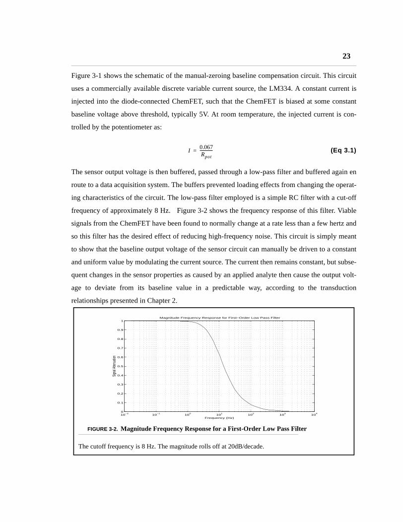
frequency of approximately 8 Hz. Figure 3-2 shows the frequency response of this filter. Viable
signals from the ChemFET have been found to normally change at a rate less than a few hertz and
so this filter has the desired effect of reducing high-frequency noise. This circuit is simply meant
to show that the baseline output voltage of the sensor circuit can manually be driven to a constant
and uniform value by modulating the current source. The current then remains constant, but subse-
quent changes in the sensor properties as caused by an applied analyte then cause the output volt-
age to deviate from its baseline value in a predictable way, according to the transduction
relationships presented in Chapter 2.
I0.067Rpot-------------=
FIGURE 3-2. Magnitude Frequency Response for a First-Order Low Pass Filter
The cutoff frequency is 8 Hz. The magnitude rolls off at 20dB/decade.
10−2
10−1
100
101
102
103
104
0
0.1
0.2
0.3
0.4
0.5
0.6
0.7
0.8
0.9
1Magnitude Frequency Response for First−Order Low Pass Filter
Frequency (Hz)
Signa
l Atte
nuati
on

24 Circuit Design and Experimental Results
Because the ChemFET requires high currents, typically in the mA range to operate, self-heating is
a possible effect that can change the current regulation properties of the LM334. A more accurate
formula for the output current including temperature effects is:
(Eq 3.2)
To alleviate performance problems caused by temperature variations, an additional heat sink has
been placed on the LM334. However, the settling effects of the ChemFET dominates those of the
LM334. Due to fabrication issues associated with the ChemFET, ChemFETs should be allowed to
settle thermally for a period of several minutes. The LM334 will settle into its thermal environ-
ment long before the ChemFET. Because the output current required for ChemFETs is several
milliamps, the final output current of the LM334 may differ from that expected due to temperature
effects, however, the most important consideration is that the output current be constant regardless
of the actual value. The LM334 does produce a constant output current, even under thermal load-
ing conditions.
SECTION 3.3 VARIABLE-RESISTOR AUTO-ZEROING BASELINE COMPENSATOR
Having demonstrated the usefulness of baseline compensation, the next step is to automate the
compensation. This auto-zeroing eliminates the effects of sensor manufacturing variability and
drift through automatic compensations, thus allowing the user to concentrate on interpreting sen-
sor outputs rather than extracting the signal itself. In the case of chemiresistors, many ways to
extract the resistance signal from each sensor are possible. The simplest circuit possible is the volt-
age-divider, in which a voltage supply can be placed across two resistors. The output voltage is
tapped at the joining of the two resistors, where one of the resistors is the chemiresistive sensor.
However, voltage dividers suffer from many drawbacks. For the purposes of sensing applications,
sensitivity may be defined as the amount a measurement circuit output changes for a fixed change
in the sensor state. Voltage dividers have a highly non-linear sensitivity, and especially poor sensi-
tivity to small changes in sensor state. In the case of chemical sensors, small changes in sensor
states can be very important. The voltage divider therefore, despite its simplicity, is not a desirable
choice for a compensation circuit.
I227 10
6–⋅Rpot
------------------------ T °K( )⋅=
25
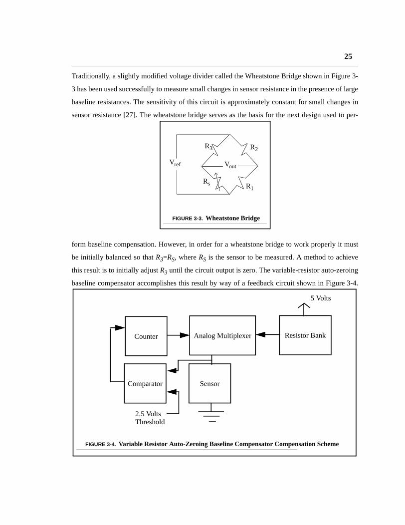
Traditionally, a slightly modified voltage divider called the Wheatstone Bridge shown in Figure 3-
3 has been used successfully to measure small changes in sensor resistance in the presence of large
baseline resistances. The sensitivity of this circuit is approximately constant for small changes in
sensor resistance [27]. The wheatstone bridge serves as the basis for the next design used to per-
form baseline compensation. However, in order for a wheatstone bridge to work properly it must
be initially balanced so that R3=RS, where RS is the sensor to be measured. A method to achieve
this result is to initially adjust R3 until the circuit output is zero. The variable-resistor auto-zeroing
baseline compensator accomplishes this result by way of a feedback circuit shown in Figure 3-4.
FIGURE 3-3. Wheatstone Bridge
Vout
Rs
R3 R2
R1
Vref
FIGURE 3-4. Variable Resistor Auto-Zeroing Baseline Compensator Compensation Scheme
Counter Analog Multiplexer Resistor Bank
Comparator Sensor
2.5 Volts
5 Volts
Threshold

26 Circuit Design and Experimental Results
The feedback circuit uses two stages. Stage one performs rough compensation by matching R3 to
within 10k of RS. The second stage then matchs R3 to within 1k of RS. Each stage is enabled
when a counter is reset and begins to count up. The output of the counter is connected to an analog
multiplexer. The analog multiplexer is connected to series of resistors of different values, as well
as to the sensor resistance. A comparator is used to determine when each compensation stage has
finished.
This method of resistor matching to achieve compensation is highly approximate at best. The ini-
tial range of possible baseline resistances is quite large, and so in order to keep the resistor bank
from growing to an unreasonable size, a certain amount of resistance matching error must be
accepted, hence the sensor is only matched to the nearest k , and only a limited range of baseline
resistances are able to be compensated. In order to provide a numerical comparison between the
accuracy of this circuit and of those to follow, measurements have been taken to determine com-
pensation accuracy. Table 3-1 below summarizes the results. The average compensation error is
45mV.
While the compensation error limits for this circuit are small to provide accurate baseline compen-
sation over a limited range, and certainly comparable to the capabilities of other types of compen-
sation circuits, other drawbacks prevent its widespread use for chemical sensor signal processing.
First of all, this circuit is not capable of being used with non-chemiresistive sensors such as Chem-
FETs because it is a resistance matching scheme. Although a resistor attached between the Chem-
FET source and Vdd could be used as a current source to bias the ChemFET, as the ChemFET
Table 3-1 - Measured vs. Ideal Baseline Outputs for Variable-Resistance Compensation
Baseline Resistance
Compensated Voltage
Ideal Output Voltage
Absolute Difference
20k Out of Range 0V Out of Range
50k 0.046 0V 46mV
70k 0.035 0V 35mV
110k 0.054 0V 54mV
200k Out of Range 0V Out of Range
Ω Ω
Ω
Ω
Ω
Ω
Ω
Ω
27
threshold voltage changes, the voltage across the resistor changes thus changing the bias current.
This type of current source is therefore not constant and serves only to complicate the process of
signal extraction.
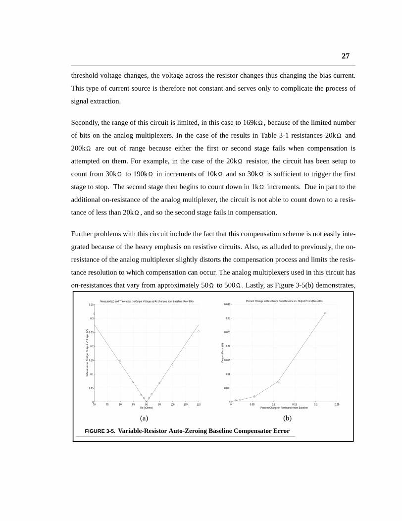
Secondly, the range of this circuit is limited, in this case to 169k , because of the limited number
of bits on the analog multiplexers. In the case of the results in Table 3-1 resistances 20k and
200k are out of range because either the first or second stage fails when compensation is
attempted on them. For example, in the case of the 20k resistor, the circuit has been setup to
count from 30k to 190k in increments of 10k and so 30k is sufficient to trigger the first
stage to stop. The second stage then begins to count down in 1k increments. Due in part to the
additional on-resistance of the analog multiplexer, the circuit is not able to count down to a resis-
tance of less than 20k , and so the second stage fails in compensation.
Further problems with this circuit include the fact that this compensation scheme is not easily inte-
grated because of the heavy emphasis on resistive circuits. Also, as alluded to previously, the on-
resistance of the analog multiplexer slightly distorts the compensation process and limits the resis-
tance resolution to which compensation can occur. The analog multiplexers used in this circuit has
on-resistances that vary from approximately 50 to 500 . Lastly, as Figure 3-5(b) demonstrates,
Ω
Ω
Ω
Ω
Ω Ω Ω Ω
Ω
Ω
Ω Ω
FIGURE 3-5. Variable-Resistor Auto-Zeroing Baseline Compensator Error
70 75 80 85 90 95 100 105 1100
0.05
0.1
0.15
0.2
0.25
0.3
0.35Measured (o) and Theoretical (−) Output Voltage as Rx changes from Baseline (Rxo=90k)
Rx (kOhms)
Wh
ea
tsto
ne
Brid
ge
Ou
tpu
t V
olta
ge
(V
)
0 0.05 0.1 0.15 0.2 0.250
0.005
0.01
0.015
0.02
0.025
0.03
0.035Percent Change in Resistance from Baseline vs. Output Error (Rxo=90k)
Percent Change in Resistance from Baseline
Ou
tpu
t E
rro
r (V
)
(a) (b)
28 Circuit Design and Experimental Results
as the resistance changes from the baseline value, the absolute error in the circuit grows exponen-
tially due to loading effects thus vastly limiting the resolution to which analytes can be measured.
SECTION 3.4 DISCRETE VARIABLE-CURRENT AUTO-ZEROING BASELINE COMPENSATOR
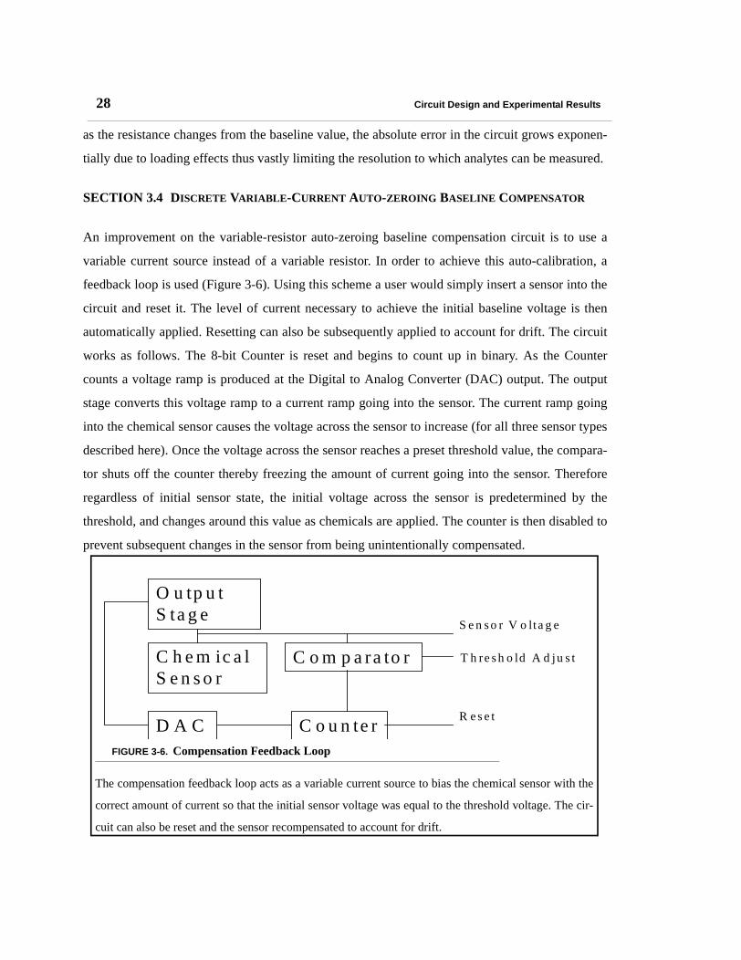
An improvement on the variable-resistor auto-zeroing baseline compensation circuit is to use a
variable current source instead of a variable resistor. In order to achieve this auto-calibration, a
feedback loop is used (Figure 3-6). Using this scheme a user would simply insert a sensor into the
circuit and reset it. The level of current necessary to achieve the initial baseline voltage is then
automatically applied. Resetting can also be subsequently applied to account for drift. The circuit
works as follows. The 8-bit Counter is reset and begins to count up in binary. As the Counter
counts a voltage ramp is produced at the Digital to Analog Converter (DAC) output. The output
stage converts this voltage ramp to a current ramp going into the sensor. The current ramp going
into the chemical sensor causes the voltage across the sensor to increase (for all three sensor types
described here). Once the voltage across the sensor reaches a preset threshold value, the compara-
tor shuts off the counter thereby freezing the amount of current going into the sensor. Therefore
regardless of initial sensor state, the initial voltage across the sensor is predetermined by the
threshold, and changes around this value as chemicals are applied. The counter is then disabled to
prevent subsequent changes in the sensor from being unintentionally compensated.
FIGURE 3-6. Compensation Feedback Loop
The compensation feedback loop acts as a variable current source to bias the chemical sensor with the
correct amount of current so that the initial sensor voltage was equal to the threshold voltage. The cir-
cuit can also be reset and the sensor recompensated to account for drift.
O u tp u t S ta g e
C h e m ic a l S e n s o r
C o u n te rD A C
C o m p a ra to r
S e n s o r V o lta g e
R e s e t
T h re s h o ld A d ju s t

29
All components of this compensation circuit are straight-forward except for perhaps the output
stage. The circuit for the output stage is shown in Figure 3-7. Figure 3-8 demonstrates the entire
compensation process. The circuit is a modified instrumentation amplifier acting as a voltage-con-
trolled current source. Op-amp LM324_4 is bootstrapped to require that the voltage across Rx be
equal to the applied voltage from the DAC. Ideally no charge flows into an op-amp input so the
voltage across Rx will directly produce a current which was injected entirely into the sensor, pro-
ducing the sensor output voltage. Therefore,
(Eq 3.3)
(Eq 3.4)
for the chemiresistor and ChemFET respectively. Resistors of size 20k are used in the output
stage because their resistance is large enough to limit power consumption, but not so large that
their impedances begins to produce significant non-idealities in the op-amps.
FIGURE 3-7. Output Stage Schematic
The output stage acts as a voltage-controlled current source to bias the chemical sensor at a current
that forces the baseline sensor voltage to a predetermined threshold.
From DAC
Vout
Comparator out to counter enable
R1
R2
R3 R4
Rx
Vthreshold
LM324_1
LM324_2
LM324_3 LM324_4 LM324_5
20k
20k
20k
20k 20kSensor
-
-
+
+
-
+
-
+
-
+
VSensor
RSensorVDAC
Rx--------------------------------=
VSensor Vt
2VDACRx
k' W L⁄( )-----------------------+=
Ω

30 Circuit Design and Experimental Results
For the case of chemiresistors, the following formulas are useful in determining what value of
to use relative to the expected range of resistances of the chemiresistors (Rmin to Rmax). The
smaller the range the more accurate the compensation.
(Eq 3.5)
(Eq 3.6)
The variable-current discrete auto-zeroing compensation circuit consists of four separate printed
circuit boards. Two of the circuit boards contain the auto-zeroing baseline compensation circuits
for six sensors and one of the boards contains the sensors. The final board contains digital process-
ing electronics, power inputs, and an optional interface to a data acquisition system made to be
used with Lab View.
Empirical results have been collected by placing the compensation circuit and chemical sensors in
an enclosed chamber approximately 1 meter in length on each side. The types of sensors used
include two types of composite-film polymer sensors (provided by Nathan Lewis at CalTech) and
FIGURE 3-8. Composite-Film Polymer Chemiresistor During Compensation
is set to 5k , thereby causing to go from 0 to 1mA in 3.9 A steps. The initial resistance of the
composite-film polymer chemiresistor is 30k . When the sensor voltage output exceeds the threshold
voltage of 2V at 2.106V, the comparator changes states, shutting off the current ramp. A more precise
compensation could be obtained by using a larger value of , but this action would also limit the range
of baseline resistances that could be compensated as demonstrated in equation 3.5.
Rx Ω Iset µ
Ω
Rx
0 5 10 15 20 25 30 35 40 450
0.5
1
1.5
2
2.5
3
3.5
4
4.5
5
Data Points
Out
put V
olta
ge
Compensation of a Carbon−Black Insulating−Polymer Chemical Sensor
Compensated Voltage OutputThreshold VoltageComparator Output
Rx
Rmin 0.4Rx=
Rmax 20Rx=
31
three types of tin-oxide sensors (purchased from Figaro Engineering). A small container is placed
into the test chamber containing the analyte of choice. The container is separated from the cham-
ber by a solenoid valve. Before any analyte is applied to the chamber, the chamber is purged using
compressed air. All sensors are allowed to stabilize prior to introduction of an analyte. The sole-
noid valves are opened for 30 minutes to allow the analyte to diffuse into the chamber, then closed
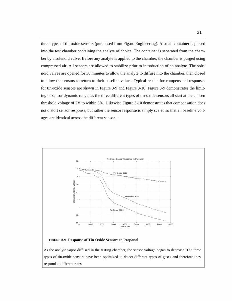
to allow the sensors to return to their baseline values. Typical results for compensated responses
for tin-oxide sensors are shown in Figure 3-9 and Figure 3-10. Figure 3-9 demonstrates the limit-
ing of sensor dynamic range, as the three different types of tin-oxide sensors all start at the chosen
threshold voltage of 2V to within 3%. Likewise Figure 3-10 demonstrates that compensation does
not distort sensor response, but rather the sensor response is simply scaled so that all baseline volt-
ages are identical across the different sensors.
FIGURE 3-9. Response of Tin-Oxide Sensors to Propanol
As the analyte vapor diffused in the testing chamber, the sensor voltage began to decrease. The three
types of tin-oxide sensors have been optimized to detect different types of gases and therefore they
respond at different rates.
0 1000 2000 3000 4000 5000 6000 7000 80000.6
0.8
1
1.2
1.4
1.6
1.8
2
2.2
Data Points
Com
pens
ated
Out
put V
olta
ge
Tin Oxide Sensor Response to Propanol
Tin Oxide 2610
Tin Oxide 2620
Tin Oxide 2600

32 Circuit Design and Experimental Results
In Table 3-2, measurements were taken of the initial baseline voltage of composite polymer sen-
sors after they have been compensated. The value for used for these measurements is 20k .
Ideally the compensated voltage should equal the threshold voltage of 2V. In general, as baseline
resistance increases and becomes much greater than , the compensation accuracy decreases.
Although the current ramps up in constant intervals, the size of the voltage steps at the sensor out-
put (as determined by Ohm’s law) is larger for greater baseline resistances..
Table 3-2 - Measured vs. Ideal Baseline Compensated Sensor Outputs
Baseline Resistance
Compensated Voltage
Threshold Voltage
Percent Difference
20k 2.016V 2V 0.8%
50k 2.012V 2V 0.6%
70k 2.060V 2V 3.0%
110k 2.051V 2V 2.55%
200k 2.153V 2V 7.65%
FIGURE 3-10. Normalized Compensated and Uncompensated Response of Tin Oxide Sensors
The above curves are normalized by setting the maximum value in each to 1. Because this compensa-
tion scheme does not change the shape of the response, only the scaling, the compensated and uncom-
pensated curves should be nearly identical. The mean squared error between the two curves is 0.0548.
The slight discrepancy was due to random fluctuations in gas delivery between sensors as the two sen-
sors were seperated by a distance of several inches and the detection of analyte diffusion into the cham-
ber has been observed to be highly depenent on sensor position within the chamber.
0 1000 2000 3000 4000 5000 6000 7000 80000.3
0.4
0.5
0.6
0.7
0.8
0.9
1
Data Points
Norm
alize
d Outp
ut Va
lues
Compensated vs. Uncompensated Response for Tin Oxide Sensors
Uncompensated Output of Tin Oxide 2600
Compensated Output of Tin Oxide 2600
Rx Ω
Rx
Ω
Ω
Ω
Ω
Ω

33
As shown in Figure 3-11, a sensor can be periodically recompensated to account for drift in order
to maintain a near constant baseline output. Drift rates noted in our experiments and in experi-
ments done by other labs have typically shown drift to be limited to about 5% per month, unless
the sensor becomes poisoned in which case drift can be much higher to the point that the sensor
lacks sensitivity and must then be discarded. Under normal circumstances, drift has been shown to
not significantly affect sensor sensitivity and when compensated, drift does not effect sensor accu-
racy [9]. The drift compensation performed in Figure 3-11 demonstrates the value of drift compen-
sation in reducing dynamic range. Drift can be viewed as low-frequency noise, a distortion in the
sensor signal that changes very slowly relative to the actual changes that represent analyte concen-
trations. Drift compensation here effectively acted as an additional type of noise filter that
removes the low-frequency noise, thus reducing the dynamic range in this typical case by over 10
mV. 10 mV can represent a large change in sensor state when the sensor is responding to an ana-
lyte. Without this drift compensation, drift limits the resolution of the sensor output voltage to 10
mV, thus decreasing accuracy even though baseline compensation reduced the dynamic range as a
whole. Also, if the sensor had been allowed to continue drifting, dynamic range can continue to
FIGURE 3-11. Drift Compensation in a Composite-Film Polymer Chemiresistors
After compensation, the sensor voltage is approximately 2.015 V. Air saturated with propanol is
exposed to the sensors for under a second. The sensors exhibit an increase in resistance due to the ana-
lyte and then a decrease in resistance as they returned to a new baseline value. At approximately data
point 300, the compensation circuit is reset to establish a new baseline voltage for the sensors, at which
time they both return to approximately 2.015V.
0 50 100 150 200 250 3002
2.005
2.01
2.015
2.02
2.025
2.03
Data Points
Comp
ensa
ted V
oltag
e Outp
ut Va
lues
Drift in Carbon−Black Insulating−Polymer Chemical Sensors
PCL1PCL2
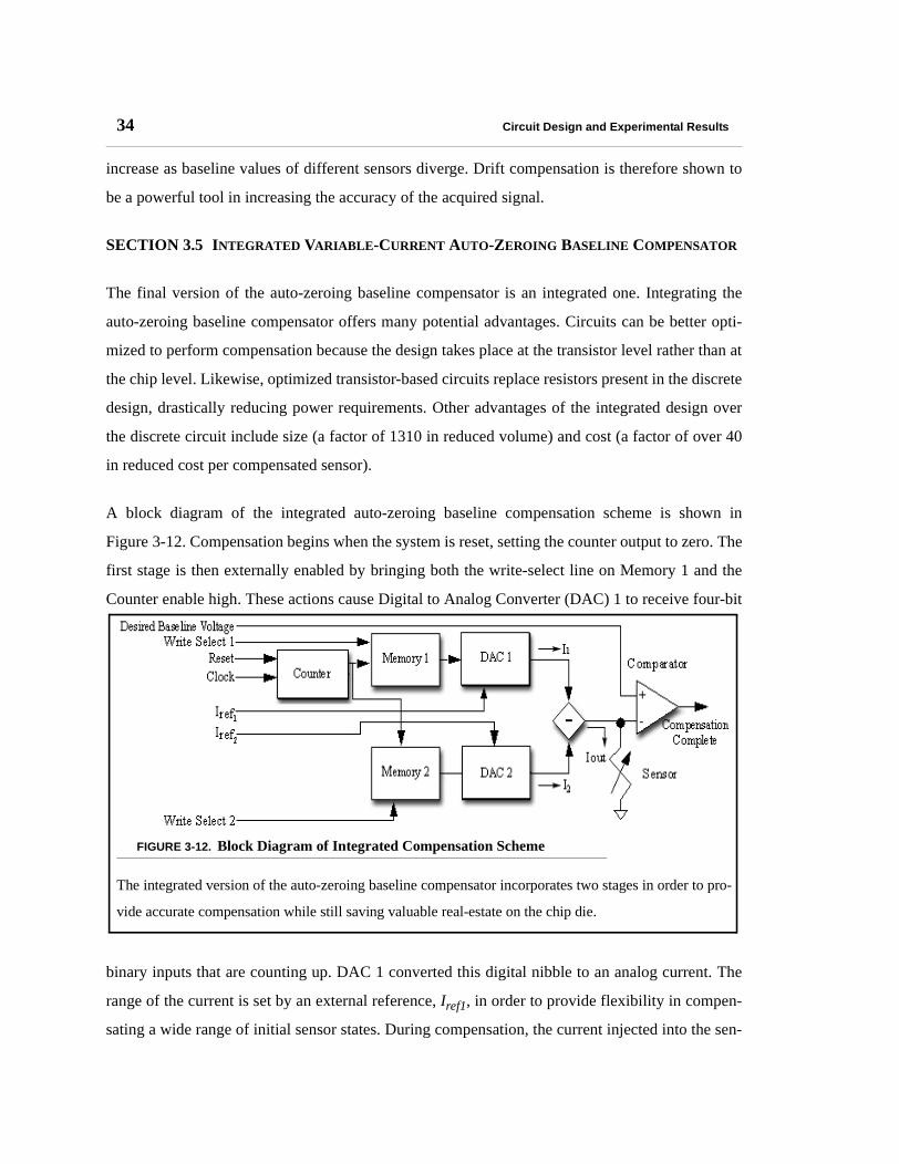
34 Circuit Design and Experimental Results
increase as baseline values of different sensors diverge. Drift compensation is therefore shown to
be a powerful tool in increasing the accuracy of the acquired signal.
SECTION 3.5 INTEGRATED VARIABLE-CURRENT AUTO-ZEROING BASELINE COMPENSATOR
The final version of the auto-zeroing baseline compensator is an integrated one. Integrating the
auto-zeroing baseline compensator offers many potential advantages. Circuits can be better opti-
mized to perform compensation because the design takes place at the transistor level rather than at
the chip level. Likewise, optimized transistor-based circuits replace resistors present in the discrete
design, drastically reducing power requirements. Other advantages of the integrated design over
the discrete circuit include size (a factor of 1310 in reduced volume) and cost (a factor of over 40
in reduced cost per compensated sensor).
A block diagram of the integrated auto-zeroing baseline compensation scheme is shown in
Figure 3-12. Compensation begins when the system is reset, setting the counter output to zero. The
first stage is then externally enabled by bringing both the write-select line on Memory 1 and the
Counter enable high. These actions cause Digital to Analog Converter (DAC) 1 to receive four-bit
binary inputs that are counting up. DAC 1 converted this digital nibble to an analog current. The
range of the current is set by an external reference, Iref1, in order to provide flexibility in compen-
sating a wide range of initial sensor states. During compensation, the current injected into the sen-
FIGURE 3-12. Block Diagram of Integrated Compensation Scheme
The integrated version of the auto-zeroing baseline compensator incorporates two stages in order to pro-
vide accurate compensation while still saving valuable real-estate on the chip die.
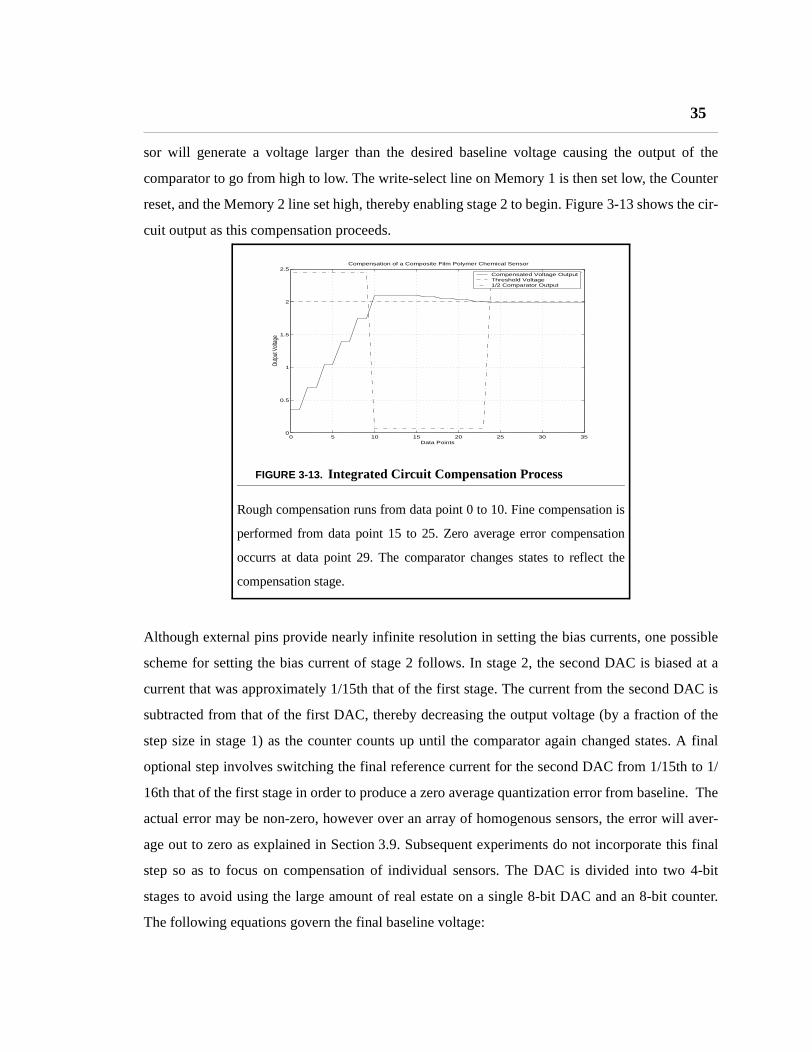
35
sor will generate a voltage larger than the desired baseline voltage causing the output of the
comparator to go from high to low. The write-select line on Memory 1 is then set low, the Counter
reset, and the Memory 2 line set high, thereby enabling stage 2 to begin. Figure 3-13 shows the cir-
cuit output as this compensation proceeds.
Although external pins provide nearly infinite resolution in setting the bias currents, one possible
scheme for setting the bias current of stage 2 follows. In stage 2, the second DAC is biased at a
current that was approximately 1/15th that of the first stage. The current from the second DAC is
subtracted from that of the first DAC, thereby decreasing the output voltage (by a fraction of the
step size in stage 1) as the counter counts up until the comparator again changed states. A final
optional step involves switching the final reference current for the second DAC from 1/15th to 1/
16th that of the first stage in order to produce a zero average quantization error from baseline. The
actual error may be non-zero, however over an array of homogenous sensors, the error will aver-
age out to zero as explained in Section 3.9. Subsequent experiments do not incorporate this final
step so as to focus on compensation of individual sensors. The DAC is divided into two 4-bit
stages to avoid using the large amount of real estate on a single 8-bit DAC and an 8-bit counter.
The following equations govern the final baseline voltage:
FIGURE 3-13. Integrated Circuit Compensation Process
Rough compensation runs from data point 0 to 10. Fine compensation is
performed from data point 15 to 25. Zero average error compensation
occurrs at data point 29. The comparator changes states to reflect the
compensation stage.
0 5 10 15 20 25 30 350
0.5
1
1.5
2
2.5
Data Points
Outp
ut V
oltag
e
Compensation of a Composite Film Polymer Chemical Sensor
Compensated Voltage OutputThreshold Voltage1/2 Comparator Output
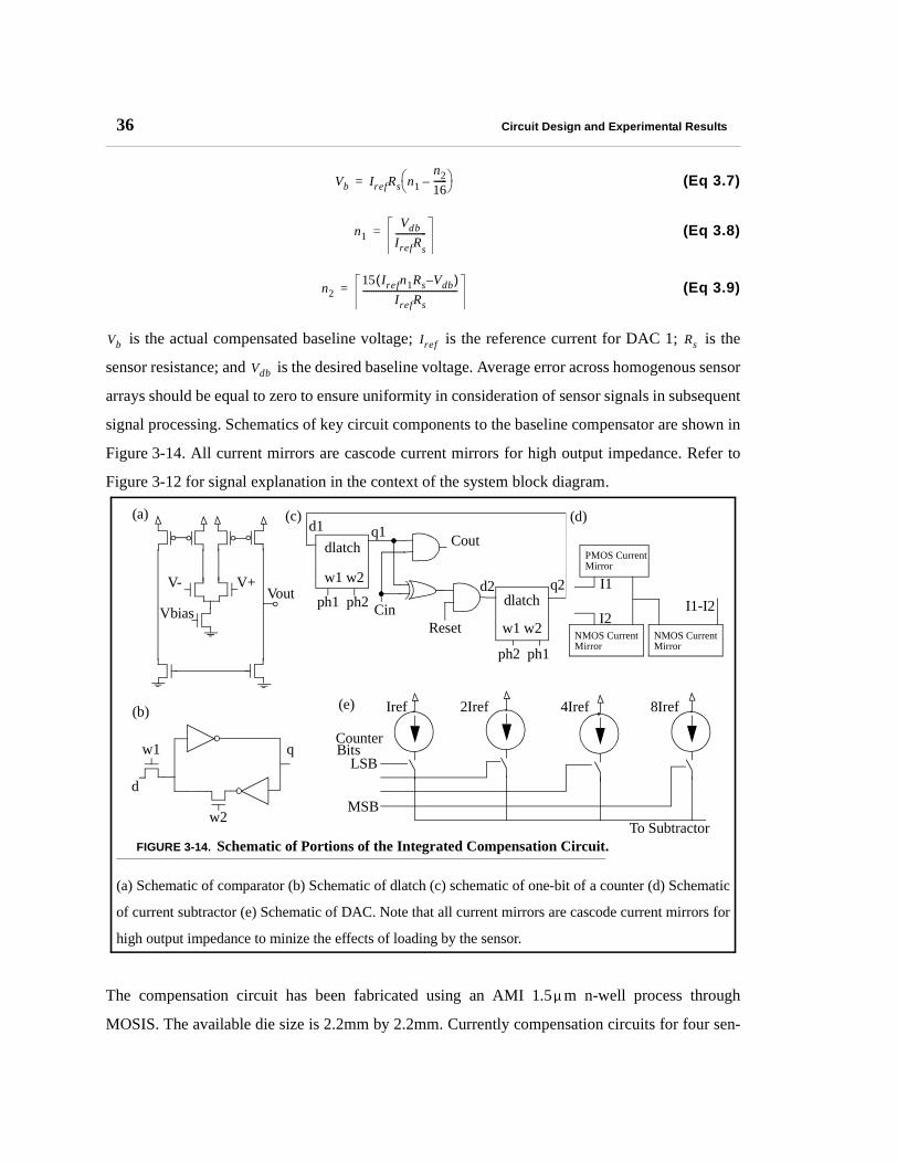
36 Circuit Design and Experimental Results
(Eq 3.7)
(Eq 3.8)
(Eq 3.9)
is the actual compensated baseline voltage; is the reference current for DAC 1; is the
sensor resistance; and is the desired baseline voltage. Average error across homogenous sensor
arrays should be equal to zero to ensure uniformity in consideration of sensor signals in subsequent
signal processing. Schematics of key circuit components to the baseline compensator are shown in
Figure 3-14. All current mirrors are cascode current mirrors for high output impedance. Refer to
Figure 3-12 for signal explanation in the context of the system block diagram.
The compensation circuit has been fabricated using an AMI 1.5 m n-well process through
MOSIS. The available die size is 2.2mm by 2.2mm. Currently compensation circuits for four sen-
Vb IrefRs n1
n2
16------–
=
n1Vdb
IrefRs
--------------=
n215 Irefn1Rs Vdb–( )
IrefRs-------------------------------------------=
Vb Iref Rs
Vdb
FIGURE 3-14. Schematic of Portions of the Integrated Compensation Circuit.
(a) Schematic of comparator (b) Schematic of dlatch (c) schematic of one-bit of a counter (d) Schematic
of current subtractor (e) Schematic of DAC. Note that all current mirrors are cascode current mirrors for
high output impedance to minize the effects of loading by the sensor.
V- V+
VbiasVout
(a) (c)
q
d
w1
w2
(b)
Cout
CinReset
d1 q1
q2d2w1 w2
w1 w2
ph1 ph2
ph2 ph1
dlatch
dlatch
PMOS CurrentMirror
Mirror MirrorNMOS Current NMOS Current
I1
I2I1-I2
(d)
CounterBits
LSB
MSB
Iref 2Iref 4Iref 8Iref
To Subtractor
(e)
µ
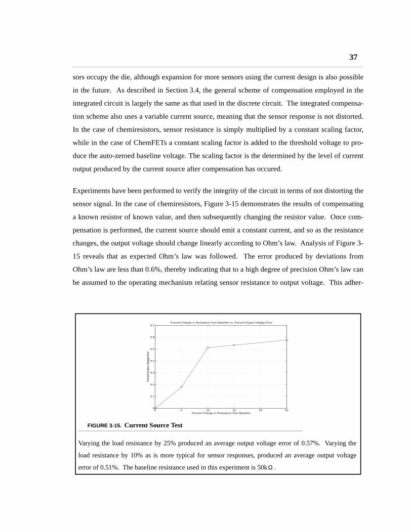
37
sors occupy the die, although expansion for more sensors using the current design is also possible
in the future. As described in Section 3.4, the general scheme of compensation employed in the
integrated circuit is largely the same as that used in the discrete circuit. The integrated compensa-
tion scheme also uses a variable current source, meaning that the sensor response is not distorted.
In the case of chemiresistors, sensor resistance is simply multiplied by a constant scaling factor,
while in the case of ChemFETs a constant scaling factor is added to the threshold voltage to pro-
duce the auto-zeroed baseline voltage. The scaling factor is the determined by the level of current
output produced by the current source after compensation has occured.
Experiments have been performed to verify the integrity of the circuit in terms of not distorting the
sensor signal. In the case of chemiresistors, Figure 3-15 demonstrates the results of compensating
a known resistor of known value, and then subsequently changing the resistor value. Once com-
pensation is performed, the current source should emit a constant current, and so as the resistance
changes, the output voltage should change linearly according to Ohm’s law. Analysis of Figure 3-
15 reveals that as expected Ohm’s law was followed. The error produced by deviations from
Ohm’s law are less than 0.6%, thereby indicating that to a high degree of precision Ohm’s law can
be assumed to the operating mechanism relating sensor resistance to output voltage. This adher-
FIGURE 3-15. Current Source Test
Varying the load resistance by 25% produced an average output voltage error of 0.57%. Varying the
load resistance by 10% as is more typical for sensor responses, produced an average output voltage
error of 0.51%. The baseline resistance used in this experiment is 50k .Ω
0 5 10 15 20 250
0.1
0.2
0.3
0.4
0.5
0.6
0.7Percent Change in Resistance from Baseline vs. Percent Output Voltage Error
Percent Change in Resistance from Baseline
Perc
ent O
utpu
t Vol
tage
Erro
r
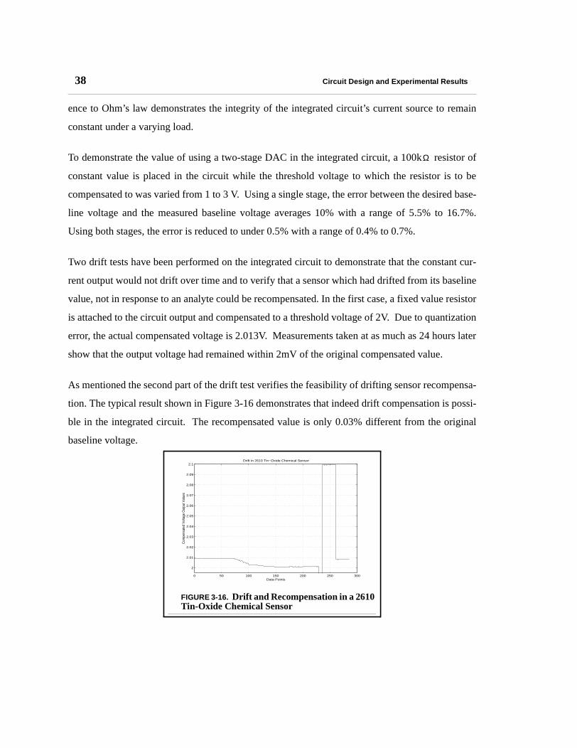
38 Circuit Design and Experimental Results
ence to Ohm’s law demonstrates the integrity of the integrated circuit’s current source to remain
constant under a varying load.
To demonstrate the value of using a two-stage DAC in the integrated circuit, a 100k resistor of
constant value is placed in the circuit while the threshold voltage to which the resistor is to be
compensated to was varied from 1 to 3 V. Using a single stage, the error between the desired base-
line voltage and the measured baseline voltage averages 10% with a range of 5.5% to 16.7%.
Using both stages, the error is reduced to under 0.5% with a range of 0.4% to 0.7%.
Two drift tests have been performed on the integrated circuit to demonstrate that the constant cur-
rent output would not drift over time and to verify that a sensor which had drifted from its baseline
value, not in response to an analyte could be recompensated. In the first case, a fixed value resistor
is attached to the circuit output and compensated to a threshold voltage of 2V. Due to quantization
error, the actual compensated voltage is 2.013V. Measurements taken at as much as 24 hours later
show that the output voltage had remained within 2mV of the original compensated value.
As mentioned the second part of the drift test verifies the feasibility of drifting sensor recompensa-
tion. The typical result shown in Figure 3-16 demonstrates that indeed drift compensation is possi-
ble in the integrated circuit. The recompensated value is only 0.03% different from the original
baseline voltage.
Ω
FIGURE 3-16. Drift and Recompensation in a 2610 Tin-Oxide Chemical Sensor
0 50 100 150 200 250 300
2
2.01
2.02
2.03
2.04
2.05
2.06
2.07
2.08
2.09
2.1
Data Points
Com
pens
ated
Vol
tage
Out
put V
alue
s
Drift in 2610 Tin−Oxide Chemical Sensor
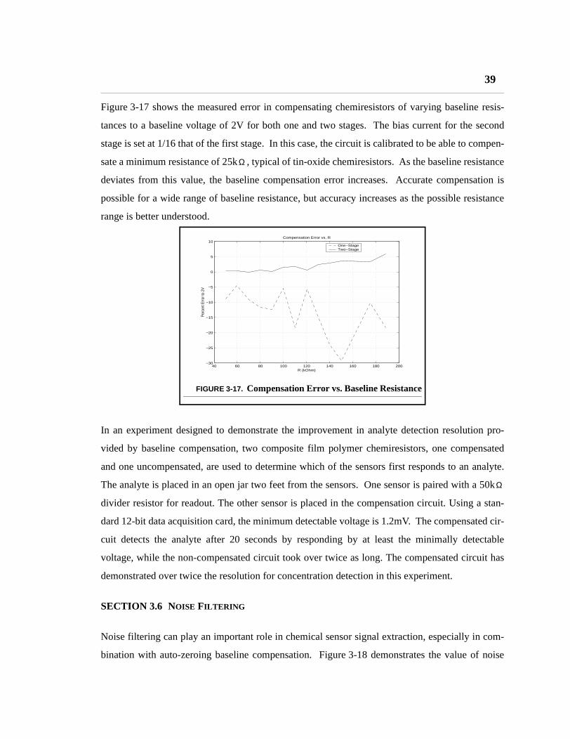
39
Figure 3-17 shows the measured error in compensating chemiresistors of varying baseline resis-
tances to a baseline voltage of 2V for both one and two stages. The bias current for the second
stage is set at 1/16 that of the first stage. In this case, the circuit is calibrated to be able to compen-
sate a minimum resistance of 25k , typical of tin-oxide chemiresistors. As the baseline resistance
deviates from this value, the baseline compensation error increases. Accurate compensation is
possible for a wide range of baseline resistance, but accuracy increases as the possible resistance
range is better understood.
In an experiment designed to demonstrate the improvement in analyte detection resolution pro-
vided by baseline compensation, two composite film polymer chemiresistors, one compensated
and one uncompensated, are used to determine which of the sensors first responds to an analyte.
The analyte is placed in an open jar two feet from the sensors. One sensor is paired with a 50k
divider resistor for readout. The other sensor is placed in the compensation circuit. Using a stan-
dard 12-bit data acquisition card, the minimum detectable voltage is 1.2mV. The compensated cir-
cuit detects the analyte after 20 seconds by responding by at least the minimally detectable
voltage, while the non-compensated circuit took over twice as long. The compensated circuit has
demonstrated over twice the resolution for concentration detection in this experiment.
SECTION 3.6 NOISE FILTERING
Noise filtering can play an important role in chemical sensor signal extraction, especially in com-
bination with auto-zeroing baseline compensation. Figure 3-18 demonstrates the value of noise
Ω
FIGURE 3-17. Compensation Error vs. Baseline Resistance
40 60 80 100 120 140 160 180 200−30
−25
−20
−15
−10
−5
0
5
10Compensation Error vs. R
R (kOhm)
Perc
ent E
rror t
o 2V
One−StageTwo−Stage
Ω
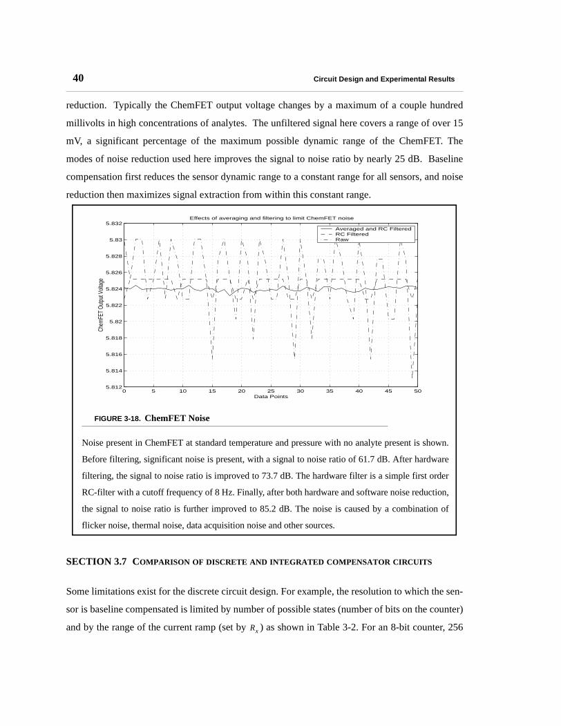
40 Circuit Design and Experimental Results
reduction. Typically the ChemFET output voltage changes by a maximum of a couple hundred
millivolts in high concentrations of analytes. The unfiltered signal here covers a range of over 15
mV, a significant percentage of the maximum possible dynamic range of the ChemFET. The
modes of noise reduction used here improves the signal to noise ratio by nearly 25 dB. Baseline
compensation first reduces the sensor dynamic range to a constant range for all sensors, and noise
reduction then maximizes signal extraction from within this constant range.
SECTION 3.7 COMPARISON OF DISCRETE AND INTEGRATED COMPENSATOR CIRCUITS
Some limitations exist for the discrete circuit design. For example, the resolution to which the sen-
sor is baseline compensated is limited by number of possible states (number of bits on the counter)
and by the range of the current ramp (set by ) as shown in Table 3-2. For an 8-bit counter, 256
FIGURE 3-18. ChemFET Noise
Noise present in ChemFET at standard temperature and pressure with no analyte present is shown.
Before filtering, significant noise is present, with a signal to noise ratio of 61.7 dB. After hardware
filtering, the signal to noise ratio is improved to 73.7 dB. The hardware filter is a simple first order
RC-filter with a cutoff frequency of 8 Hz. Finally, after both hardware and software noise reduction,
the signal to noise ratio is further improved to 85.2 dB. The noise is caused by a combination of
flicker noise, thermal noise, data acquisition noise and other sources.
0 5 10 15 20 25 30 35 40 45 505.812
5.814
5.816
5.818
5.82
5.822
5.824
5.826
5.828
5.83
5.832
Data Points
Chem
FET
Outp
ut V
oltag
e
Effects of averaging and filtering to limit ChemFET noise
Averaged and RC FilteredRC FilteredRaw
Rx

41
possible states are evenly divided within the current ramp range. Increasing the range of the cur-
rent ramp enables the compensation of a wider range of initial sensor states, but at lower resolu-
tion. In the case of the discrete circuit, baseline compensation is also further diminished by non-
idealities in the op-amps used throughout the circuit, especially in the case of the composite-film
polymer chemiresistors which typically have a high initial impedance relative to the other sensor
types. Initial output impedances of the composite-film polymer chemiresistors can easily be on the
order of several hundred k . Another issue with the op-amp is the finite input bias current. The
combined bias current that leaks into the various op-amps at the sensor node should be approxi-
mately 1 A and is variable with temperature. In the case of the composite-film polymer chemire-
sistors, the bias current passed through the sensor by the compensation circuit is generally below
100 A. Because the leakage current is a significant fraction of the compensation current for this
sensor type, significant degradation in the predicted circuit response is possible. In addition, the
present layout of the circuit requiring the sensor to be connected from various op-amp inputs to
ground may also degrade the input impedance of the op-amps to which it is connected, further
increasing bias currents and limiting the ability of the voltage followers to correctly follow their
input voltages. However, Table 3-2 indicates that even taking into account the various non-ideali-
ties of the op-amps, the circuit still performed compensation to a high degree of accuracy.
The integrated circuit allows many design simplifications to take place that further optimize the
circuit for its intended purpose beyond what is possible with discrete chips. Many of the problems
associated with the op-amp non-idealities disappear as a different method is used to generate the
current ramp not involving op-amps. Compensation errors in the integrated version should then be
less than that for the discrete circuit. Table 3-3 demonstrates the measured results. As expected,
the average percent compensation error for the integrated circuit is nearly twice as small as that for
the discrete circuit (1.69% for the integrated circuit compared to 2.92% for the discrete circuit).
Table 3-3 - Discrete vs. Integrated Compensated Sensor Outputs
Baseline Resistance
Discrete Compensated Voltage
Integrated Compensated Voltage
Ideal Compensated Voltage
Percent Difference for Discrete
Percent Difference for Integrated
20k 2.016 1.995V 2V 0.8% 0.25%
50k 2.012 1.992V 2V 0.6% 0.4%
Ω
µ
µ
Ω
Ω
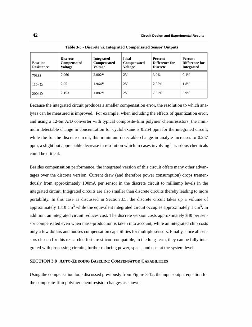
42 Circuit Design and Experimental Results
Because the integrated circuit produces a smaller compensation error, the resolution to which ana-
lytes can be measured is improved. For example, when including the effects of quantization error,
and using a 12-bit A/D converter with typical composite-film polymer chemiresistors, the mini-
mum detectable change in concentration for cyclohexane is 0.254 ppm for the integrated circuit,
while the for the discrete circuit, this minimum detectable change in analyte increases to 0.257
ppm, a slight but appreciable decrease in resolution which in cases involving hazardous chemicals
could be critical.
Besides compensation performance, the integrated version of this circuit offers many other advan-
tages over the discrete version. Current draw (and therefore power consumption) drops tremen-
dously from approximately 100mA per sensor in the discrete circuit to milliamp levels in the
integrated circuit. Integrated circuits are also smaller than discrete circuits thereby leading to more
portability. In this case as discussed in Section 3.5, the discrete circuit takes up a volume of
approximately 1310 cm3 while the equivalent integrated circuit occupies approximately 1 cm3. In
addition, an integrated circuit reduces cost. The discrete version costs approximately $40 per sen-
sor compensated even when mass-production is taken into account, while an integrated chip costs
only a few dollars and houses compensation capabilities for multiple sensors. Finally, since all sen-
sors chosen for this research effort are silicon-compatible, in the long-term, they can be fully inte-
grated with processing circuits, further reducing power, space, and cost at the system level.
SECTION 3.8 AUTO-ZEROING BASELINE COMPENSATOR CAPABILITIES
Using the compensation loop discussed previously from Figure 3-12, the input-output equation for
the composite-film polymer chemiresistor changes as shown:
70k 2.060 2.002V 2V 3.0% 0.1%
110k 2.051 1.964V 2V 2.55% 1.8%
200k 2.153 1.882V 2V 7.65% 5.9%
Table 3-3 - Discrete vs. Integrated Compensated Sensor Outputs
Baseline Resistance
Discrete Compensated Voltage
Integrated Compensated Voltage
Ideal Compensated Voltage
Percent Difference for Discrete
Percent Difference for Integrated
Ω
Ω
Ω

43
(Eq 3.10)
(Eq 3.11)
The compensated curve produces curves that have a constant sensitivity of which means that
slope of the compensated curve is unaffected by the baseline resistance. The reduction in input
dynamic range is demonstrated in Figure 3-19. Before compensation, the baseline resistance of the
poly(ethylene oxide) chemiresistors varies from 25k to 300k , as is typical due to manufactur-
ing variation. The sensor resistance is extracted as a voltage by injecting a constant current into the
resistor and measuring the resulting voltage across the resistor. For example, using a constant cur-
rent of 50 A and assuming that the sensor resistance could change by as much as 20%, the range
of output voltages possible is 1.25 V to 18 V. With a 12-bit analog-to-digital converter (ADC) the
minimum detectable change in either sensor is 81.8 (0.327% to 0.027%). When using compen-
Uncompensated∆RRo-------⇒ k C[ ] and ∆R R Ro R⇒– Ro Rok C[ ]+= = =
Compensated Vo⇒ ISetR ISetRo 1∆RRo-------+
ISetRo 1 k C[ ]+( ) Vb 1 k C[ ]+( )= = = =
Vbk
FIGURE 3-19. Simulation of Compensated and Uncompensated Sensor Response
(a) demonstrates the wide dynamic range needed to accommodate uncompensated sensor responses
over varying baseline voltages. (b) demonstrates the dramatic decrease in compensated dynamic range.
The values obtained in (b) for different baseline resistances are not exactly the same due to quantization
error.
0 500 1000 1500 2000 2500 3000 3500 4000 4500 50000
5
10
15Concentration versus Non−Compensated Output Voltage for Poly(ethylene oxide) Polymer Sensor
Out
put V
olta
ge (V
) Ro=25kOhmsRo=100kOhmsRo=250kOhms
0 500 1000 1500 2000 2500 3000 3500 4000 4500 50001.9
2
2.1
2.2
2.3
2.4
2.5Concentration versus Compensated Voltage Output for Poly(ethylene oxide) Polymer Sensor
Concentration of Cyclohexane (PPM)
Out
put V
olta
ge (V
)
(a)
(b)
Ω Ω
µ
Ω

44 Circuit Design and Experimental Results
sation, the minimum detectable change is 2.4 to 29.3 (0.010%), produced from a voltage range
of 2 to 2.4V. Without compensation, if it is desired to obtain similar resolution levels as that
obtained with compensation, an ADC with more than 17-bits would have to be used, greatly
increasing power, cost, and space requirements. Compensation provides up to a factor of 34
improvement in response (e.g. concentration) resolution for the same sensors and electronic pro-
cessing. Likewise, the minimum detectable change in concentration of cyclohexane for the non-
compensated circuit is 16.4 ppm, while for any of the compensated sensors, the minimum detect-
able concentration change is 0.5 ppm. The compensation circuit has greatly enhanced the detecting
capability of these chemical sensors by improving resolution and detection limit.
In a good sensor interface circuit design, it is the sensor noise that limits the minimum detectable
value and not the circuit into which the sensor is placed. As previously calculated, the thermal
noise associated with a composite-film polymer chemiresistor of 100k should be about 0.129
mV. With a 12-bit A/D converter, the minimum detectable voltage change is 0.098 mV. Thus, the
sensor noise limits the minimum detectable value, further verifying the validity of the design. The
previously discussed RC noise filter also aids in further reducing the noise from that expected from
calculations, ensuring that this minimum detectable signal is representative of the sensor response.
Similar analysis can be performed for the other two sensor types as well. For the tin-oxide sensors
the compensated input-output equation reduces to:
(Eq 3.12)
It can be seen here that at zero concentration of analyte, the output voltage becomes the baseline
voltage and that as the analyte concentration increases, the output voltage decreases towards zero.
As it was with the composite-film polymer sensor, the relationship between sensor resistance and
output voltage is preserved, but is scaled by a constant factor.
In the case of ChemFETs, the output dynamic range, and therefore the concentration detection res-
olution is also reduced as follows. By examining the governing transduction mechanism Equation
2.7, adjusting the bias current has the effect of adjusting the y-intercept of the response in such a
way that all chemFETs respond in a similar voltage range. If the bias voltages that act to set the
Ω Ω
Ω
Vo Vb
Iset
Iset Vbk C[ ] r+
-----------------------------------
=

45
reference currents are tabulated for known sensor technologies, it becomes possible to use this
compensation circuit in a plug and play manner to improve system concentration resolution and
linearity.
After compensation for the chemFET sensors, the compensated output voltage is:
(Eq 3.13)
The new constant x2 incorporates x1 and the term containing the drain current from Equation 2.7
as this has now been fixed as a constant. One boundary condition that exists is that as the concen-
tration approaches zero, the output voltage approaches the baseline voltage set by the compensator.
As with the chemiresistors, comparison of the modified input-output equation shows that the
nature of the relationship is the same with the addition of scaling factors. The response is not dis-
torted, and therefore becomes more useful for such applications as transient response analysis.
As sensor baseline states drift over time, typically 3% over the course of a week, sensors need only
to be recompensated to return them to the desired baseline output voltage. Because drift does not
significantly affect sensor sensitivity, this recompensation effectively eliminates the effects of low-
frequency drift. Other post-processing methods incorporated into the principal component analysis
can further reduce the effects of drift [28].
Other types of drift occur in response to changes in environmental parameters. For example, as
previously mentioned tin-oxide chemiresistors are highly sensitive to humidity in the environment.
To overcome this difficulty an on-board humidity sensor can monitor humidity, and indicate when
humidity changes by an appreciable amount, at which time sensors should be recompensated so
that any subsequent change in sensor state is due to the introduction of analytes and not environ-
mental changes. Further post-processing adjustments can be made digitally. For example, models
incorporating information on not only the instantaneous humidity, but how long sensors spend at
different humidity levels have been shown to produce more accurate results [29].
SECTION 3.9 IMPACT OF QUANTIZATION NOISE ON SYSTEM PERFORMANCE
Vo xo a C[ ]( ) x2+ln=
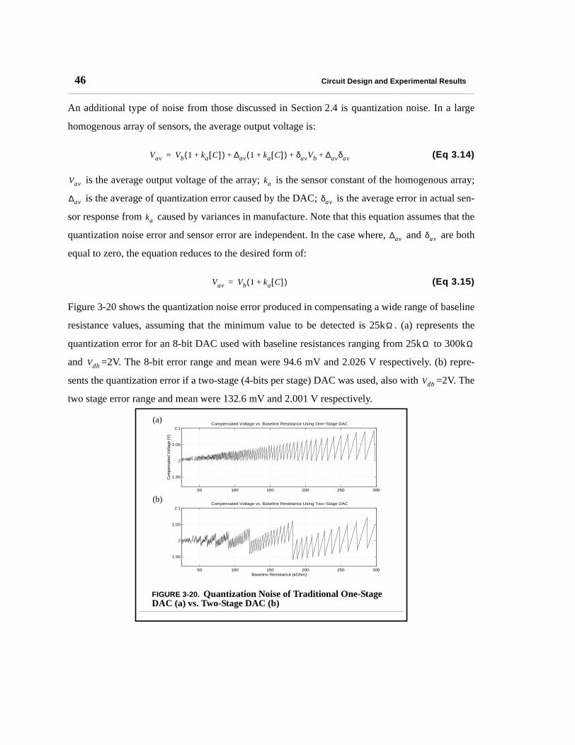
46 Circuit Design and Experimental Results
An additional type of noise from those discussed in Section 2.4 is quantization noise. In a large
homogenous array of sensors, the average output voltage is:
(Eq 3.14)
is the average output voltage of the array; is the sensor constant of the homogenous array;
is the average of quantization error caused by the DAC; is the average error in actual sen-
sor response from caused by variances in manufacture. Note that this equation assumes that the
quantization noise error and sensor error are independent. In the case where, and are both
equal to zero, the equation reduces to the desired form of:
(Eq 3.15)
Figure 3-20 shows the quantization noise error produced in compensating a wide range of baseline
resistance values, assuming that the minimum value to be detected is 25k . (a) represents the
quantization error for an 8-bit DAC used with baseline resistances ranging from 25k to 300k
and =2V. The 8-bit error range and mean were 94.6 mV and 2.026 V respectively. (b) repre-
sents the quantization error if a two-stage (4-bits per stage) DAC was used, also with =2V. The
two stage error range and mean were 132.6 mV and 2.001 V respectively.
Vav Vb 1 ka C[ ]+( ) ∆av 1 ka C[ ]+( ) δavVb ∆avδav+ + +=
Vav ka
∆av δav
ka
∆av δav
Vav Vb 1 ka C[ ]+( )=
Ω
Ω Ω
Vdb
Vdb
FIGURE 3-20. Quantization Noise of Traditional One-Stage DAC (a) vs. Two-Stage DAC (b)
50 100 150 200 250 300
1.95
2
2.05
2.1
Baseline Resistance (kOhm)
Compensated Voltage vs. Baseline Resistance Using Two−Stage DAC
50 100 150 200 250 300
1.95
2
2.05
2.1
Com
pens
ated
Vol
tage
(V)
Compensated Voltage vs. Baseline Resistance Using One−Stage DAC(a)
(b)
47
The compensated equations for tin-oxide and ChemFET chemical sensors, while not as straight-
forward as that for the composite-film polymer chemiresistor still enable a reduction in the output
dynamic range.
SECTION 3.10HOMOGENOUS SENSOR ARRAYS
Certain issues with accurate chemical sensor signal extraction can be overcome with the use of
homogenous sensor arrays. Homogenous arrays consist of sensors of nearly identical parameters
such as sensor type, coating, and dimensions which can be safely assumed to have an aggregate
normal distribution. As the size of the array increases, the variance of random variations between
sensors such as temperature and gas delivery fluctuations changes according to:
(Eq 3.16)
N is the number of sensors in the homogenous array. This principal of decreased array variance
with increased amounts of homogenous sensors has been demonstrated successfully [30]. While
random variations can be overcome by increasing the number of sensors, systematic variations
such as drift, fluctuating environmental parameters like humidity, and sensor poisoning cannot be
overcome in this way. The compensation abilities of the auto-zeroing baseline compensation cir-
cuit provide a solution for reducing the effects of systematic variations.
Occasionally, sensors may become poisoned in a non-recoverable way when the sensor surface
becomes saturated with analyte. If sensors are in a homogenous array of the same sensor type, sta-
tistical analysis can be performed to eliminate sensors which have potentially become poisoned.
Because the sensor signal is redundant there is no negative effect on the discriminating ability of
the array as a whole, especially in the case where a poisoned sensor is replaced by a new healthy
one. For example, if all sensors in a homogenous array have been baseline compensated to base-
line values, simple digital post-processing can look at the signals to see if there are any aberrant
sensors which differ from the correct baseline value by more than a specific amount, generally
more than two standard deviations from the mean of the remaining sensors. Such sensors can then
electronically or physically be removed from the sensor array and replaced with functional sen-
sors.
σarray1
N--------∝

48 Circuit Design and Experimental Results
SECTION 3.11INTERFERENT COMPENSATION
The purpose of the interferent rejection circuit shown in Figure 3-21 is to enable better discrimi-
nate primary analytes in the presence of other chemicals known to interfere with the primary ana-
lyte’s detection. Often interferents are chemicals in the same family as the primary analyte and
thus are more difficult for sensors to discriminate among. This circuit is loosely based on the way
mitral cells in specific regions of the olfactory bulb tend to respond to similar chemicals, and also
tend to cross-excite and cross-inhibit one another to better detect primary analytes in the presence
of interferents [31].
In the interferent rejection circuit, Ms acts as a current source modulated by the detection of a pri-
mary analyte. This current is further modulated by the outputs of sensors designed to respond well
to interferents of the primary analyte. If the analyte causes a response from the sensor designed to
detect the primary analyte and the one designed to detect interferent 1, then both Vout1 and Vout4
will respond, indicating that an interferent is present and must be taken into account in subsequent
processing. Also, Mi1 will partially turn on, causing some of the current that would have passed
through Mp to pass through Mi1 instead, thus the response at Vout4 is automatically reduced as it
should be because it is responding in part to the interferent. Figure 3-22 demonstrates this reduc-
tion as interferents of different levels are applied. No interferent generates 0V across the Vinterfer-
ent inputs. Low interferent generates 2V, while high generates 5V. The primary input signal is set
to vary from 3.5 to 4.5 over the span of 10 msec. The current source used is 32µ/1.6µ in size.
Figure 3-23 shows the effect of a changing interferent level on the output compared to no interfer-
FIGURE 3-21. Biologically-Inspired Interferent Rejection Circuit
Vprimary W/L = 2X more than other transistors
Vinterferent1
Vout1
Vinterferent2
Vout2
Vinterferent3
Vout3
Vprimary
Vout4
Ms
Mi1 Mi2 Mi3 Mp
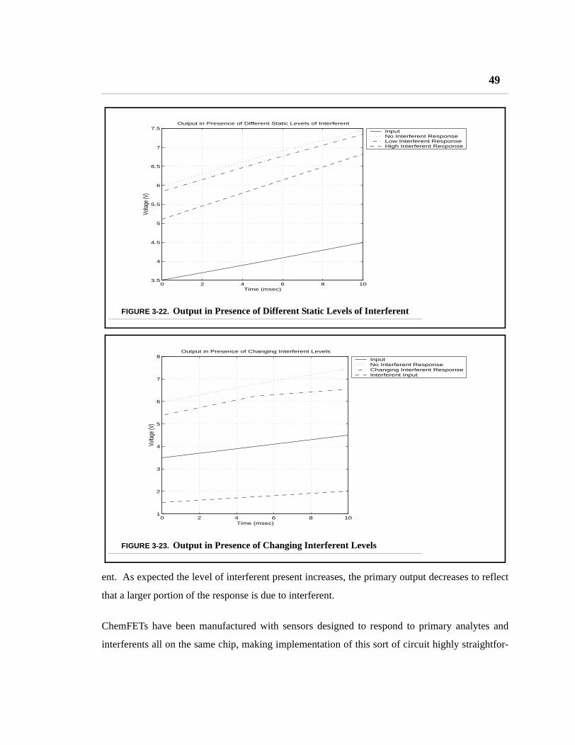
49
ent. As expected the level of interferent present increases, the primary output decreases to reflect
that a larger portion of the response is due to interferent.
ChemFETs have been manufactured with sensors designed to respond to primary analytes and
interferents all on the same chip, making implementation of this sort of circuit highly straightfor-
FIGURE 3-22. Output in Presence of Different Static Levels of Interferent
0 2 4 6 8 103.5
4
4.5
5
5.5
6
6.5
7
7.5
Time (msec)
Volta
ge (V
)
Output in Presence of Different Static Levels of Interferent
InputNo Interferent ResponseLow Interferent ResponseHigh Interferent Response
FIGURE 3-23. Output in Presence of Changing Interferent Levels
0 2 4 6 8 101
2
3
4
5
6
7
8
Time (msec)
Volta
ge (V
)
Output in Presence of Changing Interferent Levels
InputNo Interferent ResponseChanging Interferent ResponseInterferent Input
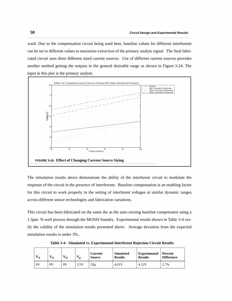
50 Circuit Design and Experimental Results
ward. Due to the compensation circuit being used here, baseline values for different interferents
can be set to different values to maximize extraction of the primary analyte signal. The final fabri-
cated circuit uses three different sized current sources. Use of different current sources provides
another method getting the outputs in the general desirable range as shown in Figure 3-24. The
input in this plot is the primary analyte.
The simulation results above demonstrate the ability of the interferent circuit to modulate the
response of the circuit in the presence of interferents. Baseline compensation is an enabling factor
for this circuit to work properly in the setting of interferent voltages at similar dynamic ranges
across different sensor technologies and fabrication variations.
This circuit has been fabricated on the same die as the auto-zeroing baseline compensator using a
1.5µm N-well process through the MOSIS foundry. Experimental results shown in Table 3-4 ver-
ify the validity of the simulation results presented above. Average deviation from the expected
simulation results is under 3%..
Table 3-4 - Simulated vs. Experimental Interferent Rejection Circuit Results
Vi1 Vi2 Vi3 Vp
Current Source
Simulated Results
Experimental Results
Percent Difference
0V 0V 0V 3.5V 32µ 4.01V 4.12V 2.7%
FIGURE 3-24. Effect of Changing Current Source Sizing
0 2 4 6 8 102
3
4
5
6
7
8
Time (msec)
Volta
ge (V
)
Effect of Changing Current Source Sizing with High Interferent Present
Input8u Current Source32u Current Source64u Current Source

51
0V 0V 0V 4.5V 32µ 2.55V 2.60V 2.0%
2V 2V 2V 3.5V 32µ 4.17V 4.20V 0.7%
2V 2V 2V 4.5V 32µ 2.66V 2.72V 2.3%
5V 5V 5V 3.5V 32µ 4.89V 4.95V 1.2%
5V 5V 5V 4.5V 32µ 3.18V 3.30 3.8%
3V 5V 7V 3.5V 32µ 4.75V 4.92 3.6%
3V 5V 7V 4.5V 32µ 3.09V 3.21 3.9%
5V 5V 5V 3.5V 8µ 7.51V 7.88 4.9%
5V 5V 5V 3.5V 64µ 4.35V 4.55 4.6%
Table 3-4 - Simulated vs. Experimental Interferent Rejection Circuit Results
Vi1 Vi2 Vi3 Vp
Current Source
Simulated Results
Experimental Results
Percent Difference

52 Circuit Design and Experimental Results

53
CHAPTER 4 System Integration and Summary
This chapter looks at system level applications of chemical sensors using the discrete auto-zeroing
baseline compensator. The automated nature of the discrete auto-zeroing baseline compensator as
well as its ability to compensate over a wide range and over chemiresistors and ChemFETs make it
a good candidate for use in system level applications. Future system applications using the inte-
grated auto-zeroing baseline compensation circuit should further improve results. Intelligent post-
processing using principal component analysis in combination with the reduced dynamic range
created by compensation creates a visual display of chemical sensor responses that can easily be
analyzed using built-in human classification abilities.
This chapter also includes suggested areas of research which could build on the results presented
in this research effort. Finally, the main points and results of this effort are concisely summarized
for reference purposes.
SECTION 4.1 TRANSIENT RESPONSE CHEMICAL DISCRIMINATION MODULE BACKGROUND
The portable chemical discrimination module combines arrays of homogeneous sensors for rea-
sons discussed in Chapter 3 to improve noise performance and detecting broken sensors with het-
erogeneous arrays of sensors to discriminate among analytes of interest. Sensors can be modularly
added to or removed from the measurement module. Using these sensors, the module supplies the
54 System Integration and Summary
user with real-time chemical discrimination information that tracks the response vector of the sen-
sor as it proceeds from baseline to its steady-state location in multidimensional sensor space. The
module includes slots for homogeneous arrays of sensors, heterogeneous arrays of sensors, plug-
and-play signal conditioning modules, and a microcontroller for converting normalized sensor sig-
nals for display in two-dimensional principal component space.
At the single sensor level, the signal conditioning circuits are designed to process chemical sensor
signals in such a way that similar dynamic range and baseline states are ensured at the output of the
sensor signal conditioning, regardless of sensor drift, type or fabrication variation. As discussed in
Chapter 3, baseline compensator circuits use a sensor calibration feedback loop to normalize sen-
sor baseline states, so that the response of each sensor begins at the same value. Auto-zeroing
baseline compensation ensures that the dynamic range of the sensor output is completely con-
sumed by response to analytes rather than to changes in baseline caused by variations in manufac-
turing. Removal of the effects of baseline variation reduces the number of bits required for a given
concentration resolution, thereby reducing power and cost requirements for the portable module.
SECTION 4.2 INTERCHANGEABLE SENSOR INTERFACE
As previously noted in Chapter 3, the compensation mechanism used here is largely sensor inde-
pendent. Three factors prevent this compensation technique from complete sensor-independence.
These factors are the impact of sensor settling, the range of values of the initial sensor baseline
parameters, and the value to which sensors of different types are to be compensated.
Rt governs the time that the compensation circuit is enabled. Disabling prevents compensation
from occurring when the sensor is legitimately changing in response to an analyte. The time t, in
seconds that the compensation circuit will be enabled based on a monostable timer is:
(Eq 4.1)
In general it has been observed and can be explained by sensor manufacturing techniques that
ChemFETs take longer to settle during compensation and so will require a longer enabling time
than the chemiresistors. In the context of the system block diagram, Rt affects the enable pin on
the counter in Figure 3-6.
t 1.1 10⋅ 6–Rt=
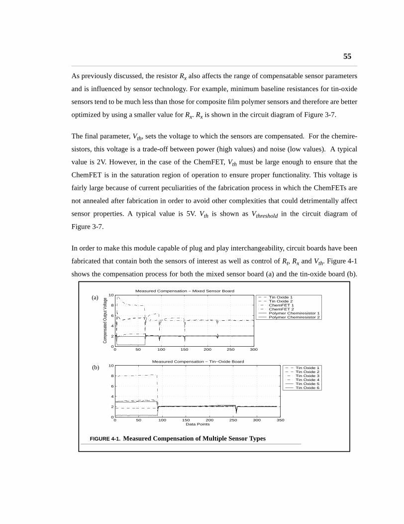
55
As previously discussed, the resistor Rx also affects the range of compensatable sensor parameters
and is influenced by sensor technology. For example, minimum baseline resistances for tin-oxide
sensors tend to be much less than those for composite film polymer sensors and therefore are better
optimized by using a smaller value for Rx. Rx is shown in the circuit diagram of Figure 3-7.
The final parameter, Vth, sets the voltage to which the sensors are compensated. For the chemire-
sistors, this voltage is a trade-off between power (high values) and noise (low values). A typical
value is 2V. However, in the case of the ChemFET, Vth must be large enough to ensure that the
ChemFET is in the saturation region of operation to ensure proper functionality. This voltage is
fairly large because of current peculiarities of the fabrication process in which the ChemFETs are
not annealed after fabrication in order to avoid other complexities that could detrimentally affect
sensor properties. A typical value is 5V. Vth is shown as Vthreshold in the circuit diagram of
Figure 3-7.
In order to make this module capable of plug and play interchangeability, circuit boards have been
fabricated that contain both the sensors of interest as well as control of Rt, Rx and Vth. Figure 4-1
shows the compensation process for both the mixed sensor board (a) and the tin-oxide board (b).
0 50 100 150 200 250 3000
2
4
6
8
10
Com
pens
ated
Out
put V
olta
ge
Measured Compensation − Mixed Sensor Board
Tin Oxide 1Tin Oxide 2ChemFET 1ChemFET 2Polymer Chemiresistor 1Polymer Chemiresistor 2
0 50 100 150 200 250 300 3500
2
4
6
8
10
Data Points
Measured Compensation − Tin−Oxide Board
Tin Oxide 1Tin Oxide 2Tin Oxide 3Tin Oxide 4Tin Oxide 5Tin Oxide 6
FIGURE 4-1. Measured Compensation of Multiple Sensor Types
(a)
(b)
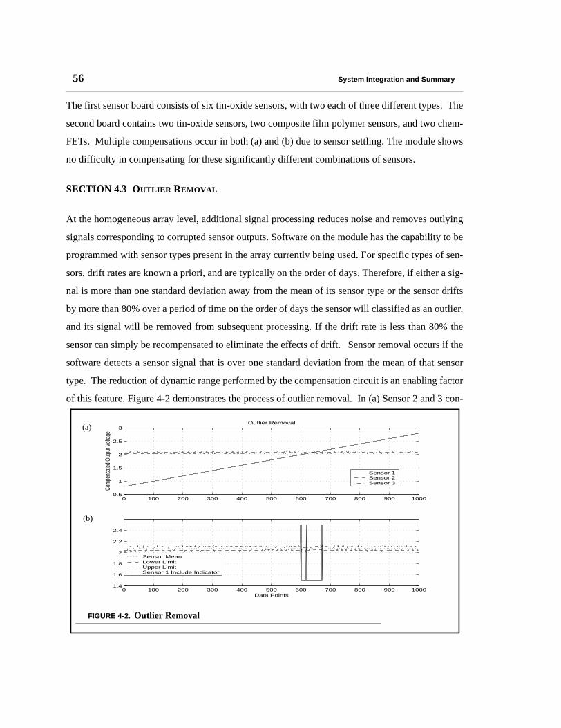
56 System Integration and Summary
The first sensor board consists of six tin-oxide sensors, with two each of three different types. The
second board contains two tin-oxide sensors, two composite film polymer sensors, and two chem-
FETs. Multiple compensations occur in both (a) and (b) due to sensor settling. The module shows
no difficulty in compensating for these significantly different combinations of sensors.
SECTION 4.3 OUTLIER REMOVAL
At the homogeneous array level, additional signal processing reduces noise and removes outlying
signals corresponding to corrupted sensor outputs. Software on the module has the capability to be
programmed with sensor types present in the array currently being used. For specific types of sen-
sors, drift rates are known a priori, and are typically on the order of days. Therefore, if either a sig-
nal is more than one standard deviation away from the mean of its sensor type or the sensor drifts
by more than 80% over a period of time on the order of days the sensor will classified as an outlier,
and its signal will be removed from subsequent processing. If the drift rate is less than 80% the
sensor can simply be recompensated to eliminate the effects of drift. Sensor removal occurs if the
software detects a sensor signal that is over one standard deviation from the mean of that sensor
type. The reduction of dynamic range performed by the compensation circuit is an enabling factor
of this feature. Figure 4-2 demonstrates the process of outlier removal. In (a) Sensor 2 and 3 con-
0 100 200 300 400 500 600 700 800 900 10000.5
1
1.5
2
2.5
3
Comp
ensa
ted O
utput
Volta
ge
Outlier Removal
Sensor 1Sensor 2Sensor 3
0 100 200 300 400 500 600 700 800 900 10001.4
1.6
1.8
2
2.2
2.4
Data Points
Sensor MeanLower LimitUpper LimitSensor 1 Include Indicator
FIGURE 4-2. Outlier Removal
(a)
(b)

57
tain real sensor data, while Sensor 1 is a simulated ramp. (b) shows the results of outlier removal
on the sensor average as Sensor 1 moves out of the acceptable range defined by one standard devi-
ation from the sensor mean for that type of sensor.
SECTION 4.4 PRINCIPAL COMPONENT ANALYSIS
This research effort uses principal component analysis to discriminate between different types of
analytes. Linear feature reduction methods in the past has been found to produce moderately
robust results with minimal computational burden while non-linear techniques like artificial neural
networks produce a more robust response, but at much greater computational expense [30]. Intelli-
gent pre-processing such as baseline compensation, noise filtering, and outlier removal have the
effect of enhancing the discrimination abilities of this module.
Figure 4-3 demonstrates initial results of principal component analysis, used here for analyte clas-
sification purposes. Data is taken using three different types of composite film polymer chemire-
sistors using no compensation, and using the integrated compensation circuit. The sensors are
placed in a sealed chamber into which the analyte is allowed to diffuse. Measurements continued
until the sensors reach a steady-state response. The figure shows the euclidean distance between
the two-dimensional principal component transformed data for responses to Methanol and Ammo-
nia. In this typical response the compensated sensors show an 11% improvement discriminating
ability.
FIGURE 4-3. Principal Component Analysis on Compensated and Uncompensated Sensors
0 20 40 60 80 100 120 140 1600.005
0.01
0.015
0.02
0.025
0.03
0.035
0.04
Data Points in Time
Euc
lidea
n D
ista
nce
Euclidean distance between sensor responses to Methanol and Ammonia based on PCA
CompensatedUncompensated
58 System Integration and Summary
Principal component analysis is then applied to the task of using compensation to build a transient
response chemical discrimination module. The primary objective of developing the chemical dis-
crimination module is to demonstrate the transient path of a sensor to its steady-state response vec-
tor to enhance the user’s ability to discriminate among analytes of interest. Visual presentation of
the data is accomplished via principal component projection of the multi-dimensional sensor data;
however, any data reduction system that retains salient discrimination information would be
appropriate for this type of system.
After signal conditioning, the outputs of the heterogeneous arrays are transferred to a microcon-
troller and a principal component transformation is applied to the multi-dimensional sensor data
for projection onto a portable display. Principal component analysis allows the subsequent extrac-
tion of analyte information from data in a highly efficient and compact manner. Using this type of
analysis to convert the data into principal component space, the data can be displayed on a two-
dimensional LCD screen. Pre-calibrated points for air and the analytes of interest are displayed on
the screen as well. Users are then able to watch in real-time as the point on the screen moves in
response to an applied chemical. In using a graphical display, this work takes advantage of the
built-in pattern recognition abilities in the human brain to estimate that a certain analyte may be
present if the data point on the screen is closer to one calibration point than others. The use of this
built-in pattern recognition ability drastically reduces circuit complexity and power requirements
while still supplying the needed information on chemical discrimination.
SECTION 4.5 EXPERIMENTAL RESULTS
The portable chemical discrimination system has been calibrated on multiple concentrations, up to
saturation, of methanol, formaldehyde, and ammonia and tested on multiple concentrations, up to
saturation, of methanol. Both tin-oxide sensor modules and mixed sensor modules have been used
on demonstrate the performance of the system for these analytes.
Figure 4-4 demonstrates the results of principal component analysis, used here for analyte classifi-
cation purposes. Data was taken using each of the two sensor boards described above. Calibration
data is shown for each of the three analytes, formaldehyde, ammonia, and methanol. (a) and (b)
represent a subsequent response to and recovery from methanol for the tin-oxide sensor board and

59
the mixed sensor board respectively. The path of the sensor response clearly traveled from the ini-
tial baseline area to the methanol calibration point, thereby revealing the analyte to which the mod-
ule was responding. In (a) the separation between analyte clusters is well-defined. Upon recovery,
the signal approaches baseline conditions. Reasons for incomplete recovery include the need for a
longer recovery time, or sensor drift, which could easily be compensated using the auto-zeroing
baseline compensation circuit. In (b) the analyte clusters are not very well defined. This feature
illustrates an important point. The composite-film polymer chemiresistors chosen for this sensor
array are not very responsive to any of the analytes chosen. This lack of response decreased the
amount of variance which the principal component analysis had to work with, and thereby limit
the classification ability. Large mixed sensor arrays have the potential to act as better classifiers
because they can potentially be responsive to more analytes and analyte families to varying
degrees, but sensor types must be chosen wisely. In both cases, a user of the module can watch as
the response path approaches a cluster and using their own abilities as a classifier, make a decision
as to what chemical is present.
Figure 4-5 shows a sample display screen for the chemical module. Software features are included
for resetting the compensation process, dictating when the sensors are at baseline conditions and
0.5 1 1.5 2 2.5 3 3.5 4 4.5 5−1.5
−1
−0.5
0
0.5
1
Princ
ipal C
ompo
nent
2
PCA of Methanol Response and Recovery − Tin−Oxide Sensor Board
7.6 7.65 7.7 7.75 7.8 7.85 7.9 7.95 8−0.5
0
0.5
1
1.5
2
2.5
Principal Component 1
PCA of Compensated Response and Recovery − Mixed Sensor Board
Ammonia Cluster
Methanol Cluster
Formaldehyde Cluster
Ammonia Cluster
Formaldehyde Cluster
Methanol Cluster
Baseline Conditions
Baseline Conditions
FIGURE 4-4. Principal Component Analysis Experimental Results
(a)
(b)

60 System Integration and Summary
for starting and stopping the PCA display. In this sample screen shot, the sensor response travels
from initial baseline conditions to the methanol calibration cluster, which is well separated the
ammonia calibration cluster. The three voltages at the bottom of the screen represent average
response voltages for the three different tin-oxide sensor types. The original baseline voltage was
2V. Figure 4-6 shows the entire transient response chemical discrimination module. A small fan on
the side of the box helps to deliver analyte to the sensors in a controlled manner. The entire box
weighs under five pounds. Battery power enables the box to operate continuously for over two
hours in the field. Three 9V Nickel Metral-Hydride battery packs are used to provide for a +18V
and -9V supply for the various circuit components. The batteries have a rating of 2000 mAh.
FIGURE 4-5. Sample Module Screen Shot
FIGURE 4-6. Transient Response Module

61
SECTION 4.6 SUGGESTED FUTURE AREAS OF RESEARCH
Many areas of research could continue directly from and benefit from the work presented here.
For example, future work on the compensation circuit includes adding averaging directly onto the
integrated circuit, especially for the case of linearly responding sensors, to process homogenous
arrays of sensors for a more robust aggregate output. Recall from Equation 2.4 that for composite
polymer sensors of the same type, the constant k will be the same for each analyte for one type of
sensor. The differing baseline resistance is not a factor in this equation due to the baseline compen-
sation. Therefore, because of the linear response, independent of baseline resistance, responses of
different sensors of the same type can be averaged together for a more robust response. Averaging
and other statistical methods can also be used to eliminate defective sensors by comparing an indi-
vidual sensor’s response with the average. Finally, to further reduce noise, the signal can be aver-
aged over time using appropriate filtering techniques. Currently, much of this averaging, filtering,
and outlier removal is performed externally by digital circuitry. Optimized on-chip analog cir-
cuitry should improve performance. Converting the sensor signals to currents rather than voltages
through a transduction amplifier, would put the signals in a form that are easily averaged, added,
and removed as appropriate.
Another simplification beyond merely integrating the compensation circuit is to incorporate float-
ing-gate technology in such a way that overcomes the drawbacks previously presented [12]. Cur-
rently the compensation circuit achieves baseline-compensation using an elaborately large
feedback loop composed of counters, digital to analog converters and comparators. The current
circuit requires that each sensor have its own complete compensation circuit. However, floating
gate technology can reduce the size of the integrated compensation circuit by two orders of magni-
tude by using floating-gate technology as analog memory [32]. By keeping the same compensation
scheme as described in previous sections, but adding analog memory, the signal will not be dis-
torted as in previous attempts [12]. Floating gate technology will also allow most of the compensa-
tion circuit to be reused for each sensor pixel thereby further reducing size. Having a small,
functional compensation circuit will enable the optimization of a large number of these chemical
sensors into a small, inexpensive, low-power, mobile chemical sensor unit.
62 System Integration and Summary
Many improvements are possible in the transient response module as well. For example, software
can be improved to enable analyte calibration points to be added in the field rather than in the lab-
oratory. Calibration points taken in the field are more accurate because they take into account field
conditions such as humidity and temperature.
SECTION 4.7 SUMMARY
This research effort has described and detailed the development of the auto-zeroing baseline com-
pensation circuit and other associated sensor signal processing such as noise filtering, outlier
removal, and principle component analysis. The final integrated version of the circuit is an
improvement of previous versions of the circuit in terms of accuracy, power requirements, applica-
bility to multiple sensor types, reduced volume, and reduced cost. This circuit as designed directly
compensates for variability in sensor manufacturing, sensor drift, variations in environmental
parameters, and sensor poisoning, as well eliminating high-frequency sensor noise. The reduction
in sensor dynamic range by this circuit has been shown to provide up to a factor of 34 improve-
ment in response resolution for typical sensor arrangements.
Other research efforts have taken different approaches to these inherent chemical sensor problems,
each with different disadvantages. For example, in the case of compensating for sensor drift, other
researchers propose using a complicated combination of principal component analysis and artifi-
cial neural networks [33] or adjusting making complicated adjustments to the PCA transformation
matrixes as the sensors drift over time by eliminating the first principal component [34]. The first
solution has the disadvantages of adding greatly to the circuit complexity and training complexity.
The second solution may not be valid, because drift may not always occur in the first two principal
components and the drift direction changes depending on the history and composition of applied
analytes.
Other attempts to build electronic noses have tended to use one type of sensor (e.g. only metal-
oxide sensors [35] or only conducting polymer sensors [36]). In addition, these electronic noses
tend to be calibrated for one specific use, such as discriminating among olive oil types [35] or
monitoring aromatic hydrocarbons [36]. The compensation circuit described in this chapter along
with intelligent post-processing allows for multiple sensor types to be used together in a much sim-

63
pler fashion than has been previously available, to the point where sensors of different types may
be interchanged. Flexibility in creating sensor arrays, and the ability to compensate out deleterious
sensor artifacts will lead to more general-purpose applications for electronic noses.
Experimental results have shown that baseline compensation is possible with sensors over wide
manufacturing variability. Different types of compensation methods and designs have been dis-
cussed and compared, with the integrated variable current source compensator shown to have
overall superior results with potential for further improvement. The integrated compensator has
been shown to be able to maintain a constant current output over varying loading, with less than
0.6% deviation from a constant current with a load change of as much as 25%. Compensation to
within 0.5% of desired baseline output voltages has been demonstrated using the two stage design.
Drift in the current source was shown to be negligible over a period of over 24 hours. Typical sen-
sor drift compensation results were shown in which subsequent to the sensor drifting, compensa-
tion returned the sensor to within 0.03% of the original baseline value thus preserving output
dynamic range without affecting sensor sensitivity or response characteristic. Compensation to a
desired baseline output for a wide range of initial sensor values was shown with an error of less
than 5%. Typical results also demonstrated that the integrated compensation circuit allowed a
minimum analyte detection limit twice as good as that of more traditional sensor signal extraction
methods. Finally, preliminary principal component analysis demonstrates an 11% improvement in
analyte discrimination ability using this compensation scheme.
Also, an interferent rejection circuit has been shown both in simulation and experiment to increase
response accuracy. The circuit separates out the effect of interferents on the output compared to
the response to the primary analyte.
In addition, the ability of a modular and portable chemical discrimination system to track and dis-
play response paths of multidimensional sensor arrays in principal component space has been
demonstrated. The modules are designed to be low power to achieve low-power objectives and
principal component analysis does not overload the low-power microcontroller (PIC 16F877) in
this low-overhead system. Response paths have been shown on the module in calibration and
tested to be easily identified with the human eye for three different analytes. The ability to inter-
change sensors of the same or different types and to compensate for unknown baseline conditions

64 System Integration and Summary
has been demonstrated. Simple noise removal techniques and outlier removal have also been used
to improve the classification ability of the module. The end result is a portable box that a user can
take with them into the field to search for pre-calibrated analytes using intuitive human-oriented
classification methods.
Intelligent pre-processing of chemical sensor signals have been shown to reduce the effects of sen-
sor variability and to enhance the abilities of signal post-processing to discriminate among ana-
lytes.
References
References
[1] Beth C. Mu oz et al., “Conductive polymer-carbon black composites-based sensor arrays for use in an electronic nose,” Sensor Review 19, No. 4, pp. 300-305, 1999.
[2] D. M. Wilson, S. Hoyt, J. Janata, K. Booksh, L. Obando, “Chemical sensors for portable, handheld field instruments,” IEEE Sensors Journal 1, No. 4, pp. 256-274, 2001.
[3] Kousuke Ihokura and Joseph Watson, The Stannic Oxide Gas Sensor, pp. 49-88, CRC Press, Ann Arbor, 1994.
[4] E. Llobet et. al, “Electrical equivalent models of semiconductor gas sensors using PSPICE,” Sensors and Actuators B 77 pp. 275-280, 2001.
[5] Janata, Jiri and Huber, Robert J., Principles of Chemical Sensors, pp. 152-174, Academic Press, New York, 1985.
[6] J. Janata, M. Josowicz, “Chemical Modulation of Work Function as a Transduction Mechanism for Chemical Sensors,” Accounts of Chemical Research 31, No. 5, pp. 241-248, 1998.
[7] Russell D. Reed and Robert J. Marks II, Neural Smithing, pp. 299-310, The MIT Press, Cambridge, MA, 1999.
[8] Erik J. Severin et al., “An Investigation of the Concentration Dependence and Response to Analyte Mixtures of Carbon Black/Insulating Organic Polymer Composite Vapor Detectors,” Analytical Chemistry 72, pp. 658-668, 2000.
[9] Mark C. Lonergan, Erik J. Severin, Brett J. Doleman, Sara A. Beaber, Robert H. Grubbs, and Nathan S. Lewis, “Array-Based Vapor Sensing Using Chemically Sensitive, Carbon-Black-Polymer Resistors,” Chem-istry of Materials 8, No. 9, pp. 2298-2312, 1996.
[10] C. Di Natale et al., “Comparison and integration of arrays of quartz resonators and metal-oxide semi-conductor chemoresistors in the quality evaluation of olive oils,” Sensors and Actuators B 78, pp. 303-309, 2001.
[11] J. Boris, “The threat of chemical and biological terrorism: preparing a response,” Computing in Science and Engineering 4, No. 2, pp. 22-32, 2002.
[12] Alyssa Apsel, Theron Stanford and Paul Hasler, “An Adaptive Front End for Olfaction,” ISCAS '98, Proceedings of the 1998 IEEE International Symposium on Circuits and Systems 3, pp. 107-110, 1998.
[13] J. V. Hatfield and P. I. Neaves, “A Signal Processing ASIC for an Electronic Nose,” IEE Colloquium on Application Specific Integrated Circuits for Measurement Systems, pp. 8/1 -8/5, 1994.
[14] J. Brezmes et. al., “Application of Artificial Neural Networks to the Design and Implementation of Electronic Olfactory Systems,” NEUREL-2000, Proceedings of the 5th Seminar on Neural Network Applica-tions in Electrical Engineering, pp. 75-80, Belgrade, Yugoslavia, 2000.
[15] “Terra: The EOS Flagship”, http://terra.nasa.gov.
[16] Sam McKennoch, D.M. Wilson, “Autoranging Compensation for Variable Baseline Chemical Sensors”, Proc. SPIE Int’l Symp. Env. Ind. Sensing, Boston, MA, 2001.
[17] Sam McKennoch, D.M. Wilson, “Electronic Interface Modules for Solid-State Chemical Sensors”, Proc. IEEE Sensors, Orlando, FL, 2002.
n
67

[18] Sean Hoyt, Sam McKennoch, D.M. Wilson, “Transient Response Chemical Discrimination Module”, Proc. IEEE Sensors, Orlando, FL, 2002.
[19] Ishnida, H., Nakamoto, T., and Moriizumi, T., “Remote sensing and localization of gas/odor source and distribution using mobile sensing system,” Proceedings of the 1997 International Conference on Solid-State Sensors and Actuators, Transducers ‘97, Chicago, IL, 1997.
[20] B. Lundberg and B. Sundquist, “Resistivity of a composite conducting polymer as a function of temper-ature, pressure, and environment: Application as a pressure and gas concentration transducer,” Journal of Applied Physics 60, No. 3, pp. 1074-1079, August 1, 1986.
[21] R. D. Sherman et al., “Electron Transport Processes in Conductor-Filled Polymers,” Polymer Engineer-ing and Science 23, No. 1, pp. 36-46, 1983.
[22] B. Doleman et al., “Quantitative Study of the Resolving Power of Arrays of Carbon Black-Polymer Composites in Various-Sensing Tasks,” Analytical Chemistry 70, pp. 4177-4190, 1998.
[23] John P. Uyemura, CMOS Logic Circuit Design, pp. 113-140, Kluwer Academic Publishers, Boston, 1999.
[24] Chao-Ming Ying and Babu Joseph, “Sensor Fault Detection Using Noise Analysis,” Ind. Eng. Chem. Res. 39, No. 2, pp. 396-407, 2000.
[25] Paul R. Gray and Robert G. Meyer, Analysis and Design of Analog Integrated Circuits, pp. 635-667, John Wiley & Sons, Inc., New York, 1977.
[26] H. V. Shurmer, P. Corcoran, M. K. James, Sens. Actuators B 1993, 16, 256.
[27] Julian Gardner, Microsensors: Principles and Applications, pp. 19-30, John Wiley & Sons, Inc., New York, 1994.
[28] M. Pardo et al., “Data preprocessing enhances the classification of different brands of Espresso coffee with an electronic nose,” Sens. Actuators B 69, pp. 397-403, 2000.
[29] R. Ionescu, A. Vancu, and A. Tomescu, “Time-dependant humidity calibration for drift corrections in electronic noses equipped with SnO2 gas sensors,” Sens. Actuators B 69, pp. 283-286, 2000.
[30] Denise M. Wilson and Thaddeus A. Roppel, “Hardware Architectures for Chemical Sensing Electron-ics,” Proceedings of the SPIE Conference on Internal Standardization and Calibration Architectures for Chemical Sensors, Boston, MA, 1999.
[31] Leslie M. Kay and Gilles Laurent, “Odor- and context-dependent modulation of mitral cell activity in behaving rats,” Nature Neuroscience 2 No. 11, pp. 1003-1009, 1999.
[32] R. R. Harrison et al., “A CMOS programmable analog memory-cell array using floating-gate circuits,” Circuits and Systems II: Analog and Digital Signal Processing, IEEE Transactions on, 48, Issue 1, pp. 4-11, January 2001.
[33] M. Holmberg et al., “Drift counteraction for an electronic nose,” Sens. Actuators B 35/36, pp. 528-535, 1996.
[34] A. C. Romain, Ph. Andre, and J. Nicolas, “Three year experiment with the same tin oxide sensor arrays for the identification of malodorous sources in the environment,” Sens. Actuators B 84, pp. 271-277, 2002.
[35] M. Concepcion Cerrato Oliveros et al., “Electronic nose based on metal oxide semiconductor sensors as a fast alternative for the detection of adulteration of virgin olive oils,” Analytica Chimica Acta 459, pp. 219-228, 2002.
68

References
[36] Joseph N. Barisci et al., “Conducting polymer sensors for monitoring aromatic hydrocarbons using an electronic nose,” Sensors and Actuators B 84, pp. 252-257, 2002.
69

70
Acknowledgements
The author wishes to express sincere appreciation to the following people: Dr. Nathan Lewis for
providing composite-film polymer sensors; Dr. Jiri Janata and Brian Polk for providing Chem-
FETs and advice on their use; Sean Hoyt for his work on the digital aspects of the transient-
response chemical discrimination module; Dr. Bruce Darling for taking the time to be on my com-
mittee; all my co-workers in the DMS lab for their encouragement; Carola for the sacrifices she
made to enable me to proceed through my graduate career; and my advisor Dr. Denise Wilson for
providing the opportunity to undertake this effort in the first place, and for her guidance and moti-
vation over the past two years. Without those listed above this thesis would not have been possi-
ble.
lxix

lxx


