AUDIO MODULATED MATRIX LED DRIVER - ISSI · · 2017-05-30AUDIO MODULATED MATRIX LED DRIVER...
13
IS31FL3728 Integrated Silicon Solution, Inc. – www.issi.com 1 Rev.B, 15/11/2016 AUDIO MODULATED MATRIX LED DRIVER November 2016 GENERAL DESCRIPTION IS31FL3728 is a general purpose 8×8 LED matrix driver which features an audio frequency equalizer (EQ) mode or a general LED dot matrix display mode. The general LED matrix display defaults to an 8×8 configuration, however, it can be configured for a 5×11, 6×10, 7×9 dot matrix display. The matrix picture brightness can be modulated by audio. In either the audio EQ mode or matrix display mode, the array is internally scanned, and requires only one-time programming, thus eliminating the need for real time system resource utilization. It programs the LED array through I2C interface. In the general purpose display mode, each dot of the LED array is independently programmed on or off over time. In the audio EQ mode, the X axis (column) represents the frequency bands while the Y axis (row) represents the strength of the input audio signal in each band. The number of LEDs lit in a column is proportional to the strength of the audio signal in the corresponding band in a thermometer-coded manner. IS31FL3728 is available in 24-pin QFN (4mm × 4mm). It operates from 2.7V to 5.5V over the temperature range of -40°C to +85°C (IS31FL3728-QFLS2-TR), -40°C to +105°C (IS31FL3728-QFLS3-TR). FEATURES 5~8 current source outputs for row control 8~11 outputs for column scan control Programmable 8×8, 7×9, 6×10, 5×11 matrix One-time programming, internal scan Full scale LED current controlled by internal register setting or audio signal Audio frequency EQ display with programmable input gain LED matrix brightness can be modulated with audio Signal One address pin with 4 logic levels to allow four I2C slave addresses I2C interface 2.7V to 5.5V supply Over-temperature protection QFN-24 (4mm × 4mm) package APPLICATIONS Mobile phones and other hand-held devices for LED displays. Audio frequency equalizer display TYPICAL APPLICATION CIRCUIT SDA SCL AD IN C_FILT SDB IS31FL3728 R1 R2 R3 R4 R5 C1 C2 C3 C4 C5 C6 C7 C8 R8/C9 R7/C10 R6/C11 0.22μF 0.1μF VBattery VCC Audio In 1μF 0.1μF Micro Controller 4.7kΩ 4.7kΩ 100kΩ VDD 11 1 2 3 4 5 6 20 22 15 14 13 12 10 9 8 7 21 19 18 17 16 23 24 GND Figure 1 Typical Application Circuit
Transcript of AUDIO MODULATED MATRIX LED DRIVER - ISSI · · 2017-05-30AUDIO MODULATED MATRIX LED DRIVER...

IS31FL3728
Integrated Silicon Solution, Inc. – www.issi.com 1 Rev.B, 15/11/2016
AUDIO MODULATED MATRIX LED DRIVER
November 2016
GENERAL DESCRIPTION
IS31FL3728 is a general purpose 8×8 LED matrix driver which features an audio frequency equalizer (EQ) mode or a general LED dot matrix display mode. The general LED matrix display defaults to an 8×8 configuration, however, it can be configured for a 5×11, 6×10, 7×9 dot matrix display. The matrix picture brightness can be modulated by audio. In either the audio EQ mode or matrix display mode, the array is internally scanned, and requires only one-time programming, thus eliminating the need for real time system resource utilization.
It programs the LED array through I2C interface. In the general purpose display mode, each dot of the LED array is independently programmed on or off over time. In the audio EQ mode, the X axis (column) represents the frequency bands while the Y axis (row) represents the strength of the input audio signal in each band. The number of LEDs lit in a column is proportional to the strength of the audio signal in the corresponding band in a thermometer-coded manner.
IS31FL3728 is available in 24-pin QFN (4mm × 4mm). It operates from 2.7V to 5.5V over the temperature range of -40°C to +85°C (IS31FL3728-QFLS2-TR), -40°C to +105°C (IS31FL3728-QFLS3-TR).
FEATURES
5~8 current source outputs for row control
8~11 outputs for column scan control
Programmable 8×8, 7×9, 6×10, 5×11 matrix
One-time programming, internal scan
Full scale LED current controlled by internal register setting or audio signal
Audio frequency EQ display with programmable input gain
LED matrix brightness can be modulated with audio Signal
One address pin with 4 logic levels to allow four I2C slave addresses
I2C interface
2.7V to 5.5V supply
Over-temperature protection
QFN-24 (4mm × 4mm) package
APPLICATIONS
Mobile phones and other hand-held devices for LED displays.
Audio frequency equalizer display
TYPICAL APPLICATION CIRCUIT
SDA
SCL
AD
IN
C_FILT
SDB
IS31FL3728
R1
R2
R3
R4
R5
C1
C2
C3
C4
C5
C6
C7
C8
R8/C9
R7/C10
R6/C11
0.22μF
0.1μF
VBattery
VCC
Audio In
1μF 0.1μF
Micro
Controller
4.7kΩ 4.7kΩ
100kΩ
VDD
11
1
2
3
4
5
6
20
22
15
14
13
12
10
9
8
7
21
19
18
17
16
23
24
GND
Figure 1 Typical Application Circuit

IS31FL3728
Integrated Silicon Solution, Inc. – www.issi.com 2 Rev.B, 15/11/2016
PIN CONFIGURATION
Package Pin Configuration (Top View)
QFN-24
1
2
3
4
24
14
15
16
17
23
22
21
7 8 9 10
5
11
18
20
6
12
13
19
R1
R2
R3
R4
VC
C
R5
R6/C11
R7/C10
R8/C9
C8
C7
C6
SDB
AD
IN
C_FILT
SCL
SDA
C5
GN
D
C4
C3
C2
C1
PIN DESCRIPTION
No. Pin Description
1 SDA Serial data.
2 SCL Serial clock.
3 SDB Shutdown the chip when pull to low.
4 IN Audio input.
5 C_FILT Low pass filter cap for audio control.
6 AD I2C Address setting.
7~10, 12 R1~R5 Current source outputs.
11 VCC Power supply.
13~15 R6/C11, R7/C10, R8/C9 CMOS outputs.
16~19,21~24 C8~C1 Current sink outputs.
20 GND Ground.
Thermal Pad Connect to GND.
Copyright © 2016 Integrated Silicon Solution, Inc. All rights reserved. ISSI reserves the right to make changes to this specification and its products at any time without notice. ISSI assumes no liability arising out of the application or use of any information, products or services described herein. Customers are advised to obtain the latest version of this device specification before relying on any published information and before placing orders for products. Integrated Silicon Solution, Inc. does not recommend the use of any of its products in life support applications where the failure or malfunction of the product can reasonably be expected to cause failure of the life support system or to significantly affect its safety or effectiveness. Products are not authorized for use in such applications unless Integrated Silicon Solution, Inc. receives written assurance to its satisfaction, that: a.) the risk of injury or damage has been minimized; b.) the user assume all such risks; and c.) potential liability of Integrated Silicon Solution, Inc is adequately protected under the circumstances

IS31FL3728
Integrated Silicon Solution, Inc. – www.issi.com 3 Rev.B, 15/11/2016
ORDERING INFORMATION
Industrial Range: -40°C to +85°C
Order Part No. Package QTY/Reel
IS31FL3728-QFLS2-TR QFN-24, Lead-free 2500
Industrial Range: -40°C to +105°C
Order Part No. Package QTY/Reel
IS31FL3728-QFLS3-TR QFN-24, Lead-free 2500

IS31FL3728
Integrated Silicon Solution, Inc. – www.issi.com 4 Rev.B, 15/11/2016
ABSOLUTE MAXIMUM RATINGS
Supply voltage, VCC -0.3V ~ +6.0V
Voltage at any input pin -0.3V ~ VCC+0.3V
Maximum junction temperature, TJMAX 150°C
Storage temperature range, TSTG -65°C ~ +150°C
Operating temperature range, TA = TJ −40°C ~ +85°C, IS31FL3728-QFLS2-TR −40°C ~ +105°C, IS31FL3728-QFLS3-TR
Junction to ambient, θJA 40°C/W
ESD (HBM)
ESD (CDM)
±4KV ±1KV
Note:
Stresses beyond those listed under “Absolute Maximum Ratings” may cause permanent damage to the device. These are stress ratings only and functional operation of the device at these or any other condition beyond those indicated in the operational sections of the specifications is not implied. Exposure to absolute maximum rating conditions for extended periods may affect device reliability.
ELECTRICAL CHARACTERISTICS
The following specifications apply for VCC = 5V, TA = 25°C, unless otherwise noted.
Symbol Parameter Condition Min. Typ. Max. Unit
VCC Supply voltage 2.7 5.5 V
ICC Quiescent power supply current
VIN = 0V, register CD1:CD11 = 0 dot matrix display mode without audio modulation
4.1 5.0 mA
ISD Shutdown current
VSDB = 0V 1.7 5.0 μA
VSDB = 5V Software Shutdown
1.7 5.0 μA
IOUT Output current of R1~R8
Dot matrix display mode without audio modulation
42.8
(Note 1) mA
Dot matrix display mode with audio modulation VIN = 1.5Vp-p, 1kHz square wave, audio gain = 0dB
42.3
(Note 1) mA
VHR
Current sink (ISINK, C1:C8) headroom voltage and current source (IOUT, R1:R8) headroom voltage
ISINK = 320mA (Note 2) 300
mV IOUT = 40mA 200
Logic electrical characteristics
VIN(0) Logic “0” input voltage VCC = 2.7V 0.4 V
VIN(1) Logic “1” input voltage VCC = 5.5V 1.4 V
IIN(0) Logic “0” input current VIN = 0V 5
(Note 3) nA
IIN(1) Logic “1” input current VIN = VCC 5
(Note 3) nA

IS31FL3728
Integrated Silicon Solution, Inc. – www.issi.com 5 Rev.B, 15/11/2016
DIGITAL INPUT SWITCHING CHARACTERISTICS (Note 3)
Symbol Parameter Condition Min. Typ. Max. Unit
fSCL Serial-Clock Frequency 400 kHz
tBUF Bus Free Time Between a STOP and a START Condition
1.3 μs
tHD, STA Hold Time (Repeated) START Condition 0.6 μs
tSU, STA Repeated START Condition Setup Time 0.6 μs
tSU, STO STOP Condition Setup Time 0.6 μs
tHD, DAT Data Hold Time 0.9 μs
tSU, DAT Data Setup Time 100 ns
tLOW SCL Clock Low Period 1.3 μs
tHIGH SCL Clock High Period 0.7 μs
tR Rise Time of Both SDA and SCL Signals, Receiving
(Note 4) 20 + 0.1Cb 300 ns
tF Fall Time of Both SDA and SCL Signals, Receiving
(Note 4) 20 + 0.1Cb 300 ns
Note 1: Current of Single LED in Rx(x=1~8) is IOUT/8. Note 2: All Row Drivers are ON. Note 3: Guaranteed by design. Note 4: Cb = total capacitance of one bus line in pF. ISINK ≤ 6mA. tR and tF measured between 0.3 × VCC and 0.7 × VCC.

IS31FL3728
Integrated Silicon Solution, Inc. – www.issi.com 6 Rev.B, 15/11/2016
DETAILED DESCRIPTION
I2C INTERFACE
The IS31FL3728 uses a serial bus, which conforms to the I2C protocol, to control the chip’s functions with two wires: SCL and SDA. The IS31FL3728 has a 7-bit slave address (A6:A0). The bit A1 and bit A0 are decided by the connection of AD pin.
The complete slave address is:
Table 1 Slave Address (Write only)
AD connects to
A6:A2 A1 A0 R/W____
GND
11000
0 0
0
(write only)
VCC 1 1
SCL 0 1
SDA 1 0
The SCL line is uni-directional. The SDA line is bi-directional (open-collector) with a pull-up resistor (typically 4.7kΩ). The maximum clock frequency specified by the I2C standard is 400 kHz. In this discussion, the master is the microcontroller and the slave is the IS31FL3728.
The timing diagram for the I2C is shown in Figure 3. The SDA is latched in on the stable high level of the SCL and the SDA line should be held high when not in use.
The “start” signal is generated by lowering the SDA signal while the SCL signal is high. The start signal will
alert all devices attached to the I2C bus to check the incoming address against their own chip address.
The 8-bit chip address is sent next, most significant bit first. Each address bit must be stable while the SCL level is high.
After the last bit of the chip address is sent, the master checks for the IS31FL3728’s acknowledge. The master releases the SDA line high (through a pull-up resistor). Then the master sends an SCL pulse. If the IS31FL3728 has received the address correctly, then it holds the SDA line low during the SCL pulse. If the SDA line is not low, then the master should send a “stop” signal (discussed later) and abort the transfer.
Following acknowledge of IS31FL3728, the register address byte is sent, most significant bit first. IS31FL3728 must generate another acknowledge indicating that the register address has been received.
Then 8 bits of data byte is sent, most significant bit first. Each data bit should be valid while the SCL level is stable high. After the data byte is sent, the IS31FL3728 must generate another acknowledge indicating that the data has been received.
If the master has more data bytes to send to the IS31FL3728, then the master can repeat the previous two steps until all data bytes have been sent.
The “stop” signal ends the transfer. To signal “stop”, the SDA signal goes high while the SCL signal is high.
A7 A6 A5 A4 A3 A2 A1 A0 A A7 A6 A5 A4 A3 A2 A11 2 3 4 5 6 7 8 9 1 2 3 4 5 6 7 8 9
S
A0 A D7 D6 D5 D4 D3 D2 D11 2 3 4 5 6 7 8 9
D0 A
P
IS31FL3728 Address Byte Register Address Byte Data Byte
Ack
by
IS31FL3728
SDA
SCL
Ack
by
IS31FL3728
Ack
by
IS31FL3728
Stop
by
Master
Figure 2 Writing to IS31FL3728
SDA
SCL
tHD,STA
tLOW
tHIGH
tSU,DAT tHD,DAT
tR tF
tSU,STA tHD,STA tSU,STO tBUF
S R P
Start Condition Restart Condition Stop Condition Start Condition
Figure 3 Interface Timing
Data Line Stable
Data Valid
Change of Data
Allowed
SDA
SCL
Figure 4 Bit Transfer

IS31FL3728
Integrated Silicon Solution, Inc. – www.issi.com 7 Rev.B, 15/11/2016
REGISTERS DEFINITION 00h Configuration Register
Bit D7 D6:D3 D2 D1 D0
Name SSD - Audio_EN ADM
Default 0 0000 0 0 0
The Configuration Register sets operation mode of IS31FL3728.
SSD Software Shutdown Enable
0 Normal Operation
1 Software Shutdown Mode
Audio_EN Audio Input Enable
0 Matrix Intensity is Controlled By The Current Setting In The Lighting Effect Register (0Dh)
1 Enable Audio Signal To Modulate The Intensity Of The Matrix In Dot Matrix Display Mode
ADM Array Mode Selection
00 8×8 Dot Matrix Display Mode
01 7×9 Dot Matrix Display Mode
10 6×10 Dot Matrix Display Mode
11 5×11 Dot Matrix Display Mode
01h~0Bh Column Data Register (CD1~CD11)
Bit D7:D0
Name R8:R1
Default 00000000
The column data registers store the on or off state of each LED in the array.
Rx LED State 0 LED Off 1 LED On
The data in the column data registers is valid only when the chip is configured in general purpose dot matrix display mode. 11 registers are assigned to CD1~CD11 columns respectively; the LED at a particular (row, column) location will be turned on when the respective data is set to 1. When configured to other than 8×8 dot matrix display mode operation, only the required number of LSBs is used in each column register. For example, in 5×11 dot matrix display mode, only bits R5 through R1 are used, and bits R8 through R6 are ignored.
0Ch Update Column Register
The data sent to the column data registers will be stored in temporary registers. A write operation of any 8-bit value to the Update Column Register is required to update the Column Data Registers (01h: 0Bh).
0Dh Lighting Effect Register
Bit D7 D6:D4 D3:D0
Name - AGS CS
Default 0 000 0000
The Lighting Effect Register stores the intensity control settings for all of the LEDs in the array
AGS Audio Input Gain Selection
000 0dB
001 +3dB
010 +6dB
011 +9dB
100 +12dB
101 +15dB
110 +18dB
111 -6dB
CS Full Current Setting For Each Row Output
0000 40mA
0001 45mA
... ...
0111 75mA
1000 5mA
1001 10mA
... ...
1110 35mA
0Fh Audio_EQ Register
Bit D7 D6 D5:D0
Name - AE_EN -
Default 0 0 000000
The Audio_EQ Register enables the audio frequency equalizer (audio EQ) mode
AE_EN Audio EQ Mode
0 Disable
1 Enable
IS31FL3728
Integrated Silicon Solution, Inc. – www.issi.com 8 Rev.B, 15/11/2016
APPLICATION INFORMATION
AUDIO FREQUENCY EQUALIZER (AUDIO EQ) MODE
The IS31FL3728 features audio frequency equalizer mode, or audio EQ mode.
The current of the matrix is adjusted by Lighting Effect Register as dot matrix display mode.
In the audio EQ mode, only 8 columns are valid and display the three bands of the audio signal. When the IS31FL3728 is configured as 7×9, 6×10 or 5×11, only columns C1 thru C8 will be used, and the remaining columns will always be off.
SDA
SCL
AD
IN
C_FILT
SDB
IS31FL3728
R1
R2
R3
R4
R5
C1
C2
C3
C4
C5
C6
C7
C8
R8/C9
R7/C10
R6/C11
0.22μF
0.1μF
VBattery
VCC
Audio In
1μF 0.1μF
Micro
Controller
4.7kΩ 4.7kΩ
100kΩ
VDD
11
1
2
3
4
5
6
20
22
15
14
13
12
10
9
8
7
21
19
18
17
16
23
24
GND
Audio Band
Sig
na
l S
tren
gth
Low Frequency High Frequency
Figure 5 Audio EQ Mode
GENERAL PURPOSE DOT MATRIX DISPLAY MODE
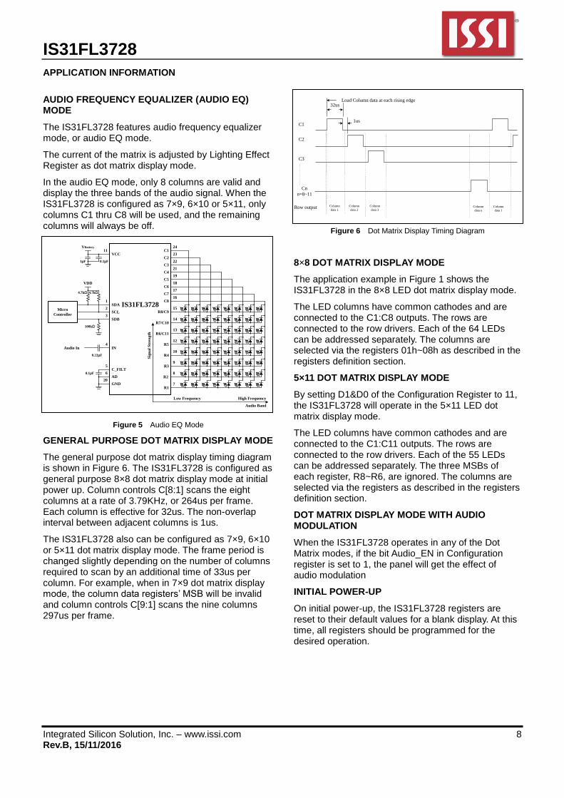
The general purpose dot matrix display timing diagram is shown in Figure 6. The IS31FL3728 is configured as general purpose 8×8 dot matrix display mode at initial power up. Column controls C[8:1] scans the eight columns at a rate of 3.79KHz, or 264us per frame. Each column is effective for 32us. The non-overlap interval between adjacent columns is 1us.
The IS31FL3728 also can be configured as 7×9, 6×10 or 5×11 dot matrix display mode. The frame period is changed slightly depending on the number of columns required to scan by an additional time of 33us per column. For example, when in 7×9 dot matrix display mode, the column data registers’ MSB will be invalid and column controls C[9:1] scans the nine columns 297us per frame.
C1
C2
C3
Cn
n=8~11
32us
1us
Load Column data at each rising edge
Column
data 1
Column
data 2
Column
data 3Column
data nRow output Column
data 1
Figure 6 Dot Matrix Display Timing Diagram
8×8 DOT MATRIX DISPLAY MODE
The application example in Figure 1 shows the IS31FL3728 in the 8×8 LED dot matrix display mode.
The LED columns have common cathodes and are connected to the C1:C8 outputs. The rows are connected to the row drivers. Each of the 64 LEDs can be addressed separately. The columns are selected via the registers 01h~08h as described in the registers definition section.
5×11 DOT MATRIX DISPLAY MODE
By setting D1&D0 of the Configuration Register to 11, the IS31FL3728 will operate in the 5×11 LED dot matrix display mode.
The LED columns have common cathodes and are connected to the C1:C11 outputs. The rows are connected to the row drivers. Each of the 55 LEDs can be addressed separately. The three MSBs of each register, R8~R6, are ignored. The columns are selected via the registers as described in the registers definition section.
DOT MATRIX DISPLAY MODE WITH AUDIO MODULATION
When the IS31FL3728 operates in any of the Dot Matrix modes, if the bit Audio_EN in Configuration register is set to 1, the panel will get the effect of audio modulation
INITIAL POWER-UP
On initial power-up, the IS31FL3728 registers are reset to their default values for a blank display. At this time, all registers should be programmed for the desired operation.

IS31FL3728
Integrated Silicon Solution, Inc. – www.issi.com 9 Rev.B, 15/11/2016
SOFTWARE SHUTDOWN MODE
The IS31FL3728 devices feature a software shutdown mode, wherein they consume only 1.7μA (typ.) current. Shutdown mode is entered via a write to the Configuration Register. When the IS31FL3728 is in shutdown mode, all current sources and digital drivers are switched off, so that the array is blanked.
Shutdown mode can either be used as a means of reducing power consumption or generating a flashing display (repeatedly entering and leaving shutdown mode).
Note: During shutdown mode all registers retain their data.

IS31FL3728
Integrated Silicon Solution, Inc. – www.issi.com 10 Rev.B, 15/11/2016
CLASSIFICATION REFLOW PROFILES
Profile Feature Pb-Free Assembly
Preheat & Soak Temperature min (Tsmin) Temperature max (Tsmax) Time (Tsmin to Tsmax) (ts)
150°C 200°C 60-120 seconds
Average ramp-up rate (Tsmax to Tp) 3°C/second max.
Liquidous temperature (TL) Time at liquidous (tL)
217°C 60-150 seconds
Peak package body temperature (Tp)* Max 260°C
Time (tp)** within 5°C of the specified classification temperature (Tc)
Max 30 seconds
Average ramp-down rate (Tp to Tsmax) 6°C/second max.
Time 25°C to peak temperature 8 minutes max.
Figure 7 Classification Profile

IS31FL3728
Integrated Silicon Solution, Inc. – www.issi.com 11 Rev.B, 15/11/2016
PACKAGE INFORMATION
QFN-24
Note: All dimensions in millimeters unless otherwise stated.

IS31FL3728
Integrated Silicon Solution, Inc. – www.issi.com 12 Rev.B, 15/11/2016
RECOMMENDED LAND PATTERN
QFN-24
0.5
0.85
0.3
4.8
2.8
Note:
1. Land pattern complies to IPC-7351.
2. All dimensions in MM.
3. This document (including dimensions, notes & specs) is a recommendation based on typical circuit board manufacturing parameters. Since land pattern design depends on many factors unknown (eg. user’s board manufacturing specs), user must determine suitability for use.

IS31FL3728
Integrated Silicon Solution, Inc. – www.issi.com 13 Rev.B, 15/11/2016
REVISION HISTORY
Revision Detail Information Date
A Initial release 2011.12.19
B
1. Add S3 temperature parameters.
2. Add ESD (HBM/CDM) value and θJA.
3. Update POD.
4. Add Land pattern.
5. Deleted tape and reel information.
6. IOUT test condition changes from VIN = 1.0Vp-p to VIN = 1.5Vp-p.
7. ISD Typ. changes from 0.2 to 1.7.
8. ISD Max. changes from 1.0 to 5.0.
2016.11.15