Atomically Thin Group V Elemental Films: Theoretical ... · Atomically Thin Group V Elemental...
7
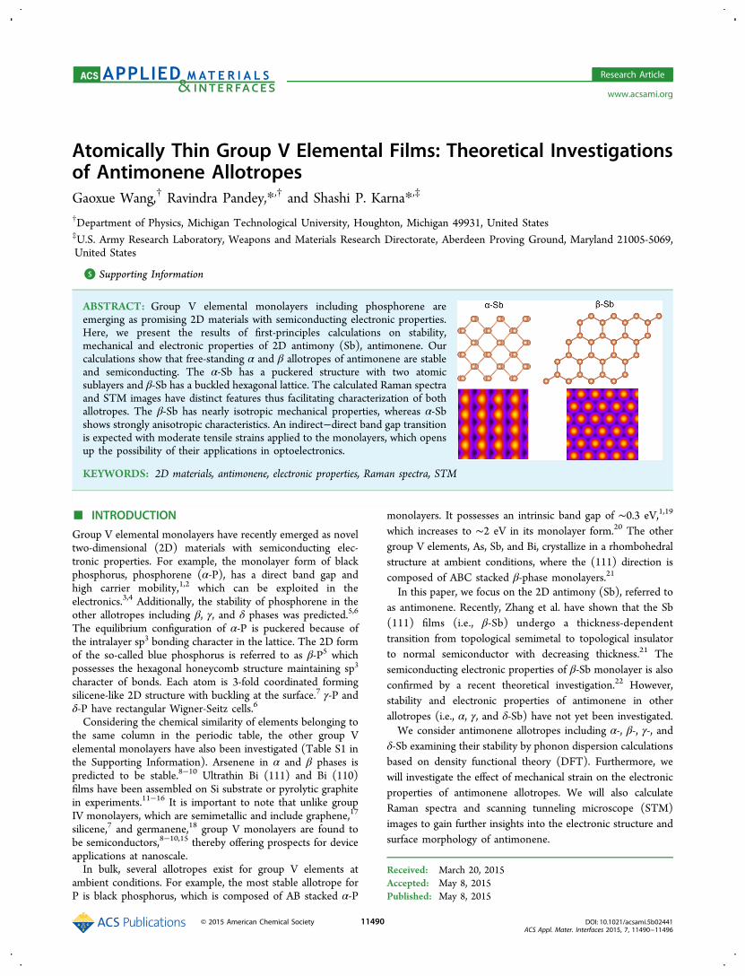
Atomically Thin Group V Elemental Films: Theoretical Investigations of Antimonene Allotropes Gaoxue Wang, † Ravindra Pandey,* ,† and Shashi P. Karna* ,‡ † Department of Physics, Michigan Technological University, Houghton, Michigan 49931, United States ‡ U.S. Army Research Laboratory, Weapons and Materials Research Directorate, Aberdeen Proving Ground, Maryland 21005-5069, United States * S Supporting Information ABSTRACT: Group V elemental monolayers including phosphorene are emerging as promising 2D materials with semiconducting electronic properties. Here, we present the results of first-principles calculations on stability, mechanical and electronic properties of 2D antimony (Sb), antimonene. Our calculations show that free-standing α and β allotropes of antimonene are stable and semiconducting. The α-Sb has a puckered structure with two atomic sublayers and β-Sb has a buckled hexagonal lattice. The calculated Raman spectra and STM images have distinct features thus facilitating characterization of both allotropes. The β-Sb has nearly isotropic mechanical properties, whereas α-Sb shows strongly anisotropic characteristics. An indirect−direct band gap transition is expected with moderate tensile strains applied to the monolayers, which opens up the possibility of their applications in optoelectronics. KEYWORDS: 2D materials, antimonene, electronic properties, Raman spectra, STM ■ INTRODUCTION Group V elemental monolayers have recently emerged as novel two-dimensional (2D) materials with semiconducting elec- tronic properties. For example, the monolayer form of black phosphorus, phosphorene (α-P), has a direct band gap and high carrier mobility, 1,2 which can be exploited in the electronics. 3,4 Additionally, the stability of phosphorene in the other allotropes including β, γ, and δ phases was predicted. 5,6 The equilibrium configuration of α-P is puckered because of the intralayer sp 3 bonding character in the lattice. The 2D form of the so-called blue phosphorus is referred to as β-P 5 which possesses the hexagonal honeycomb structure maintaining sp 3 character of bonds. Each atom is 3-fold coordinated forming silicene-like 2D structure with buckling at the surface. 7 γ-P and δ-P have rectangular Wigner-Seitz cells. 6 Considering the chemical similarity of elements belonging to the same column in the periodic table, the other group V elemental monolayers have also been investigated (Table S1 in the Supporting Information). Arsenene in α and β phases is predicted to be stable. 8−10 Ultrathin Bi (111) and Bi (110) films have been assembled on Si substrate or pyrolytic graphite in experiments. 11−16 It is important to note that unlike group IV monolayers, which are semimetallic and include graphene, 17 silicene, 7 and germanene, 18 group V monolayers are found to be semiconductors, 8−10,15 thereby offering prospects for device applications at nanoscale. In bulk, several allotropes exist for group V elements at ambient conditions. For example, the most stable allotrope for P is black phosphorus, which is composed of AB stacked α-P monolayers. It possesses an intrinsic band gap of ∼0.3 eV, 1,19 which increases to ∼2 eV in its monolayer form. 20 The other group V elements, As, Sb, and Bi, crystallize in a rhombohedral structure at ambient conditions, where the (111) direction is composed of ABC stacked β-phase monolayers. 21 In this paper, we focus on the 2D antimony (Sb), referred to as antimonene. Recently, Zhang et al. have shown that the Sb (111) films (i.e., β-Sb) undergo a thickness-dependent transition from topological semimetal to topological insulator to normal semiconductor with decreasing thickness. 21 The semiconducting electronic properties of β-Sb monolayer is also confirmed by a recent theoretical investigation. 22 However, stability and electronic properties of antimonene in other allotropes (i.e., α, γ, and δ-Sb) have not yet been investigated. We consider antimonene allotropes including α-, β-, γ-, and δ-Sb examining their stability by phonon dispersion calculations based on density functional theory (DFT). Furthermore, we will investigate the effect of mechanical strain on the electronic properties of antimonene allotropes. We will also calculate Raman spectra and scanning tunneling microscope (STM) images to gain further insights into the electronic structure and surface morphology of antimonene. Received: March 20, 2015 Accepted: May 8, 2015 Published: May 8, 2015 Research Article www.acsami.org © 2015 American Chemical Society 11490 DOI: 10.1021/acsami.5b02441 ACS Appl. Mater. Interfaces 2015, 7, 11490−11496
Transcript of Atomically Thin Group V Elemental Films: Theoretical ... · Atomically Thin Group V Elemental...
Atomically Thin Group V Elemental Films: Theoretical Investigationsof Antimonene AllotropesGaoxue Wang,† Ravindra Pandey,*,† and Shashi P. Karna*,‡
†Department of Physics, Michigan Technological University, Houghton, Michigan 49931, United States‡U.S. Army Research Laboratory, Weapons and Materials Research Directorate, Aberdeen Proving Ground, Maryland 21005-5069,United States
*S Supporting Information
ABSTRACT: Group V elemental monolayers including phosphorene areemerging as promising 2D materials with semiconducting electronic properties.Here, we present the results of first-principles calculations on stability,mechanical and electronic properties of 2D antimony (Sb), antimonene. Ourcalculations show that free-standing α and β allotropes of antimonene are stableand semiconducting. The α-Sb has a puckered structure with two atomicsublayers and β-Sb has a buckled hexagonal lattice. The calculated Raman spectraand STM images have distinct features thus facilitating characterization of bothallotropes. The β-Sb has nearly isotropic mechanical properties, whereas α-Sbshows strongly anisotropic characteristics. An indirect−direct band gap transitionis expected with moderate tensile strains applied to the monolayers, which opensup the possibility of their applications in optoelectronics.
KEYWORDS: 2D materials, antimonene, electronic properties, Raman spectra, STM
■ INTRODUCTION
Group V elemental monolayers have recently emerged as noveltwo-dimensional (2D) materials with semiconducting elec-tronic properties. For example, the monolayer form of blackphosphorus, phosphorene (α-P), has a direct band gap andhigh carrier mobility,1,2 which can be exploited in theelectronics.3,4 Additionally, the stability of phosphorene in theother allotropes including β, γ, and δ phases was predicted.5,6
The equilibrium configuration of α-P is puckered because ofthe intralayer sp3 bonding character in the lattice. The 2D formof the so-called blue phosphorus is referred to as β-P5 whichpossesses the hexagonal honeycomb structure maintaining sp3
character of bonds. Each atom is 3-fold coordinated formingsilicene-like 2D structure with buckling at the surface.7 γ-P andδ-P have rectangular Wigner-Seitz cells.6
Considering the chemical similarity of elements belonging tothe same column in the periodic table, the other group Velemental monolayers have also been investigated (Table S1 inthe Supporting Information). Arsenene in α and β phases ispredicted to be stable.8−10 Ultrathin Bi (111) and Bi (110)films have been assembled on Si substrate or pyrolytic graphitein experiments.11−16 It is important to note that unlike groupIV monolayers, which are semimetallic and include graphene,17
silicene,7 and germanene,18 group V monolayers are found tobe semiconductors,8−10,15 thereby offering prospects for deviceapplications at nanoscale.In bulk, several allotropes exist for group V elements at
ambient conditions. For example, the most stable allotrope forP is black phosphorus, which is composed of AB stacked α-P
monolayers. It possesses an intrinsic band gap of ∼0.3 eV,1,19
which increases to ∼2 eV in its monolayer form.20 The othergroup V elements, As, Sb, and Bi, crystallize in a rhombohedralstructure at ambient conditions, where the (111) direction iscomposed of ABC stacked β-phase monolayers.21
In this paper, we focus on the 2D antimony (Sb), referred toas antimonene. Recently, Zhang et al. have shown that the Sb(111) films (i.e., β-Sb) undergo a thickness-dependenttransition from topological semimetal to topological insulatorto normal semiconductor with decreasing thickness.21 Thesemiconducting electronic properties of β-Sb monolayer is alsoconfirmed by a recent theoretical investigation.22 However,stability and electronic properties of antimonene in otherallotropes (i.e., α, γ, and δ-Sb) have not yet been investigated.We consider antimonene allotropes including α-, β-, γ-, and
δ-Sb examining their stability by phonon dispersion calculationsbased on density functional theory (DFT). Furthermore, wewill investigate the effect of mechanical strain on the electronicproperties of antimonene allotropes. We will also calculateRaman spectra and scanning tunneling microscope (STM)images to gain further insights into the electronic structure andsurface morphology of antimonene.
Received: March 20, 2015Accepted: May 8, 2015Published: May 8, 2015
Research Article
www.acsami.org
© 2015 American Chemical Society 11490 DOI: 10.1021/acsami.5b02441ACS Appl. Mater. Interfaces 2015, 7, 11490−11496
■ COMPUTATIONAL DETAILSThe calculations were performed with the use of VASP programpackage.23 We employed the local density approximation (LDA)together with the projector-augmented-wave (PAW)24 method whichhas been shown to correctly describe Sb films.21 For bulk Sb, thecalculated lattice constant of 4.31 Å is in excellent agreement with theexperimental value of 4.30 Å25 giving confidence in the proposedapproach based on the LDA-DFT level of theory. To compare stabilityand structural parameters of different allotropes of antimonene, thePerdew−Burke−Ernzerhof (PBE)26 functional and the DFT-D2method of Grimme27 were also employed.In calculations, the energy convergence was set to 1 × 10⁻⁶ eV and
the residual force on each atom was smaller than 0.01 eV/Å. Thecutoff energy for the plane-wave basis was set to 500 eV. Thereciprocal space was sampled by a grid of (15 × 15 × 1) k points in theBrillouin zone. The vacuum distance normal to the plane was largerthan 20 Å to eliminate interaction between the replicas due to theperiod boundary conditions in the supercell approach of our model.The spin−orbit coupling (SOC) was included in calculations for theband structure. The Phonopy code28 was used for the phonondispersion calculation considering supercell of (4 × 5) for α-Sb, (5 ×5) for β-Sb, (5 × 4) for γ-Sb, and (3 × 3) for δ-Sb. The nonresonanceRaman spectra were obtained within density-functional perturbation
theory (DFPT) by second-order response to an electric field asimplemented in Quantum Espresso.29 The scanning tunnelingmicroscope (STM) images are based on BTH approximation,30
which has been successfully used to investigate tunneling character-istics of nanostructures including BN monolayer and phosphor-ene.31−34
■ RESULTS AND DISCUSSION
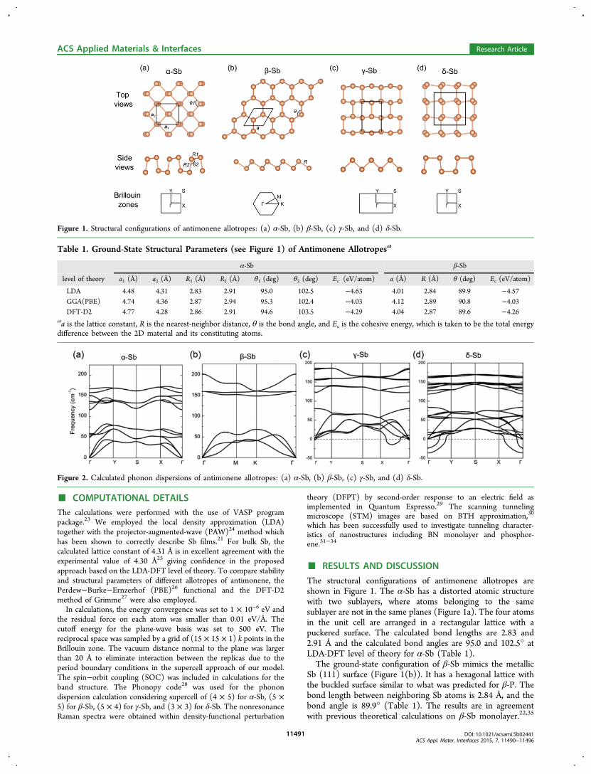
The structural configurations of antimonene allotropes areshown in Figure 1. The α-Sb has a distorted atomic structurewith two sublayers, where atoms belonging to the samesublayer are not in the same planes (Figure 1a). The four atomsin the unit cell are arranged in a rectangular lattice with apuckered surface. The calculated bond lengths are 2.83 and2.91 Å and the calculated bond angles are 95.0 and 102.5° atLDA-DFT level of theory for α-Sb (Table 1).The ground-state configuration of β-Sb mimics the metallic
Sb (111) surface (Figure 1(b)). It has a hexagonal lattice withthe buckled surface similar to what was predicted for β-P. Thebond length between neighboring Sb atoms is 2.84 Å, and thebond angle is 89.9° (Table 1). The results are in agreementwith previous theoretical calculations on β-Sb monolayer.22,35
Figure 1. Structural configurations of antimonene allotropes: (a) α-Sb, (b) β-Sb, (c) γ-Sb, and (d) δ-Sb.
Table 1. Ground-State Structural Parameters (see Figure 1) of Antimonene Allotropesa
α-Sb β-Sb
level of theory a1 (Å) a2 (Å) R1 (Å) R2 (Å) θ1 (deg) θ2 (deg) Ec (eV/atom) a (Å) R (Å) θ (deg) Ec (eV/atom)
LDA 4.48 4.31 2.83 2.91 95.0 102.5 −4.63 4.01 2.84 89.9 −4.57GGA(PBE) 4.74 4.36 2.87 2.94 95.3 102.4 −4.03 4.12 2.89 90.8 −4.03DFT-D2 4.77 4.28 2.86 2.91 94.6 103.5 −4.29 4.04 2.87 89.6 −4.26
aa is the lattice constant, R is the nearest-neighbor distance, θ is the bond angle, and Ec is the cohesive energy, which is taken to be the total energydifference between the 2D material and its constituting atoms.
Figure 2. Calculated phonon dispersions of antimonene allotropes: (a) α-Sb, (b) β-Sb, (c) γ-Sb, and (d) δ-Sb.
ACS Applied Materials & Interfaces Research Article
DOI: 10.1021/acsami.5b02441ACS Appl. Mater. Interfaces 2015, 7, 11490−11496
11491
Similar to γ- and δ-P,6 the γ- and δ-Sb have the rectangular unitcells, which are shown in Figures1c, d. The calculated bondlengths are (2.82 and 2.94 Å) and (2.87 and 2.93 Å) for γ-Sb,and δ-Sb, respectively.The stability of these antimonene allotropes is first
investigated by the calculation of the phonon dispersion curvesas shown in Figure 2. No imaginary vibrating mode is seen forα-Sb and β-Sb illustrating their stability as the free-standingmonolayers. The phonon dispersion curve of β-Sb is similar tothat of phosphorene with separated acoustic and optical modes.The maximum vibrational frequency in α-Sb and β-Sb is 170and 200 cm−1, respectively. Our calculations show that γ-Sb hasimaginary mode along Γ-X, and δ-Sb has imaginary modes at Γ.Employing a larger supercell model with a higher convergencecriteria also yielded imaginary frequencies for γ- and δ-Sb, thusconfirming their structural instabilities.The stability of α- and β-Sb monolayers is further examined
by the cohesive energy calculations using several exchange andcorrelational functional forms of DFT. As listed in Table 1, α-Sb has larger cohesive energy than β-Sb at the LDA-DFT (≈ 60meV) and DFT-D2 (≈ 30 meV) levels of theory, though bothmonolayers are nearly degenerate at GGA(PBE)-DFT level oftheory.The phonon free energy difference in the temperature range
of 0−600 K (Figure S1, Supporting Information) is calculatedto be less than 15 meV/atom between α-Sb and β-Sbsuggesting stabilization of both monolayers in experiments.Interestingly, a crossover in the cohesive energies of α-Sb andβ-Sb multilayers is predicted, which suggests that β-Sb is morestable than α-Sb in multilayers for thickness more than 3atomic layers (Figure S2, Supporting Information). Thethickness-dependent phase transition is mainly due to thestronger interlayer interaction in β multilayers (as will be shownlater), resulting into their stability over α-Sb multilayers. It maybe noticed that the experimental results on ultrathin Bi filmsshow stability of β-Bi over α-Bi for films with thickness morethan 4 atomic layers.15
Considering that the Raman measurements are generallyused to characterize 2D materials, such as graphene,36 we havecalculated the Raman spectra for α- and β-Sb monolayersshown in Figure 3. To assess the reliability of our approach, wefirst calculated the Raman spectrum of bulk Sb. Two Ramanpeaks, Eg at ∼100 cm−1 and A1g at ∼148 cm−1, were seen(Figure S3, Supporting Information) that are in agreement withexperiments.37 This gives confidence in our calculated LDA-DFT results for the Raman spectra of antimonene.α-Sb belongs to C2v group, and the modes, A1
1 at 63 cm−1, B1at 102 cm−1, A1
2 at 132 cm−1, and A13 at 147 cm−1, exhibit
prominent Raman scattering. A11 and A1
3 are out-of-planemodes. For the A1
1 mode, atoms belonging to the samesublayer vibrate along opposite directions. A1
3 is the mostdominating Raman peak for α-Sb for which atoms belonging tothe same sublayer vibrate along the same direction and the twosublayers vibrate opposite to each other. B1 and A1
2 are both in-plane modes in α-Sb. The β-Sb monolayer belongs to D3dgroup and the Raman active modes are at 150 cm−1 (Eg) and195 cm−1 (A1g). The Eg modes are doubly degenerate in-planemodes with two atoms in the unit cell vibrating along oppositedirections, and A1g is an out-of-plane vibrating mode.The calculated band structure, charge density and STM
images are shown in Figure 4. The α-Sb monolayer has arelatively small indirect band gap of ∼0.28 eV. The valenceband maximum (VBM) has a hybrid character of s orbitals and
in-plane px and py orbitals (Figure S4, Supporting Information),which shows an almost linear dispersion at VBM. Due to thepuckered structure, α-Sb has a stripelike STM surfacecharacteristic (Figure 4c). The electronic band structure(Figure 4d) for the β-Sb monolayer shows it to besemiconducting with an indirect band gap of ∼0.76 eV. Adotlike feature in the simulated STM image (Figure 4f) of theβ-Sb monolayer results from its buckled surface.Figure 5 shows atomic arrangements of antimonene
multilayers. β-Sb multilayers prefers an ABC stacking similarto bulk Sb (Figure 5d); the AA-stacked bilayer is higher inenergy by ∼24 meV/atom than the AB-stacked bilayer. Thecalculated interlayer distance is 3.65 Å. The band gaps of thebilayer and trilayer β-Sb (Figures S4 and S5, SupportingInformation) decrease significantly because of the small surfacestates splitting, as also predicted in the previous theoreticalreport on ultrathin β-Sb.21 It is interesting to note that thebinding energy of β-Sb bilayer is 124 meV/atom, which is muchlarger than that of other vdW layered materials, such as graphite(≈ 20 meV/atom38) and MoS2 (≈ 60 meV/atom38). This isdue to the partially overlapping of lone pair orbitals from theneighboring layers as seen from the charge density and thedeformation change density plots given in Figures 5e,f.Therefore, the mechanical exfoliation of bulk Sb is not expectedto be relatively easier than that of graphite or MoS2.α-Sb multilayers prefer AB stacking similar to that of black
phosphorus (Figure 5a). The interlayer distance in α-Sb bilayeris calculated to be 6.16 Å. The binding energy of the AB-stacked α-Sb bilayer is calculated to be 68 meV/atom, which isclose to those of other layered materials, e.g., MoS2.
38 Thecharge density in the interlayer region is very small (Figure 5b),and the electron redistribution in α-Sb bilayer (Figure 5c) is
Figure 3. (a) Calculated Raman spectra and (b, c) the correspondingvibrational modes of antimonene allotropes.
ACS Applied Materials & Interfaces Research Article
DOI: 10.1021/acsami.5b02441ACS Appl. Mater. Interfaces 2015, 7, 11490−11496
11492
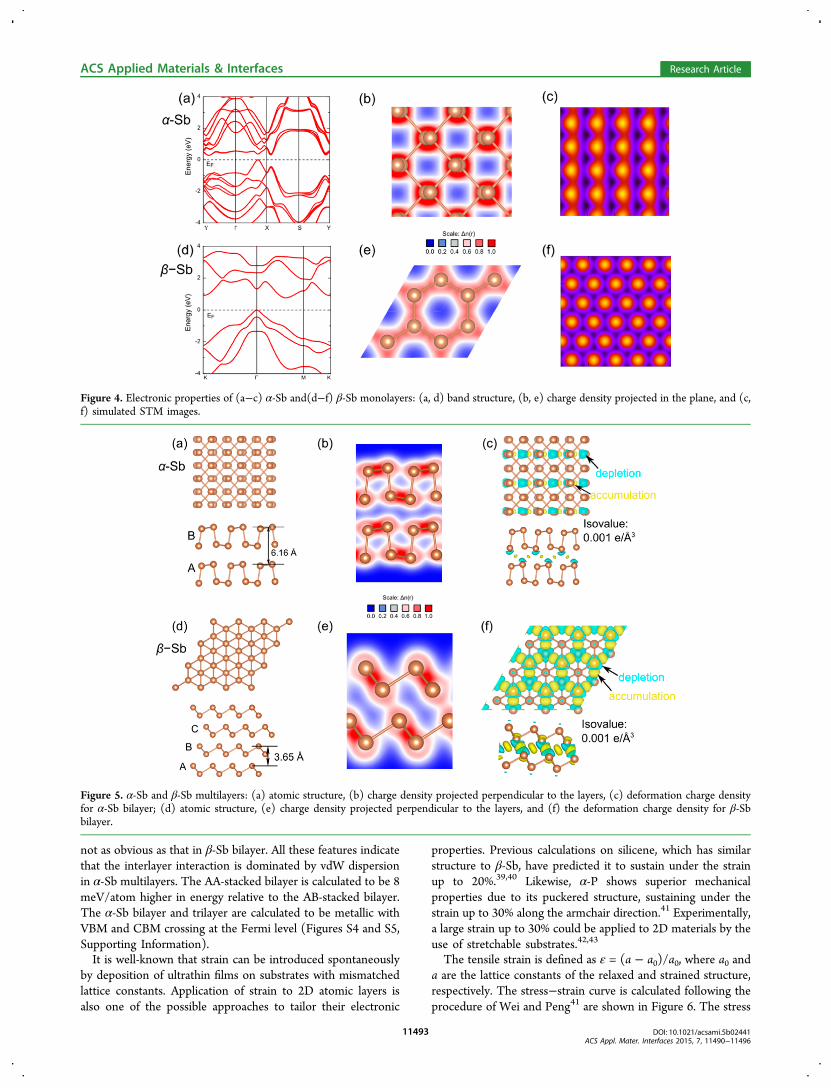
not as obvious as that in β-Sb bilayer. All these features indicatethat the interlayer interaction is dominated by vdW dispersionin α-Sb multilayers. The AA-stacked bilayer is calculated to be 8meV/atom higher in energy relative to the AB-stacked bilayer.The α-Sb bilayer and trilayer are calculated to be metallic withVBM and CBM crossing at the Fermi level (Figures S4 and S5,Supporting Information).It is well-known that strain can be introduced spontaneously
by deposition of ultrathin films on substrates with mismatchedlattice constants. Application of strain to 2D atomic layers isalso one of the possible approaches to tailor their electronic
properties. Previous calculations on silicene, which has similarstructure to β-Sb, have predicted it to sustain under the strainup to 20%.39,40 Likewise, α-P shows superior mechanicalproperties due to its puckered structure, sustaining under thestrain up to 30% along the armchair direction.41 Experimentally,a large strain up to 30% could be applied to 2D materials by theuse of stretchable substrates.42,43
The tensile strain is defined as ε = (a − a0)/a0, where a0 anda are the lattice constants of the relaxed and strained structure,respectively. The stress−strain curve is calculated following theprocedure of Wei and Peng41 are shown in Figure 6. The stress
Figure 4. Electronic properties of (a−c) α-Sb and(d−f) β-Sb monolayers: (a, d) band structure, (b, e) charge density projected in the plane, and (c,f) simulated STM images.
Figure 5. α-Sb and β-Sb multilayers: (a) atomic structure, (b) charge density projected perpendicular to the layers, (c) deformation charge densityfor α-Sb bilayer; (d) atomic structure, (e) charge density projected perpendicular to the layers, and (f) the deformation charge density for β-Sbbilayer.
ACS Applied Materials & Interfaces Research Article
DOI: 10.1021/acsami.5b02441ACS Appl. Mater. Interfaces 2015, 7, 11490−11496
11493
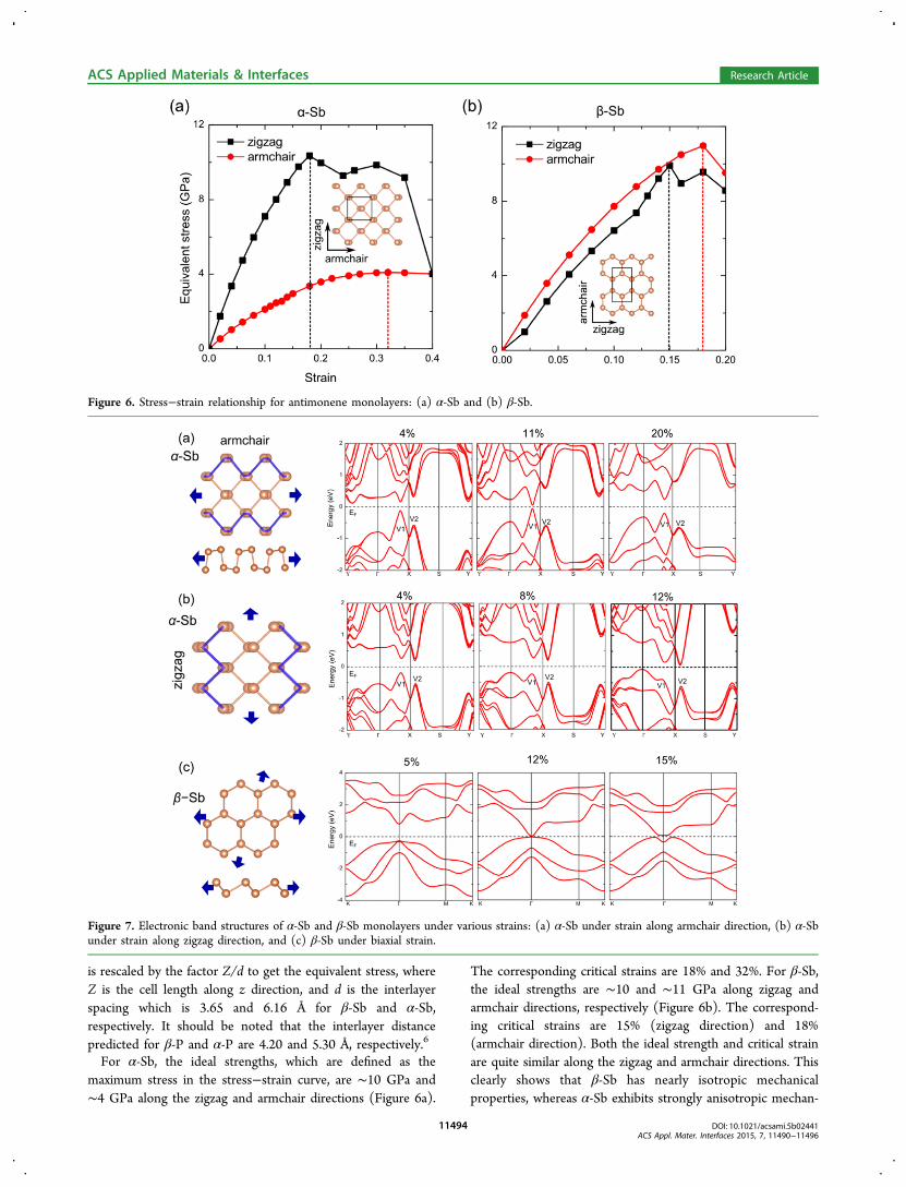
is rescaled by the factor Z/d to get the equivalent stress, whereZ is the cell length along z direction, and d is the interlayerspacing which is 3.65 and 6.16 Å for β-Sb and α-Sb,respectively. It should be noted that the interlayer distancepredicted for β-P and α-P are 4.20 and 5.30 Å, respectively.6
For α-Sb, the ideal strengths, which are defined as themaximum stress in the stress−strain curve, are ∼10 GPa and∼4 GPa along the zigzag and armchair directions (Figure 6a).
The corresponding critical strains are 18% and 32%. For β-Sb,the ideal strengths are ∼10 and ∼11 GPa along zigzag andarmchair directions, respectively (Figure 6b). The correspond-ing critical strains are 15% (zigzag direction) and 18%(armchair direction). Both the ideal strength and critical strainare quite similar along the zigzag and armchair directions. Thisclearly shows that β-Sb has nearly isotropic mechanicalproperties, whereas α-Sb exhibits strongly anisotropic mechan-
Figure 6. Stress−strain relationship for antimonene monolayers: (a) α-Sb and (b) β-Sb.
Figure 7. Electronic band structures of α-Sb and β-Sb monolayers under various strains: (a) α-Sb under strain along armchair direction, (b) α-Sbunder strain along zigzag direction, and (c) β-Sb under biaxial strain.
ACS Applied Materials & Interfaces Research Article
DOI: 10.1021/acsami.5b02441ACS Appl. Mater. Interfaces 2015, 7, 11490−11496
11494
ical characteristics. The critical strain along the armchairdirection is extremely large in α-Sb, which will lead to strainengineering of its electronic properties.Next, we examine the tensile strain effect on the electronic
properties of both Sb monolayers within the critical strainregion. α-Sb has an indirect band gap and the tensile strainalong the armchair direction induces an indirect−direct bandgap transition (Figure 7a). With strain larger than 6%, a directband gap at V1 is predicted. For 11% strain, the band gap at V1decreases to 0.05 eV. Thereafter, the band gap graduallyincreases with strain larger than 11%, and reaches to 0.45 eV at20% strain. For the tensile strain along zigzag direction (Figure7b), CBM moves to V2 point, and VBM moving to Γ for 8%strain. The strain induced indirect−direct band transition ismainly due to competition of states at Γ, V1 and V2. Similartheoretical results have also been reported for α-P44 and α-Aslayers.8
Because the β-Sb monolayer shows isotropic mechanicalproperties along the zigzag and armchair directions, a biaxialtensile strain was applied to the lattice as shown in Figure 7c. β-Sb monolayer has (minimum) indirect band gap of 0.76 eV atthe equilibrium configuration. Under 5% strain, its band gapbecomes direct at Γ. The band gap closes under 12% strain, andreopens for strain 20%. Considering that β-Sb monolayer stillpreserves its buckled structure under 15% strain, its band gapcan be effectively tuned by the in-plane strain.Since the mechanical exfoliation (scotch tape) approach may
not be the ideal approach to make antimonene, the standardchemical techniques are likely to play a major role in thesynthesis of 2D antimonene system. For example, the ultrathinBi(111) and Bi(110) films have been assembled on Si or highlyordered pyrolytic graphite (HOPG) substrate by vapordeposition.16,45 In the following work, we have considered anantimonene/graphene system taking graphene as substrate. Theα-Sb/graphene system is simulated with a rectangular supercellof (4.5 Å × 17.1 Å), and β-Sb/graphene is simulated with aparallelogram supercell of (10.6 Å × 10.6 Å) as shown in FigureS6 (see the Supporting Information). The choice of relativelylarge supercell essentially minimizes the lattice mismatchbetween graphene and antimonene to be less than 5%.In the equilibrium configurations, the interlayer distance is
larger than 3.2 Å at the LDA-DFT level of theory. Theintraplanar (Sb−Sb) bond lengths are 2.82 and 2.86 Å in α-Sb/graphene, and 2.83 Å in β-Sb/graphene, which are similar tothe calculated bond lengths in the freestanding monolayer. Thecalculated binding energies of α- and β-Sb on graphenesubstrate are 16 meV/atom and 14 meV/atom, respectively.The binding energy is defined in terms of energy differencebetween the constituent monolayers and the antimonene/graphene system. From the projected band structures (FigureS6, Supporting Information), the nature of the band gap of β-Sb monolayer is maintained on the graphene substrate, and asmall charge transfer from α-Sb to graphene is calculated as alsosuggested by shifting of the Fermi level (Figure S6, SupportingInformation). The calculated results therefore suggest thatgraphene could possibly serve as a substrate for the epitaxialgrowth of antimonene allotropes.
■ SUMMARYIn summary, DFT calculations are performed on 2Dantimonene atomic layers. Our results show that α- and β-Sbmonolayers are stable. Both monolayers are semiconductorswith indirect band gap. β-Sb has nearly isotropic mechanical
properties whereas α-Sb exhibits strongly anisotropic mechan-ical characteristics. Moderate tensile strain would induceindirect to direct band gap transition in antimonene. Thecalculated Raman spectrum prominently shows in-plane andout of plane vibrating modes that can be used to characterizeantimonene monolayers.
■ ASSOCIATED CONTENT*S Supporting InformationFigure S1: Helmholtz free energy of phonon as a function oftemperature for α-Sb and β-Sb. Figure S2: Cohesive energy ofα-Sb and β-Sb multilayers calculated at the LDA-DFT level oftheory. Figure S3: Simulated Raman spectrum for bulk Sb.Figure S4: Density of states of multilayer antimonene: (a) α-Sb,and (b) β-Sb. Figure S5: Band structure of multilayerantimonene: (a) α-Sb, and (b) β-Sb. Figure S6: Structuraland electronic properties of antimonene deposited ongraphene: (a, b) α-Sb/graphene and (c, d) β-Sb/graphene.Table S1: Summary of the stability of group V elementarymonolayers. Table S2: The ground state structural parametersof α- and β-Sb layers. The Supporting Information is availablefree of charge on the ACS Publications website at DOI:10.1021/acsami.5b02441.
■ AUTHOR INFORMATIONCorresponding Authors*E-mail: [email protected].*E-mail: [email protected] authors declare no competing financial interest.
■ ACKNOWLEDGMENTSRAMA and Superior, high performance computing clusters atMichigan Technological University, were used in obtainingresults presented in this paper. Support from Dr. S. Gowtham isgratefully acknowledged. This research was partially supportedby the Army Research Office through Grant W911NF-14-2-0088.
■ REFERENCES(1) Takao, Y.; Asahina, H.; Morita, A. Electronic Structure of BlackPhosphorus in Tight Binding Approach. J. Phys. Soc. Jpn. 1981, 50,3362−3369.(2) Lu, W.; Nan, H.; Hong, J.; Chen, Y.; Zhu, C.; Liang, Z.; Ma, X.;Ni, Z.; Jin, C.; Zhang, Z. Plasma-assisted Fabrication of MonolayerPhosphorene and its Raman Characterization. Nano Res. 2014, 7,853−859.(3) Liu, H.; Neal, A. T.; Zhu, Z.; Luo, Z.; Xu, X.; Tomanek, D.; Ye, P.D. Phosphorene: An Unexplored 2D Semiconductor with a High HoleMobility. ACS Nano 2014, 8, 4033−4041.(4) Xia, F.; Wang, H.; Jia, Y. Rediscovering Black Phosphorus as anAnisotropic Layered Material for Optoelectronics and Electronics. Nat.Commun. 2014, 5, 4458.(5) Zhu, Z.; Tomanek, D. Semiconducting Layered Blue Phosphorus:A Computational Study. Phys. Rev. Lett. 2014, 112, 176802.(6) Guan, J.; Zhu, Z.; Tomanek, D. Phase Coexistence and Metal-Insulator Transition in Few-Layer Phosphorene: A ComputationalStudy. Phys. Rev. Lett. 2014, 113, 046804.(7) Vogt, P.; De Padova, P.; Quaresima, C.; Avila, J.; Frantzeskakis,E.; Asensio, M. C.; Resta, A.; Ealet, B.; Le Lay, G. Silicene: CompellingExperimental Evidence for Graphenelike Two-Dimensional Silicon.Phys. Rev. Lett. 2012, 108, 155501.(8) Kamal, C.; Ezawa, M. Arsenene: Two-dimensional Buckled andPuckered Honeycomb Arsenic Systems. Phys. Rev. B 2015, 91, 085423.
ACS Applied Materials & Interfaces Research Article
DOI: 10.1021/acsami.5b02441ACS Appl. Mater. Interfaces 2015, 7, 11490−11496
11495
(9) Zhu, Z.; Guan, J.; Tomanek, D. Strain-induced metal-semi-conductor transition in monolayers and bilayers of gray arsenic: Acomputational study. Phys. Rev. B 2015, 91, 161404.(10) Zhiya, Z.; Jiafeng, X.; Dezheng, Y.; Yuhua, W.; Mingsu, S.;Desheng, X. Manifestation of unexpected semiconducting propertiesin few-layer orthorhombic arsenene. Appl. Phys. Express 2015, 8,055201.(11) Jnawali, G.; Klein, C.; Wagner, T.; Hattab, H.; Zahl, P.; Acharya,D.; Sutter, P.; Lorke, A.; Horn-von Hoegen, M. Manipulation ofElectronic Transport in the Bi(111) Surface State. Phys. Rev. Lett.2012, 108, 266804.(12) Wang, D.; Chen, L.; Liu, H.; Wang, X. Electronic Structures andTopological Properties of Bi (111) Ultrathin Films. J. Phys. Soc. Jpn.2013, 82, 094712.(13) Hirahara, T.; Fukui, N.; Shirasawa, T.; Yamada, M.; Aitani, M.;Miyazaki, H.; Matsunami, M.; Kimura, S.; Takahashi, T.; Hasegawa, S.;Kobayashi, K. Atomic and Electronic Structure of Ultrathin Bi(111)Films Grown on Bi2Te3 Substrates: Evidence for a Strain-InducedTopological Phase Transition. Phys. Rev. Lett. 2012, 109, 227401.(14) Jnawali, G.; Hattab, H.; Bobisch, C. A.; Bernhart, A.; Zubkov, E.;Moller, R.; Horn-von Hoegen, M. Homoepitaxial growth of Bi (111).Phys. Rev. B 2008, 78, 035321.(15) Kokubo, I.; Yoshiike, Y.; Nakatsuji, K.; Hirayama, H. UltrathinBi (110) Films on Si (111) Substrates. Phys. Rev. B 2015, 91, 075429.(16) Lu, Y.; Xu, W.; Zeng, M.; Yao, G.; Shen, L.; Yang, M.; Luo, Z.;Pan, F.; Wu, K.; Das, T. Topological Properties Determined by AtomicBuckling in Self-Assembled Ultrathin Bi (110). Nano Lett. 2014, 15,80−87.(17) Novoselov, K.; Geim, A. K.; Morozov, S.; Jiang, D.; Katsnelson,M.; Grigorieva, I.; Dubonos, S.; Firsov, A. Two-dimensional gas ofmassless Dirac fermions in graphene. Nature 2005, 438, 197−200.(18) Davila, M.; Xian, L.; Cahangirov, S.; Rubio, A.; Le Lay, G.Germanene: a Novel Two-dimensional Germanium Allotrope akin toGraphene and Silicene. New J. Phys. 2014, 16, 095002.(19) Warschauer, D. Electrical and Optical Properties of CrystallineBlack Phosphorus. J. Appl. Phys. 1963, 34, 1853−1860.(20) Tran, V.; Soklaski, R.; Liang, Y.; Yang, L. Layer-controlled BandGap and Anisotropic Excitons in Few-layer Black Phosphorus. Phys.Rev. B 2014, 89, 235319.(21) Zhang, P.; Liu, Z.; Duan, W.; Liu, F.; Wu, J. Topological andElectronic Transitions in a Sb (111) Aanofilm: The Interplay BetweenQuantum Confinement and Surface Effect. Phys. Rev. B 2012, 85,201410.(22) Zhang, S.; Yan, Z.; Li, Y.; Chen, Z.; Zeng, H. Atomically ThinArsenene and Antimonene: Semimetal−Semiconductor and Indirect−Direct Band-Gap Transitions. Angew. Chem. 2015, 54, 3112−3115.(23) Kresse, G.; Furthmuller, J. Efficiency of Ab-initio Total EnergyCalculations for Metals and Semiconductors Using a Plane-wave Basisset. Comput. Mater. Sci. 1996, 6, 15−50.(24) Kresse, G.; Joubert, D. From Ultrasoft Pseudopotentials to theProjector Augmented-wave Method. Phys. Rev. B 1999, 59, 1758−1775.(25) Barrett, C.; Cucka, P.; Haefner, K. The Crystal Structure ofAntimony at 4.2, 78 and 298 Degrees K. Acta Crystallogr. 1963, 16,451−453.(26) Perdew, J. P.; Burke, K.; Ernzerhof, M. Generalized GradientApproximation Made Simple. Phys. Rev. Lett. 1996, 77, 3865−3868.(27) Grimme, S. Semiempirical GGA-type Density FunctionalConstructed with a Long-range Dispersion Correction. J. Comput.Chem. 2006, 27, 1787−1799.(28) Togo, A.; Oba, F.; Tanaka, I. First-principles Calculations of theFerroelastic Transition between Rutile-type and CaCl2-type SiO2 athigh pressures. Phys. Rev. B 2008, 78, 134106.(29) Lazzeri, M.; Mauri, F. First-Principles Calculation of VibrationalRaman Spectra in Large Systems: Signature of Small Rings inCrystalline SiO2. Phys. Rev. Lett. 2003, 90, 036401.(30) Tersoff, J.; Hamann, D. R. Theory and Application for theScanning Tunneling Microscope. Phys. Rev. Lett. 1983, 50 (25), 1998−2001.
(31) He, H.; Pandey, R.; Pati, R.; Karna, S. P. Spin-polarized electrontransport of a self-assembled organic monolayer on a Ni(111)substrate: An organic spin switch. Phys. Rev. B 2006, 73, 195311.(32) Gupta, S. K.; He, H.; Banyai, D.; Si, M.; Pandey, R.; Karna, S. P.Effect of Si doping on the electronic properties of BN monolayer.Nanoscale 2014, 6, 5526−5531.(33) Wang, G.; Pandey, R.; Karna, S. P. Phosphorene oxide: stabilityand electronic properties of a novel two-dimensional material.Nanoscale 2015, 7, 524−531.(34) Wang, G.; Pandey, R.; Karna, S. P. Effects of extrinsic pointdefects in phosphorene: B, C, N, O, and F adatoms. Appl. Phys. Lett.2015, 106, 173104.(35) Liang, J.; Cheng, L.; Zhang, J.; Liu, H. Topological PhaseTransition in Antimonene Induced by Biaxial Tensile Strain; CornellUniversity: Ithaca, NY, 2015; arXiv:1502.01610.(36) Ferrari, A. C. Raman Spectroscopy of Graphene and Graphite:Disorder, Electron−phonon Coupling, Doping and NonadiabaticEffects. Solid State Commun. 2007, 143, 47−57.(37) Wang, X.; Kunc, K.; Loa, I.; Schwarz, U.; Syassen, K. Effect ofPressure on the Raman Modes of Antimony. Phys. Rev. B 2006, 74,134305.(38) Rydberg, H.; Dion, M.; Jacobson, N.; Schroder, E.; Hyldgaard,P.; Simak, S. I.; Langreth, D. C.; Lundqvist, B. I. Van der WaalsDensity Functional for Layered Structures. Phys. Rev. Lett. 2003, 91,126402.(39) Topsakal, M.; Ciraci, S. Elastic and Plastic Deformation ofGraphene, Silicene, and Boron Nitride Honeycomb Nanoribbonsunder Uniaxial Tension: A First-principles Density-Functional Theorystudy. Phys. Rev. B 2010, 81, 024107.(40) Qin, R.; Wang, C.-H.; Zhu, W.; Zhang, Y. First-principlesCalculations of Mechanical and Electronic Properties of Silicene underStrain. AIP Adv. 2012, 2, 022159.(41) Wei, Q.; Peng, X. Superior Mechanical Flexibility ofPhosphorene and Few-layer Black Phosphorus. Appl. Phys. Lett.2014, 104, 251915.(42) Wang, G.; Si, M.; Kumar, A.; Pandey, R. Strain engineering ofDirac cones in graphyne. Appl. Phys. Lett. 2014, 104, 213107.(43) Kim, K. S.; Zhao, Y.; Jang, H.; Lee, S. Y.; Kim, J. M.; Kim, K. S.;Ahn, J.-H.; Kim, P.; Choi, J.-Y.; Hong, B. H. Large-scale patterngrowth of graphene films for stretchable transparent electrodes. Nature2009, 457, 706−710.(44) Peng, X.; Wei, Q.; Copple, A. Strain-engineered direct-indirectband gap transition and its mechanism in two-dimensionalphosphorene. Phys. Rev. B 2014, 90, 085402.(45) Scott, S. A.; Kral, M. V.; Brown, S. A. A crystallographicorientation transition and early stage growth characteristics of thin Bifilms on HOPG. Surf. Sci. 2005, 587, 175−184.
ACS Applied Materials & Interfaces Research Article
DOI: 10.1021/acsami.5b02441ACS Appl. Mater. Interfaces 2015, 7, 11490−11496
11496