Atomic and electronic structure of two- dimensional Mo(1-x ...
27
Xia et al Atomic and electronic structure of two- dimensional Mo (1-x) W x S 2 alloys Xue Xia 1§ , Siow Mean Loh 1§ , Jacob Viner 2 , Natalie C. Teutsch 1 , Abigail J. Graham 1 , Viktor Kandyba 3 , Alexei Barinov 3 , Ana M. Sanchez 1 , David C. Smith 2 , Nicholas D. M. Hine 1* , Neil R. Wilson 1* 1 Department of Physics, University of Warwick, Coventry, CV4 7AL, UK 2 School of Physics and Astronomy, University of Southampton, Southampton SO17 1BJ, UK 3 Elettra - Sincrotrone Trieste, S.C.p.A., Basovizza (TS), 34149, Italy § these authors contributed equally E-mail: [email protected], [email protected] Received xxxxxx Accepted for publication xxxxxx Published xxxxxx Abstract Alloying enables engineering of the electronic structure of semiconductors for optoelectronic applications. Due to their similar lattice parameters, the two-dimensional semiconducting transition metal dichalcogenides of the MoWSeS group (MX2 where M= Mo or W and X=S or Se) can be grown as high-quality materials with low defect concentrations. Here we investigate the atomic and electronic structure of Mo(1-x)WxS2 alloys using a combination of high-resolution experimental techniques and simulations. Analysis of the Mo and W atomic positions in these alloys, grown by chemical vapour transport, shows that they are randomly distributed, consistent with Monte Carlo simulations that use interaction energies determined from first-principles calculations. Electronic structure parameters are directly determined from angle resolved photoemission spectroscopy measurements. These show that the spin- orbit splitting at the valence band edge increases linearly with W content from MoS2 to WS2, in agreement with linear-scaling density functional theory (LS-DFT) predictions. The spin- orbit splitting at the conduction band edge is predicted to reduce to zero at intermediate compositions. Despite this, polarisation-resolved photoluminescence spectra on monolayer Mo0.5W0.5S2 show significant circular dichroism, indicating that spin-valley locking is retained. These results demonstrate that alloying is an important tool for controlling the electronic structure of MX2 for spintronic and valleytronic applications. Keywords: 2D semiconductor, alloy, angle resolved photoemission spectroscopy, linear scaling density functional theory 1. Introduction Semiconducting transition metal dichalcogenide monolayers, such as the MoWSeS group (MX2 where M= Mo or W and X=S or Se), are of great interest both for their practical applications and for the fundamental science that can be studied in them. 1 Much of the interest has focused on the optical properties of MX2: they exhibit a transition from indirect gap in bulk to direct gap in monolayers, and strong Coulomb interactions lead to high exciton binding energies 2 . In the monolayers, spin-orbit coupling (SOC) splits both the valence band maximum (VBM) and conduction band minimum (CBM) to give spin-polarised bands at the Brillouin zone corners. 3,4 This leads to spin-valley locking, 5–8 with the
Transcript of Atomic and electronic structure of two- dimensional Mo(1-x ...

Xia et al
Atomic and electronic structure of two-
dimensional Mo(1-x)WxS2 alloys
Xue Xia1§, Siow Mean Loh1§, Jacob Viner2, Natalie C. Teutsch1, Abigail J. Graham1,
Viktor Kandyba3, Alexei Barinov3, Ana M. Sanchez1, David C. Smith2, Nicholas D.
M. Hine1*, Neil R. Wilson1*
1 Department of Physics, University of Warwick, Coventry, CV4 7AL, UK 2 School of Physics and Astronomy, University of Southampton, Southampton SO17 1BJ, UK 3Elettra - Sincrotrone Trieste, S.C.p.A., Basovizza (TS), 34149, Italy
§ these authors contributed equally
E-mail: [email protected], [email protected]
Received xxxxxx
Accepted for publication xxxxxx
Published xxxxxx
Abstract
Alloying enables engineering of the electronic structure of semiconductors for optoelectronic
applications. Due to their similar lattice parameters, the two-dimensional semiconducting
transition metal dichalcogenides of the MoWSeS group (MX2 where M= Mo or W and X=S
or Se) can be grown as high-quality materials with low defect concentrations. Here we
investigate the atomic and electronic structure of Mo(1-x)WxS2 alloys using a combination of
high-resolution experimental techniques and simulations. Analysis of the Mo and W atomic
positions in these alloys, grown by chemical vapour transport, shows that they are randomly
distributed, consistent with Monte Carlo simulations that use interaction energies determined
from first-principles calculations. Electronic structure parameters are directly determined
from angle resolved photoemission spectroscopy measurements. These show that the spin-
orbit splitting at the valence band edge increases linearly with W content from MoS2 to WS2,
in agreement with linear-scaling density functional theory (LS-DFT) predictions. The spin-
orbit splitting at the conduction band edge is predicted to reduce to zero at intermediate
compositions. Despite this, polarisation-resolved photoluminescence spectra on monolayer
Mo0.5W0.5S2 show significant circular dichroism, indicating that spin-valley locking is
retained. These results demonstrate that alloying is an important tool for controlling the
electronic structure of MX2 for spintronic and valleytronic applications.
Keywords: 2D semiconductor, alloy, angle resolved photoemission spectroscopy, linear scaling density functional theory
1. Introduction
Semiconducting transition metal dichalcogenide
monolayers, such as the MoWSeS group (MX2 where M= Mo
or W and X=S or Se), are of great interest both for their
practical applications and for the fundamental science that can
be studied in them.1 Much of the interest has focused on the
optical properties of MX2: they exhibit a transition from
indirect gap in bulk to direct gap in monolayers, and strong
Coulomb interactions lead to high exciton binding energies2.
In the monolayers, spin-orbit coupling (SOC) splits both the
valence band maximum (VBM) and conduction band
minimum (CBM) to give spin-polarised bands at the Brillouin
zone corners.3,4 This leads to spin-valley locking, 5–8 with the
Xia et al
2
potential for optically generated spin-polarised currents, and
the resultant interest in valleytronics9 and spintronics10 in
these materials.
Band engineering through alloying has been essential to the
development of III-V semiconductors, giving control over
band parameters such as band gaps and band alignments,
leading to their application in commercial optoelectronics.
Following this, theoretical and experimental works have
shown that for MX2 alloying allows not only continuous
tuning of the band gap over a large range, from 1.55 to 1.99
eV,11–18 but also control over the magnitude of SOC in both
the conduction and valence band.13,14,19 Combined, these band
parameters have dramatic influences on the optical and
electrical properties of MX2. However, due to the difficulty in
accurately determining the single-particle electronic structure,
there is still uncertainty over how the electronic structure
changes with alloying. The high exciton binding energies
complicate the determination of electronic structure
parameters from conventional optical spectroscopy
measurements, such as photoluminescence (PL). This leaves
some outstanding questions: for example the SOC is predicted
to change linearly with composition, but inferring the SOC
from the energy difference between A and B excitons
suggested a non-linear bowing in Mo(1-x)WxSe2 monolayers.20
With the comparatively small difference in lattice
parameters, high-quality MoWSeS alloys are relatively easy
to synthesize, either through direct growth of monolayers by
chemical or physical vapour deposition11,17,19,21–23, or by
mechanical exfoliation of bulk alloy crystals grown by
chemical vapour transport.14,24–26 In such alloys, the local
atomic arrangement can play an important role in determining
the resultant properties of the material. Both atomically
random14,19,25 and ordered27–29 alloying have previously been
observed in transition metal dichalcogenide monolayers and
theoretical studies have suggested the possibility of order-
disorder phase transitions.30,31 Study of the ordered alloy
phases revealed sensitivity of the bandstructure at both the
VBM and the CBM to composition, but specifically also
sensitivity at the CBM to ordering.31
In this report we study exfoliated flakes of CVT grown
Mo1-xWxS2 alloys. By comparing quantitative analysis of the
atomic structure determined by scanning transmission
electron microscopy (STEM) to Monte Carlo simulations, we
reveal that the atomic arrangements are consistent with those
expected from thermodynamic considerations. Starting from
these atomic structure models, and using large unit cells to
avoid simulation artefacts, we apply linear scaling DFT to
predict electronic structure changes with alloying.
Comparison with angle-resolved photoemission spectroscopy
(ARPES) valence band measurements shows that the SOC at
the VBM does indeed scale linearly with stoichiometry (x).
The predictions indicate that at intermediate compositions the
SOC at the CBM should be less than the disorder potential in
the alloys. Despite this, polarisation-resolved
photoluminescence measurements of a Mo0.5W0.5S2
monolayer show that spin-valley locking is retained and hence
that such alloys have a promising future in spintronic
applications.
2. Methods
Crystal growth and exfoliation. Single crystals were
synthesised by chemical vapor transport (CVT) in a two-step
process.32 First, Mo (purity 99.9%, Sigma-Aldrich), W (purity
99.9%, Sigma-Aldrich) and S (purity 99.9%, Sigma-Aldrich)
element powders were mixed stoichiometrically into an
ampoule. The ampoule was pumped down to a pressure of
10-6 mbar and sealed. The mixture was heated to 1000 °C for
3 days to form Mo1-xWxS2 powder. In the second step, crystals
were grown from this powder. The synthesised compounds
were transferred to a new quartz ampoule with larger diameter
and mixed with the transport agent, I2 (10 mg cm-3 of the
ampoule volume). To keep the I2 stable, the ampoule was
evacuated to 10-6 mbar in ice and sealed. The ampoule was
placed into a three-zone furnace as shown in Supplementary
Material section 1 (SuppMat S1), the charge zone was kept at
1050 °C for 20 days with the growth zone at 950 °C. After
cooling to room temperature, the ampoule was opened in air
and single crystals were collected at the growth end as shown
in the schematic figure in SuppMat S1.
For PL measurements, the as-grown crystals were
mechanically exfoliated onto a Si/SiO2 wafer using scotch
tape. Prior to peeling off, the substrates were heated for a few
minutes on a hot plate at 130°C.33 Monolayer flakes were
identified by their optical contrast, by their Raman spectra,
and by their PL emission. PL and Raman spectra were
acquired at room temperature with a confocal
microspectrometer (Renishaw inVia Reflex Raman
microscopes) with 442 nm and 532 nm excitation.
Compositional analysis. Crystal composition was analysed by
a combination of X-ray photoelectron spectroscopy (XPS) and
energy dispersive X-ray analysis (EDX), further details are
given in SuppMat S2. EDX showed uniform composition
across individual crystals, indicating homogeneity at the
microscale. The compositions determined by XPS and EDX
were consistent with each other and with those measured from
analysis of the atomic resolution STEM images, indicating
homogeneity also at the nanoscale.
Atomic resolution imaging. Flakes were mechanically
exfoliated onto chemical vapour deposition (CVD) grown
graphene on copper 34, then a layer of CVD graphene was wet
transferred on top.35 The bottom layer of copper was etched
away using ammonia persulphate, the stack gently washed
with deionised water, and then the graphene encapsulated
Xia et al
3
Mo1-xWxS2 monolayer flakes were transferred to a
transmission electron microscopy (TEM) support grid. STEM
analysis was performed in a JEOL ARM200F TEM with
CEOS probe and image aberration correctors at 80 kV. The
annular dark-field (ADF) images were recorded at a probe
current of ~23 pA and a convergence semi-angle of ~25 mrad
using a JEOL annular field detector with an inner and outer
collection semi-angle of 45 and 180 mrad, respectively.36, 37
The scanning rate was typically 20 µs per pixel and each
image consists of 2048 × 2048 pixels.36
Determining the atom positions. Image analysis of the STEM
data was used to analyse the atomic configuration in the
alloys. Thresholding, based on integrated intensity within a
region centred on each atom, was applied to determine the
atomic identities and this was then verified visually. The
number of W-W pairs at nth-nearest-neighbour distances was
counted for n = 1 to 18, based on the positions of the W atoms
in the alloy. Next, the total number of transition metal-
transition metal pairs at each distance was counted. The
number of W-W pairs is divided by the product of the total
number of transition metal-transition metal pairs and the W
atom composition x.
Electronic structure measurements. Angle resolved
photoemission spectroscopy (ARPES) data were acquired at
the Spectromicroscopy beamline38 of the Elettra synchrotron,
using 27 eV photon illumination and a sample temperature of
around 100 K. Spectra were acquired from crystals which
were cleaved in UHV immediately before analysis. Three-
dimensional data sets of the photoemitted intensity as a
function of kinetic energy and emission angles were acquired
around the line in reciprocal space along the high symmetry
direction from �̅� to �̅�. From this, 2D energy-momentum slices
were extracted showing the dispersion from �̅� to �̅�. The
dispersion of the upper valence band was determined by fitting
the corresponding peaks in the energy distribution curves
(EDC) with Lorentz functions. The effective mass was found
by fitting a parabola to the resultant band dispersions around
�̅�.
Polarisation-resolved low-temperature photoluminescence
spectroscopy. The PL was excited using a CW dye laser with
a wavelength of 625 nm via a 50x 0.55 NA microscope
objective producing a 2 µm laser spot. The power incident on
the sample was kept below 100 µW. The measurements were
performed in backscattering geometry with the sample in
vacuum at 4 K. In order to ensure good circular polarisation
purity, a quarter wave plate (Thorlabs AQWP05M-600) was
placed just before the objective so that in the rest of the optical
system the input and output polarisations corresponded to
vertical and horizontal linear polarisations. The output
polarisation was determined using a linear polariser (Thorlabs
LPVIS100) and a half wave plate (AHWP05M-600) used to
ensure a constant input polarisation for the spectrometer. The
spectrometer used was a Princeton Instruments TriVista 555
with a liquid nitrogen cooled CCD. Measurements were
repeated on multiple areas of the sample.
Monte Carlo simulations. We model the equilibrium
distribution of the cations W and Mo using an Ising-like model
of nearest-neighbour interactions between pairs of cations on
a hexagonal lattice. The model comprises a single layer with
120×120 in-plane unit cells, a size corresponding to several
times the largest apparent feature size in the final distributions.
This was initialised to a random distribution constructed to
achieve the target concentration x. The growth process was
simulated by Monte Carlo sampling on proposed site swaps to
achieve an equilibrium of the system after 20000 cycles at a
temperature of 800 K. To parameterise the Monte Carlo
simulations, DFT calculations were performed on a selection
of models, as shown in SuppMat Figure S3(a), to determine
the optimal value of the interaction energy for a pair of W
atoms on adjacent lattice sites.39 To validate this, DFT
calculations were performed for a selection of atomic
configurations extracted from those observed in the
experimental STEM images (see SuppMat Figure S3(c-d)).
For illustration and comparison, Monte Carlo simulations
were also performed with interaction energies of -50, 0 and 50
meV.
Plane-wave DFT. For calculations of the optimized lattice
constants of the pure materials, MoS2 and WS2, the plane-
wave DFT package CASTEP was used.40 A cut-off energy of
424.5 eV and a 10×10×1 k-point grid were used, and the
generalized gradient approximation of Perdew, Burke and
Ernzerhof (PBE) was employed41. Since the resulting lattice
constants for MoS2 and WS2 are very similar (within 0.3%),
the same value, 3.18 Å, was subsequently used for both
materials, thereby neglecting the very small lattice mismatch.
CASTEP calculations were also used to provide the
interaction energies for pairs of W atoms for the Monte Carlo
parameterization, with commensurate adjustments of the k-
point grid to 3×3×1 and 1×1×1 as the supercell size increased
to 4×4×1 and 12×12×1 respectively.
Linear-scaling DFT. The ONETEP linear-scaling density
functional theory package42 was applied to simulate large
supercells with random alloy configurations. ONETEP uses a
representation of the single-particle density matrix in terms of
a minimal number of support functions denoted non-
orthogonal generalized Wannier functions (NGWFs). The
NGWFs are themselves represented in terms of a grid of psinc
functions43 (a systematic basis equivalent to plane waves),
which here use a cut-off energy of 1200 eV, and an NGWF
cut-off radius of 10a0. The PBE functional was used, with
projector-augmented wave (PAW)44,45 potentials from the
JTH library46. The electronic properties of different random
configurations of atomic structures were calculated within an
Xia et al
4
8×8×1 supercell model. Mo1-xWxS2 monolayer models were
created for various concentrations, x, with cation distributions
determined according to the procedures described below. A
separate geometry optimisation was performed for each
structure, with force tolerance of 0.1 eV/Å. Since the band
structures obtained from the disordered alloy supercell
calculations have a heavily-folded band structure that is not
directly comparable to the ARPES results, the effective band
structure was calculated in the primitive cell using the spectral
function unfolding method14, 47, the adaptation of which to the
NGWF representation is described in Ref 48.
Virtual crystal approximation (VCA) calculations.
Calculations were performed within the Virtual Crystal
Approximation49 with the Quantum Espresso code.50,51 PAW
datasets representing the W and Mo potentials mixed in the
appropriate ratio x were constructed using the ‘virtual’ tool
within the Quantum Espresso package. Spin-orbit coupling
was included using the treatment described by dal Corso.52–54
3. Results and Discussion
Mo1-xWxS2 alloy crystals were grown by chemical vapour
transport, as described in Methods, across the range from x =
0 to 1. Their compositions, determined by a combination of
XPS and EDX analysis (see Methods and SuppMat S2 for
further details), were found to be consistent within 3%
between crystals grown in the same batch, and across
individual crystals when averaged at the micrometre scale.
When exfoliated to monolayers, they exhibit room
temperature photoluminescence with peak emission frequency
varying nonlinearly from 1.85 eV at x = 0 to 1.98 eV at x = 1,
consistent with prior literature reports 14 (SuppMat S4).
3.1 Atomic structure
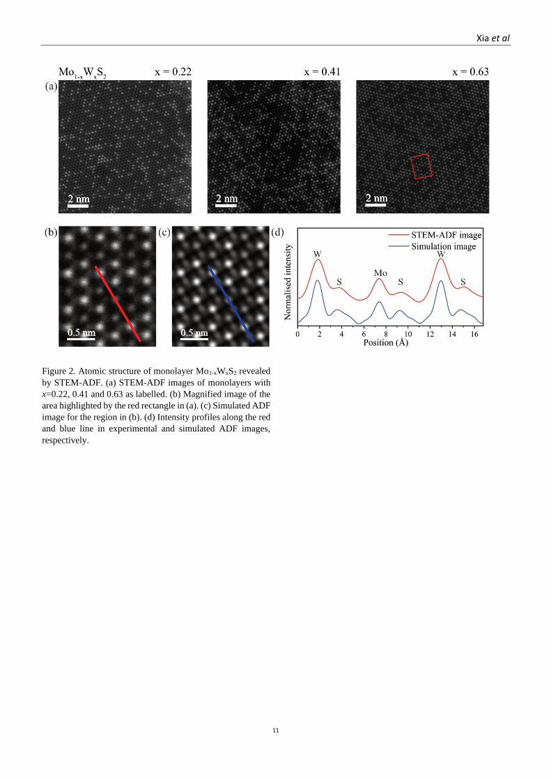
To determine whether the alloys are atomically ordered,
atomic resolution ADF-STEM images of monolayer Mo1-
xWxS2 flakes were acquired. Example images are given in
Figure 2a. In the magnified view, Figure 2b, the transition
metal atoms can be resolved but the chalcogen atoms give only
weak contrast, confirmed by the corresponding simulated
STEM image of the same area in Figure 2c. Due to the large
difference between their atomic numbers, there is also a clear
contrast difference between Mo (Z=42) and W (Z=74), again
verified by comparison between the line profiles of the
experimental and simulated images, as shown in Figure 2d.
For comparison, we performed Monte Carlo simulations
made with varying interaction energies, J, and compositions,
𝑥. Details of the simulation methodology are given in the
methods and SuppMat S3. To predict J for these alloys, a
range of atomic configurations were tested, from which the
binding energy of substitutional W atoms within the MoS2
monolayer was found to be well-represented by an average
value of J = 7.6 meV. This was further verified by comparison
of the Monte Carlo model to DFT calculations of a range of
larger cells (SuppMat S3). Figure 3a shows representative
atomic arrangements from Monte Carlo simulations,
comparing atomic arrangements for the predicted value of J =
7.6 meV to those with stronger interactions (J = ±50 meV) at
a simulation temperature of 800 K. At negative J, clusters of
W tend to form, while at positive J, isolated W atoms are
energetically preferred.
For J=0, when there is no energy difference between the W
and Mo, they are randomly arranged; qualitatively, Monte
Carlo simulations with J = 7.6 meV look similar to those with
J = 0. Although close visual inspection of the images can
suggest some ordering, quantitative statistical analysis is
required to rigorously test whether the Mo/W atoms are
randomly distributed within the sheets. SuppMat S3 shows
that in the Monte Carlo model, strong ordering disappears
beyond 50 K and is completely absent by temperatures
comparable to the growth conditions. For a given
composition, ADF-STEM images with areas of 120×120
atoms were analysed, fitting the intensity at each atom
coordinate and thresholding to determine the arrangement of
Mo and W atoms, as described in Methods. With the atom
coordinates identified, statistical analysis can be used to
investigate whether the arrangements are ordered. Following
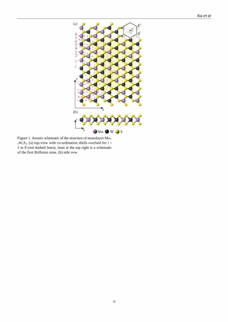
Cowley 55, we define the short range order parameter: 𝛼𝑖 =
1 − 𝑛𝑖 (𝑥 𝑐𝑖)⁄ , where 𝑛𝑖 is the number of W atoms out of the
𝑐𝑖 atoms in the ith coordination shell surrounding each W atom
(as defined schematically in Figure 1), and 𝑥 is the proportion
of W atoms (to (1 − 𝑥) Mo atoms) in the alloy.
Figure 3e shows the order parameters for Mo0.78W0.22S2
determined from the ADF-STEM images alongside those
calculated from analysis of the Monte Carlo simulations.
Order parameters for the other compositions followed similar
trends. For the simulated data, if J > 0 then 𝛼1 < 0, showing
a lower probability of finding a W atom neighbouring another
W atom. The magnitude of 𝛼𝑖 decreases rapidly with
increasing i, indicating a finite range to the order. If J < 0 then
𝛼1 > 0 (a tendency to cluster), and 𝛼𝑖 decreases
monotonically to 0 with increasing i. The order parameters
determined from the experimental data agree, within
uncertainties, with data from both J = 0 and J = 7.6 meV
simulations, consistent with a random distribution of W
atoms. We conclude that under the conditions used for the
growth of these crystals, the resultant atomic distributions are
indistinguishable from a random distribution and are
consistent with those expected at thermodynamic equilibrium
at the elevated growth temperature of this system.
3.2 Electronic structure
To correlate the electronic structure to the atomic structure,
the valence band dispersions of the Mo1-xWxS2 alloy crystals
were measured by ARPES. Since the measurements are
surface sensitive, the as-grown bulk crystals were mounted

Xia et al
5
flat onto a sample plate and cleaved in the ultrahigh vacuum
(UHV) chamber immediately prior to analysis, to generate the
clean surface required. Cleaving naturally results in exposure
of the (002) planes to the beam, so that ARPES probes the
electronic structure in the plane of the 2D layer.
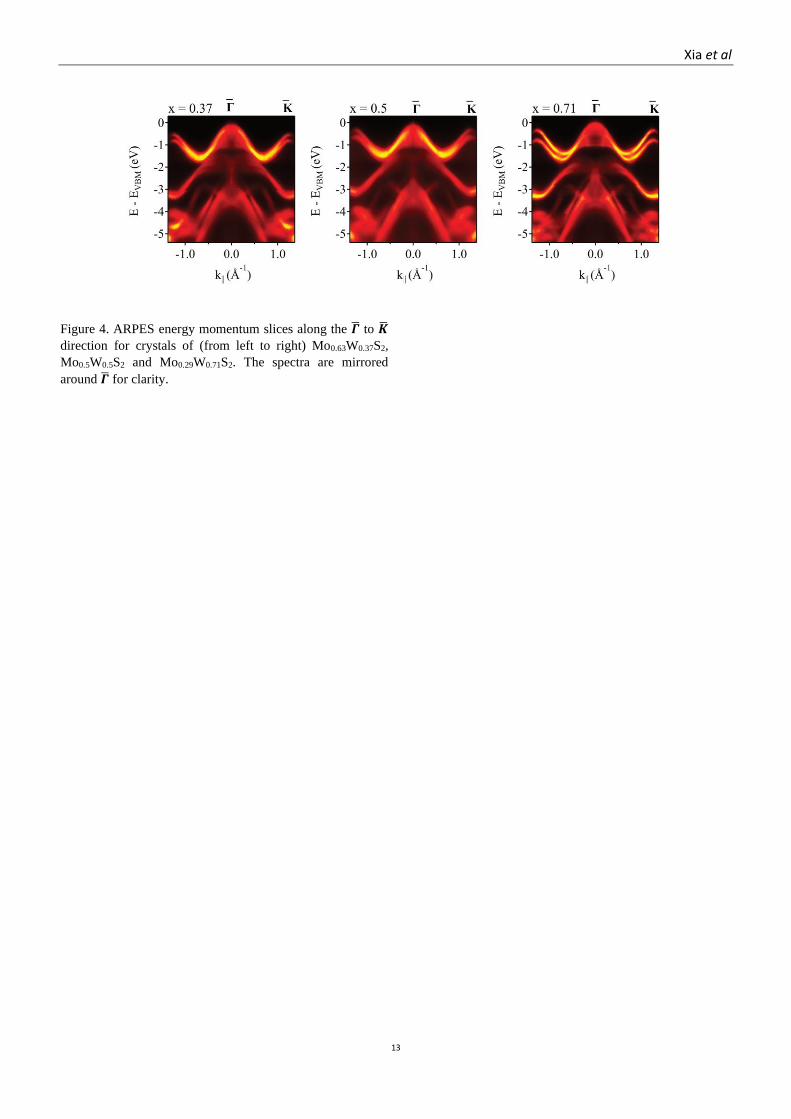
Typical spectra are given in Figure 4, showing the
dispersion from �̅� to �̅� for three alloy compositions:
Mo0.63W0.37S2, Mo0.5W0.5S2 and Mo0.29W0.71S2. We
concentrate our analysis on the structure around the zone
corners at K where, for the monolayers, the VBM is found.
Around K, the spin-split upper valence band has in-plane
orbital composition from the metal dx2-y2 +dxy and, to a lesser
extent, the chalcogen px+y.56 This results in a weak kz
dispersion such that the key features of the spectra in that
region are quantitatively similar for bulk and monolayer
materials.57, 58 From this dispersion, band parameters can be
determined such as the spin-orbit splitting of the bands at K,
the effective mass, and the band width (see the schematic in
Figure 5).
The qualitative trends are apparent by visual inspection of
the ARPES spectra: as the W content increases, the spin-orbit
splitting between the upper valence bands near K (SOCVB)
increases; the band width (Dvb) increases and the effective
mass decreases. To quantitatively evaluate the evolution of the
band structure with composition, measurements were
performed on all the compositions (x = 0.22, 0.37, 0.49, 0.71,
0.87 and 1) and band parameters extracted quantitatively by
fitting the ARPES spectra, as described in Methods. The data
are presented in Figure 6, and compared to first principles
calculations as described below.
Ab initio calculations of the electronic structure across the
alloy compositions were made using two approaches: the
virtual crystal approximation (VCA),49 where fractional atom
compositions are considered within the primitive cell of pure
materials; and the more computationally intensive approach of
calculating the electronic structure of large supercells with
varying ratios of Mo:W atoms. The details of each approach
are described in Methods and Supplementary Materials. In
brief, the Quantum Espresso package50,51 was used for the
VCA calculations, and linear-scaling density functional theory
(LS-DFT) calculations were performed on 8×8×1 supercells
(192 atoms) by the ONETEP package.59 The LS-DFT
calculations were unfolded into the primitive cell of the pure
monolayers 48; an example spectral function, for Mo0.5W0.5S2,
is shown in Figure 5, and spectral functions for the other
concentrations can be see in SuppMat Figure S7. Band
structure parameters were determined from fitting the spectral
functions.
Figure 6 compares the band structure parameters measured
from the experimental data to those calculated by LS-DFT and
VCA simulations, as a function of the W content in the alloy.
As the ARPES spectra probe the valence band, direct
experimental measurements of the conduction band edge and
band gap (Eg) are not possible from this data. Instead, the
predicted Eg are compared to the PL emission peak energy in
Figure 6a. DFT calculations normally underestimate Eg,6 so
we concentrate on the trends with composition. As previously
reported,14 the PL peak energy changes non-linearly with
composition, with the bowing parameter here determined to
be 0.17 ± 0.01 eV. This non-linear dependence of Eg on x is
expected due to the change in orbital characteristic of the
states at the conduction band edge from MoS2 to WS2.14 LS-
DFT predicts qualitatively similar changes in Eg, with a
bowing parameter of 0.12 ± 0.01 eV, but with a smaller change
in Eg (Eg = 1.63 eV for MoS2 and 1.62 eV for WS2) than
observed in the change in PL peak emission energy (1.85 eV
for MoS2 increasing to 1.98 eV for WS2). The magnitude of
Eg determined from VCA is similar to the LS-DFT
calculations, but the bowing parameter becomes negative (-
0.02 ± 0.01 eV), showing that the VCA predictions deviate
from the experimental observations.
Caution should be taken when comparing the PL emission
peak energies to the predicted band gaps (Eg) which are
determined from the energy difference between the VBM and
the CBM. The large exciton binding energy (several hundred
meV) means that the PL peak emission energy is not a good
measurement of the single-particle electronic band gap.2
Interpretation of the PL is further complicated by the change
in order of the spin-polarised conduction and valence bands,
as shown schematically in Figure 5b. The PL emission is from
the A exciton (bright exciton) in the K valley, corresponding
to an electron transition between states of the same spin. For x
= 0 (MoS2), this corresponds to the VBM and CBM states. But
at x = 1 (WS2), this has changed and the bright A exciton
emission comes from the second-lowest lying conduction
band which is greater in energy than the CBM by the spin-
orbit splitting at the conduction band edge (around 30 meV for
WS2).
Prior direct measurements of Eg from ARPES of
electrostatically doped monolayers found Eg = 2.07 ± 0.05 eV
for MoS2 and Eg = 2.03 ± 0.05 eV for WS2 60, only a small
change in band gap as also seen in the LS-DFT results. The
difference between the LS-DFT and PL data then suggests a
consistent decrease in exciton binding energy as the W content
increases.
ARPES provides a direct and visual measurement of the
valence band dispersion of the alloys, allowing easier
comparison to calculated spectra than is possible from optical
spectroscopy data. Measured values of SOCVB from the Mo1-
xWxS2 single crystals (blue data points) are compared in Figure
6b to those calculated for the monolayer alloys by LS-DFT
(black) and VCA (red). The measured value for WS2 (SOCVB
= 458 ± 10 meV) is consistent with prior reports for the bulk
crystals (450 ± 30 meV 39), and for a monolayer flake of WS2
(450 ± 30 meV 60). For the experimental results, SOCVB
increases linearly as a function of the W content, within the
Xia et al
6
error bars. The LS-DFT predictions show a similar linear
trend, with a systematic under-estimate of the experimental
results by around 50 meV. The VCA calculations of SOCVB
are similar in magnitude to the experimental measurements
but show a non-linear dependence on composition. A LS-DFT
simulation was also made using the atom positions determined
directly from a STEM image: the band parameters for this
simulation are shown as the purple data points in the graphs in
Figure 6 and are consistent with the other LS-DFT
simulations. The band width (Dvb), Figure 6c, follows similar
trends to SOCVB: the agreement between the experimental
data and the LS-DFT data is excellent, other than a systematic
offset (under-estimate) between the two; and the VCA data
shows a bowing that is not present in either the LS-DFT or
experimental data.
Figure 6d compares the evolution of the valence band
effective mass (around K and in the Γ to K direction)
calculated from ARPES spectra, the LS-DFT and VCA
calculations. It is difficult to accurately determine the effective
mass from the ARPES spectra, as a result the uncertainties are
large and there are no clear trends. From the DFT calculations
it is clear that the effective mass decreases monotonically with
x, consistent with the increasing curvature of the bands and
increasing band widths. This decrease in effective mass is also
consistent with a decrease in exciton binding energy with
increasing W content.
The ARPES spectra do not give information about the
conduction band as they only probe the occupied states.
However, the spin-orbit splitting at the conduction band edge
(SOCCB) can be extracted from the DFT spectral functions and
this is plotted as a function of composition in Figure 6e. It is
an order of magnitude lower than SOCVB. At small x, closer to
pure MoS2, the order of the conduction bands changes, see
Figure 5b. Hence SOCCB initially decreases to zero and then
increases with x. Although the LS-DFT and VCA calculations
do not quantitatively agree over the composition at which
SOCCB = 0, it is clear that at intermediate compositions SOCCB
is small. At x= 0 and x = 1, the small differences between the
results are due to the different approaches to SOC taken by the
two simulation packages: ONETEP uses a perturbative
approach to SOC, whereas Espresso uses a full SOC treatment
integrated into the self-consistency procedure.
Calculations were performed on three different random
realisations of the 8×8 supercells for each x, allowing a rough
estimate of the disorder potential to be made, on a similar
lengthscale to the exciton radius, based on the variation of the
CBM position between these random realisations. From these
we observe that the disorder potential is larger than SOCCB at
least for 0.125 ≤ x ≤ 0.5, becoming smaller again as SOCCB
increases (see SuppMat S5). This casts doubt over the usual
picture of separated states split by SOC at the conduction band
edge and merits further investigation of the spin-valley
locking in these alloys.61
3.3 Spin-valley locking
To test whether spin-valley locking is retained in the alloys,
optical spectroscopy measurements were performed on an
exfoliated heterostructure consisting of a monolayer flake of
Mo0.5W0.5S2 encapsulated in hBN. An optical image, and
schematic, of the sample is shown in Figure 7a. Polarisation-
resolved PL spectra, Figure 7b, show clear circular dichroism:
excitation with righthand circularly polarised light (σ+) leads
to emission of mainly σ+ light, whilst σ- excitation leads to σ-
emission. Excitation with vertical linear polarisation
(corresponding to (σ+ + σ−)/√2) results in emission with an
equal amount of σ+ and σ- circular components. The PL
spectra are plotted with normalised intensity to allow direct
comparison of the excitations with different polarisations. The
valley polarisation, η =𝑃𝐿(𝜎+)−𝑃𝐿(𝜎−)
𝑃𝐿(𝜎+)−𝑃𝐿(𝜎−) where PL(σ±) is the
intensity of the corresponding circularly polarised component
of the PL emission,9 is found to be η = 0.47 under σ+ excitation
and under σ- excitation. These results are fully consistent with
the expectations from the optical selection rules for the spin-
polarised monolayer materials and with previous observations
of spin-valley locking in pure monolayer MoWSeS flakes,5–8
showing that spin-valley locking is retained for the monolayer
alloys despite the atomic-scale heterogeneity in the alloys and
the small SOCCB.
4. Conclusions
No ordering or segregation was found in CVT grown
Mo1-xWxS2 alloys, consistent with Monte Carlo simulations
parameterised by ab initio calculations. ARPES measurements
showed that the spin orbit coupling at the valence band edge
increases linearly with increasing x (increasing W content).
LS-DFT simulations using large unit cells gave predictions
consistent with the ARPES measurements, but DFT
simulations using fractional atom concentrations in a primitive
unit cell were found to be inconsistent with the experimental
results. This conforms to expectations of the known severe
limitations of the predictive power of VCA, which becomes
even more apparent for properties that are nonlinear with
atomic number Z, such as SOC. This is especially apparent for
materials which retain some localised character in the valence
band, and strongly suggests instead the need for large-scale
disordered models to study alloy properties. From the LS-DFT
models, for intermediate alloy compositions the spin orbit
coupling is predicted to be smaller than the spatially localised
changes in the conduction band edge due to the atomic-scale
heterogeneity of the alloy. Despite this, polarisation-resolved
PL measurements of a monolayer Mo0.5W0.5S2 flake show
circular dichroism consistent with spin-valley locking. The
ability to rationally and continuously tune the spin-orbit
coupling, effective mass and band gap suggests a promising
Xia et al
7
future for MX2 alloys in valleytronic and spintronic
applications.
Acknowledgements
David Quigley is thanked for the provision of a Monte
Carlo model code which was adapted for the current work.
The Engineering and Physical Sciences Research Council
supported studentships for NCT (EP/M508184/1) and AJG
(EP/R513374/1), and funded NW and NDMH through
EP/P01139X/1. XXia and SML were supported by University
of Warwick Chancellor’s Scholarships. Computing resources
were provided by the High Performance Computing Service,
the Scientific Computing Research Technology Platform of
the University of Warwick, and the UK national high
performance computing service, ARCHER, via the UKCP
consortium (EP/P022561/1). The research leading to this
result has been supported by the project CALIPSOplus under
Grant Agreement 730872 from the EU Framework
Programme for Research and Innovation HORIZON 2020.
References
(1) Manzeli, S.; Ovchinnikov, D.; Pasquier, D.; Yazyev, O. V.;
Kis, A. 2D Transition Metal Dichalcogenides. Nat. Rev.
Mater. 2017, 2 (8), 17033.
https://doi.org/10.1038/natrevmats.2017.33.
(2) Wang, G.; Chernikov, A.; Glazov, M. M.; Heinz, T. F.;
Marie, X.; Amand, T.; Urbaszek, B. Colloquium : Excitons
in Atomically Thin Transition Metal Dichalcogenides. Rev.
Mod. Phys. 2018, 90 (2), 021001.
https://doi.org/10.1103/RevModPhys.90.021001.
(3) Liu, G.-B. Bin; Xiao, D.; Yao, Y.; Xu, X.; Yao, W.
Electronic Structures and Theoretical Modelling of Two-
Dimensional Group-VIB Transition Metal
Dichalcogenides. Chem. Soc. Rev. 2015, 44 (9), 2643–
2663. https://doi.org/10.1039/C4CS00301B.
(4) Kormányos, A.; Burkard, G.; Gmitra, M.; Fabian, J.;
Zólyomi, V.; Drummond, N. D.; Fal’ko, V.; Fal’ko, V. K ·
p Theory for Two-Dimensional Transition Metal
Dichalcogenide Semiconductors. 2D Mater. 2015, 2 (2),
022001. https://doi.org/10.1088/2053-1583/2/2/022001.
(5) Mak, K. F.; He, K.; Shan, J.; Heinz, T. F. Control of Valley
Polarization in Monolayer MoS 2 by Optical Helicity.
2012, 7 (June), 494–498.
https://doi.org/10.1038/nnano.2012.96.
(6) Cao, T.; Wang, G.; Han, W.; Ye, H.; Zhu, C.; Shi, J.; Niu,
Q.; Tan, P.; Wang, E.; Liu, B.; Feng, J. Valley-Selective
Circular Dichroism of Monolayer Molybdenum
Disulphide. Nat. Commun. 2012, 3 (1), 887.
https://doi.org/10.1038/ncomms1882.
(7) Zeng, H.; Dai, J.; Yao, W.; Xiao, D.; Cui, X. Valley
Polarization in MoS2 Monolayers by Optical Pumping.
Nat. Nanotechnol. 2012, 7 (8), 490–493.
https://doi.org/10.1038/nnano.2012.95.
(8) Aivazian, G.; Gong, Z.; Jones, A. M.; Chu, R.-L. L.; Yan,
J.; Mandrus, D. G.; Zhang, C.; Cobden, D.; Yao, W.; Xu,
X. D. Magnetic Control of Valley Pseudospin in
Monolayer WSe2. Nat. Phys. 2015, 1406 (2), 2546.
https://doi.org/10.1038/nphys3201.
(9) Schaibley, J. R.; Yu, H.; Clark, G.; Rivera, P.; Ross, J. S.;
Seyler, K. L.; Yao, W.; Xu, X. Valleytronics in 2D
Materials. Nat. Rev. Mater. 2016, 1 (11), 16055.
https://doi.org/10.1038/natrevmats.2016.55.
(10) Avsar, A.; Ochoa, H.; Guinea, F.; Ozyilmaz, B.; van
Wees, B. J.; Vera-Marun, I. J. Colloquium: Spintronics in
Graphene and Other Two-Dimensional Materials. 2019.
(11) Feng, Q.; Mao, N.; Wu, J.; Xu, H.; Wang, C.; Zhang, J.;
Xie, L. Growth of MoS 2(1– x ) Se 2 x ( x = 0.41–1.00)
Monolayer Alloys with Controlled Morphology by
Physical Vapor Deposition. ACS Nano 2015, 9 (7), 7450–
7455. https://doi.org/10.1021/acsnano.5b02506.
(12) Li, H.; Duan, X.; Wu, X.; Zhuang, X.; Zhou, H.; Zhang,
Q.; Zhu, X.; Hu, W.; Ren, P.; Guo, P.; Ma, L.; Fan, X.;
Wang, X.; Xu, J.; Pan, A.; Duan, X. Growth of Alloy MoS
2 x Se 2(1– x ) Nanosheets with Fully Tunable Chemical
Compositions and Optical Properties. J. Am. Chem. Soc.
2014, 136 (10), 3756–3759.
https://doi.org/10.1021/ja500069b.
(13) Xi, J.; Zhao, T.; Wang, D.; Shuai, Z. Tunable Electronic
Properties of Two-Dimensional Transition Metal
Dichalcogenide Alloys: A First-Principles Prediction. J.
Phys. Chem. Lett. 2014, 5 (2), 285–291.
https://doi.org/10.1021/jz402375s.
(14) Chen, Y.; Xi, J.; Dumcenco, D. O.; Liu, Z.; Suenaga, K.;
Wang, D.; Shuai, Z.; Huang, Y.-S. S.; Xie, L. Tunable
Band Gap Photoluminescence from Atomically Thin
Transition-Metal Dichalcogenide Alloys. ACS Nano 2013,
7 (5), 4610–4616. https://doi.org/10.1021/nn401420h.
(15) Feng, Q.; Zhu, Y.; Hong, J.; Zhang, M.; Duan, W.; Mao,
N.; Wu, J.; Xu, H.; Dong, F.; Lin, F.; Jin, C.; Wang, C.;
Zhang, J.; Xie, L. Growth of Large-Area 2D MoS 2(1- x )
Se 2 x Semiconductor Alloys. Adv. Mater. 2014, 26 (17),
2648–2653. https://doi.org/10.1002/adma.201306095.
(16) Kutana, A.; Penev, E. S.; Yakobson, B. I. Engineering
Electronic Properties of Layered Transition-Metal
Dichalcogenide Compounds through Alloying. Nanoscale
2014, 6 (11), 5820–5825.
https://doi.org/10.1039/c4nr00177j.
(17) Mann, J.; Ma, Q.; Odenthal, P. M.; Isarraraz, M.; Le, D.;
Preciado, E.; Barroso, D.; Yamaguchi, K.; von Son
Palacio, G.; Nguyen, A.; Tran, T.; Wurch, M.; Nguyen, A.;
Klee, V.; Bobek, S.; Sun, D.; Heinz, T. F.; Rahman, T. S.;
Kawakami, R.; Bartels, L. 2-Dimensional Transition Metal
Dichalcogenides with Tunable Direct Band Gaps: MoS
2(1-x) Se 2x Monolayers. Adv. Mater. 2014, 26 (9), 1399–
1404. https://doi.org/10.1002/adma.201304389.
(18) Komsa, H. P.; Krasheninnikov, A. V. Two-Dimensional
Transition Metal Dichalcogenide Alloys: Stability and
Electronic Properties. J. Phys. Chem. Lett. 2012, 3 (23),
3652–3656. https://doi.org/10.1021/jz301673x.
(19) Wang, Z.; Liu, P.; Ito, Y.; Ning, S.; Tan, Y.; Fujita, T.;
Hirata, A.; Chen, M. Chemical Vapor Deposition of
Monolayer Mo1−xWxS2 Crystals with Tunable Band
Gaps. Sci. Rep. 2016, 6 (1), 21536.
https://doi.org/10.1038/srep21536.
(20) Wang, G.; Robert, C.; Suslu, A.; Chen, B.; Yang, S.;
Alamdari, S.; Gerber, I. C.; Amand, T.; Marie, X.; Tongay,
S.; Urbaszek, B. Spin-Orbit Engineering in Transition
Metal Dichalcogenide Alloy Monolayers. Nat. Commun.
2015, 6 (1), 10110. https://doi.org/10.1038/ncomms10110.
(21) Zhou, J.; Lin, J.; Huang, X.; Zhou, Y.; Chen, Y.; Xia, J.;
Wang, H.; Xie, Y.; Yu, H.; Lei, J.; Wu, D.; Liu, F.; Fu, Q.;

Xia et al
8
Zeng, Q.; Hsu, C.-H.; Yang, C.; Lu, L.; Yu, T.; Shen, Z.;
Lin, H.; Yakobson, B. I.; Liu, Q.; Suenaga, K.; Liu, G.;
Liu, Z. A Library of Atomically Thin Metal
Chalcogenides. Nature 2018, 556 (7701), 355–359.
https://doi.org/10.1038/s41586-018-0008-3.
(22) Liu, X.; Wu, J.; Yu, W.; Chen, L.; Huang, Z.; Jiang, H.;
He, J.; Liu, Q.; Lu, Y.; Zhu, D.; Liu, W.; Cao, P.; Han, S.;
Xiong, X.; Xu, W.; Ao, J.-P.; Ang, K.-W.; He, Z.
Monolayer W x Mo 1− x S 2 Grown by Atmospheric
Pressure Chemical Vapor Deposition: Bandgap
Engineering and Field Effect Transistors. Adv. Funct.
Mater. 2017, 27 (13), 1606469.
https://doi.org/10.1002/adfm.201606469.
(23) Park, J.; Kim, M. S.; Park, B.; Oh, S. H.; Roy, S.; Kim, J.;
Choi, W. Composition-Tunable Synthesis of Large-Scale
Mo 1– x W x S 2 Alloys with Enhanced
Photoluminescence. ACS Nano 2018, 12 (6), 6301–6309.
https://doi.org/10.1021/acsnano.8b03408.
(24) Dumcenco, D. O.; Chen, K. Y.; Wang, Y. P.; Huang, Y. S.;
Tiong, K. K. Raman Study of 2H-Mo1-XWxS2 Layered
Mixed Crystals. J. Alloys Compd. 2010, 506 (2), 940–943.
https://doi.org/10.1016/j.jallcom.2010.07.120.
(25) Dumcenco, D. O.; Kobayashi, H.; Liu, Z.; Huang, Y.-S.;
Suenaga, K. Visualization and Quantification of Transition
Metal Atomic Mixing in Mo1−xW x S2 Single Layers.
Nat. Commun. 2013, 4 (1), 1351.
https://doi.org/10.1038/ncomms2351.
(26) Tongay, S.; Narang, D. S.; Kang, J.; Fan, W.; Ko, C.;
Luce, A. V.; Wang, K. X.; Suh, J.; Patel, K. D.; Pathak, V.
M.; Li, J.; Wu, J. Two-Dimensional Semiconductor Alloys:
Monolayer Mo1-XW XSe2. Appl. Phys. Lett. 2014, 104
(1). https://doi.org/10.1063/1.4834358.
(27) Azizi, A.; Wang, Y.; Lin, Z.; Wang, K.; Elias, A. L.;
Terrones, M.; Crespi, V. H.; Alem, N. Spontaneous
Formation of Atomically Thin Stripes in Transition Metal
Dichalcogenide Monolayers. Nano Lett. 2016, 16 (11),
6982–6987. https://doi.org/10.1021/acs.nanolett.6b03075.
(28) Azizi, A.; Dogan, M.; Cain, J. D.; Eskandari, R.; Yu, X.;
Glazer, E. C.; Cohen, M. L.; Zettl, A. Frustration and
Atomic Ordering in a Monolayer Semiconductor Alloy.
Phys. Rev. Lett. 2020, 124 (9), 96101.
https://doi.org/10.1103/PhysRevLett.124.096101.
(29) Susarla, S.; Kochat, V.; Kutana, A.; Hachtel, J. A.; Idrobo,
J. C.; Vajtai, R.; Yakobson, B. I.; Tiwary, C. S.; Ajayan, P.
M. Phase Segregation Behavior of Two-Dimensional
Transition Metal Dichalcogenide Binary Alloys Induced by
Dissimilar Substitution. Chem. Mater. 2017, 29 (17),
7431–7439.
https://doi.org/10.1021/acs.chemmater.7b02407.
(30) Gan, L.-Y.; Zhang, Q.; Zhao, Y.-J.; Cheng, Y.;
Schwingenschlögl, U. Order-Disorder Phase Transitions in
the Two-Dimensional Semiconducting Transition Metal
Dichalcogenide Alloys Mo1−xWxX2 (X = S, Se and Te).
Sci. Rep. 2015, 4 (1), 6691.
https://doi.org/10.1038/srep06691.
(31) Tan, W.; Wei, Z.; Liu, X.; Liu, J.; Fang, X.; Fang, D.;
Wang, X.; Wang, D.; Tang, J.; Fan, X. Ordered and
Disordered Phases in Mo1−xWxS2 Monolayer. Sci. Rep.
2017, 7 (1), 15124. https://doi.org/10.1038/s41598-017-
15286-9.
(32) Vaidya, R.; Dave, M.; Patel, S. S.; Patel, S. G.; Jani, A. R.
Growth of Molybdenum Disulphide Using Iodine as
Transport Material. Pramana 2004, 63 (3), 611–616.
https://doi.org/10.1007/BF02704487.
(33) Huang, Y.; Sutter, E.; Shi, N. N.; Zheng, J.; Yang, T.;
Englund, D.; Gao, H. J.; Sutter, P. Reliable Exfoliation of
Large-Area High-Quality Flakes of Graphene and Other
Two-Dimensional Materials. ACS Nano 2015, 9 (11),
10612–10620. https://doi.org/10.1021/acsnano.5b04258.
(34) Wilson, N. R.; Marsden, A. J.; Saghir, M.; Bromley, C. J.;
Schaub, R.; Costantini, G.; White, T. W.; Partridge, C.;
Barinov, A.; Dudin, P.; Sanchez, A. M.; Mudd, J. J.;
Walker, M.; Bell, G. R. Weak Mismatch Epitaxy and
Structural Feedback in Graphene Growth on Copper Foil.
Nano Res. 2013, 6 (2), 99–112.
https://doi.org/10.1007/s12274-013-0285-y.
(35) Laker, Z. P. L.; Marsden, A. J.; De Luca, O.; Pia, A. Della;
Perdigão, L. M. A.; Costantini, G.; Wilson, N. R.
Monolayer-to-Thin-Film Transition in Supramolecular
Assemblies: The Role of Topological Protection.
Nanoscale 2017, 9 (33), 11959–11968.
https://doi.org/10.1039/C7NR03588H.
(36) Sanchez, A. M.; Peters, J. J. P.; Wu, S.; Huang, C.;
Cobden, D.; Xu, X.; Beanland, R. On the Vertical Stacking
in Semiconducting WSe2 Bilayers. Mater. Sci. Technol.
(United Kingdom) 2016, 32 (3), 226–231.
https://doi.org/10.1080/02670836.2016.1154696.
(37) Huang, C.; Wu, S.; Sanchez, A. M.; Peters, J. J. P.;
Beanland, R.; Ross, J. S.; Rivera, P.; Yao, W.; Cobden, D.
H.; Xu, X. Lateral Heterojunctions within Monolayer
MoSe2-WSe2 Semiconductors. Nat. Mater. 2014, 13 (12),
1096–1101. https://doi.org/10.1038/nmat4064.
(38) Dudin, P.; Lacovig, P.; Fava, C.; Nicolini, E.; Bianco, A.;
Cautero, G.; Barinov, A. Angle-Resolved Photoemission
Spectroscopy and Imaging with a Submicrometre Probe at
the SPECTROMICROSCOPY-3.2L Beamline of Elettra. J.
Synchrotron Radiat. 2010, 17 (4), 445–450.
https://doi.org/10.1107/S0909049510013993.
(39) Zhang, S. B.; Northrup, J. E. Chemical Potential
Dependence of Defect Formation Energies in GaAs:
Application to Ga Self-Diffusion. Phys. Rev. Lett. 1991, 67
(17), 2339–2342.
(40) Clark, S. J.; Segall, M. D.; Pickard, C. J.; Hasnip, P. J.;
Probert, M. I. J.; Refson, K.; Payne, M. C.; Kristallogr, Z.
No Title. 2005, 220, 567.
(41) Perdew, J. P.; Burke, K.; Ernzerhof, M. Generalized
Gradient Approximation Made Simple. Phys. Rev. Lett.
1996, 77 (18), 3865–3868.
https://doi.org/10.1103/PhysRevLett.77.3865.
(42) Prentice, J. C. A.; Aarons, J.; Womack, J. C.; Allen, A. E.
A.; Andrinopoulos, L.; Anton, L.; Bell, R. A.; Bhandari,
A.; Bramley, G. A.; Charlton, R. J.; Clements, R. J.; Cole,
D. J.; Constantinescu, G.; Corsetti, F.; Dubois, S. M. M.;
Duff, K. K. B.; Escartín, J. M.; Greco, A.; Hill, Q.; Lee, L.
P.; Linscott, E.; O’Regan, D. D.; Phipps, M. J. S.; Ratcliff,
L. E.; Serrano, Á. R.; Tait, E. W.; Teobaldi, G.; Vitale, V.;
Yeung, N.; Zuehlsdorff, T. J.; Dziedzic, J.; Haynes, P. D.;
Hine, N. D. M.; Mostofi, A. A.; Payne, M. C.; Skylaris, C.-
K. The <scp>ONETEP</Scp> Linear-Scaling Density
Functional Theory Program. J. Chem. Phys. 2020, 152
(17), 174111. https://doi.org/10.1063/5.0004445.
(43) Mostofi, A. A.; Haynes, P. D.; Skylaris, C.-K.; Payne, M.
C. Preconditioned Iterative Minimization for Linear-
Scaling Electronic Structure. J. Chem. Phys. 2003, 119
(August 2003), 8842. https://doi.org/10.1063/1.1613633.
(44) Blöchl, P. E. Projector Augmented-Wave Method. Phys.
Rev. B 1994, 50 (24), 17953.
(45) Hine, N. D. M. Linear-Scaling Density Functional Theory
Xia et al
9
Using the Projector Augmented Wave Method. J. Phys.
Condens. Matter 2017, 29 (2), 024001.
https://doi.org/10.1088/0953-8984/29/2/024001.
(46) Jollet, F.; Torrent, M.; Holzwarth, N. Generation of
Projector Augmented-Wave Atomic Data: A 71 Element
Validated Table in the XML Format. Comput. Phys.
Commun. 2014, 185 (4), 1246–1254.
https://doi.org/https://doi.org/10.1016/j.cpc.2013.12.023.
(47) Popescu, V.; Zunger, A. Extracting E versus k[over ⃗]
Effective Band Structure from Supercell Calculations on
Alloys and Impurities. Phys. Rev. B 2012, 85 (8), 085201.
https://doi.org/10.1103/PhysRevB.85.085201.
(48) Constantinescu, G. C.; Hine, N. D. M. Energy Landscape
and Band-Structure Tuning in Realistic MoS2/MoSe2
Heterostructures. Phys. Rev. B 2015, 91 (19), 195416.
https://doi.org/10.1103/PhysRevB.91.195416.
(49) Nordheim, L. Zur Elektronentheorie Der Metalle. I. Ann.
Phys. 1931, 401 (5), 607–640.
https://doi.org/10.1002/andp.19314010507.
(50) Giannozzi, P.; Andreussi, O.; Brumme, T.; Bunau, O.;
Buongiorno Nardelli, M.; Calandra, M.; Car, R.;
Cavazzoni, C.; Ceresoli, D.; Cococcioni, M.; Colonna, N.;
Carnimeo, I.; Dal Corso, A.; de Gironcoli, S.; Delugas, P.;
DiStasio, R. A.; Ferretti, A.; Floris, A.; Fratesi, G.;
Fugallo, G.; Gebauer, R.; Gerstmann, U.; Giustino, F.;
Gorni, T.; Jia, J.; Kawamura, M.; Ko, H.-Y.; Kokalj, A.;
Küçükbenli, E.; Lazzeri, M.; Marsili, M.; Marzari, N.;
Mauri, F.; Nguyen, N. L.; Nguyen, H.-V.; Otero-de-la-
Roza, A.; Paulatto, L.; Poncé, S.; Rocca, D.; Sabatini, R.;
Santra, B.; Schlipf, M.; Seitsonen, A. P.; Smogunov, A.;
Timrov, I.; Thonhauser, T.; Umari, P.; Vast, N.; Wu, X.;
Baroni, S. Advanced Capabilities for Materials Modelling
with Quantum ESPRESSO. J. Phys. Condens. Matter
2017, 29 (46), 465901. https://doi.org/10.1088/1361-
648x/aa8f79.
(51) Giannozzi, P.; Baroni, S.; Bonini, N.; Calandra, M.; Car,
R.; Cavazzoni, C.; Ceresoli, D.; Chiarotti, G. L.;
Cococcioni, M.; Dabo, I.; Dal Corso, A.; de Gironcoli, S.;
Fabris, S.; Fratesi, G.; Gebauer, R.; Gerstmann, U.;
Gougoussis, C.; Kokalj, A.; Lazzeri, M.; Martin-Samos,
L.; Marzari, N.; Mauri, F.; Mazzarello, R.; Paolini, S.;
Pasquarello, A.; Paulatto, L.; Sbraccia, C.; Scandolo, S.;
Sclauzero, G.; Seitsonen, A. P.; Smogunov, A.; Umari, P.;
Wentzcovitch, R. M. QUANTUM ESPRESSO: A Modular
and Open-Source Software Project for Quantum
Simulations of Materials. J. Phys. Condens. Matter 2009,
21 (39), 395502. https://doi.org/10.1088/0953-
8984/21/39/395502.
(52) Corso, A. D.; Conte, A. M. Spin-Orbit Coupling with
Ultrasoft Pseudopotentials: Application to Au and Pt. Phys.
Rev. B 2005, 71 (11), 115106.
https://doi.org/10.1103/PhysRevB.71.115106.
(53) Dal Corso, A. Projector Augmented-Wave Method:
Application to Relativistic Spin-Density Functional
Theory. Phys. Rev. B 2010, 82 (7), 075116.
https://doi.org/10.1103/PhysRevB.82.075116.
(54) Dal Corso, A. Projector Augmented Wave Method with
Spin-Orbit Coupling: Applications to Simple Solids and
Zincblende-Type Semiconductors. Phys. Rev. B 2012, 86
(8), 085135. https://doi.org/10.1103/PhysRevB.86.085135.
(55) Cowley, J. M. An Approximate Theory of Order in Alloys.
Phys. Rev. 1950, 77 (5), 669–675.
https://doi.org/10.1103/PhysRev.77.669.
(56) Kormányos, A.; Burkard, G.; Gmitra, M.; Fabian, J.;
Zólyomi, V.; Drummond, N. D.; Fal’ko, V. K·p Theory for
Two-Dimensional Transition Metal Dichalcogenide
Semiconductors. 2D Mater. 2015, 2 (2), 022001.
https://doi.org/10.1088/2053-1583/2/2/022001.
(57) Zhang, Y.; Chang, T.; Zhou, B.; Cui, Y.; Yan, H.; Liu, Z.;
Schmitt, F.; Lee, J.; Moore, R.; Chen, Y.; Lin, H.; Jeng, H.;
Mo, S.; Hussain, Z.; Bansil, A.; Shen, Z. Direct
Observation of the Transition from Indirect to Direct
Bandgap in Atomically Thin Epitaxial MoSe2. Nat.
Nanotechnol. 2013, 22 (December 2013), 111–115.
https://doi.org/10.1038/NNANO.2013.277.
(58) Kim, B. S.; Rhim, J.-W. W.; Kim, B. S.; Kim, C.; Park, S.
R. Determination of the Band Parameters of Bulk 2H-MX2
(M = Mo, W; X = S, Se) by Angle-Resolved Photoemission
Spectroscopy. Sci. Rep. 2016, 6 (October), 36389.
https://doi.org/10.1038/srep36389.
(59) Skylaris, C.-K.; Haynes, P. D.; Mostofi, A. A.; Payne, M.
C. Introducing ONETEP: Linear-Scaling Density
Functional Simulations on Parallel Computers. J. Chem.
Phys. 2005, 122 (8), 084119.
https://doi.org/10.1063/1.1839852.
(60) Nguyen, P. V.; Teutsch, N. C.; Wilson, N. R. N. P. N. R.;
Kahn, J.; Xia, X.; Graham, A. J.; Kandyba, V.; Giampietri,
A.; Barinov, A.; Constantinescu, G. C.; Yeung, N.; Hine,
N. D. M.; Xu, X.; Cobden, D. H.; Wilson, N. R. N. P. N.
R. Visualizing Electrostatic Gating Effects in Two-
Dimensional Heterostructures. Nature 2019, 572 (7768),
220–223. https://doi.org/10.1038/s41586-019-1402-1.
(61) Ciccarino, C. J.; Christensen, T.; Sundararaman, R.;
Narang, P. Dynamics and Spin-Valley Locking Effects in
Monolayer Transition Metal Dichalcogenides. Nano Lett.
2018, 18 (9), 5709–5715.
https://doi.org/10.1021/acs.nanolett.8b02300.
Xia et al
10
Figure 1. Atomic schematic of the structure of monolayer Mo1-
xWxS2. (a) top-view with co-ordination shells overlaid for i =
1 to 8 (red dashed lines); inset at the top right is a schematic
of the first Brillouin zone. (b) side vew.
Xia et al
11
Figure 2. Atomic structure of monolayer Mo1-xWxS2 revealed
by STEM-ADF. (a) STEM-ADF images of monolayers with
x=0.22, 0.41 and 0.63 as labelled. (b) Magnified image of the
area highlighted by the red rectangle in (a). (c) Simulated ADF
image for the region in (b). (d) Intensity profiles along the red
and blue line in experimental and simulated ADF images,
respectively.

Xia et al
12
Figure 3. Statistical analysis of the atomic arrangements in
Mo1-xWxS2. (a) Monte Carlo simulations for x = 0.22 with
binding energy J = 50, 7.6 and -50 meV, respectively. (b)
STEM-ADF image of monolayer Mo0.78W0.22S2. (e)
Comparison of the Warren-Cowley SRO parameters
calculated from the Monte Carlo simulations to those
determined from the experimental ADF-STEM images, for x
= 0.22.
Xia et al
13
Figure 4. ARPES energy momentum slices along the �̅� to �̅�
direction for crystals of (from left to right) Mo0.63W0.37S2,
Mo0.5W0.5S2 and Mo0.29W0.71S2. The spectra are mirrored
around �̅� for clarity.

Xia et al
14
Figure 5. Band parameters from the band dispersions. (a) LS-
DFT spectral function calculation for monolayer Mo0.5W0.5S2
with band gap (Eg) and bandwidth (Dvb) definitions overlaid.
(b) Schematics of the spin-polarised band edges at K for
monolayer MoS2, Mo1-xWxS2 and WS2, showing that the order
of the conduction band reverses from MoS2 to WS2 and is
almost degenerate at intermediate compositions.

Xia et al
15
Figure 6. Comparison of band structure parameters
determined from experimental data and DFT calculations, as
a function of the composition x in Mo1-xWxS2: (a) the evolution
of PL emission peak energy and DFT calculated band gaps
with x; (b) SOC at the valence band edge, SOCVBM; (c) band
width, Dvb; (d) effective mass of the upper valence band at K,
in the Γ to K direction; and (e) SOC at the conduction band
edge, SOCCBM. The data are from experimental measurements
(blue data points), VCA calculations (red data points) and LS-
DFT calculations (black data points). The purple data points
are from LS-DFT calculations using atomic arrangements
determined from a STEM-ADF image.

Xia et al
16
Figure 6. Polarisation-resolved PL spectroscopy of monolayer
W0.5Mo0.5S2. (a) Optical microscopy image of the hBN
encapsulated W0.5Mo0.5S2 mono-flake; bottom, schematic
cross-section of the sample. (b) Polarization resolved
photoluminescence spectra of the encapsulated sample taken
at 4 K. σ+ and σ- correspond to light with spin parallel and
antiparallel to the direction of the incoming beam. V
corresponds to vertical linear polarization i.e. has spin ((σ+ +
σ-))⁄ √ 2. The pairs of spectra with the same incident
polarization have been scaled by the sum of their intensities at
646 nm to provide an indication of the fraction of the intensity
in each polarization. No significant variation in the sum of the
intensities was observed.

Xia et al
17
Supplementary Material for:
Atomic and electronic structure of two-dimensional
Mo(1-x)WxS2 alloys
Xue Xia1§, Siow Mean Loh1§, Jacob Viner2, Natalie C. Teutsch1, Abigail J.
Graham1, Viktor Kandyba3, Alexei Barinov3, Ana M. Sanchez1, David C.
Smith2, Nicholas D. M. Hine1*, Neil R. Wilson1*
1 Department of Physics, University of Warwick, Coventry, CV4 7AL, UK 2 School of Physics and Astronomy, University of Southampton, Southampton SO17 1BJ, UK 3Elettra - Sincrotrone Trieste, S.C.p.A., Basovizza (TS), 34149, Italy
§ these authors contributed equally
E-mail: [email protected], [email protected]
Table of Contents 1. Crystal growth of Mo1-xWxS2 by chemical vapour transport. ....................................................... 18
2. Compositional analysis ................................................................................................................. 19
3. Monte Carlo simulations .............................................................................................................. 21
4. Raman spectroscopy and photoluminescence of the Mo1-xWxS2 alloys ....................................... 23
5. Linear scaling density functional theory calculations of Mo1-xWxS2 ............................................ 25
6. References .................................................................................................................................... 27

Xia et al
18
1. Crystal growth of Mo1-xWxS2 by chemical vapour transport.
Figure S1. (a) Schematic of the chemical vapor transport setup. (b) Photographs of as-grown Mo1-xWxS2
bulk crystals, x = 0, 0.18, 0.37, 0.49, 0.69, 0.71, 0.86 and 1. The ruler at the bottom of each photograph
shows millimetre graduations.
Single crystals were synthesised by chemical vapor transport (CVT) in a two-step process. Mo, W and S
element powders (all purity 99.9%, Sigma-Aldrich) were mixed stoichiometrically into an ampoule
which was pumped down to a pressure of 10-6 mbar and sealed. The ampoule was heated to 1000 °C for
3 days to form Mo1-xWxS2 powder. Some of this powder (about 2 g) was transferred to a new quartz
ampoule with larger inner diameter ( 1.6 cm) and mixed with the transport agent, I2 (10 mg cm-3 of the
ampoule volume). To keep the I2 stable, the ampoule was evacuated to 10-6 mbar and placed in ice while
sealing. The ampoule was then placed into a three-zone furnace as shown in Figure S1a; the charge zone
was kept at 1050 °C for 20 days with the growth zone at 950 °C. After cooling to room temperature, the
ampoule was opened in air and single crystals were collected at the growth end, Figure S1b.
Xia et al
19
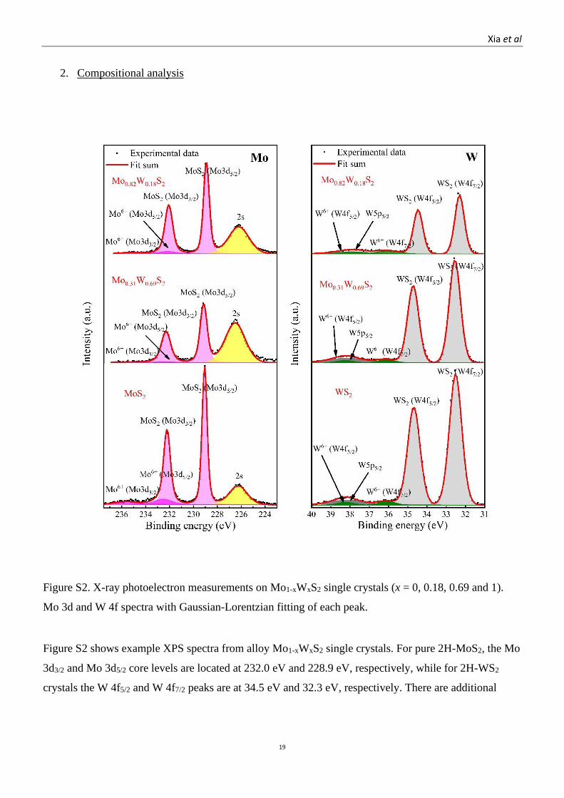
2. Compositional analysis
Figure S2. X-ray photoelectron measurements on Mo1-xWxS2 single crystals (x = 0, 0.18, 0.69 and 1).
Mo 3d and W 4f spectra with Gaussian-Lorentzian fitting of each peak.
Figure S2 shows example XPS spectra from alloy Mo1-xWxS2 single crystals. For pure 2H-MoS2, the Mo
3d3/2 and Mo 3d5/2 core levels are located at 232.0 eV and 228.9 eV, respectively, while for 2H-WS2
crystals the W 4f5/2 and W 4f7/2 peaks are at 34.5 eV and 32.3 eV, respectively. There are additional
Xia et al
20
doublet features at higher binding energies in the crystals that are associated to their oxidation states
(Mo-O and W-O), respectively. Compared to the pure materials, in the pristine 2H-Mo0.31W0.69S2, the
Mo 3d5/2,3/2 peaks and oxidised states shift to lower binding energies, while shifts of the W 4f7/2,5/2 peaks
of these states are very small. For the Mo rich end, both the Mo 3d5/2,3/2 and W 4f7/2,5/2 peaks shift to
lower binding energy, compared to the W rich and pure W materials. These observations are consistent
with previous reports.1,2 The stoichiometric ratio of W to (Mo + W) was calculated by integrating the
intensities of the Mo and W fitting peaks, applying standard sensitivity-factor corrections. As XPS is
surface sensitive, the crystals were also analysed by EDX to check for consistency in composition.
SEM-EDX was carried out in a Zeiss Gemini SEM 500 with an accelerating voltage of 5 kV and an
Oxford 150 EDS detector. The composition for the different alloys, obtained by SEM-EDX and XPS,
are summarised in Table S1.
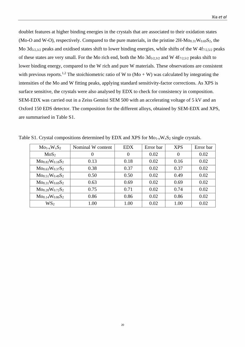
Table S1. Crystal compositions determined by EDX and XPS for Mo1-xWxS2 single crystals.
Mo1-xWxS2
crystals
Nominal W content
x
EDX Error bar XPS Error bar
MoS2 0 0 0.02 0 0.02
Mo0.82W0.18S2 0.13 0.18 0.02 0.16 0.02
Mo0.63W0.37S2 0.38 0.37 0.02 0.37 0.02
Mo0.51W0.49S2 0.50 0.50 0.02 0.49 0.02
Mo0.31W0.69S2 0.63 0.69 0.02 0.69 0.02
Mo0.28W0.72S2 0.75 0.71 0.02 0.74 0.02
Mo0.14W0.86S2 0.86 0.86 0.02 0.86 0.02
WS2 1.00 1.00 0.02 1.00 0.02

Xia et al
21
3. Monte Carlo simulations
Figure S3. (a) Atomic schematics of the different Mo(1-x)WxS2 atomic configurations used in the DFT calculations.
(b) Comparison between the binding energy calculated by DFT and that predicted using a pairwise interaction
calculated from an average value. For twenty Mo0.8W0.2S2 models generated with random configurations within
12×12×1 supercells, we also show (c) the DFT-calculated binding energy and (d) the difference ∆ (meV)
compared to the value expected based on the number of W-W bond (as would be measured in our Monte Carlo
model). These combine to verify that the energy model used in the Monte Carlo calculations represents a
reasonable approximation to the DFT results.

Xia et al
22
Figure S4. Monte Carlo simulation results showing the ratio of W-W pairs as a fraction of the total number of
TM-TM pairs for each nth-nearest neighbour shell, with pairwise interactions between nearest neighbours with J=
7.6 meV. Results are shown for a range of temperatures from T = 0 K to
T = 8000 K. At sufficiently low temperatures (T ≤ 50K), clear evidence is seen of long-ranged ordering, but this
ordering has almost vanished by the temperatures that will be encountered during the growth process (T ≈ 800 K).
Xia et al
23
4. Raman spectroscopy and photoluminescence of the Mo1-xWxS2 alloys
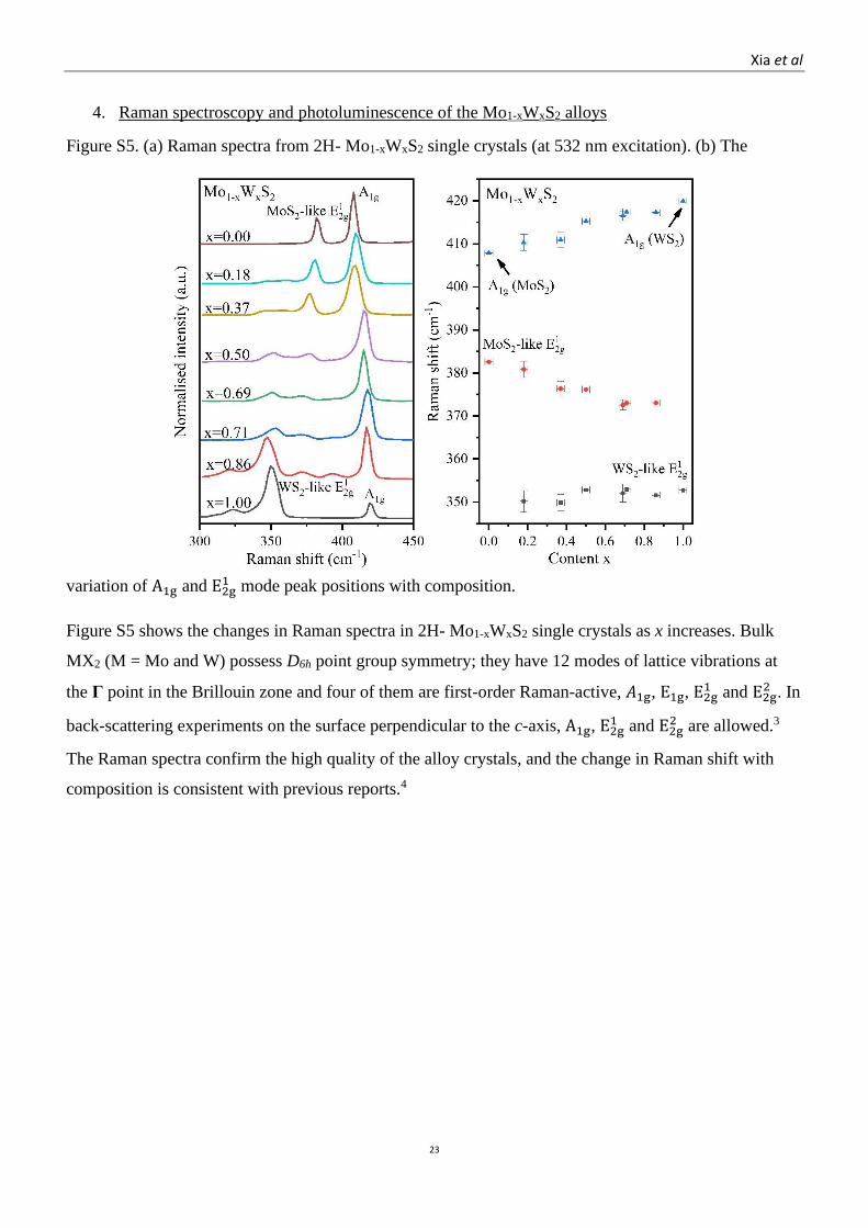
Figure S5. (a) Raman spectra from 2H- Mo1-xWxS2 single crystals (at 532 nm excitation). (b) The
variation of A1g and E2g1 mode peak positions with composition.
Figure S5 shows the changes in Raman spectra in 2H- Mo1-xWxS2 single crystals as x increases. Bulk
MX2 (M = Mo and W) possess D6h point group symmetry; they have 12 modes of lattice vibrations at
the Γ point in the Brillouin zone and four of them are first-order Raman-active, 𝐴1g, E1g, E2g1 and E2g
2 . In
back-scattering experiments on the surface perpendicular to the c-axis, A1g, E2g1 and E2g
2 are allowed.3
The Raman spectra confirm the high quality of the alloy crystals, and the change in Raman shift with
composition is consistent with previous reports.4
Xia et al
24
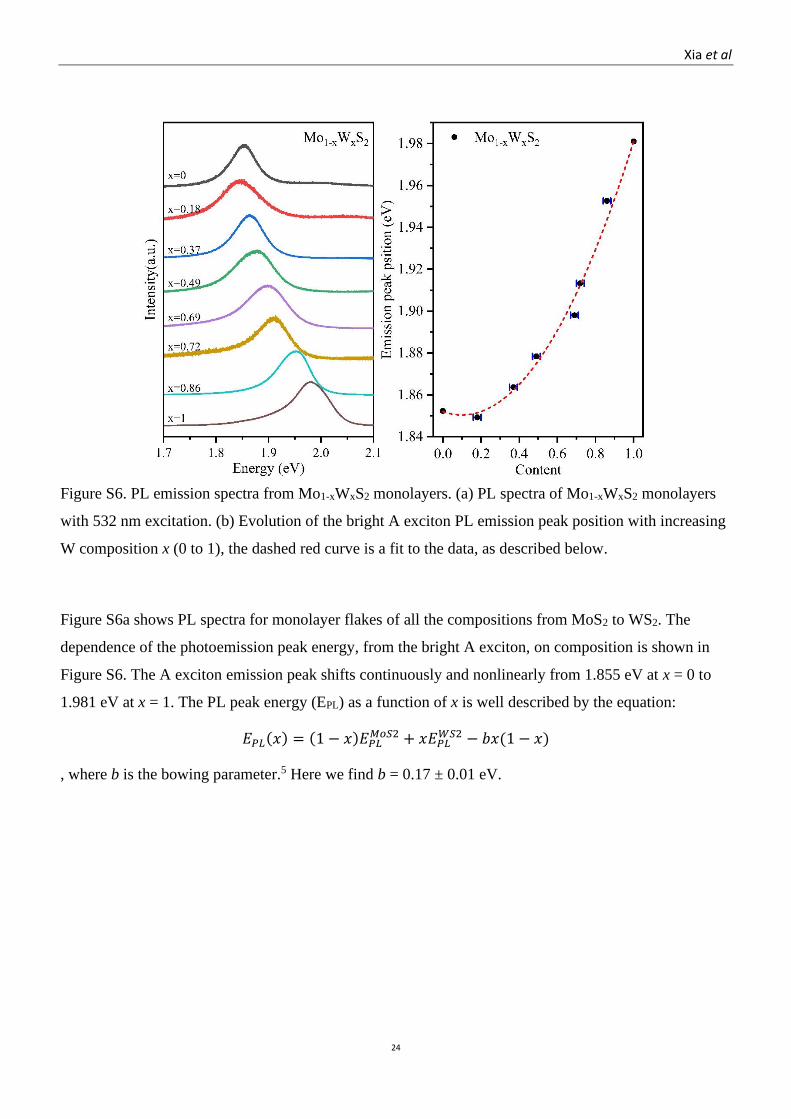
Figure S6. PL emission spectra from Mo1-xWxS2 monolayers. (a) PL spectra of Mo1-xWxS2 monolayers
with 532 nm excitation. (b) Evolution of the bright A exciton PL emission peak position with increasing
W composition x (0 to 1), the dashed red curve is a fit to the data, as described below.
Figure S6a shows PL spectra for monolayer flakes of all the compositions from MoS2 to WS2. The
dependence of the photoemission peak energy, from the bright A exciton, on composition is shown in
Figure S6. The A exciton emission peak shifts continuously and nonlinearly from 1.855 eV at x = 0 to
1.981 eV at x = 1. The PL peak energy (EPL) as a function of x is well described by the equation:
𝐸𝑃𝐿(𝑥) = (1 − 𝑥)𝐸𝑃𝐿𝑀𝑜𝑆2 + 𝑥𝐸𝑃𝐿
𝑊𝑆2 − 𝑏𝑥(1 − 𝑥)
, where b is the bowing parameter.5 Here we find b = 0.17 ± 0.01 eV.
Xia et al
25
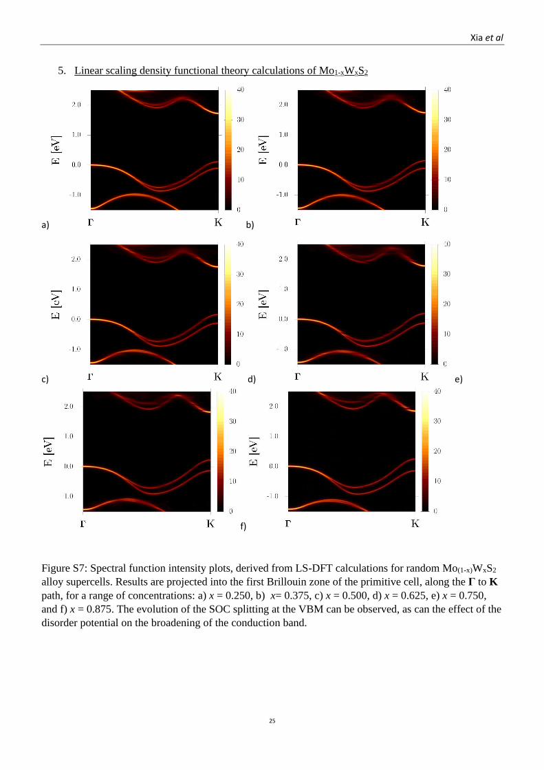
5. Linear scaling density functional theory calculations of Mo1-xWxS2
a) b)
c) d) e)
f)
Figure S7: Spectral function intensity plots, derived from LS-DFT calculations for random Mo(1-x)WxS2
alloy supercells. Results are projected into the first Brillouin zone of the primitive cell, along the Γ to K
path, for a range of concentrations: a) x = 0.250, b) x= 0.375, c) x = 0.500, d) x = 0.625, e) x = 0.750,
and f) x = 0.875. The evolution of the SOC splitting at the VBM can be observed, as can the effect of the
disorder potential on the broadening of the conduction band.

Xia et al
26
Figure S8: Estimate of the broadening of the conduction band induced by the disorder potential (red
line), as measured by the spread of CBM positions across different random realisations of the supercell,
compared to the SOC splitting on the conduction band (black). The magnitude of the disorder potential
exceeds the SOC for x<0.5.
Xia et al
27
6. References
(1) Wang, Z.; Liu, P.; Ito, Y.; Ning, S.; Tan, Y.; Fujita, T.; Hirata, A.; Chen, M. Chemical Vapor
Deposition of Monolayer Mo 1-x W x S 2 Crystals with Tunable Band Gaps. Sci. Rep. 2016, 6
(January), 2–10. https://doi.org/10.1038/srep21536.
(2) Gao, J.; Li, B.; Tan, J.; Chow, P.; Lu, T.-M.; Koratkar, N. Aging of Transition Metal
Dichalcogenide Monolayers. ACS Nano 2016, 10 (2), 2628–2635.
https://doi.org/10.1021/acsnano.5b07677.
(3) Zhang, X.; Qiao, X.; Shi, W.; Wu, J.; Jiang, D.; Tan, P. Phonon and Raman Scattering of Two-
Dimensional Transition Metal Dichalcogenides from Monolayer, Multilayer to Bulk Material.
Chem. Soc. Rev. 2015, 44 (9), 2757–2785. https://doi.org/10.1039/C4CS00282B.
(4) Dumcenco, D. O.; Chen, K. Y.; Wang, Y. P.; Huang, Y. S.; Tiong, K. K. Raman Study of 2H-
Mo1-XWxS2 Layered Mixed Crystals. J. Alloys Compd. 2010, 506 (2), 940–943.
https://doi.org/10.1016/j.jallcom.2010.07.120.
(5) Chen, Y.; Xi, J.; Dumcenco, D. O.; Liu, Z.; Suenaga, K.; Wang, D.; Shuai, Z.; Huang, Y. S.; Xie,
L. Tunable Band Gap Photoluminescence from Atomically Thin Transition-Metal Dichalcogenide
Alloys. ACS Nano 2013, 7 (5), 4610–4616. https://doi.org/10.1021/nn401420h.