On the Threat of Metastability in an Asynchronous Fault-Tolerant Clock Generation Scheme

Asynchronous Techniques for New
Generation Variation-Tolerant FPGA
Hock Soon Low
A Thesis Submitted for the Degree of Doctor of Philosophy
at Newcastle University
School of Electrical and Electronic Engineering
Faculty of Science, Agriculture & Engineering
October 2015
ii
Asynchronous Techniques for New Generation Variation-Tolerant FPGA ©
Hock Soon Low, Newcastle, October, 2015

iii
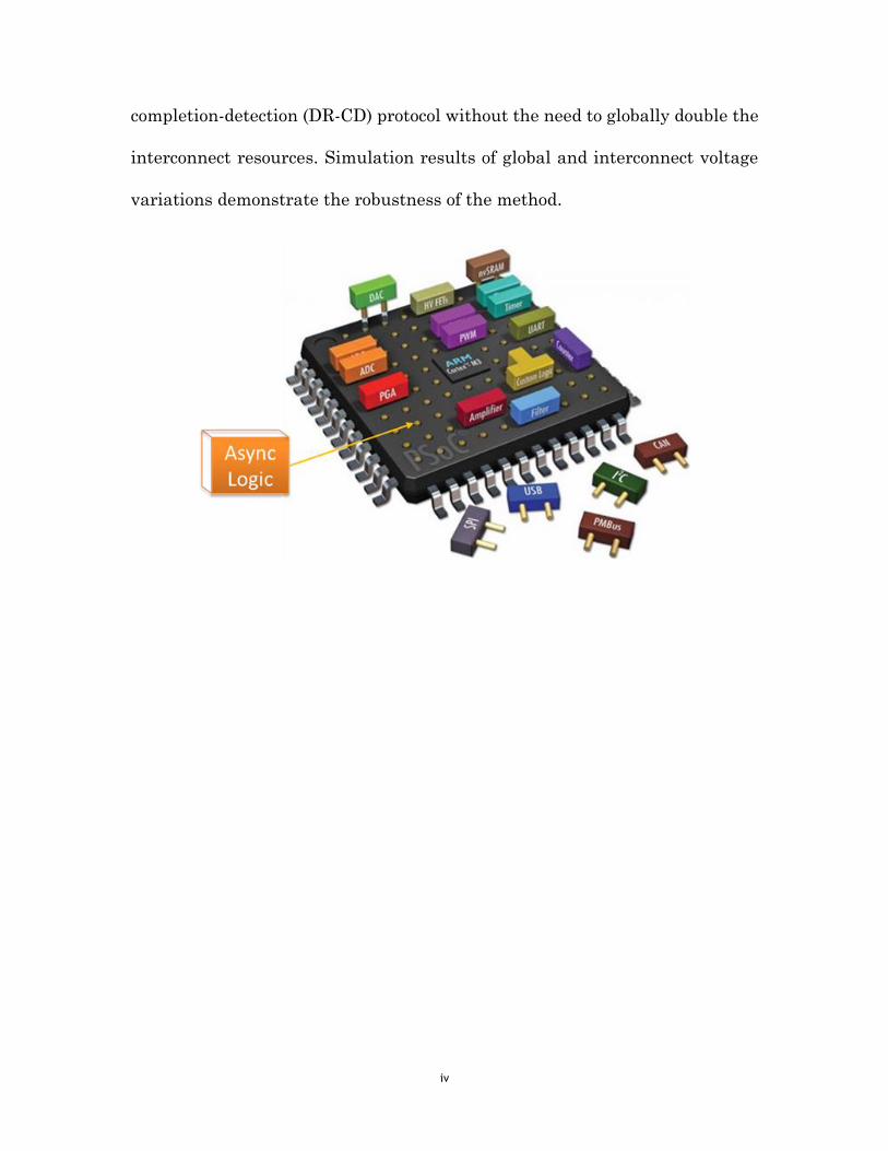
Abstract
This thesis presents a practical scenario for asynchronous logic
implementation that would benefit the modern Field-Programmable Gate
Arrays (FPGAs) technology in improving reliability. A method based on
Asynchronously-Assisted Logic (AAL) blocks is proposed here in order to
provide the right degree of variation tolerance, preserve as much of the
traditional FPGAs structure as possible, and make use of asynchrony only
when necessary or beneficial for functionality. The newly proposed AAL
introduces extra underlying hard-blocks that support asynchronous
interaction only when needed and at minimum overhead. This has the
potential to avoid the obstacles to the progress of asynchronous designs,
particularly in terms of area and power overheads. The proposed approach
provides a solution that is complementary to existing variation tolerance
techniques such as the late-binding technique, but improves the reliability of
the system as well as reducing the design’s margin headroom when
implemented on programmable logic devices (PLDs) or FPGAs. The proposed
method suggests the deployment of configurable AAL blocks to reinforce only
the variation-critical paths (VCPs) with the help of variation maps, rather than
re-mapping and re-routing. The layout level results for this method's worst
case increase in the CLB’s overall size only of 6.3%. The proposed strategy
retains the structure of the global interconnect resources that occupy the lion’s
share of the modern FPGA’s soft fabric, and yet permits the dual-rail
iv
completion-detection (DR-CD) protocol without the need to globally double the
interconnect resources. Simulation results of global and interconnect voltage
variations demonstrate the robustness of the method.

v
Acknowledgements
First of all, I would like express my profound thanks for my supervisors Prof
Alex Yakovlev for his support through the course of my studies. His wisdom
and vision were invaluable source of inspiration for me.
I would also like to express my gratitude to Dr Delong Shang and Dr Fei Xia
for their guidance and advice throughout my PhD.
I am also grateful to colleagues and friends in the Microelectronics System
Design research group at Newcastle University for their assistance and
inspiring working atmosphere. Dr Danil Sokolov, Dr XueFu Zhang, Dr Maxim
Rykunov, Dr James Docherty, Dr Graeme Coapes, Dr Nizar Dahir and Dr
Ra’ed Aldujaily and Dr Ghaith Tarawneh. They made my PhD journey more
enjoyable.
Finally, I wish to thanks my family for their love and unwavering support
through the duration of my studies.

vi
CONTENTS
CONTENTS ........................................................................................................ vi
FIGURES ............................................................................................................ xi
TABLES ............................................................................................................ xvi
1 Introduction .................................................................................................. 1
1.1 Motivation and Objective ........................................................................... 1
1.2 Overview of Chapters ................................................................................. 5
1.3 Contributions ............................................................................................. 6
1.4 Publications ................................................................................................ 7
Chapter 2. Background ....................................................................................... 9
2.1 Introduction ................................................................................................ 9
2.2 Introduction to FPGA Technology ........................................................... 10
2.2.1 Moore’s Law and Configuration Cells .............................................. 13
2.2.2 Programmable Memory ..................................................................... 14
2.2.3 Modern FPGA Fabric ........................................................................ 16
2.2.4 Software and Hardware Programmable Devices: ............................ 18
2.2.5 Difference between the FPGA and ASIC ......................................... 19
2.2.6 Summary of Evolution ...................................................................... 22
2.2.7 Fundamental Structure of the FPGA ............................................... 23
2.2.8 Logic Block ......................................................................................... 24
2.2.9 Routing Structure .............................................................................. 26
2.3 Introduction to Variation ......................................................................... 27
2.4 Classification of Variability ..................................................................... 28

vii
2.5 Process Variation Sources ........................................................................ 30
2.5.1 Tool-Related Variation ...................................................................... 31
2.5.2 Intrinsic Variation ............................................................................. 32
2.6 Environmental Variation ......................................................................... 33
2.6.1 Temperature Variation ..................................................................... 33
2.7 Temporal Variation – Ageing Related ..................................................... 38
2.8 Sensing and Characterisation ................................................................. 39
2.8.1 Off-chip Sensing ................................................................................ 40
2.8.2 On-chip Sensing ................................................................................ 41
2.8.3 Soft Sensing in FPGA ........................................................................ 43
2.9 Conventional Variation Tolerance in FPGAs .......................................... 44
2.9.1 STA and SSTA ................................................................................... 44
2.9.2 Optimisation of Structural Parameters ........................................... 46
2.9.3 Transistor Sizing ............................................................................... 46
2.9.4 Asynchronous Techniques ................................................................. 47
2.10 Variation Aware and Late Binding Techniques ................................... 48
2.10.1 Yield Improvement Through Multiple-Configuration ................... 49
2.10.2 Variation Aware Modelling ............................................................. 50
2.10.3 Relocation, Remapping and Rerouting ........................................... 52
2.11 Summary ................................................................................................ 53
Chapter 3. Existing Asynchronous Techniques in FPGA ................................ 58
3.1 Introduction .............................................................................................. 58
3.2 Principles of Asynchronous Design .......................................................... 59
3.3 Bundle Data Design ................................................................................. 60

viii
3.3.1 Single-Rail Bundle-Data (SR-BD) .................................................... 61
3.3.2 4-Phase and 2-Phase Bundle-Data Handshaking ............................ 62
3.4 Delay-Insensitive Encoding ..................................................................... 65
3.4.1 4-Phase Dual-Rail Handshaking ...................................................... 66
3.4.2 Completion Detection (CD) Circuit ................................................... 68
3.4.3 2-Phase Dual-Rail Protocol ............................................................... 69
3.5 Asynchronous Circuit Classification: ...................................................... 70
3.5.1 Speed–Independent (SI) .................................................................... 71
3.5.2 Delay-Insensitive (DI) ....................................................................... 72
3.5.3 Quasi-Delay-Insensitive (QDI) ......................................................... 72
3.6 Reconfigurable Asynchronous Architectures ........................................... 73
3.6.1 Type 1: Bundle Data and Timing Assumption Architectures ......... 74
3.6.2 Type 2: High Performance Architecture ........................................... 77
3.6.3 Type 3: Communication Efficiency (2-Phase Dual-Rail or LEDR) .. 79
3.6.4 Type 4: Hierarchical and Coarse Grain Reconfigurable Architecture
..................................................................................................................... 82
3.6.5 Other Asynchronous Style FPGAs ................................................... 86
3.7 Summary .................................................................................................. 89
Chapter 4. Distributed Control Asynchronous FPGA Architecture ................ 93
4.1 Introduction .............................................................................................. 93
4.2 Asynchronous Wrapper ............................................................................ 94
4.3 Top Level Overview of the Architecture ................................................... 96
4.4 Asynchronous Wrapper Structure ........................................................... 98
4.4.1 Programmable Completion Detection (PCD) ................................. 101

ix
4.4.2 Switch Box (SW) Circuit ................................................................. 102
4.4.3 Programmable Delay (PD) Unit ..................................................... 103
4.4.4 Single-Rail to Dual-Rail Conversion Circuit (CONV) .................... 104
4.5 Area, Power and Speed Performance ..................................................... 105
4.5.1 Area Overhead Calculation ............................................................. 105
4.5.2 Power Comparison .......................................................................... 106
4.5.3 Throughput Performance ................................................................ 111
4.6 Variability Evaluation ........................................................................... 112
4.6.1 PLE Characterisation with Variable Vdd ...................................... 112
4.6.2 Corner Analysis for PVT Variation ................................................ 115
4.7 Logic Cluster Design .............................................................................. 117
4.7.1 Distributed Control with David Cell .............................................. 119
4.7.2 David Cell Control Transition Flow ............................................... 122
4.7.3 Implementation Case Study ........................................................... 124
4.7.4 Design Flow ..................................................................................... 127
4.8 Summary ................................................................................................ 131
Chapter 5. Asynchronously Assisted Logic (AAL) Scheme............................ 134
5.1 Introduction ............................................................................................ 134
5.2 Architecture Overview ............................................................................ 135
5.3 AAL Architecture Implementation ......................................................... 137
5.4 Area Overhead Calculation ................................................................... 138
5.5 Multi-Style Handshaking Support ........................................................ 140
5.6 Proposed Variation Aware Design Flow ................................................ 144
5.7 Throughput and Operation Energy Study ............................................ 145

x
5.7.1 Short Critical Path .......................................................................... 146
5.7.2 Long Critical Path ........................................................................... 148
5.8 Variability Study ................................................................................... 150
5.8.1 Global Variability Simulation ......................................................... 151
5.8.2 Interconnects Variability Simulation ............................................. 153
5.9 System Design on AAL structure ........................................................... 155
5.9.1 Handshaking Support for Data Flow Structures ........................... 155
5.9.2 Booth Multiplier Case Study .......................................................... 157
5.10 Summary .............................................................................................. 160
Chapter 6. Conclusion ..................................................................................... 162
6.1 Summary of Thesis ............................................................................. 162
6.2 Future Work ........................................................................................ 165
6.1.1 Variation Aware Design Flow with Consolidated Variation Map . 165
6.1.2 GALS Scheme Support .................................................................... 165
6.1.3 Silicon Implementation ................................................................... 166
Appendix A: Abbreviations ............................................................................. 168
Appendix B: AAL Implementation ................................................................. 171
Appendix C: Input Vector for Candence ......................................................... 172
Appendix D: Sawtooth Vdd Generation ......................................................... 173
Appendix E: Variation Map Generation ......................................................... 174
Bibliography .................................................................................................... 175
Tables
xi
FIGURES
Figure 1: Design margin barriers to efficiency. ................................................. 1
Figure 2: Asynchronous handshaking overhead and elastic margin’s
headroom. ............................................................................................................ 2
Figure 3: Theoretical graph of relative cost of elasticity and handshaking
protocols. .............................................................................................................. 4
Figure 4: (a) PLA with programmable OR plane; (b) PAL with fixed OR plane
[9]. ...................................................................................................................... 11
Figure 5: (a) Look-Up Table (LUT) Structure, (b) 6-Transistors SRAM Cell. 13
Figure 6: Modern FPGA fabric with Hard-block .............................................. 18
Figure 7: Basic FPGA and ASIC design flow[17]. ............................................ 20
Figure 8: Key technology comparison vectors. ................................................. 22
Figure 9: Basic logic implementation on the primary logic cell: (a) logic
diagram of a 1-bit adder; (b) truth-table for SUM; (c) logic mapping on a
lookup-table (LUT). ........................................................................................... 25
Figure 10: Hierarchy view of FPGA structure: (a) Island style structure, (b)
Two slices in a CLB, (c) Basic LC structure. .................................................... 26
Figure 11: Routing resources structure. ........................................................... 27
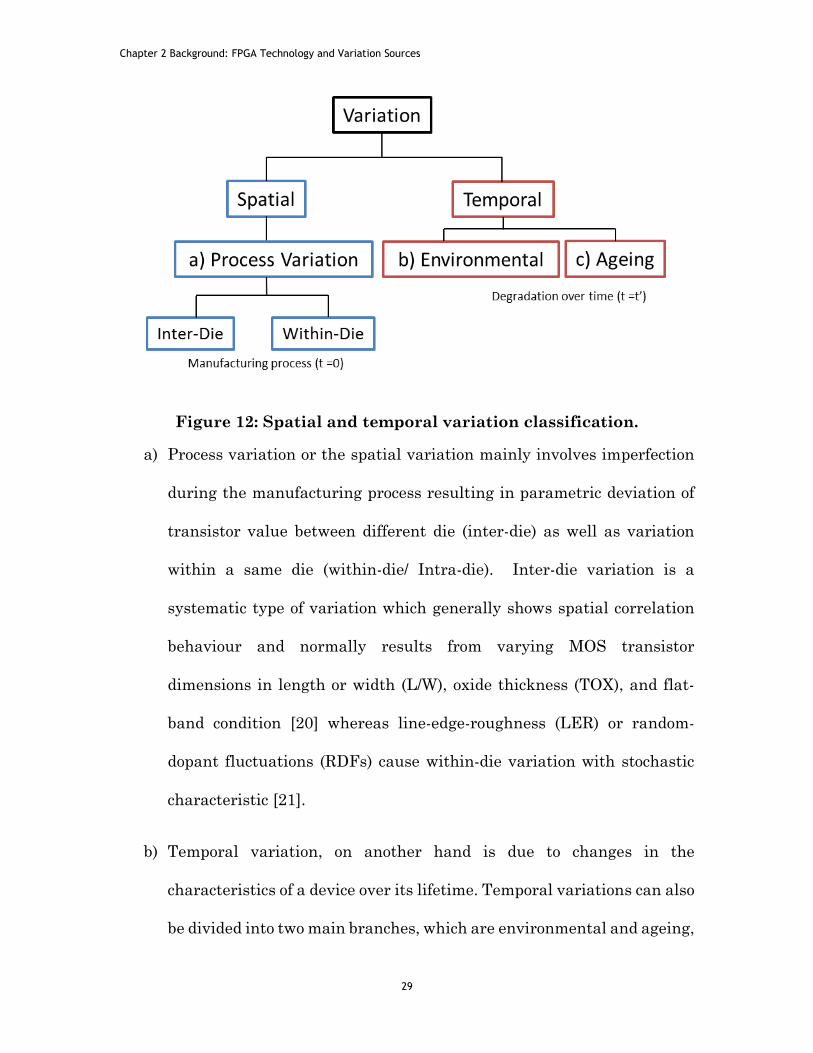
Figure 12: Spatial and temporal variation classification. ............................... 29
Figure 13: Subdivisions of process variation. ................................................... 31

Tables
xii
Figure 14: Line edge roughness at 90nm and 22nm technology [23]. ............. 33
Figure 15: Classification of sources of environmental variation. .................... 33
Figure 16: Inverse path delay characteristics at lower voltage level with
increase in temperature [29]. ............................................................................ 35
Figure 17: Ageing related temporal variation. ................................................. 38
Figure 18: Corner analysis with STA tools ...................................................... 45
Figure 19: Multiple reconfiguration strategy flow. .......................................... 49
Figure 20: Variation aware chipwise placement design flow [72]. .................. 51
Figure 21: (a) Region relocation, (b) Path reconfiguration. ............................. 52
Figure 22: Synchronous clocking system.......................................................... 60
Figure 23: Abstract view of Asynchronous Circuit. ......................................... 60
Figure 24: (a) Abstract view of delay matching bundle-data approach; (b)
example of programmable delays bank. (c) AND gate and muxes fine tune
programmable delay [82]. ................................................................................. 61
Figure 25: Send and receive handshaking. ...................................................... 62
Figure 26: (a) 4-phase bundled-data protocol; (b) 2-phase bundled-data
protocol [83]. ...................................................................................................... 63
Figure 27: (a) Request sign embedded in dual-rail coding; (b) the codewords;
(c) signal transition waveform; (d) code with Hamming distance = 1. ............ 66
Figure 28: (a) Example of dual-rail completion detection circuit; (b) truth
table for the C-element. ..................................................................................... 69

Tables
xiii
Figure 29: Case study of delay model circuit classification. ............................ 71
Figure 30: MONTAGE functional unit (configured as C-Muller gate). .......... 75
Figure 31: PGA-STC functional block with programmable delay element. .... 76
Figure 32: PAPA architecture logic block [98]. ................................................ 77
Figure 33: 4P-DR and LEDR communication. ................................................. 80
Figure 34: LUT4-based phased logic gate [115]. .............................................. 81
Figure 35: More complex LEDR protocol converter [117]................................ 82
Figure 36: GALS in FPGA: (a) Homogeneous; (b) Heterogeneous. ................. 83
Figure 37: (a) Basic reconfigurable NCL LE; (b) 27 fundamental NCL gates
[127]. .................................................................................................................. 87
Figure 38: Island style architecture. ................................................................ 96
Figure 39: Wrapper based programmable logic element (PLE). ..................... 99
Figure 40: Programmable completion detection. ........................................... 101
Figure 41: SW box circuit. ............................................................................... 103
Figure 42: Programmable delay circuit. ......................................................... 103
Figure 43: Dual-rail conversion or DEMUX circuit ....................................... 104
Figure 44: (a) Synchronous LUT; and (b) PCD asynchronous LUT. ............. 107
Figure 45: Operation power: (a) synchronous LUT with timing clock; (b)
asynchronous LUT with PCD. ........................................................................ 109

Tables
xiv
Figure 46: Delay and operational energy at below nominal Vdd level: (a)
results table; (b) delay and energy plot over Vdd. ......................................... 113
Figure 47: PLE working under variable Vdd. ................................................ 115
Figure 48: PD and LUT delay successfully bundling: (a) Slow corner
(temperature=400K). (b) Fast corner (temperature=273K)........................... 117
Figure 49: Cross over at (sf): corner (a) Temperature=300K. (b)
Temperature=273K. ........................................................................................ 117
Figure 50: Logic cluster with DC. ................................................................... 119
Figure 51: (a) Basic David cell Structure; (b) DC for distributed control; (c) set
and reset logic boxes for DC implementations. .............................................. 121
Figure 52: Data flow transition example with DCs. ...................................... 122
Figure 53: Four bit full Adder example. ......................................................... 125
Figure 54: System design flow. ....................................................................... 129
Figure 55: Petri net models of control elements. ........................................... 130
Figure 56: Architecture overview: (a) Island style architecture, (b) AAL
within a CLB. .................................................................................................. 136
Figure 57: AAL plugin to Xilinx’s CLB with SLICEL & SCLICEX. ............. 137
Figure 58 Area calculation of CLB with AAL. ............................................... 138
Figure 59: Dual-Rail Completion-Detection (DR-CD) resources. .................. 141
Figure 60: Four Stages implementation of DR-CD circuit. ........................... 142

Tables
xv
Figure 61: Single-Rail Bundle-Data (SR-BD) resources. ............................... 143
Figure 62 Four Stages implementation of SR-BD circuit. ............................. 143
Figure 63: Clock triggers switching. ............................................................... 144
Figure 64: Design flow based on variation map. ............................................ 145
Figure 65: Test setup for 4RCA. ..................................................................... 147
Figure 66: Throughput and energy comparison (Voltage sweep, 0.4 - 1.0v), (a)
Throughput (Counts), (b) Operation Energy (pJ). ......................................... 148
Figure 67: Test setup for 16RCA and 4x4RCA. ............................................. 149
Figure 68: Global Vdd variation simulation setup. ....................................... 151
Figure 69: Correct operation under various viable voltage supplies. ........... 152
Figure 70: Mixed constant Vcc on CLB and variable Vdd on interconnect
simulation. ....................................................................................................... 153
Figure 71: Interconnect variation simulation results .................................... 155
Figure 72: Block diagram of Booth multiplier. .............................................. 158
Figure 73 : Petri-net representation of booth multiplier control flow. .......... 158
Figure 74: Simplified SR-BD handshaking diagram for Booth multiplier. .. 158
Figure 75: Simulation waveform of Booth multiplier implementations. ...... 159

Tables
xvi
TABLES
Table 1: Key configurable cells technology comparison[9]. ............................. 16
Table 2: Summary of asynchronous FPGAs ..................................................... 73
Table 3: Choice of architecture structure. ........................................................ 97
Table 4: Dual-rail code-words. ........................................................................ 101
Table 5: PLE size in terms of number of transistors. .................................... 105
Table 6: Power and energy comparison. ......................................................... 110
Table 7: Throughput comparisons of various architectures. ......................... 111
Table 8: Overhead of various asynchronous schemes. ................................... 139
Table 9: Comparison result for short path (4RCA). ....................................... 147
Table 10: Throughput and energy performance. ............................................ 149
Table 11: Data flow control elements. ............................................................ 156

Chapter 1: Introduction
1
1 Introduction
1.1 Motivation and Objective
The effects of variability have become increasingly significant as a result of the
scaling of technology. Static and dynamic variations affect the reliability of
integrated circuits. Conservative approaches to increases the timing-
margin/guard-band across the whole chip is imprudent and degrades
performance. Figure 1 shows that excessive design margins to guarantee
correct circuit operation over fix periods for both spatial and temporal
variations are wasteful and reduced the circuit’s efficiency in a synchronous
system [1, 2]. (Note: the scale of the margins in Figure 1 and Figure 2 are for
illustration only and may not scale accordingly).
Figure 1: Design margin barriers to efficiency.
FPGAs may be more affected compared to Application-specific integrated
circuit (ASIC) because the circuit mapping and critical path vary depending on

Chapter 1: Introduction
2
user design in post-fabrication [3]. Therefore various traditional variation
tolerance techniques proposed for ASICs may not be directly applicable. Yet,
due to its configurability, the FPGA presents a unique opportunity to address
variability and reliability challenges [4, 5].
Asynchronous designs are highly tolerant to voltage and delay changes, and
have been shown to be very robust in the present of variations [6, 7]. This also
gives the potential for efficiency improvements in the margin headroom as
shown in Figure 2. Therefore, applying asynchronous logic to FPGAs is an
attractive idea.
Figure 2: Asynchronous handshaking overhead and elastic margin’s
headroom.
However, there are three major challenges in applying asynchrony in
balancing between the handshaking overhead and level of tolerances, as
illustrated in Figure 2 . These challenges are as follows:
i. Asynchronous circuits are more difficult to design and test compare to
synchronous ones because of the wide variety of possible signalling

Chapter 1: Introduction
3
protocols and a broad spectrum of the degree of delay insensitivity from
bounded-delay to fully delay insensitive (DI). Partly because of this,
asynchronous designs suffer from a lack of automatic design tools,
especially those combining all possible techniques in a single suite.
These issues have impeded the progress of asynchronous techniques in
the FPGA, because the latter is intrinsically less customizable.
ii. Asynchronous circuit is normally higher in area and power overheads
due to the extra circuitry needed for handshaking. This depends on the
delay assumption made or the protocols used. For example, converting
all of the communication to dual-rail will double the interconnect
resources. This is not acceptable, since interconnects occupy the lion’s
share of the fabric.
iii. Depending on the timing assumptions made or handshaking protocols
used, asynchronous logic can provide a range of improvements in power
and speed/throughput efficiency in addition to its robustness toward
variability. For instance, a single-rail delay-matching (SR-DM) protocol
is more efficient in terms of power and area but more susceptible to
variation compared to the 4-phase dual-rail (4P-DR) scheme which is
more robust to variation but may require higher power and area as
shown in theoretical graph in Figure 3 – relative cost of elasticity and
handshaking protocols. Similar project of cost of elasticity using
different asynchronous tools also presented in [8].

Chapter 1: Introduction
4
Figure 3: Theoretical graph of relative cost of elasticity and
handshaking protocols.
Therefore the objective of this thesis is centred on strategies which can
maximise the variation tolerance benefit and keep the overhead at a balance.
The challenges mentioned above are addressed using the following approaches:
i. A wrapper-based asynchronous logic approach to communication and
the preservation of the LUT-based computation block of modern FPGA
architecture. This allows the re-use of the major part of the design tool
flow, particularly the logic packing and mapping. It seeks to achieve
delay insensitive (DI) in the large for long inter-cluster wires and speed
independence (SI) in the small within clusters.
ii. Characterising the performance of the most popularly used
handshaking protocols that are tailored for reconfigurable logics. The
power, throughput, area and robustness are determined of protocols

Chapter 1: Introduction
5
such as 4-phase dual-rail (4P-DR), 2-phase dual-rail (2P-DR), and
bundled-data (BD).
iii. A strategy to balance the use of asynchrony to tolerate the effects of
variations and the minimization of the area and power overheads.
1.2 Overview of Chapters
Chapter 2 gives an introduction to the development of programmable logic
devices (PLDs) and their evolution into today’s modern FPGA architectures.
The continued scaling of CMOS technology enables the development of many
advanced technologies. However the associated challenges include increasing
variability problems in the manufacturing process as well as the effects of
degradation effects over time. The second part of the chapter classifies the
sources of variability and reviews its impact on FPGA structure as well
existing techniques which attempt to reduce the impact.
Chapter 3 presents a literature review of the use of asynchronous approaches.
The fundamental theory and terminology of asynchronous design are also
briefly introduced here to serve as a basis for further understanding of the
following chapters.
Chapter 4 describes the distributed control architecture which retains the
computational block of the traditional FPGA un-touched (single-rail) and
proposes the asynchronous wrapper and David’s cell control around it. The
Chapter 1: Introduction
6
result achieves a balance between the desire to use asynchrony for tolerate the
effects of variations and retention of the major part of the current design flow.
Chapter 5 presents new concepts for addressing the overhead challenges with
an on-demand strategy. This approach suggests the deployment of
asynchronous logic only on variation-critical paths (VCPs) by leveraging the
mature techniques in obtaining variation maps. The proposed integration of
asynchronously assisted logic (AAL) with state of the art FPGA architecture
involves a minimal increase in overhead. Furthermore, the AAL supports the
use of multi-style asynchronous logic implementation to allow the exploration
of asynchrony at different levels of variation.
Chapter 6 summarises the techniques presented and describes the outlook for
future developments.
1.3 Contributions
Classification of sources of the variability and its impact on FPGA
architecture (chapter 2)
Survey of asynchronous reconfiguration architectures based on the
protocols and delay assumption used (Chapter 3)
A detailed circuit realization at components level for the asynchronous
wrapper using the distributed control approach for asynchronous
components (Chapter 4)

Chapter 1: Introduction
7
The proposal of a novel AAL architecture that applied Asynchrony only
on the VCPs for the balancing of resource overhead and variation
tolerance (Chapter 5)
Summaries the work and proposed techniques for advancement.
(Chapter 6)
1.4 Publications
The following papers have been published during the course of this work:
H. S. Low, D. Shang, F. Xia, and A. Yakovlev, "Variation tolerant asynchronous
FPGA", poster presented at the 19th ACM/SIGDA International Symposium
on Field-Programmable Gate Arrays (FPGA 2011) conference, Monterey,
California, pp 282, 2011.
H. S. Low, D. Shang, F. Xia, and A. Yakovlev, "Variation tolerant AFPGA
architecture", presented at the 17th IEEE International Symposium
Asynchronous Circuits and Systems (ASYNC 2011), Ithaca, NY, pp 77–86, 2011.
X. Zhang, D. Shang, F. Xia, H. S. Low, and A. Yakovlev, "A hybrid power
delivery method for asynchronous loads in energy harvesting systems", in
IEEE 10th International New Circuits and Systems (NEWCAS 2012)
conference, Montreal, Canada, pp 413-416, 2012.

Chapter 1: Introduction
8
H. S. Low, D. Shang, F. Xia, and A. Yakovlev, "Asynchronously Assisted FPGA
for Variability", poster presented at the Field Programmable Logic and
Applications (FPL 2014) conference, Munich, Germany, 2014.

Chapter 2 Background: FPGA Technology and Variation Sources
9
Chapter 2. Background
2.1 Introduction
Field-programmable Gate Arrays (FPGAs) have become a popular technology
for implementing digital electronic systems today due to their re-
configurability nature and short design cycle. Continued technology scaling
enables more and more features to be implemented in a same size form-factor.
However, similar to other VLSI design, many new challenges emerged due to
the continued scaling of CMOS process technology. Variability and reliability
have become growing issues in the nanometre scale region.
In order to understand the impact of variation on FPGA architecture, this
chapter first provides an overview of FPGA technology and its development in
recent years. Variation can be from many sources due to imperfection of
manufacturing process, environmental changes or ageing effect resulting in
correlated and random behaviour. This chapter also serves to clarify the terms
by classification of the variability sources and technique commonly used to
characterise them. On-chip, off-chip and soft-sensing classification techniques
will be reviewed.
With the understanding of the variability through the characterisation
techniques available from industry as well as academic research,
improvements of performance and yield can be achieved through variation
aware techniques that are unique for reconfigurable architectures such as

Chapter 2 Background: FPGA Technology and Variation Sources
10
FPGA. The remainder of the chapter is structured into the following
subsections:
i. Introduction to FPGA Technology
ii. Classification of Variability Sources
iii. Sensing and Characterisation Techniques
iv. Variation-tolerant and Yield Improvement Techniques
2.2 Introduction to FPGA Technology
The FPGA is a hardware programmable device whose function can be defined
after fabrication. The concept of the reconfigurable logic device was introduced
in the electronic system design market in 1980s. The reason for the initial
development of reconfigurable devices was mainly to ease the challenges faced
by the traditional board-level design with standard components that increased
in number with circuit complexity and size. The amount of components and
layers of printed circuit boards (PCBs) grew drastically and thus the chance
interconnection errors occurring increased together with the pressure on
create a small form factor to fit the components into the enclosure.
Fuelled by the fast-moving market and evolving standards and rising of mask
development costs in the manufacturing applications-specific integrated
circuits (ASIC), the concept of the programmable logic device (PLD) that would

Chapter 2 Background: FPGA Technology and Variation Sources
11
allow its functionality to be restructured was born and has served the basis for
more advance in PLDs.
The programmable logic array (PLA) was one of the earliest types of PLD.
Figure 4 (a) shows a typical structure of a PLA consisting of a matrix of
programmable AND-gates and OR-gates in a plane used to implement the
minimised standard forms of Boolean expressions, which are sum-of-products
functions.
Figure 4: (a) PLA with programmable OR plane; (b) PAL with fixed
OR plane [9].
Chapter 2 Background: FPGA Technology and Variation Sources
12
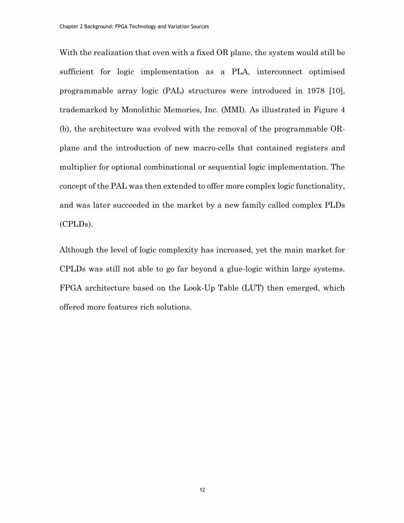
With the realization that even with a fixed OR plane, the system would still be
sufficient for logic implementation as a PLA, interconnect optimised
programmable array logic (PAL) structures were introduced in 1978 [10],
trademarked by Monolithic Memories, Inc. (MMI). As illustrated in Figure 4
(b), the architecture was evolved with the removal of the programmable OR-
plane and the introduction of new macro-cells that contained registers and
multiplier for optional combinational or sequential logic implementation. The
concept of the PAL was then extended to offer more complex logic functionality,
and was later succeeded in the market by a new family called complex PLDs
(CPLDs).
Although the level of logic complexity has increased, yet the main market for
CPLDs was still not able to go far beyond a glue-logic within large systems.
FPGA architecture based on the Look-Up Table (LUT) then emerged, which
offered more features rich solutions.

Chapter 2 Background: FPGA Technology and Variation Sources
13
2.2.1 Moore’s Law and Configuration Cells
Figure 5: (a) Look-Up Table (LUT) Structure, (b) 6-Transistors SRAM
Cell.
Gordon Moore, co-founder of Intel, forecast in his 1965 paper, “Cramming more
components onto integrated circuits” [11] that the cost of transistors in a silicon
chip would continue to fall with every advance of technology every two years
or so, and later the prediction turned into a self-fulfilling prophecy. The
doubling of numbers of transistors every 18 months following Moore’s Law has
stimulated drastic growth in the electronics industry. The doubling of
transistor number at a rapid rate has also meant reductions in the cost per
transistor with every new generation of smaller transistors. This benefited the
advances in FPGA technology in the market in the mid-1980s. This is because
the LUT-based FPGA, as in Figure 5 (a), used static-random-access-memory
(SRAM) as the basis of the architecture and the typical SRAM circuit requires
six transistors, as shown in Figure 5 (b), which means the configuration
memory cell comes with a high overhead. However, with the growth indicated
by Moore’s Law, up to this point this has led the industry to exploit transistors

Chapter 2 Background: FPGA Technology and Variation Sources
14
which are almost free, especially in programmable hardware devices. This
validated the area and cost overhead issue on SRAM-based FPGA.
2.2.2 Programmable Memory
Programmable memory or the configuration cells are the underlying
technology for hardware configurability. Earlier PLD devices used
programmable read-only memory (PROM) where the programming could only
be done once and was irreversible; namely the on-time-programmable (OTP)
memory. Anti-fuse memory type, which is one, is more beneficial in terms of
lower area, resistance and capacitance compared to others. Because it is a non-
volatile memory, this means that the system can work instantly at power-up
in contrast to SRAM. In addition, the prime advantage of the anti-fuse PLD
and the FPGA are their susceptibility to faults in environment with heightened
radiation. In particular, the Actel/Microsemi [12] PLDs dominated the military
and aerospace markets for over fifteen years [13]. However, the main
disadvantage of anti-fuse FPGAs is that it requires specialised manufacturing
and programming mechanism. This make it not in-system programmable as
opposed to SRAM, which can fit well within the standard CMOS
manufacturing process, the anti-fuse technology cannot scale and advance at
the same rate as CMOS devices, making it far behind the process geometry in
many generation in comparison.

Chapter 2 Background: FPGA Technology and Variation Sources
15
An alternative Non-volatile memory that supports multiple re-write cycles and
is convenient for in-system programming is the EEPROM (electrically erasable
programmable read-only-memory) or flash memory. Technically this is a type
of EEPROM but offers higher speed when writing large amounts of data
compared to non-flash EEPROM memory. In addition, flash memory also offers
fast read access times similar to DRAM (dynamic RAM) but slower than SRAM.
The key advantages of flash based FPGA over SRAM are its low power
requirement, non-volatility and it is also more secure and reliable for IP
(intellectual property) protection purposes from a security standpoint as no
extra external configuration memory required upon start since SRAM is
volatile and cannot hold the data at power lost. However, the disadvantages of
flash memory are its limited write cycle and the fact that specific
manufacturing processes are used which differ from standard CMOS
technology.
SRAM is the most popular type of memory used in today’s FPGAs for two
primary reasons. First, it offers the unlimited in-system programming and
second the standard CMOS process technology is used and therefore, it benefits
from the advances of the latest scaling of CMOS technology. However,
continuous technology scaling may also have adverse impacts, which are
discuss later in this chapter.
Unlike flash-based non-volatile devices, the volatile SRAM-based FPGA
cannot hold its configuration without power source. Therefore, a dedicated

Chapter 2 Background: FPGA Technology and Variation Sources
16
programming circuity and sequence is needed to load the configuration bits at
every system power-up. This also means that SRAM-based FPGA has a lead-
time at power-up before live operation and requires extra board-level non-
volatile components, which increase the overall cost. Since the configuration
data are stored externally, this also opens up the potential for IP protection
issues, although alternative encryption solutions may eliminate this. A
summary and comparison of these three main types of memory are show in
Table 1.
Table 1: Key configurable cells technology comparison[9].
Memory Type Anti-fuse Flash SRAM
Features
Non-Volatile Yes Yes No
Reconfigurable Cycle one-time Limited Unlimited
Area (element size) Low Moderate High
In-System programing No Yes Yes
Manufacturing Process Anti-fuse custom Flash process Standard CMOS
Speed Fast read, slow write Fast read, slow rewrite Fast
2.2.3 Modern FPGA Fabric
The tradition basic FPGA architecture consisting only of reconfigurable logic,
an interconnect block and the input/output (I/O) pad is call soft fabric. Today’s
state-of-the-art PFGAs are packed with over a million LUTs. Also more and

Chapter 2 Background: FPGA Technology and Variation Sources
17
more hard blocks have been included in the package to improve computation
performance, including the digital-signal-processing (DSP) block, distributed
memory, high-speed communication links, and an advanced clock management
system together with mixed signal analogue functionality. This has made the
architecture increasingly heterogeneous as illustrated in Figure 6. In hybrid
structures, combinations of hard and soft microprocessor cores are also
included. With the advances in FPGA technology, the use of mature
intellectual property (IP) and computer-added-design tools (CAD) have also
facilitated the emergence of user customisable system-on-chip (SoC) FPGAs
that provide significant benefits for embedded system implementation.

Chapter 2 Background: FPGA Technology and Variation Sources
18
Figure 6: Modern FPGA fabric with Hard-block
2.2.4 Software and Hardware Programmable Devices:
Compared to general-purpose microcontrollers and microprocessors (µPs),
FPGA-based circuit implementation is typically much faster. This is because
in the FPGA, It is not necessary for the controller to move the data around
between the data memory and working register in order to perform logic
operations or in the context terms, the sequential fetch-decode-execute loop of
soft-computation. The classic examples of software-programmable
architectures are Von Neumann and Harvard processors. Instead, the
underlying computation in FPGA is hardware-based. All of the possible
combinations of output from a set of inputs is pre-calculated with Boolean
algebra expression in a truth table and Karnaugh map and stored in the LUTs.
The arrival of inputs will essentially become the address pointer to the specific

Chapter 2 Background: FPGA Technology and Variation Sources
19
memory location of the LUT; therefore, complex and multiple iteration
computations can be avoided and results can be obtained almost instantly.
Similar techniques have also been used in microcontrollers to achieve the fast
computation of complex calculations by using the “not-to-compute-all”
technique or, in other words prefetching or pre-calculating and storing all
possible results on LUTs[14]. This technique is very effective and commonly
used in embedded system design to decrease computation time. In the FPGA,
LUT techniques are exploited intensively across the whole architecture.
2.2.5 Difference between the FPGA and ASIC
The application-specific integrated circuit (ASIC) is a general term for fully
customised designs. The main benefit of a device that is fully custom-designed
is its smaller form factor from its manufacturing specifications and lower cost
for high volume production. Whereas the FPGA is a hardware programmable
device that its functionality can be configure by the end user after fabrication,
which explains the term “field-programmable”. The key advantages of the
FPGA over ASIC are the low non-recurring engineering cost, which support
rapid prototyping and fast-time-to-market. However, the disadvantage is that
the FPGA may not be suitable for most electronic system design specifications
because FPGAs are used for general purposes and therefore the logic density
of the chip is multiple folds below that of the ASIC design. This translates into
higher power consumption, higher cost and slower speed performance
compared to equivalent systems implemented with ASIC. However, due to the

Chapter 2 Background: FPGA Technology and Variation Sources
20
advancement of CMOS processes and the introduction of more “hardened”
blocks such as multipliers and accumulators, the performance gap between
FPGAs and ASICs is gradually becoming smaller [15, 16].
Figure 7: Basic FPGA and ASIC design flow[17].
The design of ASICs and FPGAs, however, shares a very similar tools flow.
This is especially true for the upper part of the design flow, from functional
specification normally in HDL (hardware description language) to logic
synthesis and optimisation and later placement and routing. The difference in
placing and routing at this point between the two flows is that the logic has to
be packed and clustered into a fixed prefabricated structure on the FPGA and

Chapter 2 Background: FPGA Technology and Variation Sources
21
the routing resources to join them together, whereas the placement and routing
on the ASIC are free. These similarities between the two flows are shown in
Figure 7. Thus, historically, a main application of the FPGA was primarily
used for ASIC prototyping or function verification before committing costly
manufacturing processes. Due to the levelling of performance, competitive cost
and ‘harden core’ enhancement, FPGAs now move beyond their historical use
and are becoming the core technology platform for applications such as high
speed signal processing, industrial control, communication network data
network switching and high frequency financial trading and computation
accelerators.
Chapter 2 Background: FPGA Technology and Variation Sources
22
2.2.6 Summary of Evolution
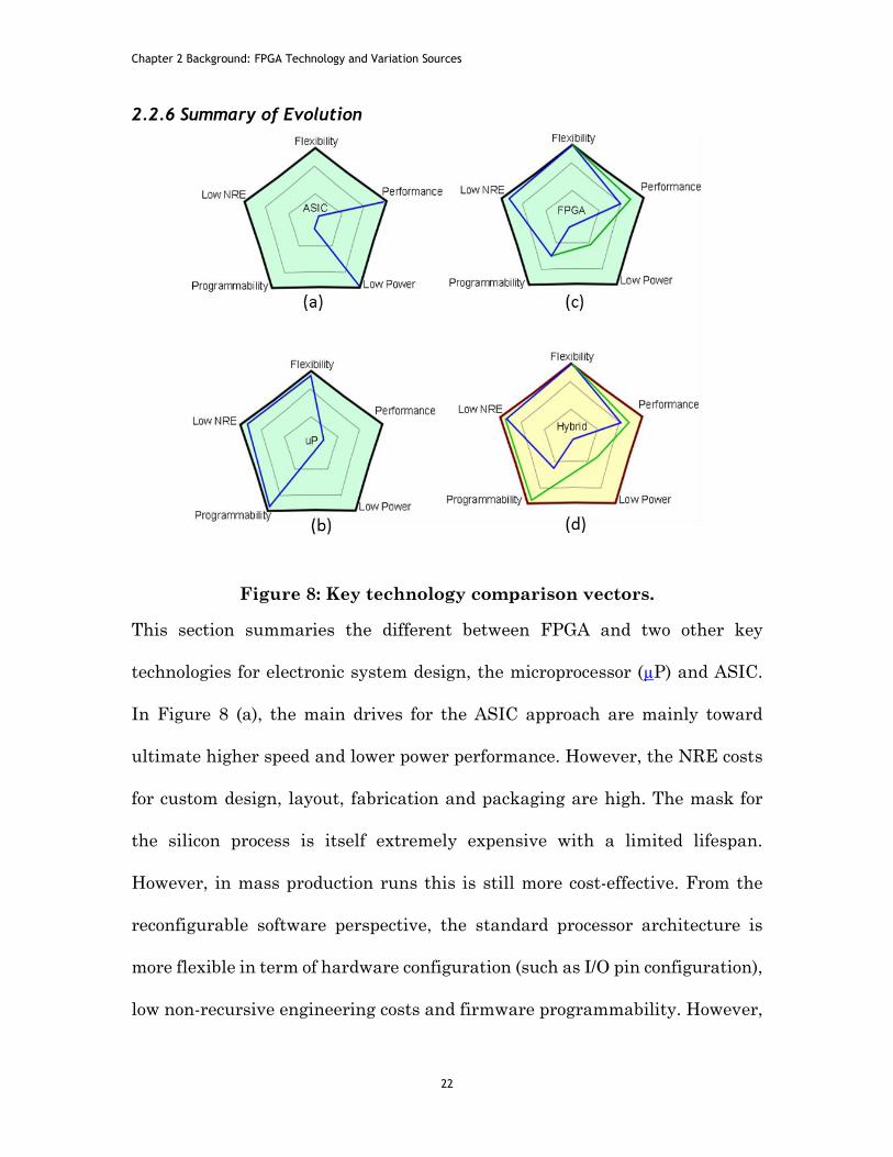
Figure 8: Key technology comparison vectors.
This section summaries the different between FPGA and two other key
technologies for electronic system design, the microprocessor (µP) and ASIC.
In Figure 8 (a), the main drives for the ASIC approach are mainly toward
ultimate higher speed and lower power performance. However, the NRE costs
for custom design, layout, fabrication and packaging are high. The mask for
the silicon process is itself extremely expensive with a limited lifespan.
However, in mass production runs this is still more cost-effective. From the
reconfigurable software perspective, the standard processor architecture is
more flexible in term of hardware configuration (such as I/O pin configuration),
low non-recursive engineering costs and firmware programmability. However,

Chapter 2 Background: FPGA Technology and Variation Sources
23
the downsides are that it is high in operating system overheads and compiler
inefficiency, and there may also be a performance reduction due to the indirect
relationship between the hardware and the software on the processor [18], as
shown in Figure 8 (b).
Programmable devices or the FPGA architecture fit in between the other two
design approaches and offer the greatest hardware configuration flexibility
and higher performance compared to general processor approaches as well as
lower NRE costs compared to the ASIC. In recent and past decade, advances
in research and on the FPGA has been largely focused on improving the speed
performance and optimising power consumption, as illustrated in the green
line in Figure 8 (c). Given the benefit for both application-specificity and
flexibility in a larger system, modern FPGAs are now also blending more and
more application-specific hard-blocks with their traditional soft-fabric forming
new hybrid architectures. The motivation for and benefit from the hybrid
structures are also illustrated in the green line in the yellow pentagon at the
bottom left of Figure 8 (d).
2.2.7 Fundamental Structure of the FPGA
This section explains the underlying building block of the FPGA soft-fabric
architecture and the terms associates with it from the most basic primary
elements to the hierarchy which is build up.

Chapter 2 Background: FPGA Technology and Variation Sources
24
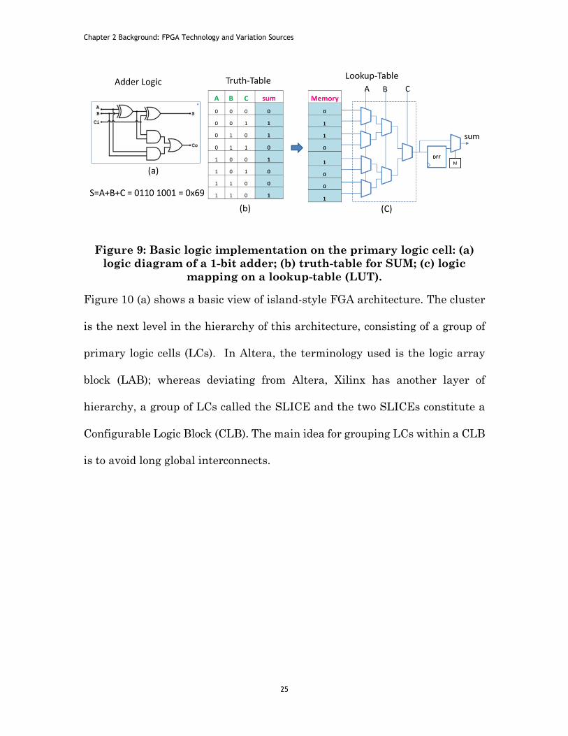
2.2.8 Logic Block
The basic building block in a FPGA comprises a lookup-table (LUT), a register
(DFF) and a multiplexer (MUX), as shown in Figure 10(c). It is normally called
a logic cell (LC) in Xilinx, while the equivalent from Altera is called the logic
element (LE). For ease of explanation, Xilinx’s terms will mainly be used in
this thesis. Figure 9 demonstrates the primary concept of a simple logic
implementation on a FPGA. This example demonstrates the implementation
of basic logic circuit of a single bit adder in Figure 9 (a). The truth-table is first
derived (Figure 9 (b)), this process is normally supported using a synthesis
CAD tools. The synthesis processes basically computes each value of the logical
expression of the circuit according to their functional arguments. In this
example, the expression of sum = A + B+ C = 0x69 is stored in the k-input size
lookup-table or K-LUT as shown in Figure 9 (c). The memory size of the LUT
is defined as 2𝑘 bits or 8 in this case for K = 3. Although the 4-LUT was once
the more common structure, traditionally introduced because of area efficiency,
it should be noted that modern FPGA structures are already built-in with 5 to
7 LUTs for better speed performance.
Chapter 2 Background: FPGA Technology and Variation Sources
25
Figure 9: Basic logic implementation on the primary logic cell: (a)
logic diagram of a 1-bit adder; (b) truth-table for SUM; (c) logic
mapping on a lookup-table (LUT).
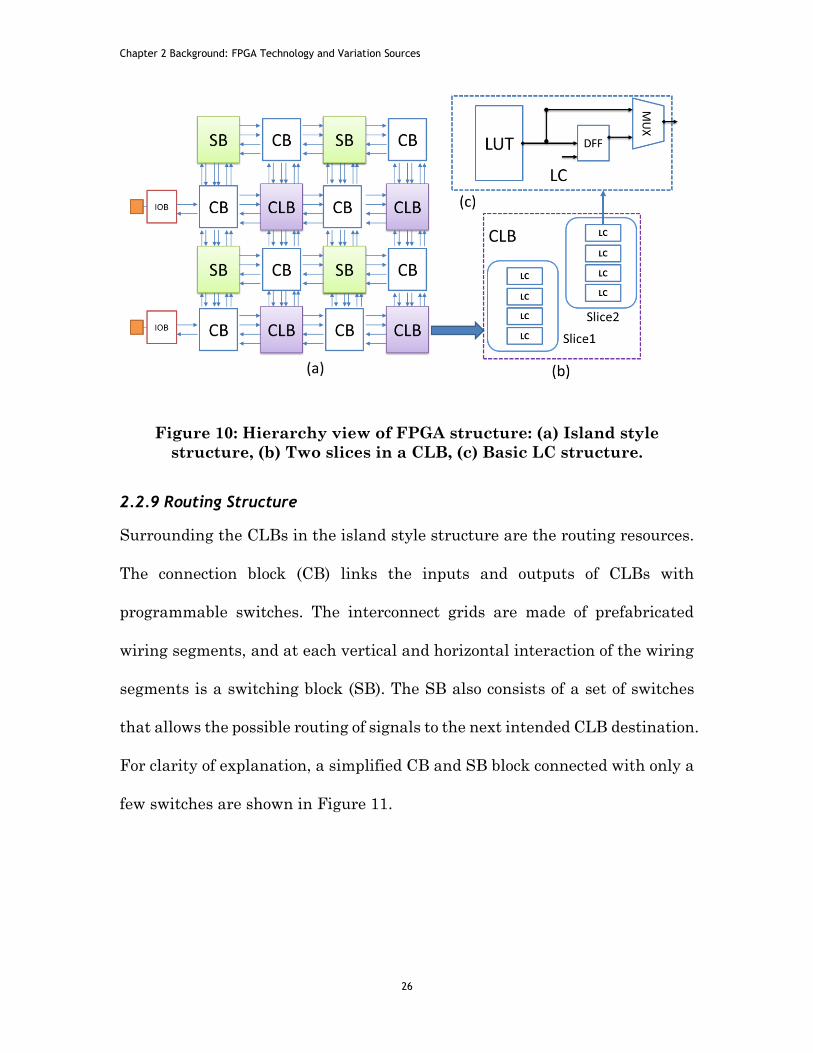
Figure 10 (a) shows a basic view of island-style FGA architecture. The cluster
is the next level in the hierarchy of this architecture, consisting of a group of
primary logic cells (LCs). In Altera, the terminology used is the logic array
block (LAB); whereas deviating from Altera, Xilinx has another layer of
hierarchy, a group of LCs called the SLICE and the two SLICEs constitute a
Configurable Logic Block (CLB). The main idea for grouping LCs within a CLB
is to avoid long global interconnects.
Chapter 2 Background: FPGA Technology and Variation Sources
26
Figure 10: Hierarchy view of FPGA structure: (a) Island style
structure, (b) Two slices in a CLB, (c) Basic LC structure.
2.2.9 Routing Structure
Surrounding the CLBs in the island style structure are the routing resources.
The connection block (CB) links the inputs and outputs of CLBs with
programmable switches. The interconnect grids are made of prefabricated
wiring segments, and at each vertical and horizontal interaction of the wiring
segments is a switching block (SB). The SB also consists of a set of switches
that allows the possible routing of signals to the next intended CLB destination.
For clarity of explanation, a simplified CB and SB block connected with only a
few switches are shown in Figure 11.

Chapter 2 Background: FPGA Technology and Variation Sources
27
Figure 11: Routing resources structure.
2.3 Introduction to Variation
Variations have become more dominant with the continued scaling of the
CMOS process. The complexity has increased, resulting in higher fabrication
costs to achieve uniformity in die production. This limitation can result in
random and spatially varying deviations from intended design parameters,
and affecting speed, power and reliability. Conservative approaches to increase
the operating timing margin across the whole chip to reduce the impact of
parametric yield are imprudent and reduce performance, especially when the
consideration is based on worst-case scenarios.
In addition to the physical parameter variation, dynamic environmental
sources of variation such as temperature, or supply voltage changes during
operation require engineers to employ more aggressive techniques. Similar to

Chapter 2 Background: FPGA Technology and Variation Sources
28
all other CMOS devices, FPGAs are no exception. In fact, the impact of
variation could be more severe compared to ASICs, because the circuit
mapping and critical path routing processes may result in any combination of
worst and best case variability path or regions. This section provides a general
description of sources of variation and discusses its impact on FPGA technology.
Finally published variation tolerance techniques are reviewed.
2.4 Classification of Variability
Sources of variation can be classified into two main categories. First, the
imperfection during manufacturing and second operational environmental
changes, degradation over time due to ageing and wear-out can all be broadly
categorised as either spatial or temporal variations [19]. Figure 12 clarifies the
classification of variation based mainly on timeline since the devices was
manufactured. For spatial variation, the time assumption is constant (t=0s),
and the changes of devices in the characteristics over time are therefore
considered temporal (t = t’).
Chapter 2 Background: FPGA Technology and Variation Sources
29
Figure 12: Spatial and temporal variation classification.
a) Process variation or the spatial variation mainly involves imperfection
during the manufacturing process resulting in parametric deviation of
transistor value between different die (inter-die) as well as variation
within a same die (within-die/ Intra-die). Inter-die variation is a
systematic type of variation which generally shows spatial correlation
behaviour and normally results from varying MOS transistor
dimensions in length or width (L/W), oxide thickness (TOX), and flat-
band condition [20] whereas line-edge-roughness (LER) or random-
dopant fluctuations (RDFs) cause within-die variation with stochastic
characteristic [21].
b) Temporal variation, on another hand is due to changes in the
characteristics of a device over its lifetime. Temporal variations can also
be divided into two main branches, which are environmental and ageing,

Chapter 2 Background: FPGA Technology and Variation Sources
30
where voltage and temperature variations can be classified as
environmental.
c) Negative and positive bias-temperature instability (NBTI & PBTI), hot-
carried-injection (HCI), time dependent dielectric breakdown (TDDB),
and electromigration all fall into the Ageing category [22, 23].
2.5 Process Variation Sources
Figure 13 gives a summary of the key factors in process variations, which can
be either systematic or statistical. Systematic variations are caused by
imperfection in the mask and optical tooling mechanism and result in
repetitive offset from chip-to-chip. Systematic variability is deterministic, and
therefore can be estimated and improved using specific design techniques;
however intrinsic variations are statistical and thus the impact cannot be
reduced through improvements in the manufacturing process [24]. The
following briefly explains and classifies them into two main categories of
tooling-related and intrinsic variation.
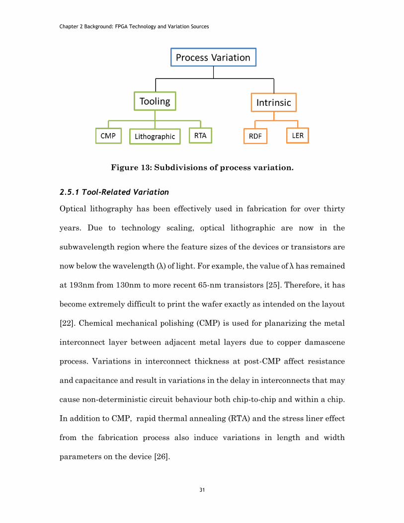
Chapter 2 Background: FPGA Technology and Variation Sources
31
Figure 13: Subdivisions of process variation.
2.5.1 Tool-Related Variation
Optical lithography has been effectively used in fabrication for over thirty
years. Due to technology scaling, optical lithographic are now in the
subwavelength region where the feature sizes of the devices or transistors are
now below the wavelength (λ) of light. For example, the value of λ has remained
at 193nm from 130nm to more recent 65-nm transistors [25]. Therefore, it has
become extremely difficult to print the wafer exactly as intended on the layout
[22]. Chemical mechanical polishing (CMP) is used for planarizing the metal
interconnect layer between adjacent metal layers due to copper damascene
process. Variations in interconnect thickness at post-CMP affect resistance
and capacitance and result in variations in the delay in interconnects that may
cause non-deterministic circuit behaviour both chip-to-chip and within a chip.
In addition to CMP, rapid thermal annealing (RTA) and the stress liner effect
from the fabrication process also induce variations in length and width
parameters on the device [26].
Chapter 2 Background: FPGA Technology and Variation Sources
32
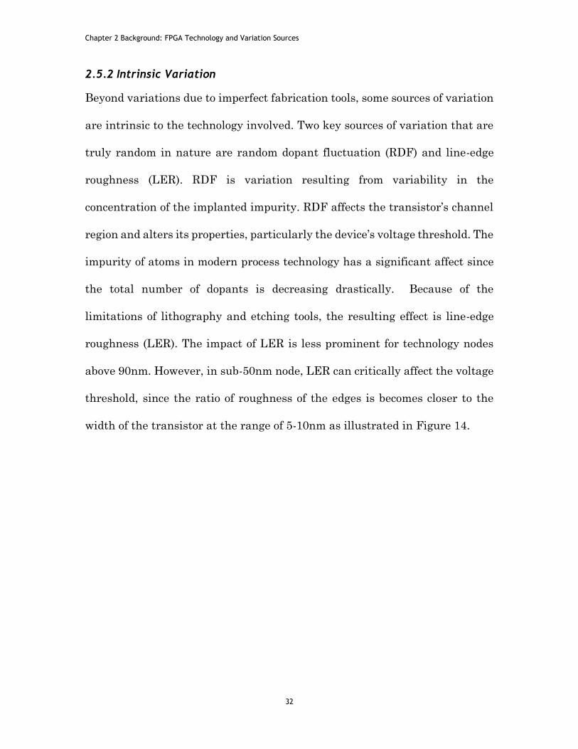
2.5.2 Intrinsic Variation
Beyond variations due to imperfect fabrication tools, some sources of variation
are intrinsic to the technology involved. Two key sources of variation that are
truly random in nature are random dopant fluctuation (RDF) and line-edge
roughness (LER). RDF is variation resulting from variability in the
concentration of the implanted impurity. RDF affects the transistor’s channel
region and alters its properties, particularly the device’s voltage threshold. The
impurity of atoms in modern process technology has a significant affect since
the total number of dopants is decreasing drastically. Because of the
limitations of lithography and etching tools, the resulting effect is line-edge
roughness (LER). The impact of LER is less prominent for technology nodes
above 90nm. However, in sub-50nm node, LER can critically affect the voltage
threshold, since the ratio of roughness of the edges is becomes closer to the
width of the transistor at the range of 5-10nm as illustrated in Figure 14.

Chapter 2 Background: FPGA Technology and Variation Sources
33
Figure 14: Line edge roughness at 90nm and 22nm technology [23].
2.6 Environmental Variation
Temperature and supply voltage variations are categorised as environmental.
The performance of devices is strongly dictated by these conditions.
Figure 15: Classification of sources of environmental variation.
2.6.1 Temperature Variation
Several factors in addition to the ambient temperature affect the rise and
dissipation of temperature within a chip. Regions of the chip with high activity
and power consumption are normally associated with rises in temperature, or
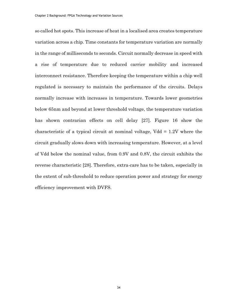
Chapter 2 Background: FPGA Technology and Variation Sources
34
so called hot spots. This increase of heat in a localised area creates temperature
variation across a chip. Time constants for temperature variation are normally
in the range of milliseconds to seconds. Circuit normally decrease in speed with
a rise of temperature due to reduced carrier mobility and increased
interconnect resistance. Therefore keeping the temperature within a chip well
regulated is necessary to maintain the performance of the circuits. Delays
normally increase with increases in temperature. Towards lower geometries
below 65nm and beyond at lower threshold voltage, the temperature variation
has shown contrarian effects on cell delay [27]. Figure 16 show the
characteristic of a typical circuit at nominal voltage, Vdd = 1.2V where the
circuit gradually slows down with increasing temperature. However, at a level
of Vdd below the nominal value, from 0.9V and 0.8V, the circuit exhibits the
reverse characteristic [28]. Therefore, extra-care has to be taken, especially in
the extent of sub-threshold to reduce operation power and strategy for energy
efficiency improvement with DVFS.

Chapter 2 Background: FPGA Technology and Variation Sources
35
Figure 16: Inverse path delay characteristics at lower voltage level
with increase in temperature [29].
Several factors that affect the temperature variation are listed as follow[23]:
o Neighbouring blocks power characteristic of the circuit switching
activities and capacitive load around the location or within the
same region will affect power consumption and heat generation.
o The thermal conductivity of material is closely related to power
density. Heat generated in bulk CMOS device is dissipated
through both the silicon substrate and the interconnecting wires.
In SOIC (silicon-insulator) technology, however, heat dissipation
occurs mainly along the wires and results in rapid heat increases
in regions that consume a lot of energy. This disparity results in
greater temperature gradients between hot and cold regions
within a chip.

Chapter 2 Background: FPGA Technology and Variation Sources
36
o Cooling efficiency of the packing or heat sink helps to improve
the thermal profile. However, this issue exacerbated in the 3D
(three-dimensional) stacking technology where circuits are
sandwiched together. This means that it becomes more
challenging to dissipate heat.
o Switching activity or the workload running on the system in a
location or core can drastically increase the temperature in a
specific region especially over a long period. In modern multi-core
processor system or reconfigurable systems such as the FPGA,
the workload may be distributed or inter-swap over time. This is
however largely depending on the ability of the underlying
support resources of the architecture for dynamic or partially
dynamic reconfiguration. The strategy of periodically relocating
the workload to different regions or cores will vary the thermal
profile over time.
2.6.2 Supply Voltage Variation
Supply voltage variations mainly result from voltage drop across resistive
interconnect (IR-drop) and inductive (or di/dt) noise. The power distribution
grid within a chip come with its inheriting parasitic resistance, and when a
steady state current flows through, this cause IR-drop which can be derived
from the basic Ohm’s Law as ∆𝑉𝐼𝑅 = 𝑅𝑔𝑟𝑖𝑑 ∗ 𝑖(𝑡) . Meanwhile, fluctuations of

Chapter 2 Background: FPGA Technology and Variation Sources
37
voltage due to the parasitic inductance, commonly referred to as the di/dt noise,
(∆𝑉𝑑𝑖
𝑑𝑡
= 𝐿𝑝𝑎𝑟𝑎𝑠𝑖𝑡𝑖𝑐 ∗𝑑𝑖
𝑑𝑡). These rapidly changing power noise effects normally
have time constants in the range from nanoseconds to microseconds [29]. In
summary, the characteristics of the circuit depend significantly on the
operating voltage level. A drop of supply voltage affects both the grain and gate
bias and the impact is reduced in a flow of current. One profound impact of this
on circuit operation is that it does not just increase the delay in the critical
path, but may make those near-critical paths that have not been optimised
become critical.
Energy harvesting system that tends to provide variable power levels can also
be considered as environmental variation. With the expansion of wireless
sensor networks and looking toward to the wider scope of the Internet-of-
Things (IoT), it is becoming more important to prolong and support existing
battery-powered system [7, 30]. In certain applications, energy harvesters have
completely replaced traditional batteries. Examples of commercial applications
are the battery-less (infrared remote control) and (wireless wall switch) [31].
Energy harvester devices tend to provide dynamic power, and voltage levels
may vary at run-time. The strategy to allow circuit working in wider operating
range is therefore intentional [32-34]. The rationale for this kind of circuit is
that energy should be used while it is abundant, which means that circuit can
run at their optimum speeds. This is because the process of energy conversion
and storing incurs extra circuit complexity that reduces its efficiency. The
Chapter 2 Background: FPGA Technology and Variation Sources
38
benefits of this kind of system able to operate under a wide range of operational
voltage levels is maintaining circuit functional or at least part of the core
features at a reduces rate while energy is scare and low [35-38].
2.7 Temporal Variation – Ageing Related
While environmental temporal variation such as changes in temperature and
voltage add to the circuit marginalities, ageing-related temporal variation
affects circuit performance gradually over a period. Key mechanisms
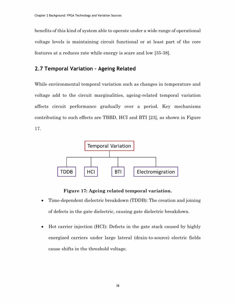
contributing to such effects are TBBD, HCI and BTI [23], as shown in Figure
17.
Figure 17: Ageing related temporal variation.
Time-dependent dielectric breakdown (TDDB): The creation and joining
of defects in the gate dielectric, causing gate dielectric breakdown.
Hot carrier injection (HCI): Defects in the gate stack caused by highly
energized carriers under large lateral (drain-to-source) electric fields
cause shifts in the threshold voltage.
Chapter 2 Background: FPGA Technology and Variation Sources
39
Bias-temperature instability (BTI): The Capturing of holes (electrons)
from the inverted channel in PFETs and NFETs by broken Si–H bonds,
such as charge-trapping sites in high-K gate dielectrics (HfO2).
Electromigration: is the transport of material caused by the gradual
movement of the ions in a conductor due to the momentum transfer
between conducting electrons and diffusing metal atoms.
2.8 Sensing and Characterisation
Sensing circuits play an important role in understanding and characterising
the variability profiles of a particular batch or individual chip. The primary
function of sensing circuits is twofold. First, to quantify between the deviated
characteristic of a device and its ideal intended behaviour. Secondly, the on-
chip sensing circuits can be used for continued health monitoring to help
provide adaptive refitting for environmental changes and temporal
degradation. Less conservative guard banding can be achieved with the
availability of characterisation information, which can mean timing yield
improvements. Furthermore, with accurate sensing and characterisation, a
detailed variation map can be generated. Utilising such information a
controller can supplement the power of weakening regions and critical paths
can be diverted. Therefore potential run-time malfunctions can be avoided.
This section looks at several frequently used sensing and characterisation
techniques that can be applied to ASIC and FPGA design.

Chapter 2 Background: FPGA Technology and Variation Sources
40
2.8.1 Off-chip Sensing
Off-line sensing is a non-intrusive approach of characterisation without built-
in sensors; external measurements equipment is used instead. The most
straightforward characterisation technique traditionally used is to incorporate
extra test pads for direct access of test probes that are able to inject stimulus
signals containing multiple electrical parameters to the sections of the circuits
[39]. Accurate current and voltage characteristics of the device can be obtained
with this measure. However, such an approach is expensive with the number
of test pads required especially with large circuit, the area overhead makes
this not viable. Although, area optimisation techniques such as multiplexing
the circuit in the array matrix format is possible [40], yet precision and complex
analogue voltage-current measurement setup may still be needed. For modern
multi millions gates FPGAs, this characterisation technique is almost
impossible.
Optical imaging is another attractive non-invasive approach for chip
variability characterisation without the need of embedded hard sensors. This
technique is based on measurements of the deflective of the electromagnetic
wave from the emitting source such as infrared to provide visual
representation of the study. In [41], the optical imaging technique was
successfully demonstrated to map systematic and random variability effect of
microprocessor chip in 65nm technology. Static imaging camera was utilised
in this approach to capture the light emission from off-state leakage current
Chapter 2 Background: FPGA Technology and Variation Sources
41
(LEOSLC). The authors suggest the recorded data that can be easily correlated
to produce variation map and be successfully adapted for the evaluation and
enhancement of the fabrication process as well as to develop countermeasure
for the possible reliability issues.
Thermal and power characterisation using infrared imaging technique applied
on FPGA is recently presented in [42]. In this work, run-time thermal
characterisation is performed by capturing the emissions from the back of the
chip. The result is the visualisation of operational thermal gradient and hot
spot for the particular application mapped on FPGAs. Again, these off-chip
techniques are attractive but require complex measurement equipment and
procedures. In addition, due to the data being gathered externally, this makes
the variation map correlation process less straightforward.
2.8.2 On-chip Sensing
An alternative to the off-chip sensing are built-in hard sensors. The state of
the art of multicore processors is normally equipped with multiple thermal
sensors. Accurate sensing requires fine granularity of build-in sensors that is
scattered across the chip and the question for the research has always been at
what cost or overhead.
Sensing and characterisation based on Ring oscillator (RO) was presented in
the past and recent years due to its simplicity in implementation either on-line
or off-line [3, 43-49] . In [43], authors utilised the method to measure random

Chapter 2 Background: FPGA Technology and Variation Sources
42
variations in MOSFET threshold voltages. Die-to-die variability
measurements with ROs that is sensitive to parameter was proposed in [44].
In [46], authors proposed to create Path-based RO to measure and monitor the
targeted critical path under process variation. RO was also presented as a
temperature sensor as an alternative to analog sensing circuits. RO circuits
may be convenient to deploy, yet this approach may increase the overall area
of the circuit. In addition, the circuit itself is reactive to temperature and
voltage fluctuation. The RO method unfortunately has also been remarked as
a bad instrumentation technique for FPGA variability as it does not accurately
represent the circuit path in FPGA designs. At high frequency oscillation, RO
circuit itself generates heat, this consequently adds extra complexity and
variability to the situation [50].
Increasing technology scaling in nanometer regions results in local random
transistor parameter variations. The effects of such phenomena as random
dopant fluctuations (RDF) and line edge roughness (LER) can dominate
mismatch in neighbouring devices. Particularly in SRAM cells with high
circuit density, mismatch can deteriorate the circuit functionality greatly.
Current latch sense-amplifier (CLSA) for example in [51] is proposed to
measure mismatch between two transistors. Since only a pair of transistors
can be measured at any one time, this limits its usefulness. Extension from the
basic mismatch sensor, array based characterisation is also presented in [52,
53]. Yet, the limitation of this method has been the low sensitivity due to device

Chapter 2 Background: FPGA Technology and Variation Sources
43
properties changing linearly with voltage threshold variation when the device-
under-test (DUT) is biased in the saturation region.
2.8.3 Soft Sensing in FPGA
Reconfigurable architectures such as FPGA give a unique opportunity for
sensing and mitigating the effects of the variability using the generic built-in
flexible resources rather the dedicated embedded sensing circuits. This is
called “soft sensing” in this thesis. Modern FPGA architecture such as Altera’s
Stratix family and Xilinx’s Virtex series are all equipped with a thermal sensor.
However, a single sensor cannot sufficiently provide the temperature gradient
of the chip. Never mind the ability to identify the maximum value or hot spots
of the chip.
Ring oscillator (RO) is a commonly used technique due to its simplicity in
implementation either on-line or off-line. Off-line RO is normally used for
characterisation purposes such as variability of delay with the changes of
temperatures [54]. Authors of [47, 54] proposed one of the earliest thermal soft
sensing approach on reconfigurable computing architecture. Flexible RO-based
thermal sensing replaced conventionally used analog sensor and its complex
control circuit. Example of works in [3, 55] also used RO, instead of thermal,
authors perform characterisation of FPGA process variation effect by
measuring its component delay.
Chapter 2 Background: FPGA Technology and Variation Sources
44
On the other hand, to continuously monitor the health and provide adaptations
to temporal effects [45, 46, 56], on-line soft sensing techniques can be beneficial.
In [57], thermal soft sensing technique is proposed. This approach utilise an
adder-accumulator multiplier to make the computation without the need of RO.
Wong et al. [58-60] proposed novel characterisation techniques that enables
accurate combinatorial delay measurement. This differs from the previous
mentioned methods that used RO for latency measurement [3]. This work
performs characterisation by stepping the system frequency gradually for error
detection.
Leveraging the unique reconfigure structure of FPGA, extra-embedded
analogue sensors can be avoided for PVT (process, voltage and temperature)
characterisation. And this forms sound of the foundations for the work
presented in this thesis. Furthermore, due the final application to be
implemented on the FPGA is not known until it is fabricated, it is hard to
predict where and how sensors should be distributed across the chip evenly.
Therefore, soft sensing grants additional advantages for monitoring circuits,
particularly in the use of on-chip hot spot tracking.
2.9 Conventional Variation Tolerance in FPGAs
2.9.1 STA and SSTA
In Static Timing Analysis (STA), timing analysis is carried out in input
independent manner, and purpose to determine the worst-case delay or critical

Chapter 2 Background: FPGA Technology and Variation Sources
45
path of the circuit over all possible input combinations. Therefore, STA
approach often gives pessimistic timing estimation. Hence, this reduces the
speed performance that could otherwise be much faster. Extensions of the STA
are corner analysis, where worst-case and best-case scenarios for PVT
variation can be presented. The best cases are defined as fastest processes at
highest voltage level operating at the lowest temperature, and the worst case
will be the opposite with a slow process at the lowest voltage and highest
temperature. Examples of the effect of PVT on path delay are shown in Figure
18
Figure 18: Corner analysis with STA tools
Despite the conservative timing estimation on the critical paths, STA is not
able to accurately model intrinsic variability that is random and stochastic.
Under random parametric fluctuations, the shorter paths or near-critical paths
that have not been optimised have the tendency to become critical.
Statistical static timing analysis (SSTA) tools aim to identify these statistically
critical paths and minimize the chances of these paths becoming critical.
However, the drawbacks of SSTA tools include the uniform strategies used
Chapter 2 Background: FPGA Technology and Variation Sources
46
across the whole chip and between different dies. Therefore, accurately
modelling statistical variation from one die to another requires an accurate
variation model value of mean (µ) and standard deviation (σ). Also it is
becoming difficult to produce statistical models for the larger systems with
high random variation that are expected in future node technology, making the
characterisation cost un-scalable to deal with the complexity of a system with
increasing numbers of statistically critical paths [61].
2.9.2 Optimisation of Structural Parameters
Structural parameter optimization is another proposed approach for
mitigating FPGA variation, which focuses on traditional architectural
parameters such as varying the value of N, the number of LUTs per CLB, and
K, the number of inputs to a LUT [62]. However, study in [63] shows that
varying the value of N and K value does not provide significant improvements
over the variation concern [23].
2.9.3 Transistor Sizing
Transistor sizing can be used in ASICs to optimize path delay and power
performance. However, the process of transistor sizing for its width and length
(W/L) at layout level for FPGAs requires a huge effort and will consumes
significant amount of engineering time. Research into automated transistor
sizing on FPGAs for area and speed trade-off [64] is also promising in exploring
the use transistor sizing to mitigate the effect of variability on FPGA

Chapter 2 Background: FPGA Technology and Variation Sources
47
architecture. Yet, this technique is computational expansive and the
variability-critical paths (VCPs) cannot easily predefined.
A recent project named the Programmable Analogue and Digital Array
(PAnDA) architecture [24] represents a new approach to intrinsic variability,
introducing reconfigurable transistor arrays at the analogue level. This
approach allows low-level optimization during the post-fabrication stage and
results in the recovery of the loss of performance yield introduced by stochastic
variability. However, the extra configurability of the architecture also comes
with a high area overhead.
2.9.4 Asynchronous Techniques
Asynchronous designs are highly adaptive to changes in voltage and delay,
providing robustness depending on the delay assumptions that are made [65].
The most robust class is delay-insensitive (DI), where circuits will operate
correctly without any assumption of delay in either gates or wires. Circuits
with carefully identified delay assumptions on isochronic wire are called quasi-
delay-insensitive (QDI) [66] or speed independent (SI) [67]. These circuits
consider only the gate delay and neglect wire delay when ensuring circuit
correctness.
There are many approaches or protocols for implementing asynchronous
circuits. A taxonomy of potential protocol implementations is summarized in
[65]. The choice of an asynchronous communication protocol affects the

Chapter 2 Background: FPGA Technology and Variation Sources
48
characteristics of circuit in term of implementation power, area, throughput
and robustness.
In the past decade, different asynchronous FPGA architectures have been
presented motivated mainly by the pursuit of low power and/or high-speed
performance. These architectures can be classified into two main styles. The
first relies heavily on timing assumptions to guarantee the correctness of the
logic, and the second alters the traditional architecture at fine-grained level
with the intensive use of state-holding memory components (such as C-
elements), which implies significant overheads in size and power [68, 69].
Details of asynchronous FPGA (AFPGA) designs are reviewed in Chapter 3.
2.10 Variation Aware and Late Binding Techniques
Process variation has become a hot issue with the continue technology scaling.
The major challenges are to resolve reliability issues while maintaining yields.
Unique functional configurability of FPGA provide extra-flexibility to mitigate
problems such as variation aware techniques that leverage the knowledge of
how each chip are affected by the variation. With the assumption of mature
off-line and online sensing techniques, each chip can be characterised and treat
differently using late binding techniques such as multiple-reconfiguration,
region relocation, and path reconfiguration. Compare to conservative worst-
case timing assumption approach the variation-aware approach are promising
for better circuit performance.
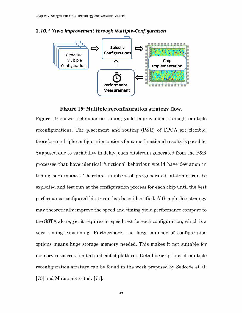
Chapter 2 Background: FPGA Technology and Variation Sources
49
2.10.1 Yield Improvement through Multiple-Configuration
Figure 19: Multiple reconfiguration strategy flow.
Figure 19 shows technique for timing yield improvement through multiple
reconfigurations. The placement and routing (P&R) of FPGA are flexible,
therefore multiple configuration options for same functional results is possible.
Supposed due to variability in delay, each bitstream generated from the P&R
processes that have identical functional behaviour would have deviation in
timing performance. Therefore, numbers of pre-generated bitstream can be
exploited and test run at the configuration process for each chip until the best
performance configured bitstream has been identified. Although this strategy
may theoretically improve the speed and timing yield performance compare to
the SSTA alone, yet it requires at-speed test for each configuration, which is a
very timing consuming. Furthermore, the large number of configuration
options means huge storage memory needed. This makes it not suitable for
memory resources limited embedded platform. Detail descriptions of multiple
reconfiguration strategy can be found in the work proposed by Sedcode et al.
[70] and Matsumoto et al. [71].

Chapter 2 Background: FPGA Technology and Variation Sources
50
2.10.2 Variation Aware Modelling
There have been several attempts at improving FPGA timing yield by
providing statistical analysis and process variation modelling for variation
aware placement and routing [70, 72-77] . Another example in [73] provides
variation aware timing-driven algorithm to optimise timing statistically and
maximize timing yield. Simulation result based on statistical enhance versatile
place and route (VPR) tools [78] show 3.4x increase in yield with guard-banding
and 25x with speed-binning using the variation aware placement techniques.
However, the guard-banding and speed-binning techniques may not be
sufficient with the presence of within-die variation. This is because the chip
performance will be greatly degraded with the wide banding, removing the part
of the incentive for technology scaling in the first place.

Chapter 2 Background: FPGA Technology and Variation Sources
51
Figure 20: Variation aware chipwise placement design flow [72].
One of the earliest variation aware placement for FPGA is proposed by authors
in [72], the design flow is shows as in Figure 20. The authors suggest with the
help of the software model that have been developed within the VPR
framework [78]. Worthwhileness of variation ware placement is first evaluated
for performance gain can be expected. Simulation result shows up to 19.3%
performance improvement can be achieved with chipwise placement. Part of
this thesis is also based on the assumption that a variation map is obtainable.
In nanometer process technology, variation in FPGA has shown both
correlated and random effects. Authors in [75] proposed an improvement model
that consider both inter-die and intra-die variability including the delay
variability in routing resources. The purposed model also enhanced with
statistical timing analysis, supported by variability aware P&R based on VPR
framework.

Chapter 2 Background: FPGA Technology and Variation Sources
52
2.10.3 Relocation, Remapping and Rerouting
Figure 21: (a) Region relocation, (b) Path reconfiguration.
The idea of region relocation is similar to the strategy used in wear levelling
for managing and prolonging the lifespan of traditional flash memory that
have limited write cycles due to wear out. The wear levelling technique uses
algorithms that track the frequency each location has been written and works
to distribute data evenly across each memory block of the entire flash drive.
This process decreases the total wear on the drive, thereby increasing the
lifespan of the drive. A similar concept applies to the region relocation where
the FPGA are partitioned into regions and circuit can be configured into the
allocated regions. As a region with configuration ages, the circuits can be
swapped to a region that has not been assigned before. This wear-levelling
technique is particularly useful for the extending lifetime of the FPGA as well
as improving its reliability [79].

Chapter 2 Background: FPGA Technology and Variation Sources
53
Srinivasan et al. [80] suggest the relocation of circuit over time with the unused
region of the FPGA to reduce the effect of HCI. Figure 21 (a) illustrates the
regions swapping strategy between high switching activities and the less active
region to minimised the age acceleration effect of HCI. Also with the
assumption of enough modular level of the available regions, partial dynamic-
reconfiguration can also be supported. Contrast with the multiple
reconfiguration techniques, there is no need for generation of multiple
bitstream/netlist, therefore huge storage space requirement can be avoided
[70]. Yet, the challenges with this approach are strategically circuit
partitioning into sub modules and then the support for reassembling them.
Figure 21 (b) shows the path reconfiguration strategy to improve timing yield
in FPGAs compensating for variability by re-mapping and re-placement
[81].This work exploit the flexibility of LUTs mapping and presented a
software tool that can systematically compute all the possible way for a given
logic network. The experiment results show mean and variance of a critical
path delay can be reduced similar to using the statistical Monte Carlo
simulation techniques.
2.11 Summary
Variability issues in sub-nanometer CMOS technology have appeared as a
critical challenge to the ability to deliver a design that meet all the timing,
power and reliability specification. With the continuous scaling of the

Chapter 2 Background: FPGA Technology and Variation Sources
54
technologies and increasing power density, the pressure to deliver the design
within the time frame while dealing with the variability issues is going to get
worse. The two main variability challenges are, first the static variability due
to process scaling and limitation of lithography and etching tools. The
imperfection during of manufacturing process results in parametric or spatial
variability for inter-die and intra-die. Secondly the environmental changes
and temporal ageing variability is dynamic changes after deployment.
Tackling the dynamic variability such voltage changes due to increasing
workload and temperature during operation is relatively more challenging.
Traditional techniques that apply excessive operating margin across the whole
chip based on worst-case scenario reduced system efficiency. This thesis aims
to explore the practical variation tolerance strategies without scarifying the
system efficient that relies on worst-case guard-banding.
In advanced technology nodes, a design with multiple billion atomic-scale
transistors; the assumption that not all of the transistor will work or some will
fail at the later life of the device may not be unfair. FPGA architecture has
been the centre of this work because its inherit reconfigurability nature that
provides unique opportunities to cope with these static and dynamic variability
challenges. For example, rerouting and remapping to achieved thermal and
wear-out balance.
The cornerstone for adaptively to changes is the ability to measure and
quantified the variability profile of a specific chip as well as to track the

Chapter 2 Background: FPGA Technology and Variation Sources
55
changes during operation. The characterization can be performed either with
off-chip or on-chip sensing. The result is chip variability profiles or variation
maps.
Off-chip sensing offers a non-intrusive characterization – for example, optical
and infrared imaging techniques. However, the downside being costly and
complex equipment needed. Also, it’s less intuitive to correlate data collected
externally with the operation activities. On the other hand, the on-chip sensor
allows continue monitoring the health of the chip. Yet, the major challenges
for on-chip sensing are the distribution of the sensors and reduced chip density
due to the area occupied by the sensors. The alternative to the on-chip and off-
chip sensor is soft-sensing. This technique is unique only to FPGA. Soft-
sensing in this thesis context exploits the generic built-in resources of the
FPGA replacing the conventional analogue sensor. For example, the ring
oscillator can be temporally configured across the FPGA fabric evenly and
characterise its thermal profile for “pre” and “post” system implementation.
The “pre” implementation thermal profile gives the static variability map of
the chip while the “post” for dynamic thermal gradient results after a fixed
period of operation. In addition, the soft-sensing technique also provides extra
gratification to implement and track variability on targeted area rather, to
widely distribute them across the whole chip. This reduces area overhead.

Chapter 2 Background: FPGA Technology and Variation Sources
56
Various variation tolerant techniques have been proposed, some are unique
only for FPGA and some are common between the FPGA and ASIC. The
summary of the techniques is shown Table 2.
Table 2: Summary of Existing Variation Tolerance Techniques in FPGA
Techniques Remarks
STA Pessimistic timing variation analysis based on worst-case. Reduce performance.
SSTA Less conservative than STA for intra-die variation but still a “One-size-fits-all” approach.
Transistor sizing Time-consuming engineering efforts for over million transistor circuit.
Structural Parameters Optimisation: Do not provide significant improvement for variation concern.
Multiple-configuration Expansive computation at speed test and required huge memory for all possible configurations storage.
Variation-aware Modelling Improve yield over STA and SSTA, however accurate variation map generation is required for inter-die and intra-die variability.
Relocation, Remapping and Rerouting
Improve large storage problem compare to multiple configuration techniques, however, the challenges are system partitioning and regions allocation.
Asynchronous Techniques
Highly adaptive to changes in voltage and timing variability. However, asynchronous circuits are more complex to design and normally incur high handshaking's circuit overhead. Also, traditional FPGA architecture only has limited resources to support Asynchronous implementation.
STA guaranteed correct operation based on worst-case estimation and,
therefore, reduced in possible performance. Whereas, SSTA is less
conservative compared to STA for intra-die variation and the accuracy of the
model relies heavily on the statistical mean and standard deviation values.
The drawback of these approaches is uniform parameter applied across a whole
batch of dies. Yet, this has been a preference strategy for industry thus far
Chapter 2 Background: FPGA Technology and Variation Sources
57
because it is the only practical approach for mass production solution. In
reality, most of the chip in the market can perform much better than the
manufacturer’s conservative specification. The late-binding and variation-
aware techniques for example proven to achieve higher efficiency above
conservative timing specification recommend by the manufacturer.
Above all, the asynchronous technique that is known to be robust to timing
variation and possibility provide an attractive solution. Despite the potential
benefits, asynchronous FPGAs presented in past have not centred on
improving the reliability aspects – rather mainly focus on low power and
throughput performance. Also, to implement asynchronous logic in
synchronous FPGA is proven to be difficult because it’s required manually
manipulate the existing FPGA resources that are designed for the synchronous
system. Introducing asynchronous friendly logic block to traditional FPGA
architecture, therefore, has been the motivations for this work.

Chapter 3: Existing Asynchronous Techniques in FPGA
58
Chapter 3. Existing Asynchronous Techniques in FPGA
3.1 Introduction
This chapter discusses the context of incorporating asynchronous logic into the
programmable logic to tolerate and reduce the negative impact of variability.
The focus of this chapter is divided in two main parts as follow:
Firstly, the principle of asynchronous logic and its potential trade-off is
introduced. Popular delay-insensitive encoding strategies such as 4-phase
dual-rail (4P-DR) and 2-phase dual-rail (2P-DR) are reviewed. Circuit
robustness based on timing assumption made is also classified including speed-
independent (SI) and delay-insensitive (DI) circuits. This section serves as a
basis for further understanding and ease of explanation is the following
chapters.
Second part of the chapter reviews different styles of asynchronous FPGA
architectures presented from the past decade motivated mainly by the pursuit
of either low power and/or high speed performance. These architectures are
classified into four main types for ease of explanation in overview as follow.
Type-1, the architecture that is heavily relies on the timing assumption using
bundle data. Type-2, the architectures that target on high throughput
performance by adopting fine-grain pipelined structures. Type-3, handshaking
based optimisation architecture to improve the coding efficiency in dual-rail

Chapter 3: Existing Asynchronous Techniques in FPGA
59
communication for dynamic power reduction in the communication, and Type-
4, the architecture that combine the benefit of both synchronous and
asynchronous circuit that fit the global asynchronous and locally synchronous
(GALS) paradigm. Other type of asynchronous implementation motivated
different benefits such security advantage also reviews, however this is not the
main focus of this work.
The final section summarise the trade-off of each type of these asynchronous
reconfigurable architectures in the context of its benefits and trade-offs to be
used on a FPGA to mitigate the negative effect of the variability.
3.2 Principles of Asynchronous Design
Digital electronic system designs are predominantly synchronous and
sequential. A sequential circuit is specified by a time sequence of inputs,
outputs and internal states. In synchronous sequential circuits, a change of
internal state occurs in response to synchronous clock pulses [3]. Figure 22
shows a high-level representation of a typical synchronous circuit where the
communication of data is governed by the global clock.
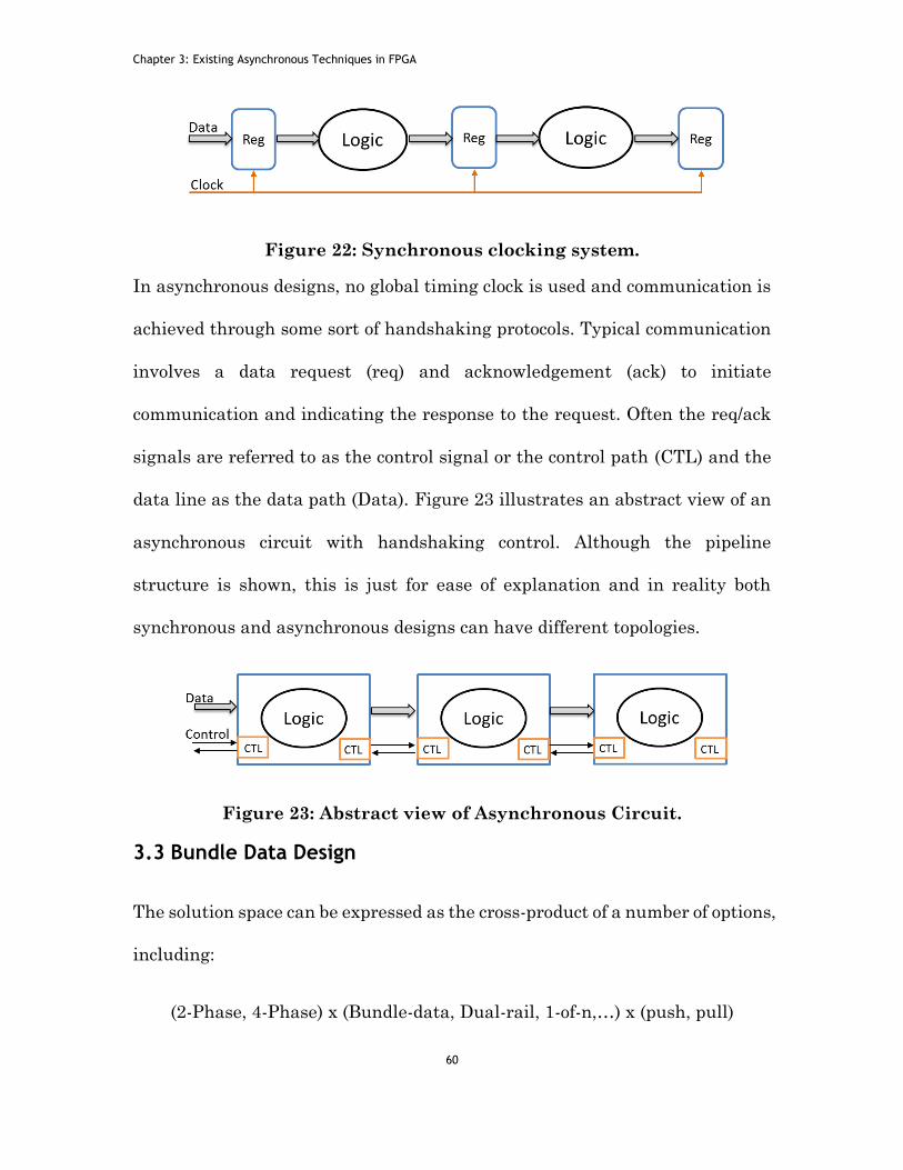
Chapter 3: Existing Asynchronous Techniques in FPGA
60
Figure 22: Synchronous clocking system.
In asynchronous designs, no global timing clock is used and communication is
achieved through some sort of handshaking protocols. Typical communication
involves a data request (req) and acknowledgement (ack) to initiate
communication and indicating the response to the request. Often the req/ack
signals are referred to as the control signal or the control path (CTL) and the
data line as the data path (Data). Figure 23 illustrates an abstract view of an
asynchronous circuit with handshaking control. Although the pipeline
structure is shown, this is just for ease of explanation and in reality both
synchronous and asynchronous designs can have different topologies.
Figure 23: Abstract view of Asynchronous Circuit.
3.3 Bundle Data Design
The solution space can be expressed as the cross-product of a number of options,
including:
(2-Phase, 4-Phase) x (Bundle-data, Dual-rail, 1-of-n,…) x (push, pull)

Chapter 3: Existing Asynchronous Techniques in FPGA
61
The choice of protocol affects the characteristics of the circuit implementation,
such as power, area, speed and robustness. This section explains the
terminology commonly uses in asynchronous circuit design. The most popular
handshaking protocols are discussed, including 2-phase and 4-phase
communication together with dual-rail or bundle-data.
3.3.1 Single-Rail Bundle-Data (SR-BD)
Figure 24: (a) Abstract view of delay matching bundle-data approach;
(b) example of programmable delays bank. (c) AND gate and muxes
fine tune programmable delay [82].
The simplest and most widely used asynchronous protocol is single-rail bundle-
data (SR-BD). The advantages of the SR-BD are its simplicity in design, small
size and ease of validation. An abstract view of the SR-BD approach is shown
in Figure 24 (a). The functional block in this scheme is maintains similar to
the synchronous design and replace the clock line with matched-timing delay
line to indicate the completion of computation or valid data have been received

Chapter 3: Existing Asynchronous Techniques in FPGA
62
using the “done” signal. Hence in many ways the design can easily be migrated
between the synchronous and asynchronous domains by interchanging the
clock line with match delays. Match delay lines are normally fixed and realised
by an inverter chain. However, to deal with the variability, tuneable delay line
has also been proposed. Figure 24 (b) shows an example of a programmable
delay (PD) with a control code for the selectable delay bank. The matching
delay can be either fixed or tuneable. Usually, this type of design cannot be
fine-tuned. The headroom in the non-fine-tuned matching delay means that
the circuit may not operate at its optimum speed. Another example of PD
implementation shown in Figure 24 (c) allows more accurate tuning. The
trade-off for the accurate or fine-tuneable PD is increased complexity in control
and need for more configuration logic.
3.3.2 4-Phase and 2-Phase Bundle-Data Handshaking
Figure 25: Send and receive handshaking.
In the bundle-data handshaking scheme, data lines are bundled together with
the request and acknowledge line operating independently. The most common
handshake protocols are 4-phase and 2-phase bundle data. This
communication scheme is easier to elaborate with the concept of data exchange
between sender and receiver units or two subsystems as shown in Figure 25.

Chapter 3: Existing Asynchronous Techniques in FPGA
63
Figure 26: (a) 4-phase bundled-data protocol; (b) 2-phase bundled-
data protocol [83].
The 4-phase bundle-data (4P-BD) communication cycle involves four signal
transitions and this illustrated in Figure 26 (a). The sequence of actions is as
follows:
(1) The sender prepares the data and set the request signal to high,
(2) The receiver accepts the data and responds by setting the “Ack” signal
to high,
(3) The sender then notifies the completion of the transmission by resetting
the “Req” signal back to low,
(4) Finally, the receiver reverts itself to the “ready to receive” state by
setting the “Ack” signal to low to complete the handshaking cycle. Hence a new
cycle is ready to start with both “Req” and “Ack” returned to the low state.
The advantage of the 4P-BD method is that it is relatively simple in term of
circuit implementation. However, the logic has to always be returned to the
zero state to be ready for the next communication cycle (also known as return-

Chapter 3: Existing Asynchronous Techniques in FPGA
64
to-zero (RTZ)). Thus 4-phase communication loses its attractiveness for design
specifications concerned with power and speed performance.
2-phase bundle-data (2P-BD), on the other hand, is a non-return-to-zero
(NRZ) protocol. As illustrated in Figure 26 (b), only two signal transitions are
needed to complete a data transfer operation in reverting to the “ready-for-
next-transition” cycle. The 2-phase protocol is based on signal encoding built
into the “Req” and “Ack” signals, where the transitions between 0 -> 1 and 1->0
both represent a valid “signal event”. As for example illustrated in Figure 26
(b), at (1) when data is ready (at the odd-phase where the “Ack” signal is at the
high level) in first transition cycle, the transition from 0->1 is indicated “Req”
and transition from 1 -> 0 to indicated “Ack” event. In the second cycle (data
ready at even-phase with the “Ack” signal remaining low), the opposite signal
transitions are valid compared to the odd-phase.
Based on the above signal transition graphs, 2-phase communication might be
expected to provide higher communication efficiency and faster throughput
compared to a system using 4-phase communication. However the 2-phase
system requires extra logics for phase differentiation (odd or even), and this
will introduces extra complexity in to the circuit’s design and hence result in
increased silicon area on the controlling circuits. Because of this, there is no
clear criterion to decide which protocol is better. Rather, the best strategy is to
carefully choose the appropriate schemes tailored to the optimisation
objectives for the overall circuit.

Chapter 3: Existing Asynchronous Techniques in FPGA
65
Push and Pull protocol, The Previous example was based on the assumption
that the sender is in the initiating position to start the communication.
Therefore the data was “pushed” from the sender side, or the so-call push
channel. Conversely, the receiver can also request data to be transferred. This
case is classified as the pull channel and the “Req” and “Ack” signals will
operates in reverse.
3.4 Delay-Insensitive Encoding
Bundle-data protocols rely heavily on matching the delay with the data paths.
However, this may incur hefty safety margins in the presence of variation.
Hence the alternative is to use more sophisticated and robust techniques that
are less susceptible to variation in delay. The following section introduces more
robust protocols that can tolerate disparities in delay resulting from for
example, PVT variation. These techniques have data validity built-in within
the coding, and this kind of circuit is classified as delay-insensitive (DI).

Chapter 3: Existing Asynchronous Techniques in FPGA
66
3.4.1 4-Phase Dual-Rail Handshaking
Figure 27: (a) Request sign embedded in dual-rail coding; (b) the
codewords; (c) signal transition waveform; (d) code with Hamming
distance = 1.
4-phase dual-rail (4P-DR) is one of the most popular forms of DI encoding.
In this encoding, the request signal is embedded directly into the data-path.
Figure 27 (a) shows a similar “sender and receiver” scheme as in bundle-data
but with a dual-rail data line and without a dedicated “Req” signal. Instead the
request signal is encoded within the data lines with 2-bits of binary coding.
Combined with the 4-phase protocol, the validity of data can be discriminated
with a “spacer” or “NULL”.
The 4P-DR codeword is shown in Figure 27 (b). (d.1,d.0) are the dual-rail wire
pair, with the combination showing a valid value only when they are either
“0,1” or “1,0” (as shown in the table, logic 0 and logic 1 respectively for the
Chapter 3: Existing Asynchronous Techniques in FPGA
67
codes). The codeword “0, 0” is equivalent to of reset position with Humming
distance equal to 1 from both valid data, as shown in Figure 27 (d), and
therefore this serves as a spacer to indicate that data has been cleared and the
next cycle of transition can take place.
The sequence of 4P-DR handshaking shows in Figure 27 (a) & (c) at the
abstract level as follow:
(1) The receiver indicates that data is ready to be accepted, with “Ack” at
the low state.
(2) The sender then issues the data. At the receiver side, when valid is data
detected, “Ack” is set to high.
(3) The return of “Ack” to the the low state tells the sender that the data
has been completely absorbed and thereby the data can be cleared.
(4) Consequence from the retreat of valid data, “Ack” returns to its initial
low state and a new cycle is ready to start.
It should be noted that the commonly used dual-rail (DR) term is also the case
of m-of-n coding (‘m’ is the number of ones out of the total ‘n’ number of wires)
[84]. For example the dual-rail code in the m-of-n term is 1-of-2. Another
example of commonly use encoding is 1-of-4, which also fit in the n-of-m
paradigm. This encoding is more balanced in power consumption because
computations are always performed at a balanced Hamming weight. Therefore

Chapter 3: Existing Asynchronous Techniques in FPGA
68
it is less vulnerable to side-channel attack. This technique has been exploited
and proposed for implementation on programmable logic for security
applications [85].
3.4.2 Completion Detection (CD) Circuit
The derivation of valid data in the absence of a timing clock is using circuitry
that can determine the completion of transient within a logic block. As
demonstrated in the bundle data scheme, this can be done with the matched
delay. For dual-rail signalling, request signals are embedded together with the
data. The common completion detection circuit for dual-rail communication is
shown in Figure 28 (a) which consists of OR gates and a multiple inputs C-
element. The OR gates are used to detect valid data or mutual-exclusive dual-
rail inputs bits and the result is merged with a Müller “C-element”. The C-
element truth table is shown in Figure 28 (b), where “Done” will output the
logic ‘0’ only if all of the inputs are ‘0’, and likewise for logic ‘1’. If not, the output
value maintains its value.

Chapter 3: Existing Asynchronous Techniques in FPGA
69
Figure 28: (a) Example of dual-rail completion detection circuit; (b)
truth table for the C-element.
3.4.3 2-Phase Dual-Rail Protocol
The 2-phase dual-rail (2P-DR) or level-encoded dual-rail (LEDR) protocol also
uses two wires to encode one bit of data, but information is encoded differently
with level/phase detection. The 2-phase handshake neither requires an empty
“spacer” value nor uses an elegant non-return-to-zero (NRZ) scheme. Figure 8
(a) shows the signal waveform of LEDR signalling where the parity-rail
alternates the phase at each data item and the data-rail carries the valid value
at each phase. Therefore there is only one signal transition per each new data
item. LEDR uses level encoding where the data-rail will hold actual data value
and the parity-rail holds a parity value. The encoding of parity alternates
between odd and even phases. Figure 8 (b) shows the truth table for LEDR
encoding.

Chapter 3: Existing Asynchronous Techniques in FPGA
70
Figure 8: (a) LEDR Signalling; (b) LEDR encoding.
In summary, the 2-phase dual-rail (2P-DR) protocol should have better power
dissipation performance than 4-phase dual-rail (4P-DR) because of its efficient
coding with fewer transitions per data bit and no spacer required. However, its
complexity in circuit implementation makes it an impractical choice, especially
at the fine-grain level. Therefore none of the above protocols are ideal for
replacing the traditional timing clock scheme. Yet, to tackle the global
variability concern the DI circuits can still be valuable when applied
strategically by mixing SR and DR in a architecture. For example, circuits at
the coarse granularity level, such as the GALS paradigm can be used, or the
protocols may be combined. Such system has been proposed in [7, 8] in which
the 4P-DR was applied in the local functional blocks and LEDR for global
communication.
3.5 Asynchronous Circuit Classification:
Asynchronous circuits are classified based on the delay assumption made. At
the circuit level, asynchronous circuits can be classified as being either self-
time, speed-independent (SI) [67] or delay-insensitive (DI) [66]. This section

Chapter 3: Existing Asynchronous Techniques in FPGA
71
provides an overview of the theoretical understanding of these circuit
classifications. Jens and Furber [86-89] summarised the principles and
techniques for asynchronous design in [83]. The concepts of delay models are
easier to illustrate with a classical case study example with three logic gates
(A, B and C) connected together with wires as shown in Figure 29.
Figure 29: Case study of delay model circuit classification.
3.5.1 Speed–Independent (SI)
The speed–independent circuit consider only gates delay and assume wires are
ideal without delay. This assumption may be valid on board-level small circuits
where the wire delay is significantly low or negligible. However, in modern
silicon technology, at very large scale and with long interconnects, this
assumption can no longer be valid. Referring to Figure 29, in the SI
classification the wire delays wd1, wd2 and wd3 are all equal to 0. Note that,
from another theoretical point of view, if wd2 and wd3 are equal the wire
delays can actually be lumped together with the delays of their associated
gates. In this case considering the wires delays the circuit can be still SI.

Chapter 3: Existing Asynchronous Techniques in FPGA
72
3.5.2 Delay-Insensitive (DI)
In delay-insensitive circuits no delay assumptions are made for either wires or
gates. Referring to Figure 29, the wire delays wd1, wd2 and wd3 cannot be
ignored and must be considered alongside gate delay. Therefore this model is
the most robust of all asynchronous classes. However, due to its strict
restrictions only a very limited number of circuits can be classified as DI. One
view [87] concluded that almost no useful DI circuits can be built due to these
heavy restrictions. In order to build a practical circuit, relaxation of the DI
requirement is needed.
Instead, the concept of isochronic forks was introduced by Martin [87] where
an isochronic fork allow signals to reach two destinations with negligible
different in delay or with the assumption that the delay in forks wires wd2 and
wd3 as in Figure 29 can be equal. I this example, if transition observed in Gate
B then transition can also assumed to have happened on Gate C.
3.5.3 Quasi-Delay-Insensitive (QDI)
Quasi-delay-insensitive (QDI) circuits are those using the isochronic fork
assumption. In some senses, this is the best compromise towards a fully DI
circuit. Technically, the QDI circuits are the same class of circuit as SI with
the difference that QDI circuits involve acknowledgements of each transition,
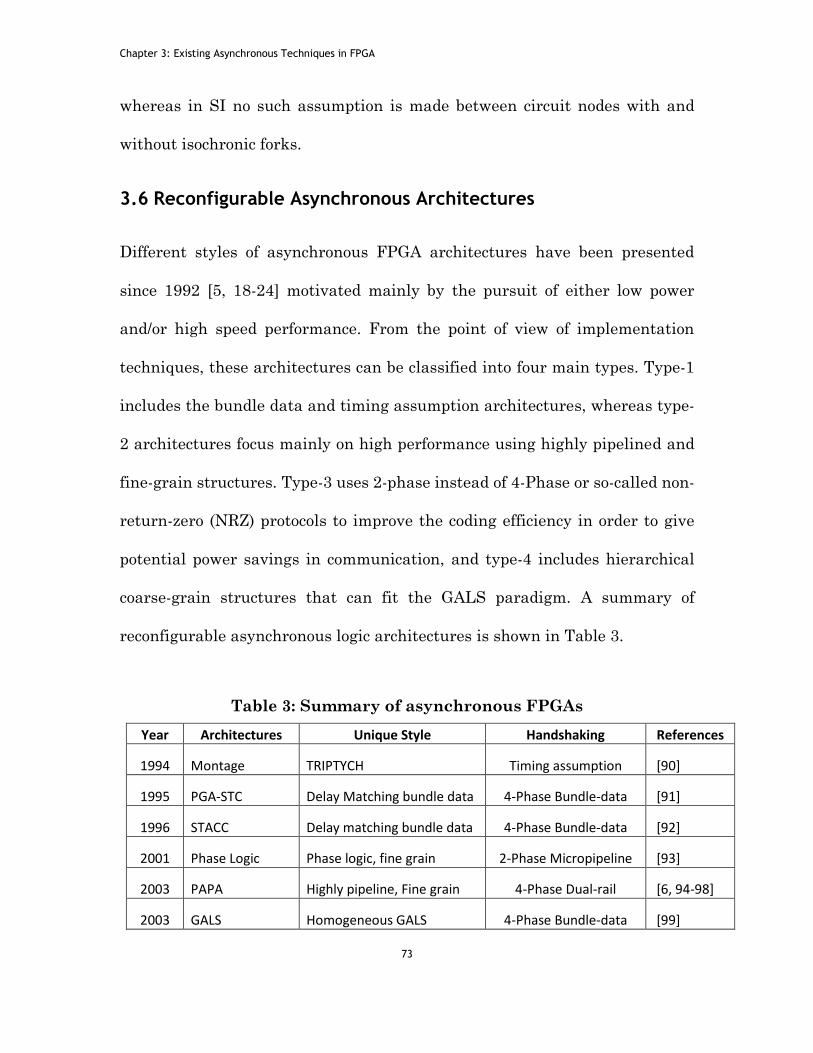
Chapter 3: Existing Asynchronous Techniques in FPGA
73
whereas in SI no such assumption is made between circuit nodes with and
without isochronic forks.
3.6 Reconfigurable Asynchronous Architectures
Different styles of asynchronous FPGA architectures have been presented
since 1992 [5, 18-24] motivated mainly by the pursuit of either low power
and/or high speed performance. From the point of view of implementation
techniques, these architectures can be classified into four main types. Type-1
includes the bundle data and timing assumption architectures, whereas type-
2 architectures focus mainly on high performance using highly pipelined and
fine-grain structures. Type-3 uses 2-phase instead of 4-Phase or so-called non-
return-zero (NRZ) protocols to improve the coding efficiency in order to give
potential power savings in communication, and type-4 includes hierarchical
coarse-grain structures that can fit the GALS paradigm. A summary of
reconfigurable asynchronous logic architectures is shown in Table 3.
Table 3: Summary of asynchronous FPGAs
Year Architectures Unique Style Handshaking References
1994 Montage TRIPTYCH Timing assumption [90]
1995 PGA-STC Delay Matching bundle data 4-Phase Bundle-data [91]
1996 STACC Delay matching bundle data 4-Phase Bundle-data [92]
2001 Phase Logic Phase logic, fine grain 2-Phase Micropipeline [93]
2003 PAPA Highly pipeline, Fine grain 4-Phase Dual-rail [6, 94-98]
2003 GALS Homogeneous GALS 4-Phase Bundle-data [99]

Chapter 3: Existing Asynchronous Techniques in FPGA
74
2003 CalTech Cluster, e1of2 e1of2 [100]
2005 GAPLA Heterogeneous GALS 2-Phase Bundle-data [101, 102]
2007 NCL NULL Convention Logic NCL /QDI [103]
2007 TARTAN NoC (Hierarchical RF architecture) 4-Phase Bundle-bundle [104, 105]
2007 Achronix Pipeline, Fine grain 4-Phase Dual-rail [106]
2008 e-FPGA 1-of-n QDI (security) 1-of-n QDI [85]
2010 Distributed AFPGA David Cell control
Hybrid 4P-DR and Bundle-data [68]
3.6.1 Type-1: Bundle Data and Timing Assumption Architectures
Asynchronous FPGA solutions have been presented in the literature since 1992
[3-14]. Payne [92] provided a summary of the MONTAGE [90], PGA-STC [91],
and STACC [107] .
MONTAGE from the University of Washington proposed in 1994, was the first
asynchronous FPGA, though it includes a clock signal for implementing
synchronous circuits as well. It was extended from their own synchronous
FPGA architecture by adding special arbitration cells and modifying the
function unit. The MONTAGE architecture relies heavily on the regular
routing structure and fast feedback path to achieve state holding on the
functional unit (LUT), as shown in Figure 30. Under variation, the wire delay
of large and long interconnects cannot be guaranteed, and therefore the chance
of glitches occurring is high.

Chapter 3: Existing Asynchronous Techniques in FPGA
75
Figure 30: MONTAGE functional unit (configured as C-Muller gate).
The PGA-STC was developed at U.C. Davis in 1995. The author basically
proposed that the Xilinx XC4000 series structure should be modified [91] by
replacing the clock with programmable delay elements, as shown in Figure 31.
The idea of the delay-matching bundle-data structure is very similar to clock
design but distributed across the whole fabric by matching the timing of each
individual functional-unit computation time. This bundle data technique could
be highly-efficient in terms of minimizing the area and power overhead. Yet
under variation and at below nominal voltage level, the delay element might
suffer more than the function unit itself. The walk-around strategy could be
used to increase the matching delay line with an extra-long margin for
variability, but this will then defeat the objective of self-time implementation
since a similar result in dealing with variation can be achieved in an
asynchronous architecture by lowering the clock speed or by providing an extra
timing margin or guard-band.

Chapter 3: Existing Asynchronous Techniques in FPGA
76
Figure 31: PGA-STC functional block with programmable delay
element.
The STACC is an architecture developed at the University of Edinburgh by
Payne [92]. It is a dedicated architecture for the implementation of four-phase
bundled-data systems. Its architecture is based on that of fine-grain FPGA
architectures where the global clock is replaced by an array of timing-cells that
generate local register control signals. All of the above asynchronous FPGAs
amend the function units to avoid hazards in signals, and use timing
assumptions to guarantee the correctness of the asynchronous circuits. This
structure has been proposed to replace the clock resources with a structure
similar to a micropipeline [108] together with programmable delay (PD)
elements . This could be a promising strategy to deal with variation. However,
the original paper presented a very conceptual design without a detailed
description of implementation and only simulation data.
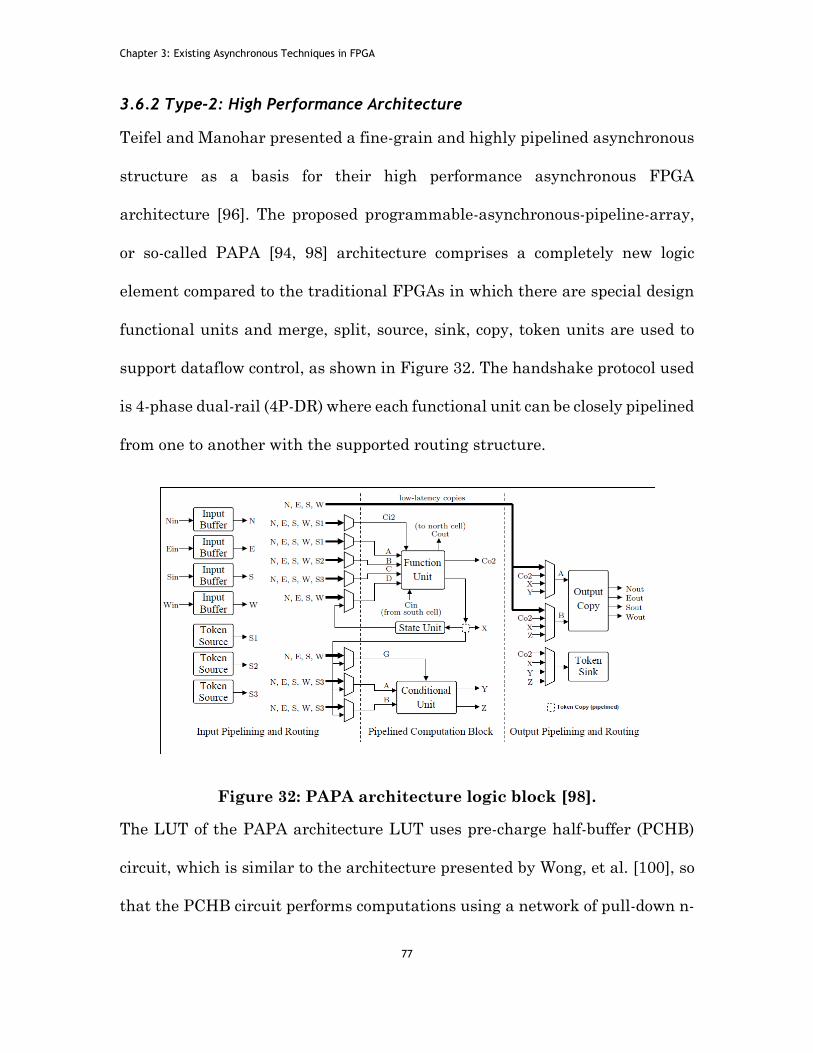
Chapter 3: Existing Asynchronous Techniques in FPGA
77
3.6.2 Type-2: High Performance Architecture
Teifel and Manohar presented a fine-grain and highly pipelined asynchronous
structure as a basis for their high performance asynchronous FPGA
architecture [96]. The proposed programmable-asynchronous-pipeline-array,
or so-called PAPA [94, 98] architecture comprises a completely new logic
element compared to the traditional FPGAs in which there are special design
functional units and merge, split, source, sink, copy, token units are used to
support dataflow control, as shown in Figure 32. The handshake protocol used
is 4-phase dual-rail (4P-DR) where each functional unit can be closely pipelined
from one to another with the supported routing structure.
Figure 32: PAPA architecture logic block [98].
The LUT of the PAPA architecture LUT uses pre-charge half-buffer (PCHB)
circuit, which is similar to the architecture presented by Wong, et al. [100], so
that the PCHB circuit performs computations using a network of pull-down n-

Chapter 3: Existing Asynchronous Techniques in FPGA
78
type transistors. Both architectures use the similar general PCHB template as
the building block, but architecture presented by Wong, et al. [100] is
fundamentally different in that the granularity is coarser with a cluster or
CLB-equivalent structure. Both of these architectures are not only great for
high throughput performance thanks to their inherent pipeline structure, but
also robust to PVT variation as in a QDI circuit. Measurement results [6]
demonstrated that these asynchronous architectures can work at wide ranges
of voltage and temperature. This further proved that this class of asynchronous
circuit designs might be a promising avenue addressing the concerns about
variability.
Several patents have also been successfully filed resulting from collaborative
work on PAPA’s architecture as follows:
Reconfigurable logic fabrics for integrated circuits and systems and
methods for configuring reconfigurable logic fabrics, US 8575959 B2
[109].
Programmable crossbar structures in asynchronous systems, US
8300635 B2 [110].
Synchronous to asynchronous logic conversion, US 8291358 B2 [111].
Programmable asynchronous pipeline arrays, US 7157934 B2 [98].
Chapter 3: Existing Asynchronous Techniques in FPGA
79
The Achronix Semiconductor Corporation [106] used the PAPA
architecture as the basis for the launch of the first commercially available
asynchronous FPGA. Their product family targeted high performance markets
such as the military, networking and telecommunications sectors. Fabricated
at TSMC 65nm technology with a density of 164K LUTs with all the additional
memory, multipliers, SerDes, PLLs and memory controller hard blocks, the
company’s products were claimed to be the fastest FPGAs in the market in
2008 with a maximum frequency of 1.5GHZ [112].
3.6.3 Type-3: Communication Efficiency (2-Phase Dual-Rail or LEDR)
Phase logic (PL) [93] and level-encoded dual-rail (LEDR) [113] both use 2-
phase dual-rail (2P-DR) delay insensitive (DI) data encoding schemes. In this
communication scheme, two wires/rails are used. Similar to the 4-phase dual-
rail (4P-DR), both data and control information are encoded in the dual-rail
package. In 4P-DR, the (0,0) codeword is used as a spacer and (1,1) is unused
or invalid, as shown in Figure 33 (a). In this type of communication, the
codeword always has to return to (0,0) as the “spacer” between valid data.
Whereas, in 2-phase communication the efficient is higher, this is because all
the codewords are set to indicate a valid data. As such, the upper wire/rail of
the code holds the standard single rail data value and the lower one is the
parity bit indicating the phase; see Figure 33(b). Since no return-to-zero phase
is required, the 2-phase or LEDR is also classified as a non-return-to-zero (NRZ)
protocol.

Chapter 3: Existing Asynchronous Techniques in FPGA
80
Figure 33: 4P-DR and LEDR communication.
The uniqueness of this encoding technique lies in the fact that the phase
always alternates with every new data arrived, between phase 0 and phase 1
(or “even” and “odd” phases). For example, in the even phase the code word for
0 = (0,0) and for 1 = (1,1). In the odd phase 0 = (0,1) and 1 = (1,0).
Investigation of the programmable phase logic (PL) with this protocol started
in 2001 by Traver et al. [114-116]. The authors proposed the design of the
LUT4-based phase logic cell to form their basic FPGA logic elements (LEs) as
shown in Figure 34. This was achieved by wrapping the phase control logic
around the 4-input lookup table (LUT4). The idea of keeping the original LUT
structure intact has the potential benefit of minimising the need to completely
redesign or reuse the existing FPGA design tool flow. This bears some
similarity to the work presented in chapter 4, but at a different level of
granularity. The problem with the fine-grain PL structure is that it massively
increases the area overhead with the consequence of higher power leakage
compared to its synchronous counterpart because of the complex coding.
Furthermore, similar to the earlier asynchronous FPGA structures presented
above, the interconnection and communication block that occupied the lion’s

Chapter 3: Existing Asynchronous Techniques in FPGA
81
share of the soft fabric has not been realised and therefore it is difficult to
evaluate their potential power and throughput performance.
Figure 34: LUT4-based phased logic gate [115].
In summary, theoretically, due to the NRZ scheme, the LEDR protocol has
potential advantages compared to the 4-Phase return-to-zero (RZ) protocol in
terms of power and throughput. The potential power improvement is based on
the efficiency of the coding that reduces the number of transitions on the global
interconnect. Also, because the NRZ protocol means that no ‘spacer’ is required,
hence a higher throughput yield may be expected. However, in the hardware
implementation and due to the complex phase detection logic, data encoding
and decoding required, the circuit’s size and power increases significantly
compared to synchronous circuits, for example in the LEDR protocol converter
shown in Figure 35. This overhead makes it impractical to be implemented,
especially at the fine-grain level.

Chapter 3: Existing Asynchronous Techniques in FPGA
82
Figure 35: More complex LEDR protocol converter [117].
Nevertheless, as the subsequent work demonstrated [117-120], the LEDR
protocol can still be beneficial when exploited appropriately. The results
suggest that the strategy should be to employ the LEDR protocol for global
data transfer, leaving the local functional and computational units with the RZ
protocol. Examples of this kind of coarser grain structures are the GALS,
MPSoC and NoC.
3.6.4 Type-4: Hierarchical and Coarse Grain Reconfigurable Architecture
The previous sections have demonstrated that the fine granularity
asynchronous FPGA may have high flexibility and throughput performance,
yet it comes with a silicon size penalty. The robust QDI circuit normally
requires dual-rail interconnects and this may massively increase interconnect
and routing resources composed of switches and configuration bits that
constitute a large proportion of the PPGA soft fabric. The idea of increasing

Chapter 3: Existing Asynchronous Techniques in FPGA
83
granularity by packing together several LUTs to reduce global interconnects is
not new, and may be called the CLB or cluster. However, for certain
applications, increasing the granularity to a higher level such as by grouping
multiple CLBs or functional-units (FUs) together into the same timing domain
may result in better area and power performance. Each group of FUs can work
at their individual local clock domain and the interface between island FUs
will use the asynchronous principle. With the combined benefits of both
synchronous and asynchronous elements, this has given rise to new approach
as such as globally asynchronous and locally synchronous (GALS) and
network-on-chip (NoC) designs.
Figure 36: GALS in FPGA: (a) Homogeneous; (b) Heterogeneous.
Homogeneous GALS
The GALS scheme was introduced in ASICs level as early as 1984 [121], and
Royal and Cheung [99] then proposed to apply the technique to FPGAs. The

Chapter 3: Existing Asynchronous Techniques in FPGA
84
proposed structure uses a 4-phase bundle-data handshake protocol to ease the
synchronization problem for systems with multiple modules working at
different clock domains. The architecture also features micropipelines in the
routing. The unique aspect of the implementation of this architecture
concerned their proposal to convert the conventional synchronous FPGA into
GALS by introducing an asynchronous interface around the regular packed
synchronous block, known as the asynchronous wrapper. This GALS paradigm
introducing an asynchronous circuit at a coarse regular size synchronous block
could reduce the overhead that otherwise may be incur by the fine grain
AFPGA; however the tradeoff would be reduced flexibility. Also, because of the
shapes and sizes of the wrappers for computation blocks across the whole fabric
are the same, as shown in Figure 36 (a), this may reduce the logic utilization
within each island. The authors also recommended using accurately tunable
delay lines, which would have the potential benefit of reducing the effect of
PVT variation [122]. However, this proposed idea required further
development from it conceptual state.
Heterogeneous GALS
Jia and Vemuri [101] proposed a globally asynchronous-locally synchronous
programmable logic array (GALSPLA) architecture together with a CAD tools
design flow [102]. Compared to in [99], their proposed architecture is distinct
in two respects. Firstly, the size and shape of their synchronous logic blocks
are not fixed or can be in heterogeneous shape, which therefore may help in

Chapter 3: Existing Asynchronous Techniques in FPGA
85
improving the logic utilization. Secondly, their asynchronous wrapper uses a
2-phase instead of 4-phase bundle-data communication. Similar to the LEDR,
the tradeoff of this handshaking protocol is better energy and throughput
performance, but the phase conversion circuit may be more complex. The
estimated size overhead for GAPLA architecture adaptation is small (at about
7%), and experimental results showed a performance improvement of 55% can
be expected.
The results show that the concept of using heterogeneous GALS could be
promising. However, from the point of view of variation tolerance, this
proposed architecture may have some limitations due to the fact that bundle-
data handshaking protocols rely heavily on timing assumptions. Furthermore,
at a technology scale beyond 90nm, extrinsic and intrinsic variations become
more prominent. Research has shown that circuits demonstrating the
characteristics of both correlated as well as stochastic variability can be
observed already in commercial off-the-shelf FPGAs [3]. This means that
within the large locally synchronous block, the variability issue still remains.
Networks-on-Chip (NoC)
Networks-on-chip (NoC) represent the next higher level of coarse-grain
architecture that fit well into the GALS paradigm. Instead of the traditional
direct wire-to-wire bus connection, the NoC uses a networking strategy where
data are grouped and transferred in packets. Similar to the pack switching

Chapter 3: Existing Asynchronous Techniques in FPGA
86
network system, routers are needed at each node to communicate data across
the chip. Several asynchronous NoC have been proposed in the literatures that
are composed of asynchronous routers. These include the ASPIN [123]
architecture that uses bundle-data within the router and QDI circuits for long
interlinks, MANGO and QNOC[124] which use standard 4-phase bundle-data
and later use 2-phase mousetrap protocols [125], and the TARTAN [104, 105]
architecture that uses a 4-phase pipelined protocol interfaced with complex
memory support.
3.6.5 Other Asynchronous Style FPGAs
NCL Logic FPGA:
The NULL Convention Logic™ (NCL) [103] was patented and trademarked by
Theseus Logic, Inc. [126] in 1994. It was derived from a mathematical
expression of process completeness and provided inherently convenient in
expressing asynchronous digital circuits.
The NCL is built in a design of 27 fundamental gates with a hysteresis state-
holding capability to retain the output state until all of the input has been de-
asserted again. Each NCL gate is custom-designed at transistor level to exhibit
state holding behaviours similar to those of the C-element.
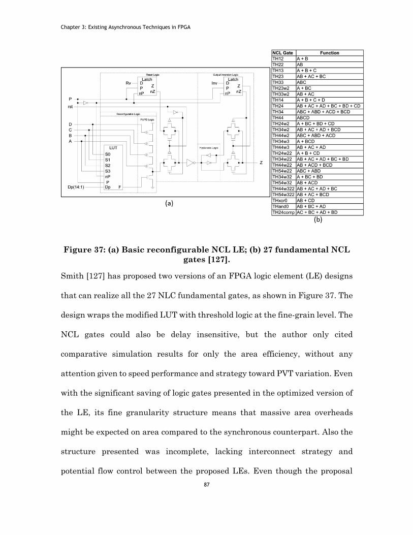
Chapter 3: Existing Asynchronous Techniques in FPGA
87
Figure 37: (a) Basic reconfigurable NCL LE; (b) 27 fundamental NCL
gates [127].
Smith [127] has proposed two versions of an FPGA logic element (LE) designs
that can realize all the 27 NLC fundamental gates, as shown in Figure 37. The
design wraps the modified LUT with threshold logic at the fine-grain level. The
NCL gates could also be delay insensitive, but the author only cited
comparative simulation results for only the area efficiency, without any
attention given to speed performance and strategy toward PVT variation. Even
with the significant saving of logic gates presented in the optimized version of
the LE, its fine granularity structure means that massive area overheads
might be expected on area compared to the synchronous counterpart. Also the
structure presented was incomplete, lacking interconnect strategy and
potential flow control between the proposed LEs. Even though the proposal

Chapter 3: Existing Asynchronous Techniques in FPGA
88
was later elaborated [128] with grouped LEs or CLB for hierarchical approach,
the work is still very immature in terms of what be required to form a basic
FPGA architecture.
Multi-Style and SAFE – eFPGA
The TIMA Lab in France has presented a unique fully-customized
asynchronous FPGA that has been prototyped in 65nm CMOS technology [85,
129, 130]. The architecture supports multiple style asynchronous logic,
including 2-phase, 4-phase communication protocols and 1-of-n encoding. The
main motivation for using asynchronous logic in this work was to present an
electrically balanced circuit that is robust against side channel attacks (SCAs)
dedicated for security applications.
The lack of a global clock in asynchronous logic mean that the system is more
immune to simple-power-attack (SPA) and differential-power-analysis (DPA)
attacks, and the QDI circuits or the general 1-of-n coding lead to data
computation and communication at a stable Hamming weight. This reduces
the power consumption dependency that can be exploited by SPA, DPA and
electromagnetic-analysis (EMA) attacks.
The research in the above work focuses on two aspects. The first is a platform
to support flexible styles of asynchronous implementation, and the second is to
increase security levels against SCAs. The inherently asynchronous structure
may also be robust to environmental variation, yet no relevant data was

Chapter 3: Existing Asynchronous Techniques in FPGA
89
presented by the authors. The security benefits of asynchronous logic might be
an interesting direction for investigation in research but is not the main focus
of the present study. It should also be noted that flexibility in style also implies
that extra configurability resources are needed and will this consequently
increase silicon area and power overheads.
3.7 Summary
This chapter has presented an overview of commonly used asynchronous
design styles including the bundle-data and dual-rail communication schemes.
The asynchronous techniques applied on FPGA in the past decade have been
reviewed. Motivated by either lower power, high throughput performance and
in the context of variation tolerance, these architectures summarised as follows:
Type-1, the early development of the AFPGA relied on significant elements of
timing assumptions to guarantee the correctness of the asynchronous logic.
This method combines the delays for both FPGA intra-block and inter-block
connections and replaces the local timing assumption with global timing
assumption. In general, these types of asynchronous circuits are easier to
implement and may be with less overhead. However, it is hard to match delays
for FPGA inter-block connections since the connection path cannot be
determined at design time. In the larger technology node wire delay can be
negligible compare to the logic delay, but at modern sub-nano meter technology,
Chapter 3: Existing Asynchronous Techniques in FPGA
90
delay matching based on delay assumption is hard to achieve especially
considering process and environmental variations.
Type-2, this advanced development of the AFPGA focuses on high performance.
On the one hand, they are somewhat tolerant to operational variations (process,
voltage, temperature) through SI/DI with none or minimal reliance on timing
assumptions. On the other hand, they modify the entire FPGA fabric and
replace the fundamental basic logic block of current FPGA technology. This
makes the system design process less accessible by significantly reducing the
usefulness of existing design tools. Furthermore, some of these architectures
utilised very fine-grained pipelined architectures consisting of excessive
numbers of C-elements, implying high area and power overheads.
Type-3, 2-Phase Dual-rail (2P-DR) and LEDR architecture aim to improve
power and throughput with the optimised NRZ scheme rather the 4-Phase
return-to-zero communication. Theoretically, higher throughput and less
energy would be expected because of reduced transitions on the global
interconnect. However, due to complex hardware implementation of the phase
detection circuit, the benefit maybe offset with the increase of circuit size. This
overhead will increase significantly if implemented at fine-grain levels.
Type-4: As for the NoC and GALS, the trade-off arguments are the same, where
the higher or coarser grain architecture will improve power efficiency but the
challenges in technology scaling and increase in logic density result in
Chapter 3: Existing Asynchronous Techniques in FPGA
91
inevitable variability issues that affect the chip at both the global and local
levels.
With the technology scaling continues and transistor sizes shrink to the
nanoscale, timing variability have becomes a growing concern. Maintaining
global clock in multimillion logic cells FPGA is becoming difficult; therefore
asynchronous design styles are receiving growing attention, since
asynchronous circuits operation do not rely on tight timing margins. Although
various style asynchronous FPGAs exist as presented in this chapter, but they
have not achieved it widespread use compare to its synchronous counterpart
due two main reasons. Firstly, its lack of supportive automated design tool and
unfamiliarity of the non-clock design concept to the community. Most of
asynchronous architectures presented in the study modified the traditional
structure greatly and make it hard to incorporate or to reuse with existing
design flows. Secondly, asynchronous handshaking logic normally incurs large
area overhead especially implemented in fine granularity level.
The works in this research focus on improving the reliability of the FPGA
architecture with the support of asynchronous techniques while keeping most
the fundamental structure of traditional FPGA intact and therefore allows the
reuse of existing commercial design flows. The proposed architecture will
compromise between types (1), (2) and (4). The objective is tries to strike a
sensible balance between maintaining the fundamental FPGA’s structures
whilst achieving full asynchrony in places where it matters most as follow:

Chapter 3: Existing Asynchronous Techniques in FPGA
92
1. Maintaining the existing FPGA block structure and maintain the
possible reuse of existing commercial design flow.
2. Making critical interconnects paths DI for latency variation tolerance.
3. Improve or at least maintain throughput performance.
4. Keep the area and power overhead of the asynchronous handshaking
logic at minimum by clustering the logic block similar to type-4 but
balance at the right granularity level.
Chapter 4 present the implementation and analysis of the asynchronous FPGA
architecture base on the above specification.

Chapter 4: Distributed Control Asynchronous FPGA Architecture
93
Chapter 4. Distributed Control Asynchronous FPGA Architecture
4.1 Introduction
As mention in the previous chapter, the purpose of this work is to investigate
a practical approach from the architecture point of view to deal with the
variability challenges faced in the current and future FPGA technology.
Asynchronous logic is known to be highly resilient to variability; therefore the
potential for this approach is attractive. However, various trades-offs with
asynchronous logic implementation need to be studied in detail in the context
of field programmable gate arrays (FPGA). This chapter proposes an
asynchronous FPGA architecture that maintains the basic logic element of the
conventional FPGAs, allowing maximum reusability of existing automatic
design flows. Interconnects of this architecture are delay-insensitive (DI) and
the handshaking is achieved through a distributed controller on every cluster.
This architecture is mainly aimed to tolerate latency variability resulting from
the process and environmental variations in modern CMOS process technology.
In addition, this newly proposed asynchronous architecture also facilitates the
investigation of systems powered by nondeterministic Vdd sources such as
energy harvesting systems. Variation tolerance of the architecture is achieved
by retaining the local computational logic element in single-rail and replacing
the global clock resources with DI handshaking interconnects. The remainder

Chapter 4: Distributed Control Asynchronous FPGA Architecture
94
of the chapter describes the implementation of the medium-grain wrapper
based asynchronous FPGA structure and its essential components in detail
followed by a proposed design flow. Variability simulation results are also
presented with case study implementations.
4.2 Asynchronous Wrapper
The Fully-Asynchronous FPGA architectures that are fine-grain or completely
modified the conventional FPGA structure, for example the highly-pipelined
PAPA architecture [94, 96] may be highly resistant to variation. However,
these architectures come with high area and power overheads. Moreover, the
design process for fine-grain FPGAs is not straightforward and usually
presents a steep learning curve to the designer.
The proposition of wrapping the synchronous-block or Intellectual-property (IP)
units with handshaking logic that communicated asynchronously is not new.
Such GALS scheme has been introduced since early 80’s [121] and was later
proposed to apply the technique to FPGAs in [99]. However GALS scheme is
normally coarse-grain architecture. The granularity of the GALS scheme
affects the logic usability and tolerability and not able tolerate random
variation within the synchronous island block. Also, such systems generally
require a significant alteration of existing FPGA tool design flow. Therefore
one strategy to increase acceptability is to retain the existing design flow as
much as possible. This can be done by keeping the underlying FPGA’s logic

Chapter 4: Distributed Control Asynchronous FPGA Architecture
95
structure untouched and introducing a wrapper circuit around it to replace the
clock tree. This would allow the reuse of the flow in logic synthesis, with the
optimisation and packing processes largely the same for the data path.
In addition, asynchronous circuits tend to be based on relatively complex
coding methods, such as 4-phase dual-rail (4P-DR) or, in general, m-of-n [83].
This implies large area overheads. Asynchronous circuits supposedly involve
low power since they can be made to work only when necessary and do not
require clock trees. However, in general, complex coding may result in an
increase of interconnects and switching activities in the FPGAs unless in low
power coding such as 1-of-4, leading to more dynamic power consumption,
potentially negating the savings from removing clock signals. The larger circuit
size may also lead to greater power leakage. Thus the proposed wrapper
structure is medium-grain, with one wrapper per cluster. This structure sits
between the fine-grain structure, with one wrapper per logic cell, which is high
in area overhead and dynamic power, and the fixed coarse-grain structure with
one wrapper per multiple clusters may reduce the number of global
interconnects but potentially also reduces its logic utilisation such as in the
GALS or NoC approaches. The top-down descriptions of the distributed control
asynchronous wrapper in the FPGA architecture are given as follows.
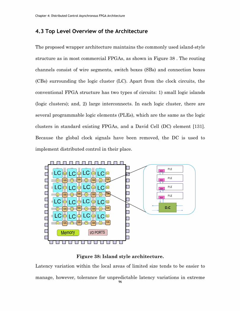
Chapter 4: Distributed Control Asynchronous FPGA Architecture
96
4.3 Top Level Overview of the Architecture
The proposed wrapper architecture maintains the commonly used island-style
structure as in most commercial FPGAs, as shown in Figure 38 . The routing
channels consist of wire segments, switch boxes (SBs) and connection boxes
(CBs) surrounding the logic cluster (LC). Apart from the clock circuits, the
conventional FPGA structure has two types of circuits: 1) small logic islands
(logic clusters); and, 2) large interconnects. In each logic cluster, there are
several programmable logic elements (PLEs), which are the same as the logic
clusters in standard existing FPGAs, and a David Cell (DC) element [131].
Because the global clock signals have been removed, the DC is used to
implement distributed control in their place.
Figure 38: Island style architecture.
Latency variation within the local areas of limited size tends to be easier to
manage, however, tolerance for unpredictable latency variations in extreme

Chapter 4: Distributed Control Asynchronous FPGA Architecture
97
cases is more crucial for long interconnects. Therefore the approach taken is
retaining the basic conventional FPGA cluster-based structure relatively
unchanged, this makes each of the cluster behave functionally as a block self-
timed to its environment and replace the synchronous clocking resources with
distributed DC-based control and DI interconnects. The design of the LC and
the principles of DC control are demonstrated in the following sections.
Table 4: Choice of architecture structure.
Architecture Overview
Parameter value Reference
Architecture Island style [132]
LUT Size (K) 4 * Inputs [133]
Logic Cluster Size (N) 4 * PLE [133]
Cluster input Channels (i) 16 [133]
Channel Type Dual- rail/Channel [83]
Switch Box (SB) Universal [134]
Connection Box (CB) Normal [134]
Process Technology UMC-90nm CMOS -
Handshake Protocol 4-Phase Dual-Rail [83]
David Cell (DC) [135]
The granularity or structure choice of FPGA affects the logic utilization, speed
and power performance. This is usually based on three vital logic cluster

Chapter 4: Distributed Control Asynchronous FPGA Architecture
98
parameters which are the size (K) of the lookup table (LUT), the cluster size
(N) or the number of LUTs in a cluster, and the number of inputs per cluster
(I). In general, increasing the sizes of K and N will improve functionality and
performance, but at the same time escalate the area exponentially. Cluster
input size, I, should be kept as small as possible; however, if I is too small,
numerous logic elements in the cluster may be unavailing [9, 136]. The classic
FPGA architecture uses four LUTs per cluster and four inputs for each LUT.
In this setup, the default values are chosen. Table 4 shows the structural
choices made for the proposed asynchronous FPGA architecture.
4.4 Asynchronous Wrapper Structure
The fundamental block of a conventional FPGA comprises a lookup table (LUT),
a register (DFF) and a multiplexer (MUX). The terminology in Altera is called
a logic element (LE) or logic cell in Xilinx. In this design, asynchronous logics
are introduced wrapping around the fundamental logic blocks or LEs. The
newly designed structure that combines the wrapper and logic blocks
constitutes the new programmable logic element (PLE). This is shown in
Figure 39.

Chapter 4: Distributed Control Asynchronous FPGA Architecture
99
Figure 39: Wrapper based programmable logic element (PLE).
The wrapper consists of the following circuits:
Programmable completion detection (PCD)
Trigger selection switch (SW)
Programmable delay (PD)
Single- to dual-rail converter (CONV)
Completion detection (CD)
The PCD is used to compute the complete arrival of all valid data. When all
data arrived, two “ready” signals will be generated from the PCD. This is for
the two possible used for this input data. Firstly, if the data could be used for
an operation involving only the local PLE the “ready” signal goes directly to
the (T.SW – “to SW”) to enable the local LUT to start data processing. Secondly,
the data may be used for a concurrent operation with other PLEs which may
or may not be in the same cluster. In this case, the ready signal goes to the
David Cell (DC)-based distributed control to synchronize with the input data
for other PLEs (via T.DC – “to DC”) and when the synchronization is complete,
the SW will be enabled by the F.DC (“from DC”) signal from the DC circuit.
Chapter 4: Distributed Control Asynchronous FPGA Architecture
100
The SW is basically a dual-input multiplexer which can select ready signal
either directly from the PCD or from the distributed DC control when
synchronization is required. In order to minimize the intermediate transitional
activities of the circuit and guarantee that the LUT is activated only when the
data is ready for the entire operation, the enable logic is implemented on the
LUT.
The PD is used to set up delays to match with certain operations. Here the first
PD is used to match the latency of the LUT and the second PD the latency of
the latch data and to indicate the “ready” state of the single-rail data from the
MUX.
CONV is purposed to transform the original single-rail data into a dual-rail
encoded data for DI communication. CD is completion detection indicating
validity of dual-rail data has been generated. The CD is optional depending on
where the control signal came from (either “T.SW” for independent
acknowledgement or “F.DC” for consolidate acknowledgement).
The wrapper commission in the following manner, when all input valid data
are detected, PCD generates a trigger signal. The trigger signal will then act
as a start indication for LUT to commence computation. PDs match the
computation time and used to control the effective latching timing. The
computed result can be then converted from single-rail data to dual-rail before
propagating to the next stage. The output of the CD is an “ACK” or “Done”

Chapter 4: Distributed Control Asynchronous FPGA Architecture
101
signal, generated to the previous stages when the input data has been
consumed.
4.4.1 Programmable Completion Detection (PCD)
Figure 40: Programmable completion detection.
The PCD is the programmable completion detection circuit constituted with C-
element and OR-gates as shown in Figure 40. The OR-gates allows the
straightforward detection of valid signals from spacers or empty code-words in
dual-rail encoding. The typical dual-rail code show in Table 5
Table 5: Dual-rail code-words.
Code-words Code
0,0 Spacer
0,1 0
1,0 1
1,1 Not valid
Because the code-word (1, 1) is illegal and cannot occur, an OR gate is sufficient
to safely indicate that a single data channel is “valid” or “empty”.
The completion detection valid-signals can be achieved with C-element that is
a commonly used component in asynchronous circuits [83]. The C-element
Chapter 4: Distributed Control Asynchronous FPGA Architecture
102
provides the hysteresis in the empty-to-valid and valid-to-empty transitions
required for transparent handshaking. It waits till all inputs to be valid before
setting the output to high, and waits for all its inputs to become empty to set
the output to low. For other input combinations, the output does not change.
C-elements are thus ideal for collecting the states of multiple channels.
The proposed PLE, the input size of the C-element is four, however, in the
actual implementation, not all input will be usable. In order to allow the 4-
inputs C-element to function correctly, flexibility configuration are required in
such case. This is resolved by utilising extra three multiplexers to link the idle
channel (B, C or D) to Channel A, which is assumed to be always in operative
if the PLE participates in the computation. The process of enabling or disabling
the relevant MUX for the relative channel is assumed to be handled by
automated tools during the synthesis and mapping flow.
4.4.2 Switch Box (SW) Circuit
The SW trigger switch box in Figure 41 is a simple programmable multiplexer.
The purpose of this SW is to facilitate the selection of the trigger or valid signal
between the PCD block and the DC-control. For concurrent operation, the
“F.DC” signal is used to synchronise operation for multiple PLEs. The example,
the subsequent case study section clarifies the function of the SW.

Chapter 4: Distributed Control Asynchronous FPGA Architecture
103
Figure 41: SW box circuit.
4.4.3 Programmable Delay (PD) Unit
The bundle-data is one of the most efficient approach asynchronous
handshaking. Delay-element is used here for matching for the latency of the
data path element being bundled; this local control signal has the equivalent
functions of clocks of conventional LE. Various delay elements was introduces
in chapter 3. However, the most common implementation is the chain-
inverters circuit. Considering the process and environmental variation, the
presented PD is made to be tuneable. The circuit with four selectable ranges
PD is shown in Figure 42.
Figure 42: Programmable delay circuit.
Provided that the variability information concerning the environmental and
power supply is availble from characterisation process, the PD range can be

Chapter 4: Distributed Control Asynchronous FPGA Architecture
104
set at configure time. The PD also can be beneficial in facilitating variation
mitigation techniques such as chip-wise configuration or late binding [3].
In order to retain average rather the worst-case performance under a wide
range of variability, finer tune of programmable delay element may be required.
However, the implication is higher area overheads in PDs.
4.4.4 Single-Rail to Dual-Rail Conversion Circuit (CONV)
Converting the single-rail data output from LE to dual-rail format for the DI
interconnects is the responsibility of CONV in Figure 39. This is shown in
Figure 43.
Figure 43: Dual-rail conversion or DEMUX circuit
At the input of the LE, one of the data wires gives the single-rail binary value
of valid code-words directly. Once it has been ensured that spacers do not
propagate to LE, this wire can be used directly for the data input.
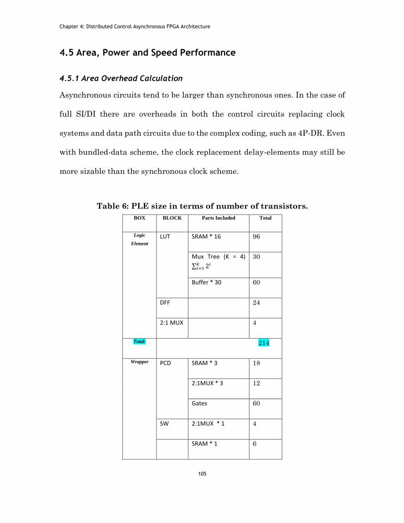
Chapter 4: Distributed Control Asynchronous FPGA Architecture
105
4.5 Area, Power and Speed Performance
4.5.1 Area Overhead Calculation
Asynchronous circuits tend to be larger than synchronous ones. In the case of
full SI/DI there are overheads in both the control circuits replacing clock
systems and data path circuits due to the complex coding, such as 4P-DR. Even
with bundled-data scheme, the clock replacement delay-elements may still be
more sizable than the synchronous clock scheme.
Table 6: PLE size in terms of number of transistors.
BOX BLOCK Parts Included Total
Logic
Element
LUT SRAM * 16 96
Mux Tree (K = 4)
∑ 2𝑖𝑘𝑖=1
30
Buffer * 30 60
DFF 24
2:1 MUX 4
Total: 214
Wrapper PCD SRAM * 3 18
2:1MUX * 3 12
Gates 60
SW 2:1MUX * 1 4
SRAM * 1 6

Chapter 4: Distributed Control Asynchronous FPGA Architecture
106
(PD)*2 (Buffer * 10) * 2 40
(4:1MUX ) * 2 20
(SRAM * 2)*2 24
CONV 2:1MUX * 2 8
Buffer 2
CD OR2 6
Total: 200
With this added resource, many advantages can be gained. This includes
improved variation resilience, avoiding the inevitable issues synchronous clock
systems face with technology scaling, and lower power utilisation in low duty-
cycle process.
Table 6 shows the complexity of the proposed PLE. Notably, the wrapper
circuit introduced consist of almost equal number of circuit elements to the LE
itself. This implies that the PLE is almost twice as big in terms of size. Despite,
the circuit size overhead, the following power analysis shows that power does
not increase much.
4.5.2 Power Comparison
The proposed PLE is roughly double in size the conventional LE. Typically,
bigger the circuit higher the dynamic power consumption, but this PLE uses
asynchronous techniques, which is even driven and without the complex global

Chapter 4: Distributed Control Asynchronous FPGA Architecture
107
clock tree should save the power used. Yet, the combined effect of these changes
is uncertain. Although power optimisation is not the main focus for this section,
it needs to be studied to see if there any radical changes are likely.
The most fundamental block or the PLE is used as an example. As variations
are introduced, it is unreasonable to predict that all of the data will arrive at
the same time. Here the worst case has been assumed where all four data bits
arrive at different moments in time. This has no effect on the synchronous
FPGA, since correct operations are guaranteed by the global clock. Only during
the clock rising edge, stable data is required. But this is achieved by spending
power on clocks. In the proposed AFPGA, data computation starts only when
all of the data has arrived.
Figure 44: (a) Synchronous LUT; and (b) PCD asynchronous LUT.
The power consumption of conventional SRAM-based LUTs and CD-based
LUTs are investigated in a comparative study using the following set-up shown
in (Figure 44):
Four signals, namely A, B, C and D, arrive at the input of LUT at different
times.

Chapter 4: Distributed Control Asynchronous FPGA Architecture
108
Signal A is assumed to arrive last and other signals were changing before it
becomes stable, with 16 transitions between “0000” to “1111”, changing 1 bit
at a time.
When every signal, including ‘A’, eventually settles, output ‘1’ will be
produced.
The simulation results are shown in Figure 45. When there is a transition in
an input signal, the power line will spike. In the synchronous circuit, every
change of data between valid clock signals changes the state of the LUT
address and consumes energy. In the asynchronous design, data will not be
read from the SRAM until it has received the enable signal (En) from the PCD,
as shown in Figure 45 (b). The PCD circuit consumes relatively little power,
and they are corresponds to the tiny power spikes between each pair of high
power signature spikes in Figure 45 (a) and (b).

Chapter 4: Distributed Control Asynchronous FPGA Architecture
109
Figure 45: Operation power: (a) synchronous LUT with timing clock;
(b) asynchronous LUT with PCD.
This simulation shows that, although the size of the PLE circuit has increased,
it consumes roughly the same power and energy as the equivalent clock based-
LUT in this setup. Taking into account the power used by the clock tree circuit
and dynamic clock transition, the asynchronous LUT with CD may produce
better power consumption characteristics in overall. The power data can be
found in Table 7. The simulation is relevant to a relatively low duty-cycle
situation, but because clock distribution is not included for the synchronous
case, it was not put at an unfair disadvantage.

Chapter 4: Distributed Control Asynchronous FPGA Architecture
110
Table 7: Power and energy comparison.
Circuit Operation
Energy
Average
Single
Operation
Power
Operating
Voltage
LE
(sync)
1.037pJ 32.41uW 1.0V
PLE
(async)
0.544pJ 17.00uW 1.0V
Both the power and area comparisons may show significant advantages for the
asynchronous architecture if the clock tree network resources are taken into
account. In the synchronous FPGA, the clock itself brings challenges ranging
from skew, tree distribution and global buffers. Special resources, such as
DLLs (dynamic link libraries), PLLs (phase-locked loops) and clock multipliers,
are also needed. Taking all of this into account, the clock resources in the
synchronous FPGA will require significant amounts of area, power and
management effort. In general, a 10% overhead on the maximum clock rate is
recommended to guarantee operation in the presence of temperature variation.
Due to the scaling of CMOS feature size, FPGA density increases, replacing
the complex global clock with the asynchronous handshaking circuit provides
a promising solution to alleviate the above-mentioned problems [137].

Chapter 4: Distributed Control Asynchronous FPGA Architecture
111
4.5.3 Throughput Performance
In synchronous system design, maximum operating frequency is set based on
the critical path, and normally the maximum clock frequency is set according
to it. In asynchronous system design, there is no global clock. Data is
transferred through stages of logic controlled by handshake protocols which
are inherently pipelined. The faster the data can be transferred from input to
output, the higher the throughput can be achieved. To evaluate the maximum
operating rate, the configuration bits or SRAM of the PLE is first configured
with predetermine logic (within Cadence Virtuoso environment) and the input
signals are stimulated. The time between the complete valid input data having
arrived and valid output generated was recorded. The inverse of the delay from
input to output is the frequency. The peak frequency of the proposed
architecture was compared with those of various reported asynchronous
FPGAs and also a commercial synchronous FPGA (Xilinx-Spartan3). Table 8
shows the throughput performance of various architectures based the
literature at their nominal voltage level. Throughput performance of this work
based on a single proposed PLE also included as a reference.
Table 8: Throughput comparisons of various architectures.
Architecture Technology Peak Throughput Nominal
Voltage
[100] 0.18um 235MHz 1.8V
[94] 0.25um 395MHz 2.5V

Chapter 4: Distributed Control Asynchronous FPGA Architecture
112
[6] 0.18um 674MHZ 1.8V
AFPGA (this work) 90nm 1.5GHz 1.0V
[138] 90nm 326MHz system
clock
1.2V
Variations may result in changes in signal arriving times. A signal arriving too
early or too late may lead to hold and set-up violations in synchronous system
design. This can be dealt with by slowing down the clock by an appropriate
degree to allow extra margins for safety reasons. However the problem of
deriving the appropriate degree of slow-down in any case is significantly non-
trivial [75]. In general, a 10% slowing down on the maximum clock rate has
been recommended for temperature variation [137]. However, the results of
another study [139] indicate that chip frequency variation can be up to 30%.
Table 8 shows that, at a constant Vdd, all asynchronous FPGAs are faster than
the synchronous Xilinx Spartan3. Moreover, the experiment described in the
next section demonstrates that the asynchronous structure also exhibits the
elastic operation of the PLE at a continuously changing Vdd without the
necessity for specific retiming and slowing down.
4.6 Variability Evaluation
4.6.1 PLE Characterisation with Variable Vdd
The simulation of the PLE circuit was on Cadance tools on UMC 90nm CMOS
technology. In the analog design flows, the PLE circuit works correctly as

Chapter 4: Distributed Control Asynchronous FPGA Architecture
113
designed without logic errors with Vdd sweep between 0.45V~1.00V. The result
for delay and energy-per-operation over Vdd performance is shown in Figure
46.
Figure 46: Delay and operational energy at below nominal Vdd level:
(a) results table; (b) delay and energy plot over Vdd.
During the simulation, the circuit shows error operation when Vdd is dropped
below 0.40V. The observation on the timing graph indicated that this is due to
the mismatch in bundling data in PD. Similar phenomenon, has previously
been noticed [140], where inverter-chains based delay-element not maintain
the correct temporal bundling for memory circuits (such as the SRAM cells
here in the LUT) when Vdd is lowered towards the sub-threshold region. This
is due to the rates of slowing down on data path are not in parallel with the
delay-element when Vdd is reduced.
The PLE works well under different but constant Vdds as long as the bundling
delay are matched. In terms of energy usage performance, the result is as

Chapter 4: Distributed Control Asynchronous FPGA Architecture
114
expected where operation energy are reduced with the drop of Vdd. Another
observation from the graph indicated that there is a significant increase in
latency when lowering the Vdd below 0.6V where the two lines crossed as in
Figure 46 (b), this is the optimum operation energy point where significant
energy savings can be achieved without much scarified on speed performance.
Simulation result in Figure 47 shows that the circuit work correctly within
0.45-1.0V constant Vdd range. Further simulation is carried out to investigate
how the PLE behaves under a continuous varying Vdd over the range Vdd rage.
In this experiment, a relatively slow sinusoid signal was applied to the power
supply instead. The LE was configured as a parity checker for the value of A,
B, and C and D. The experiment setup was in self-looping test environment
with the feedback on the completion triggering the next operation. Figure 47
shows that the parity-checker was producing correct “even parity” bits on the
output line continuously under varying Vdd. The output speed (out) and power
rate (Pwr) are relative to the level of the Vdd.
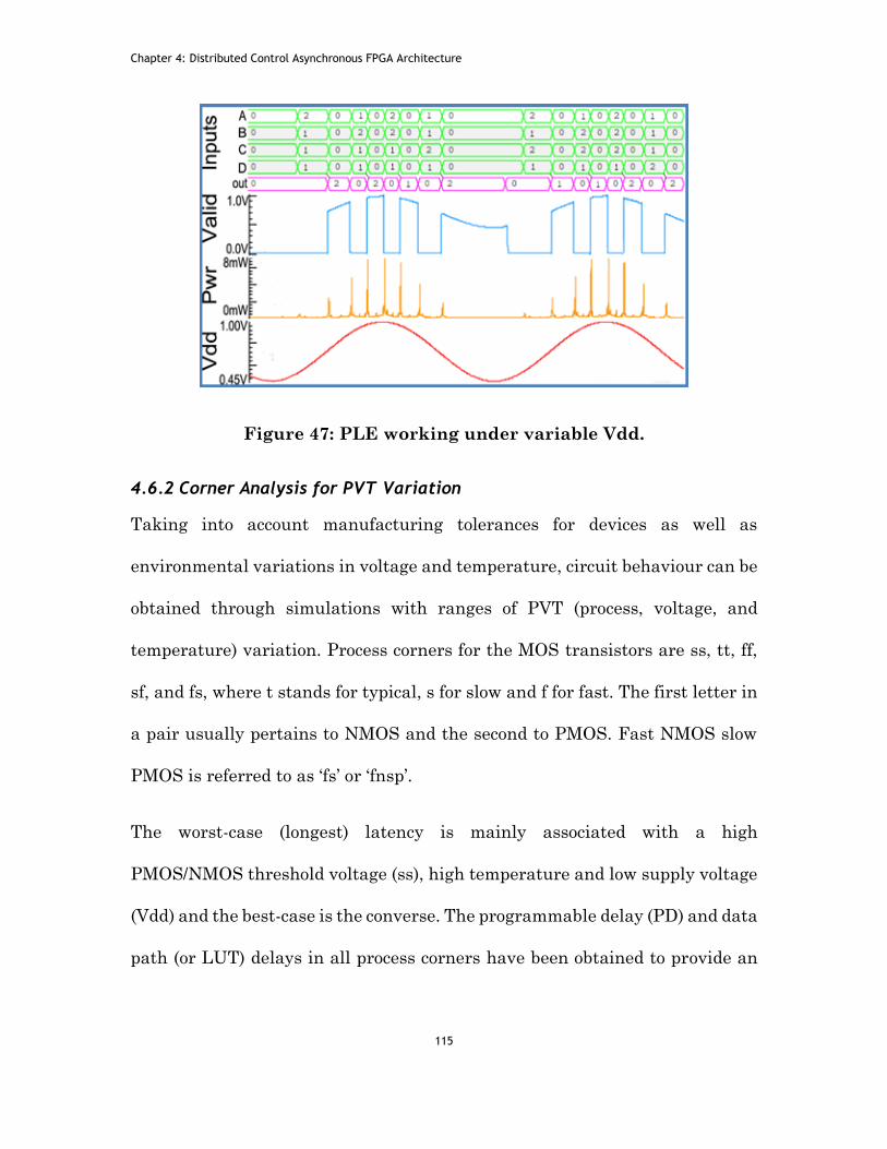
Chapter 4: Distributed Control Asynchronous FPGA Architecture
115
Figure 47: PLE working under variable Vdd.
4.6.2 Corner Analysis for PVT Variation
Taking into account manufacturing tolerances for devices as well as
environmental variations in voltage and temperature, circuit behaviour can be
obtained through simulations with ranges of PVT (process, voltage, and
temperature) variation. Process corners for the MOS transistors are ss, tt, ff,
sf, and fs, where t stands for typical, s for slow and f for fast. The first letter in
a pair usually pertains to NMOS and the second to PMOS. Fast NMOS slow
PMOS is referred to as ‘fs’ or ‘fnsp’.
The worst-case (longest) latency is mainly associated with a high
PMOS/NMOS threshold voltage (ss), high temperature and low supply voltage
(Vdd) and the best-case is the converse. The programmable delay (PD) and data
path (or LUT) delays in all process corners have been obtained to provide an

Chapter 4: Distributed Control Asynchronous FPGA Architecture
116
overview of the best- and worst-case scenarios for the circuit with respect to
slow and fast environments:
Slow environment corners (V =0.5v & T=400K):
LUT (ss: tt: ff: snfp: fnsp) = (1.56ns: 0.79ns: 0.43ns: 0.82ns: 0.75ns)
PD (ss: tt: ff: snfp: fnsp) = (1.82ns: 0.91ns: 0.53ns: 1.01ns: 0.84ns)
Fast environnement corners (V=1.2V & T=273K) :
LUT (ss: tt: ff: snfp: fnsp) = (0.20ns: 0.15ns: 0.12ns: 0.18ns: 0.14ns)
PD (ss: tt: ff: snfp: fnsp) = (0.22ns: 0.16ns: 0.13ns: 0.19ns: 0.15ns)
Figure 48 (a) and (b) show that this PD successfully bundled the LUT delay
across a wide voltage range when both are in the ss & ff corners. Further
analysis was carried out to study cases where the PD and the LUT are in
different corners. The results show that miss matches can occur in both slow
and typical corners as shown in Figure 49(a) and (b). This demonstrates the
need for the use of programmable delays (PD) as mentioned in section 4.4.3
above.

Chapter 4: Distributed Control Asynchronous FPGA Architecture
117
Figure 48: PD and LUT delay successfully bundling: (a) Slow corner
(temperature=400K). (b) Fast corner (temperature=273K).
Figure 49: Cross over at (sf): corner (a) Temperature=300K. (b)
Temperature=273K.
4.7 Logic Cluster Design
The logic cluster (LC), consisting of a group of PLEs, is the next level in the
hierarchy. The unit in the same hierarchical layer in conventional FPGAs is
known as the configurable logic block (CLB) in Xilinx terminology and the logic
array block (LAB) in that of Altera.

Chapter 4: Distributed Control Asynchronous FPGA Architecture
118
Similar to most commercial FPGAs, the cluster in the proposed architecture
(Figure 50) consists of four PLEs with the addition of one David cell (DC),
which forms part of distributed intra-cluster and inter-cluster control. The
general cluster structure is shown in Figure 50.
The DC-based distributed control in the cluster takes charge of the control path.
When input data is ready, the PCDs in the PLEs in the cluster will generate
trigger signals which may be collected by the DC control for group triggering.
Some PLEs may need to execute concurrently and others sequentially. The SW
allows either the selection of self-triggering directly from its corresponding
PCD for sequential operation or group-triggering from the DC for concurrent
operation. After computation is completed, the DC withdraws the data and
propagates the control signal to the next stage. This structure also allows data
feedback channels from the output of each PLE to the input PCDs of other
PLEs. The principle of DC control is demonstrated in an example in the
following section.

Chapter 4: Distributed Control Asynchronous FPGA Architecture
119
Figure 50: Logic cluster with DC.
4.7.1 Distributed Control with David Cell
In this proposed architecture, David Cells (DCs) are used to implement the
distributed control, since this kind of control works based on handshake
protocols. Distributed control using DCs was first proposed by David [131].
Extensions with the direct mapping of asynchronous control circuits from Petri
Nets to DCs have also been reported [135, 141-143].
Basic structures of DCs are shown in Figure 51 (a), consisting of two inputs
(“set” & “reset”), two outputs (“back” & “Fw”), and an SR latch for state keeping

Chapter 4: Distributed Control Asynchronous FPGA Architecture
120
(Q and Qb). Both of the inputs are active-low in the implementation. When the
input “set” is active, Q will be set to high and the inversely active “reset” input
will set Q back to low. The “back” output signal basically works as an
acknowledgement of the previous stage of the pipeline for the signal having
been received, and the “Fw” output signal tells the next stage that the new
signal is ready to be consumed.
Figure 51 (b) shows how the basic structure of DC can be modified as
distributed control for PLEs for computation in the cluster. The signal coming
into a logic cluster can be from multiple sources, and therefore there will be a
group of “set” signals (s1 – sn) to trigger signal “Q”. When the control signal
“Q” is activated, computation will start. An acknowledgement signal “ack” will
then be generated after the valid signal of the valid output has been produce
by the CD circuit. The “ack” signal replaces the “back” signal of the basic DC
structure. Likewise for the output, there may be multiple reset signals (r1 - rn)
to reset the control signal “Q” of the DC.

Chapter 4: Distributed Control Asynchronous FPGA Architecture
121
Figure 51: (a) Basic David cell Structure; (b) DC for distributed
control; (c) set and reset logic boxes for DC implementations.
The control flow between LCs can occur in different topologies. Programmable
logic blocks, namely “Logic 1”, “Logic 2” and “Logic 3” are used to provide this
required flexibility. “Logic 1” and “Logic 2” are the set function of signal (s1 –
sn) that will trigger signal “Q” and the forward signal (“Fw”). The reset
function “Logic 3” based on signals (r1 – r n) will reset the DC back to its
default state.
The programmable logic blocks can be implemented with LUTs to cover all
possible combinational relations of their inputs. Each logic block has four
inputs with a cluster structure of n=4. This is shown in Figure 51 (c) in more
detail.
A basic timing assumption in these programmable logic blocks can help to
restrict them to a practical scale. Although this makes them not strictly SI, the
delays within such small local areas can be more easily and reliably managed.

Chapter 4: Distributed Control Asynchronous FPGA Architecture
122
Based on this argument, it was decided to choose small-scale timing
assumptions in this tradeoff.
4.7.2 David Cell Control Transition Flow
Figure 52: Data flow transition example with DCs.
DC control may be used to manage a control path across multiple clusters,
dealing with both intra- and inter-cluster management. Figure 52 shows an
implementation of a sub-unit of an ALU, where input data ‘A’ and ‘B’ will be
stored in registers before being passed to Cluster 3 for computation. The output
of the computation will then be stored in Register C (Cluster 4) to complete the
sub process (in logic terms: Reg C = Reg A + Reg B). The numbers 1 - 10 are
used to show the sequence of the transitions.
(1) Assuming data A and B were stored in Clusters 1 and 2, the
forward signals Fw1 and Fw2 will be collected as the SET signal
to trigger the DC in Cluster 3.

Chapter 4: Distributed Control Asynchronous FPGA Architecture
123
(2) The trigger (Trg1) rises, and computation will start.
(3) The completion of computation in Cluster 3 will generate an Ack
signal that will then reset both of the previous stage’s clusters to
allow the RESET or clearing of data. Note that the result of data
computation is ready at this stage.
(4) The Fw1 and Fw2 signals will go “low” after being reset in stage
3, indicating that the data is cleared.
(5) The Fw3 signal will be activated following the transitions in stage
4 allowing the data generated in stage 3 to be passed along and
consumed by Cluster 4.
(6) Then the same transition as stage 2 happens again in Cluster 4 to
start storing data in Reg C.
(7) Upon the completion of storing data in Reg C, the Ack2 signal is
generated to clear its previous stage. The DC in Cluster 3 will then
be reset.
(8) The Trg1 signal goes to “low” after being reset.
(9) Then the Fw3 signal will also go to “low” following the reset of
stage 7.

Chapter 4: Distributed Control Asynchronous FPGA Architecture
124
(10) The process is completed and the DC in Cluster 4 can send a new
request to its output (next) stage and a new sequence of transitions
can start.
4.7.3 Implementation Case Study
This section describes an example of a sub system design which demonstrates
the possible ways of configuring such systems on the architecture described in
the preceding sections, as well as indicating the flexibility and features of this
architecture.
A four-bit ripple-carry full adder demonstrates the flexibility of intra-cluster
operational organization and the independent DC control of the PLEs. Figure
53 shows the implementation of the four-bit ripple-carry adder using two logic
clusters. This can demonstrate the typical behaviour of the ripple-carry adder,
where each stage waits until the previous stage has completed computation
and propagated its carry output signal.

Chapter 4: Distributed Control Asynchronous FPGA Architecture
125
Figure 53: Four bit full Adder example.
Signals A0-A3, B0-B3 and CIN are assumed to be from the previous stage. The
arrival of the signals can be in any order due to irregular interconnect lengths
and computation latencies, based on the assumption of overall DI inter-cluster
communication. When some of the inputs, A0-1, B0-1, CIN, from the previous
stage have arrived in Cluster 1, some of the PLEs in this cluster can start
computation. For example, LE2 may start its computation to generate its carry
out signal C1. The trigger signal for LE2 was initiated from its corresponding

Chapter 4: Distributed Control Asynchronous FPGA Architecture
126
PCD once valid A0, B0 and CIN signals have been detected without any
mediation from the DC control.
The C1 signal generated by LE2 is fed via an internal feedback channel (such
channels were mentioned above although they are not shown in Figure 11) to
satisfy the PCD conditions of LE3 and LE4. Their PCDs produce two trigger
signals to the DC, which is waiting to collect these along with the PCD signal
from PLE1. Once all three of these signals have been collected by the DC, it
generates a merged trigger signal for the parallel triggering of LE4, LE3 and
LE1. This merged trigger signal is in fact passed through all four PLEs through
a chain consisting of all four SWs. The SW in PLE2 will not generate a second
trigger locally for LE2 because it is programmed to respond to its local PCD
instead of the DC control. The resulting concurrent action among PLEs 4, 3
and 1 generates three latched outputs S0, S1 and C2.
After both clusters have completed their computations, the acknowledgement
signal ACK will be generated by the output CD together with the output data
to allow the previous stage to clear its data. There may not be a need to collect
the CDs from all PLEs for this acknowledgement, since the designer may view
the cluster as a small enough block so that internal timing assumptions can be
made. In this case, a subset of CDs is used instead. An acknowledgement is
generated for the previous stage (only 1 “ack” for all input signals).

Chapter 4: Distributed Control Asynchronous FPGA Architecture
127
The forward signal (Fw) will then be generated once the previous stage
releases its data and passes the control to the next stage to start a new round
of operation. The same operation happens at the next stage interface, and once
the data has been used, the ACK coming from the right will reset the DCs in
both clusters 1 and 2. In this work, these “Fw” & “ack” control signals will be
routed using the share flexible interconnect resources discuss earlier in section
2.2.9.
The circuit in this example demonstrates that not all PLEs must have all of
the components included in Figure 39 in use. For instance, only when an
acknowledgement signal is needed from a PLE will be use its right hand side
CD block. The example also demonstrates the flexibility and programmability
of the DC set and reset blocks. In this case, the DC setting is not directly
related to the PCD of PLE2.
4.7.4 Design Flow
By retaining the LE structure of conventional FPGAs and having a similar
organization at the cluster level, the proposed asynchronous FPGA
architecture to a large degree allows the synthesis of PLEs or clusters through
the existing FPGA design flow. Because of the replacement of clocks with the
DC based distributed control, not all parts of the existing LE and LAB design
flow can be directly applied. However, the basic mapping method should be

Chapter 4: Distributed Control Asynchronous FPGA Architecture
128
directly applicable in principle, although modifications are needed to
accommodate the new control structure.
As for the DC-based distributed control, direct mapping for asynchronous
circuits provides a suitable solution. Petri net specifications of the control path
can be directly mapped onto a DC-based control structure. The proposed design
flow for systems using this asynchronous FPGA architecture is shown in
Figure 54.

Chapter 4: Distributed Control Asynchronous FPGA Architecture
129
SPEC (Verilog)
Partition / Allocation /
Scheduling
Control Function blocks
Global data
links
Petri net
representation
DC based
control netlist
Refinement based on
granularity
design
FPGA mapping for
PLE & Cluster
PLE &
Cluster netlist
Interconnects
in DI
Finish
Figure 54: System design flow.
The system specification is assumed to be in a design language such as Verilog.
Certain existing asynchronous FPGA design flows, based on de-
synchronization techniques, apply the existing synchronous EDA toolkits
directly. In this work, the Verilog specification, before applying the existing
synchronous toolkits, is passed to the next step where, after partition,
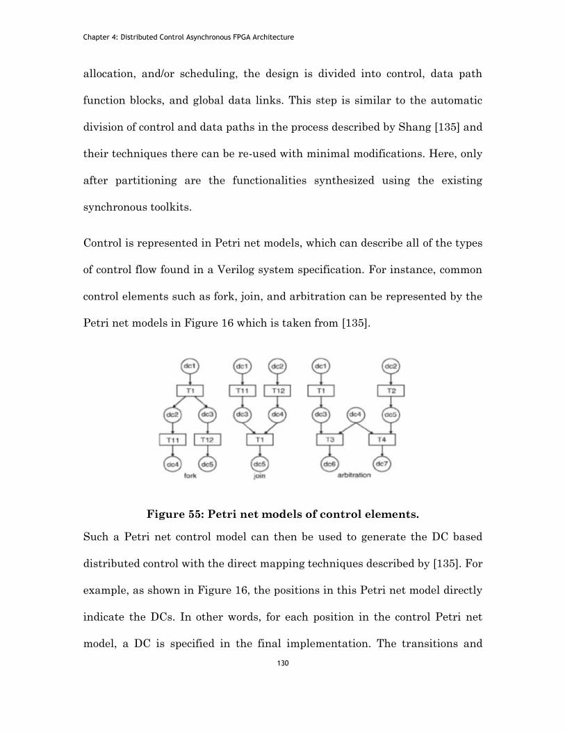
Chapter 4: Distributed Control Asynchronous FPGA Architecture
130
allocation, and/or scheduling, the design is divided into control, data path
function blocks, and global data links. This step is similar to the automatic
division of control and data paths in the process described by Shang [135] and
their techniques there can be re-used with minimal modifications. Here, only
after partitioning are the functionalities synthesized using the existing
synchronous toolkits.
Control is represented in Petri net models, which can describe all of the types
of control flow found in a Verilog system specification. For instance, common
control elements such as fork, join, and arbitration can be represented by the
Petri net models in Figure 16 which is taken from [135].
Figure 55: Petri net models of control elements.
Such a Petri net control model can then be used to generate the DC based
distributed control with the direct mapping techniques described by [135]. For
example, as shown in Figure 16, the positions in this Petri net model directly
indicate the DCs. In other words, for each position in the control Petri net
model, a DC is specified in the final implementation. The transitions and

Chapter 4: Distributed Control Asynchronous FPGA Architecture
131
connection topology among the DC positions are implemented through the SET
and RESET logic of the DCs and the interconnections between them.
The data path function blocks can be similarly derived through a step of colour
Petri net modelling [143]. Once the general function blocks have been
synthesized, they need to be refined based on the FPGA’s granularity for
partitioning, depending on the PLE and cluster sizes. This is not available
directly [143]. However, this is a standard step in converting a general VLSI
design to FPGA implementation, and so the same methods can be applied. By
keeping the PLE and cluster sizes of the conventional FPGA, this step is made
straightforward. This is then followed by obtaining the PLE and cluster
circuits using existing FPGA mapping techniques.
The global data interconnect fabric mainly consists of the channels for data
communication. In this design flow it is implemented directly in dual-rail DI
circuits. Their generation is also a straightforward process.
4.8 Summary
This chapter describes the detailed circuit realization of an asynchronous
FPGA architecture. This is different from existing asynchronous FPGA
architectures, and strikes a sensible balance between homogeneity to modern
synchronous FPGA architecture and full asynchrony in places where it matters
most, namely long interconnect links. This approach allows more flexibility in
adjusting levels of DI according to application needs.

Chapter 4: Distributed Control Asynchronous FPGA Architecture
132
This approach retains the single-rail data representation of conventional
FPGAs “in the small” or local cluster. This maximises the reusability of exiting
FPGA logic mapping tools. On the other hand, by introducing delay-
insensitivity “in the large” into the inter-block long data links, the variation
tolerance and latency robustness inherent to asynchrony is provided.
This hybrid structure also provides advantages of both single-rail computation
and dual-rail communication. This is due to the efficient computation with
single-rail and the correct operation across a wide Vdd range from dual-rail
asynchrony.
A number of structural choices were made; for instance, the granularity and
block structures follow current commercial FPGA practice.
The basic building block of the architecture, the programmable logic element
(PLE), has been designed in detail. It includes a number of finer grain
components, including a logic element (LE) inherited directly from current
commercial FPGAs, completion detection circuits and delay matching / data
bundling circuits.
Programmable completion detection and bundling delays in the PLE cater for
functional configurability and variation tolerance. This type of PLE has been
shown to work under widely variable Vdd with reasonable latency and energy
behaviours.

Chapter 4: Distributed Control Asynchronous FPGA Architecture
133
On the next level above, the PLEs are the clusters. The standard cluster has a
David cell (DC) distributed control unit managing the operations of the PLEs
in a cluster. This asynchronous control fully replaces the intra-cluster clock
system in current commercial FPGAs, providing the complete equivalent
functional set which includes both in parallel and sequential operations of the
PLEs in any possible arrangement.
A design flow for systems in this architecture has been proposed which makes
maximal use of existing asynchronous and FPGA synthesis methods. Case
studies demonstrate the functional capabilities of the architecture. A four-bit
ripple carry full adder showcases the flexibility of intra-cluster DC control. A
further example additionally demonstrates inter-cluster control from a single
DC.
Summary of the performance analysis shows that, although power and
performance can be achieved with the asynchronous wrapper based technique,
the area overhead is still substantial. In particular, the computation logic is
compact compared with existing fine-grain asynchronous FPGA methods, but
the fully dual-rail structure for interconnects required by DI may not be
necessary. In the next chapter, the interconnect structure will be optimised
based on information made possible from recent advancements in variation
instrumentation and variability maps.

Chapter 5: Asynchronously Assisted Logic (AAL) Scheme
134
Chapter 5. Asynchronously Assisted Logic (AAL) Scheme
5.1 Introduction
Asynchronous logic has been shown to be more robust to variations but may
have higher circuit size and power overhead compared to synchronous systems.
However the degree of asynchrony employed in system designs is the result of
a trade-off between resources and functionality, and the complete “DI in the
large” method for interconnects the previous chapter may turn out to be too
expensive. This chapter describes the implementation of Asynchronously
Assisted Logic (AAL) hard circuit blocks into the Xilinx FPGA’s CLB. This
optimised scheme is intended to increase wide range latency variation
tolerances caused by parametric, voltage supply and temperature (PVT)
fluctuations, where there is a need, to improve on the global DI interconnect
structure from the previous chapter. The proposed method suggests deploying
configurable AAL blocks to reinforce only the variation critical paths with the
help of variation maps, rather than to re-map and re-route. The layout level
result shows this method's worst case increase of CLB overall size to be 6.3%
only. If taking account of the interconnect area size into the area calculation,
the area overhead will be significantly lower. This optimised variation aware
strategy retains the structure of the global interconnect resources that occupy
a large proportion of the modern FPGA’s soft fabric, and yet still permits the

Chapter 5: Asynchronously Assisted Logic (AAL) Scheme
135
dual-rail completion-detection (DR-CD) protocol without the need of globally
doubling the interconnect resources. Simulation results with the injection of
voltage variability on both interconnect and computation blocks demonstrate
the robustness of the method. The propose structure also allow
implementations of several popular asynchronous styles to support different
asynchrony at different variability levels. This chapter therefore provides the
best scenario of practical implementation of variation tolerance support logic
in FPGA for tolerating variability.
5.2 Architecture Overview
Asynchronously assisted logic methods is proposed here in order to provide the
appropriate level of variation tolerance and yet still preserving as much of the
modern FPGA overall structure as possible. This approach applies the
asynchrony only when necessary provide the key for significant overhead
minimization.
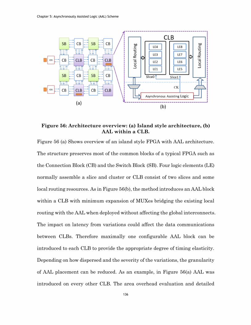
Chapter 5: Asynchronously Assisted Logic (AAL) Scheme
136
Figure 56: Architecture overview: (a) Island style architecture, (b)
AAL within a CLB.
Figure 56 (a) Shows overview of an island style FPGA with AAL architecture.
The structure preserves most of the common blocks of a typical FPGA such as
the Connection Block (CB) and the Switch Block (SB). Four logic elements (LE)
normally assemble a slice and cluster or CLB consist of two slices and some
local routing resources. As in Figure 56(b), the method introduces an AAL block
within a CLB with minimum expansion of MUXes bridging the existing local
routing with the AAL when deployed without affecting the global interconnects.
The impact on latency from variations could affect the data communications
between CLBs. Therefore maximally one configurable AAL block can be
introduced to each CLB to provide the appropriate degree of timing elasticity.
Depending on how dispersed and the severity of the variations, the granularity
of AAL placement can be reduced. As an example, in Figure 56(a) AAL was
introduced on every other CLB. The area overhead evaluation and detailed

Chapter 5: Asynchronously Assisted Logic (AAL) Scheme
137
description of an AAL interface within a CLB will be discussed in the following
sections.
5.3 AAL Architecture Implementation
Figure 57: AAL plugin to Xilinx’s CLB with SLICEL & SCLICEX.
Figure 57 shows a more comprehensive AAL block schematic view and its
interface with the Xilinx’s CLB containing a SLICEL and a SLICEX [144]. To

Chapter 5: Asynchronously Assisted Logic (AAL) Scheme
138
allow interchangeable communication between the synchronous clock and
asynchronous handshaking signal controls, the trigger line (CK) has been
made configurable in a CLB containing an AAL. There are M number data
signal lines for implementation of dual-rail or 1-of-2 protocol. When configured
as dual-rail, the utilization of slices in a CLB will be decreased. However this
design tradeoff was aim to avoid the need of doubling the global interconnect
resources. The output is also interchangeable between single-rail and dual-rail.
There are N lines connecting the AAL dual-rail line to the spare MUXes inputs
in SLICEX. Therefore, the J outputs and I inputs of the original CLB remain
the same. The “ACKo” is the only extra line added in this case.
5.4 Area Overhead Calculation
Figure 58 Area calculation of CLB with AAL.
The implementation of this design is in UMC-90nm CMOS technology and
evaluated the area overhead of the AAL with a CLB containing a Xilinx’s
SLICEL and SLICEX. Both slices containing 6-inputs lookup table (LUTs) but

Chapter 5: Asynchronously Assisted Logic (AAL) Scheme
139
the more complex structure, SLICEL (20736µm2) takes more layout area
compared to SLICEX (19600 µm2). The AAL occupies a layout area of 2704 µm2
out of the total CLB size of 43040 µm2. The area overhead of the AAL in this
case is only 6.3%. If the more complex SLICEM [144] was chosen, the ratio will
reduce further.
Table 9: Overhead of various asynchronous schemes.
Architecture Wrapper
Type
LUTs/
Wrapper
I/O Overhead
Fine-Grain
AFPGA[6, 95]
Fine 1 >4x
Distributed Control AFPGA[69] Medium 4 2x
AAL (this work) Coarse 8 Same + 1
Table 9 shows the overhead comparison between different asynchronous
FPGAs architectures. The fine-grained architecture provides every logic
element with a wrapper increasing the size of the global interconnect resources
over 4 times higher. The main advantage of this type of architecture is
potential fine-grain pipelining for high throughput and high reliability. Yet,
the overall overhead in size is too large, reduces the chip functional density
and to some extent negates the technology scaling objective. Distributed
control AFPGA proposed in [69] reduced the overhead to the factor of two with
clustered architecture wrapped four LUTs with a wrapper. The wrapper
consists of dual-rail handshaking logic plus a distributed David Cell (DC)

Chapter 5: Asynchronously Assisted Logic (AAL) Scheme
140
controller. However, this medium grain scheme still doubles the global
interconnect for dual-rail communication. The DC based controller was also
made to be programmable to accommodate multiple combinations of control
logic. Due to the extra-configurable resources, the wrapper occupied about 50%
of the CLB area. This newly proposed scheme use spare resources in the
existing slice structure and are trading the utilization of CLB with
interconnects overhead. The reduced utilization of CLB when AAL are
deployed is acceptable in this context because only the Variation-critical path
(VCP) will be used. This can be achieved with the help of tools that allow the
identification VCPs. The overhead reduction is very significant and makes
more sense as indicated from simulation results in the following sections.
5.5 Multi-Style Handshaking Support
An FPGA’s functional implementation is defined after fabrication. Although
this may make it suffer more from the variability at nanometer scale regime
compared to ASIC design, FPGA provides a unique opportunity to reconfigure
unused resources to mitigate the problem, for example to remap the degraded
computation block to a region that is not used [77, 81]. The re-routing and re-
mapping techniques are interesting and may work well. However, the place
and route process normally takes a lot of time and effort. Even worse, it may
be too late for the system to sense its level of degradation before system starts

Chapter 5: Asynchronously Assisted Logic (AAL) Scheme
141
malfunctioning. We therefore propose to enhance the VCP path with AAL that
is highly tolerant to variation and does not require exhaustive P&R efforts.
The AAL block provides the flexibility to implement various styles of
asynchrony, including single-rail bundled data (SR-BD), dual-rail completion-
detection (DR-CD), and hybrid completion-detection (HB-CD) as needed. The
structure consists of Programmable Completion Detection (PCD) block,
Programmable Handshake Circuit (PCH) and Programmable Delay element
(PD) [69] as shown in Figure 57 and Figure 59.
Figure 59: Dual-Rail Completion-Detection (DR-CD) resources.
Figure 59 shows the resources used when the AAL is configured to the DR-CD
mode. Complete arrival and retrieval of all dual-rail valid input data are
detected by the PCD and PHC for handshaking between AAL blocks. In this
scheme, encoding within the data itself provide the trigger signal “CK”
substituting the global clock. The PDs in between the “CK” are closely matched
with its corresponding slices. Internally delay matching is acceptable as the
variation within a small region is more manageable. Output data from this

Chapter 5: Asynchronously Assisted Logic (AAL) Scheme
142
scheme can be then converted into dual-rail before propagated to the next stage.
Figure 60 show an example implementation of a four stage pipelined 4-phase
DR-CD using AAL.
Figure 60: Four Stages implementation of DR-CD circuit.
In the SR-BD scheme, the handshaking relies closely on the local matched
delay line. Data are remained in single-rail and not used as part of the control;
hence the PCD is not used (Figure 61). This scheme basically replaces the
global CLK trigger line with the locally handshaking CK trigger. The main
benefit of this structure is simplicity in control handshaking and circuit size
that will result in higher operational energy efficiency. Investigation of
throughput vs energy performance of the architecture will be discussed in the
next section. Figure 62 shows an example implementation of this bundled-data
delay matching circuit in four stages.

Chapter 5: Asynchronously Assisted Logic (AAL) Scheme
143
Figure 61: Single-Rail Bundle-Data (SR-BD) resources.
Figure 62 Four Stages implementation of SR-BD circuit.
It is also entirely possible to mix and match these two most popular
asynchronous handshaking protocols through one data path (HB-CD),
depending on where along that path there may be very long interconnects or
where interconnects are compromised by variability. In addition, the global
clock could be passed straight through, which basically reverts the CLB back
to the conventional synchronous behaviour using the switching resources as
shown in Figure 63.
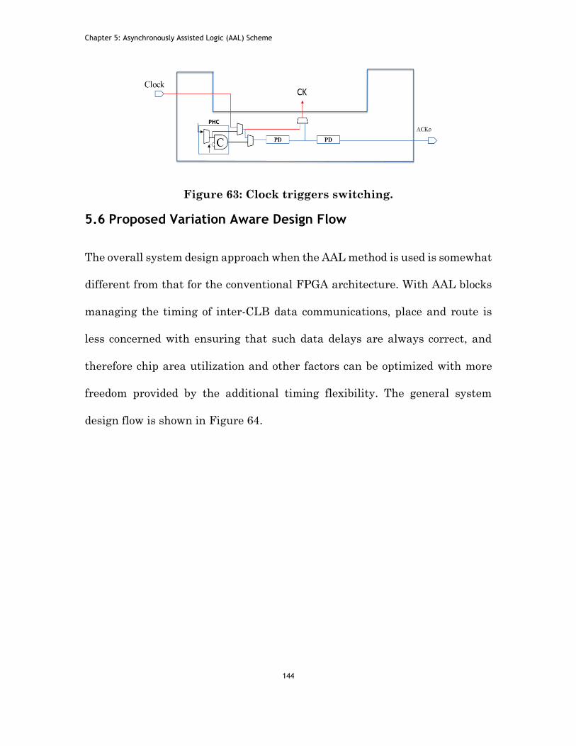
Chapter 5: Asynchronously Assisted Logic (AAL) Scheme
144
Figure 63: Clock triggers switching.
5.6 Proposed Variation Aware Design Flow
The overall system design approach when the AAL method is used is somewhat
different from that for the conventional FPGA architecture. With AAL blocks
managing the timing of inter-CLB data communications, place and route is
less concerned with ensuring that such data delays are always correct, and
therefore chip area utilization and other factors can be optimized with more
freedom provided by the additional timing flexibility. The general system
design flow is shown in Figure 64.

Chapter 5: Asynchronously Assisted Logic (AAL) Scheme
145
Figure 64: Design flow based on variation map.
5.7 Throughput and Operation Energy Study
The AAL method provides the flexibility of configuring inter-CLB data
connections into a full spectrum of different degrees of asynchrony, from
completely depending on the global clock, to single-rail asynchrony based on
timing assumptions, to fully completion-detected DI. Based on theory they
would provide opportunities to trade communication reliability with energy
costs. In this section, we attempt to quantitatively study the energy and
speed/throughput characteristics on the three styles of asynchrony provided
by the AAL method, i.e. everything based on timing assumptions, everything
fully completion detected, and a judicious hybrid of the two.
A case study approach is used in this exploration. First, the FPGA logics are
configured into a 4-bit ripple-carry-adder (4RCA) and follow by an extended
version – a cascade of four 4RCAs (4x4RCA) for a longer critical path. The
examples are selected deliberately for the easy identification of critical paths.

Chapter 5: Asynchronously Assisted Logic (AAL) Scheme
146
5.7.1 Short Critical Path
Figure 65 shows the test setup. Input B of the adder changes (from increment
counter) on every complete computation circle based on the valid “Cout” signal
- the critical path. A closed loop simulation was run for a fixed amount of time
(200ns) and the number of counts from the incremental counter was recorded
together with the overall operational energy.
With a single adder and short critical path, the comparative simulation results
(at the nominal voltage, 1V) are presented in Table 10. The results show that
SR-BD has the highest efficiency (throughput over overall operational energy)
compared to the other two setups. SR-BD performance can also be closely
benchmarked equivalent to the synchronous design for the reason that
matching delay lines were carefully tuned to the data-path. This is similar to
the clock frequency setting based on critical-path in typical synchronous
system design. Further performance investigations with a supply voltage
sweep between 0.4-1.0 volts are shown in Figure 66(a) shows that both (DR-
CD) and (HB-CD) consistently produce lower throughput for relying on the
slow handshaking protocol. The operation energy graph in Figure 66(b) also
indicates, because of the extra dual-rail and completion-detection logics
implemented, the circuits are larger and use more power. However, the HB-
CD design can improve the efficiency.

Chapter 5: Asynchronously Assisted Logic (AAL) Scheme
147
Figure 65: Test setup for 4RCA.
Table 10: Comparison result for short path (4RCA).
Circuits
(4RCA)
Throughput
(counts)
Operational
Energy (pJ)
SR-BD 23 29.49
DR-CD 18 37.28
HB-CD 18 24.64

Chapter 5: Asynchronously Assisted Logic (AAL) Scheme
148
Figure 66: Throughput and energy comparison (Voltage sweep, 0.4 -
1.0v), (a) Throughput (Counts), (b) Operation Energy (pJ).
5.7.2 Long Critical Path
For longer critical path experiment, an an extended version – a cascade of four
4RCAs (4x4RCA) are implemented in four styles. A typical 16-bit ripple-carry-
adder (RCA) as a synchronous design is followed by three asynchronous
implementations of 4x4-bit (RCA). The experiment setup is shown in Figure 67
including an increment counter that records the loop iterations. Same
incremental counter used for input data B. This setup is common to all the four
mentioned examples.

Chapter 5: Asynchronously Assisted Logic (AAL) Scheme
149
Figure 67: Test setup for 16RCA and 4x4RCA.
The same test vector is applied onto all four designs and fixed time (200ms).
Close loop stimulations were run to measure the throughput/counts and
average power performances. Results of the simulation are presented in Table
11: Throughput and energy performance. Note that, in the single-rail delay-
matching (SR-DM) synchronous 16-bit configuration, the 16-bit RCA’s critical
path delay line is carefully tuned to match the synchronous clock speed
representation.
Table 11: Throughput and energy performance.
no Circuits Throughput
(Counts)
Operation
Energy (pJ)
1. Single-Rail Delay-Matching
(SR-DM) (Non-Pipeline)
6 22.63
2. Single-Rail Bundle-Data
(SR-BD)
15 52.27
3. Dual-Rail Completion-Detection (DR-CD) 15 81.79
Chapter 5: Asynchronously Assisted Logic (AAL) Scheme
150
4. Hybrid Mix-Rail
Completion-Detection
(HB-CD) (Carry Chain Only)
15 66.53
The maximum count achieved by SR-DM is 6 with an energy consumption of
22.63pJ. In the 4x4-bit configurations, higher throughput was achieved (15
counts). This is due to the pipelined natural of the circuits. DR-CD design used
highest energy because of fully dual-rail completion detection scheme and the
SR-BD uses much lesser energy for the same throughput. However, this
scheme relies more on timing assumption, and may not be as robust as DR-CD.
HB-CD, on the other hand, reduces total operation energy for maintaining the
same throughput. In this case, a hybrid approach may be beneficial provided
the critical path is carefully determined based on a somewhat accurate
variation map – full accuracy is only needed for the data lines covered by
timing assumptions. A hybrid asynchronous control of data communication
between CLBs is exactly where the AAL method excels.
5.8 Variability Study
In addition to manufacturing process variations, it is also crucial to account for
potential FPGA operation mode variations post-configuration such as
fluctuations of voltage and temperature. In this section we study how the
addition of asynchrony might make FPGA circuits more tolerant to voltage
variations.
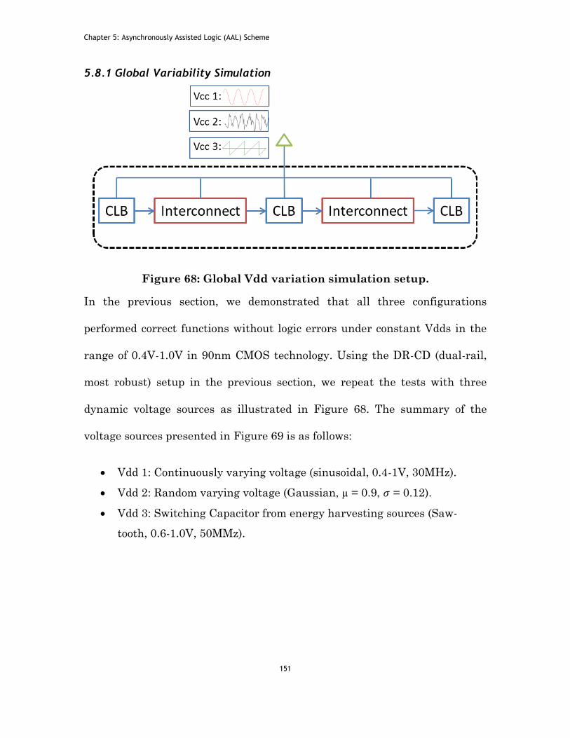
Chapter 5: Asynchronously Assisted Logic (AAL) Scheme
151
5.8.1 Global Variability Simulation
Figure 68: Global Vdd variation simulation setup.
In the previous section, we demonstrated that all three configurations
performed correct functions without logic errors under constant Vdds in the
range of 0.4V-1.0V in 90nm CMOS technology. Using the DR-CD (dual-rail,
most robust) setup in the previous section, we repeat the tests with three
dynamic voltage sources as illustrated in Figure 68. The summary of the
voltage sources presented in Figure 69 is as follows:
Vdd 1: Continuously varying voltage (sinusoidal, 0.4-1V, 30MHz).
Vdd 2: Random varying voltage (Gaussian, µ = 0.9, 𝜎 = 0.12).
Vdd 3: Switching Capacitor from energy harvesting sources (Saw-
tooth, 0.6-1.0V, 50MMz).
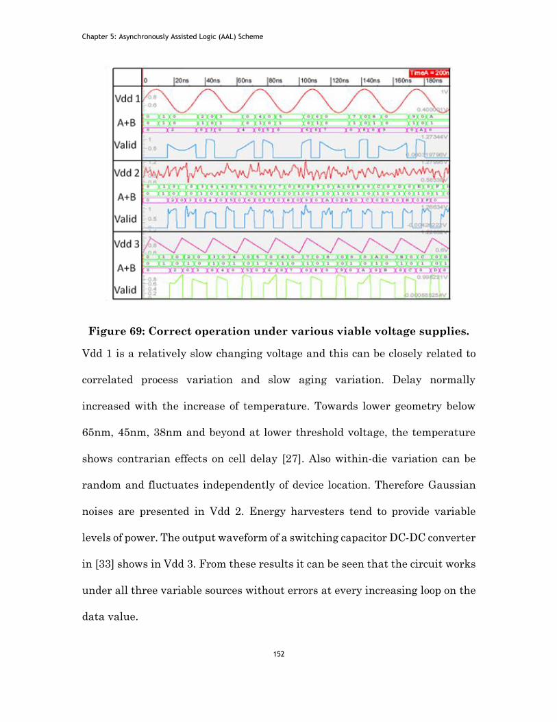
Chapter 5: Asynchronously Assisted Logic (AAL) Scheme
152
Figure 69: Correct operation under various viable voltage supplies.
Vdd 1 is a relatively slow changing voltage and this can be closely related to
correlated process variation and slow aging variation. Delay normally
increased with the increase of temperature. Towards lower geometry below
65nm, 45nm, 38nm and beyond at lower threshold voltage, the temperature
shows contrarian effects on cell delay [27]. Also within-die variation can be
random and fluctuates independently of device location. Therefore Gaussian
noises are presented in Vdd 2. Energy harvesters tend to provide variable
levels of power. The output waveform of a switching capacitor DC-DC converter
in [33] shows in Vdd 3. From these results it can be seen that the circuit works
under all three variable sources without errors at every increasing loop on the
data value.

Chapter 5: Asynchronously Assisted Logic (AAL) Scheme
153
5.8.2 Interconnects Variability Simulation
In previous section [145], the robustness of the design with global Vdd
variation under three variable power supply sources was demonstrated. In this
section, we going to investigate the voltage variability effects on interconnect
latency and it’s potential impact on the correct operation as illustrated in
Figure 70 In FPGAs, a large proportional of the fabric are made of interconnect
blocks. Variations in interconnect could dominate the global system
performance. This section study the structure performance under gradual and
random variable voltages presented in the global interconnect.
Figure 70: Mixed constant Vcc on CLB and variable Vdd on
interconnect simulation.
The most robust DR-CD implementation in the previous section was reused
but with all interconnects replaced with analogue models that are made of non-
standard cell inverter chains. The simulation was done in the mixed signal
mode – all CLBs are using standard cell with fix 1V Vcc supply, while
interconnects used custom cells and are powered with variable Vdd supplies.
The result in Figure 71 shows the correct operation of adder under two variable
voltage sources: Vdd1, a constantly changing voltage between 0.5-1.1V at
Chapter 5: Asynchronously Assisted Logic (AAL) Scheme
154
25MHz with a sinusoidal shape, and Vdd2, a random variable voltage source
with Gaussian distribution (µ = 0.9V, 𝜎 =0.12V).
Variations in the supply voltage result in timing variations of the interconnect
line. Both data and control lines that are connected through the global
resources will be affected. However, it can be seen that the circuit works under
both variable sources without errors with the correct output sum value on
every cycle. The validity of the data was aligned with the “Valid” signal from
the output of the dual-rail completion-detection block sampling at the legit
output values and not spacers.
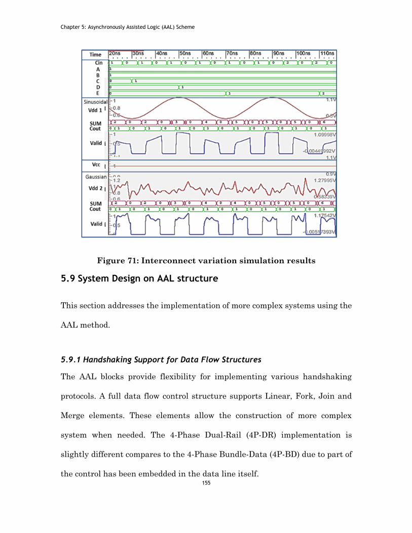
Chapter 5: Asynchronously Assisted Logic (AAL) Scheme
155
Figure 71: Interconnect variation simulation results
5.9 System Design on AAL structure
This section addresses the implementation of more complex systems using the
AAL method.
5.9.1 Handshaking Support for Data Flow Structures
The AAL blocks provide flexibility for implementing various handshaking
protocols. A full data flow control structure supports Linear, Fork, Join and
Merge elements. These elements allow the construction of more complex
system when needed. The 4-Phase Dual-Rail (4P-DR) implementation is
slightly different compares to the 4-Phase Bundle-Data (4P-BD) due to part of
the control has been embedded in the data line itself.
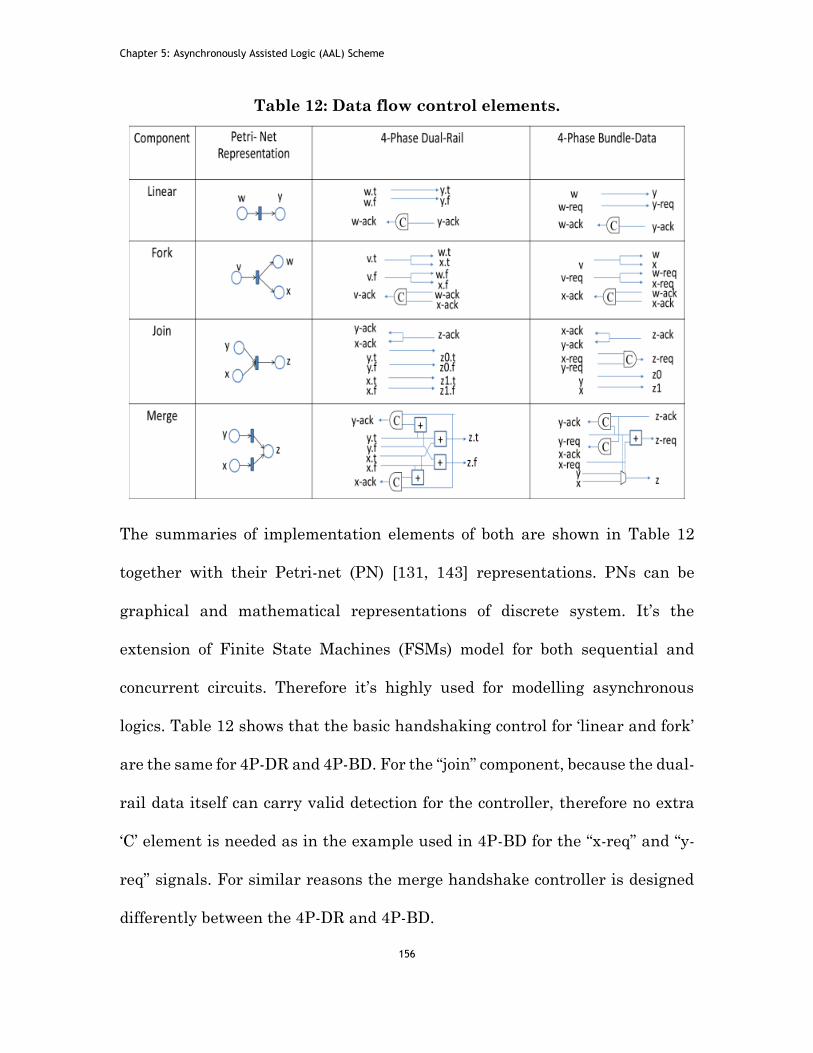
Chapter 5: Asynchronously Assisted Logic (AAL) Scheme
156
Table 12: Data flow control elements.
The summaries of implementation elements of both are shown in Table 12
together with their Petri-net (PN) [131, 143] representations. PNs can be
graphical and mathematical representations of discrete system. It’s the
extension of Finite State Machines (FSMs) model for both sequential and
concurrent circuits. Therefore it’s highly used for modelling asynchronous
logics. Table 12 shows that the basic handshaking control for ‘linear and fork’
are the same for 4P-DR and 4P-BD. For the “join” component, because the dual-
rail data itself can carry valid detection for the controller, therefore no extra
‘C’ element is needed as in the example used in 4P-BD for the “x-req” and “y-
req” signals. For similar reasons the merge handshake controller is designed
differently between the 4P-DR and 4P-BD.

Chapter 5: Asynchronously Assisted Logic (AAL) Scheme
157
Following subsection will demonstrate the building of a 4P-BD sub function
with most of the components listed in the Table 12
5.9.2 Booth Multiplier Case Study
This section describes a Booth's multiplication algorithm system in the
proposed AAL structure with the above-mentioned handshaking components.
Figure 72 shows the block diagram of a four by four-signed binary
multiplication. This structure is of interest for study because the adder
example used for performance study in section IV can be reused with minimum
alteration as shown the 9-bit adder in the diagram. Also Booth’s multiplier
provides balance between speed and area utilization using repetition adding
and shifting. The multiplier value is first extended and stored in register
“A_reg” and its two’s complemented value is stored in “S_reg”. Conditioned by
the last two bits of the product accumulator register “M”, addition or
subtraction will be performed between the multiplicand “P_reg” with the
“A_reg” or “S_reg” within a set number of iteration controlled by a counter.

Chapter 5: Asynchronously Assisted Logic (AAL) Scheme
158
Figure 72: Block diagram of Booth multiplier.
Figure 73 : Petri-net representation of booth multiplier control flow.
Figure 74: Simplified SR-BD handshaking diagram for Booth
multiplier.

Chapter 5: Asynchronously Assisted Logic (AAL) Scheme
159
Figure 73 shows the data flow diagram using PN representation for the
implemented the above Booth’s Multiplier and matching with components in
Table 12: Data flow control elements, the simplified handshaking building
block on CLB with AAL block can easily be constructed as in Figure 74.
Figure 75: Simulation waveform of Booth multiplier
implementations.
The simulation result using Cadence tools is shown in Figure 75. The
waveforms show a multiplication of two 4-bit numbers (m = 3 and r = -4). The
manipulated equivalent of ‘m’ and its two’s complement value are stored in
A_reg and S_reg individually as 9-bit data in hexadecimal format. For ‘r’, the
manipulated value is store in P_reg. The number of iterations loop is
determined by the bit length of value ‘r’. In this case, after four counts, a correct
product value of “-12” is produced demonstrating the correct operation.

Chapter 5: Asynchronously Assisted Logic (AAL) Scheme
160
5.10 Summary
This chapter aims to present the integration of robust AAL block into existing
Xilinx FPGA architecture. The proposed structure does not increase the
interconnect resource much as compared to typical asynchronous FPGAs that
would at least double the interconnect resources to support dual-rail
connection. The die overhead calculation on layout level shows that
incorporating AAL into a Xilinx’s CLB with SLICEM & SLICEX only incurred
6.3% of die area overhead at the maximum. The AAL design allows the
configuration of different styles and degrees of asynchrony for data links
between CLBs, depending on specific requirements. Quantitative case studies
using a 16-bit RCA also show that potential throughput improvements can be
achieved when AAL handshake can be pipelined. In addition, simulations also
show that the power efficiency can be improved with the hybrid implantation
of DR-CD protocol on critical path only and keeping the rest single-rail. The
most robust form of asynchrony is shown to be reliable under radical timing
variation caused by varying voltages on interconnects. A case study of Booth’s
multiplier shows the feasibility of building a more complex system on AAL
structure.
With the AAL hardware support and potential variation aware design flow, a
more practical and industry acceptable scenario would be more feasible.
Standard industrial design flow assumes only one set of bitstream needs to be

Chapter 5: Asynchronously Assisted Logic (AAL) Scheme
161
generated for a large batch of chips implementation. Thus, compared with
traditional variation aware techniques that require expensive computation for
re-routing and re-mapping the whole design on the basis of a unique variation
map for each chip, AAL technique may avoid this. Summary of such approach
will be discussed in the final conclusion chapter.

Chapter 6: Conclusion
162
Chapter 6. Conclusion
6.1 Summary of Thesis
This thesis presents a set of practical techniques for incorporation
asynchronous logic into modern FPGAs architectures as a method of dealing
with the increasing variability issues face by current and future sub-
nanometer technologies.
This approach based on Asynchronously-Assisted Logic (AAL) makes it
possible to provide the right degree of asynchronous hard microcircuit while
keeping most the conventional FPGA structure intact. The AAL method
facilitates the architecture with hard asynchronous components that is
distributed around the fabric, thus equips the architecture with robust
hardware resources to combat against timing variation. (Traditional methods
either modified the architecture greatly for fully asynchronous implementation
or betting on P&R tools to impose asynchrony logic on exiting FPGA
architecture, which is not ideal).
On the way towards the AAL approach, a hybrid FPGA architecture that wraps
conventional synchronous FPGA logic blocks with distributed asynchronous
control based on David’s cell options was developed. This approach preserves
the single-rail data representation of current FPGAs “in the small”, it is
possible for designers to use existing FPGA logic mapping tools in block design.

Chapter 6: Conclusion
163
By introducing delay-insensitivity “in the large” into the inter-block long data
links, the variation tolerance and latency robustness inherent to asynchrony
is provided. A number of structural choices were evaluated including the
granularity and block structures. This provided the foundation on which the
AAL approach was developed.
Several existing solutions to the variability problem exploit the reconfiguration
features of FPGAs. For example the late binding techniques suggest
performing part of the mapping and routing process as late as possible
leveraging the unique variation characterising of each chip. The proposed AAL
method provides a complementary solution to existing variation aware late
binding approach where delay characterisation is first performed and then
techniques such the region relocation, logic replacement and path rerouting
techniques can be applied, with AAL it will be reinforcement. The
reinforcement strategy suggests retaining the placement and routing and
supporting the variation critical regions or paths variation robust hardware
components thus minimising the effort for recalculating the new configuration
in FPGA.
Implemented on Faraday 90nm standard cell library on Cadence tools, the
worst case increase of CLB overhead in the layout level is 6.3% when
integrated into Xilinx’s vertex 6 architecture. Considering the interconnect
resources that occupy the biggest slice of the FPGA fabric, the overall size

Chapter 6: Conclusion
164
increase for consolidating the AAL block could be significantly lower at around
2%.
Furthermore, the AAL resources support multi-style asynchronous
implementation in tolerating wide range of timing variability. As reviewed in
chapter 2, the choice of asynchronous implementation style is fixed during the
specification process motivated mainly for speed or power performance. This
reduced the flexibility for tolerating wide range of variability. For example the
bundle data approach is more energy efficient but because it relies heavily on
the timing assumption, this makes it not suitable to deal with spatial and
random variation. Alternatively, a highly-pipelined 4phase dual-rail (4P-DR)
structure choice is made; the robustness of the architecture will be trading-off
with the huge area overhead.
The AAL approach avoids the need to globally double the interconnect
resources to permit either of these handshaking implementation and
combination benefit of SI/DI schemes. The adjustment is made by reduces the
logic utilisation of a CLB if AAL is deployed. This is not unreasonable at the
assumption that AAL will only be deployed on a few targeted variation-critical
paths (VCPs). This technique has been successfully implemented with a case
study demonstrated in chapter 5.

Chapter 6: Conclusion
165
6.2 Future Work
This thesis presents an approach for the practical implementation of
asynchronous logic to assist with the growing variability issue in digital circuit
design. There are several areas in which this approach could be extended.
6.1.1 Variation Aware Design Flow with Consolidated Variation Map
The variability issue will inevitably impact the reliability and timing yield of
future generation FPGA. In this thesis a hardware optimized solution has been
proposed, however this needs to be supported by a design flow or automated
tools. With the assumption of mature off-line and online sensing techniques,
each chip can be characterised and treated differently. A few variation aware
techniques were discussed in chapter 2, however in all these papers, either
only the process variability is considered or in some, the run-time thermal
variation. Considering one single variation map may not give a comprehensive
view of the variability problem. It is therefore important to develop an
algorithm that consolidates both process and run-time variation maps for a
more realistic variation aware flow.
6.1.2 Cross Domain and GALS Scheme Study
Proposed AAL technique suggests multiple asynchronous handshaking
protocols can be collaboratively worked together. However detail study needs
to be performed for seamless integration to avoid complex intermingle of
different protocol in a design. Also, data transfer between asynchronous and
Chapter 6: Conclusion
166
synchronous domain would be expected in such implementation. This is in
some degree make the system similar to the heterogeneous GALS and
multiple-clock-domain system. Mixed timing domain in a system makes the
timing-closure and global-clock distribution difficult to achieve. One of the
solutions to deal with the global and local communication speed mismatch is
to make them insensitive to the latency. The Globally Asynchronous Locally
Synchronous (GALS) methodology does not enforce globally synchronized
clocks. Instead, communication between modules occurs asynchronously. This
approach has been popularly used by industry today to implement large SoC
with sub-modules running on different clocks. This trend is expected to extend
into future multi-core processors and NoC system. The proposed AAL
architecture may fit into this paradigm closely. However, the modification and
design of asynchronous and synchronous domain adapter circuits need to be
further explored, especially in terms of balancing throughput and size
overhead.
6.1.3 Silicon Implementation
The motivation and focus of this work is centred on the practical
implementation of FPGA architecture with enhancements for variability. The
architecture circuit has been designed and simulated in the Cadence tools
environment using both UMC-90nm and Faraday 90nm technology. It would
be beneficial, to develop a better sense of context to have the design evaluated
in smaller technology nodes such as 45nm or below if the tools and foundry
Chapter 6: Conclusion
167
library are made available. Also, implementation of the developed architecture
in silicon for further testing and verification would be a natural next step.

Appendixes
168
Appendix A: Abbreviations
2P-DR: 2-Phase Dual-Rail
4P-DR: 4-Phase Dual-Rail
ASIC: Application –Specific Intergraded Circuit
CAD: Computer-Added-Design
CB: Connection Block
CD: Completion Detection
CMP: Chemical Mechanical Polishing
CPLD: Complex Programmable Logic Device
DC: David Cell
DI: Delay Insensitive
DPA: Differential Power Analysis
DR-CD: Dual-Rail Completion-Detection
DR-CD: Dual-Rail Completion-Detection
DSP: Digital-Signal-Processing
DUT: Device-Under-Test
EEPROM: Electrically Erasable Programmable ROM
EMA: Electromagnetic Analysis
FSM: Finite State Machine
FU: Functional-Unit
GALS: Global Asynchronous Locally Synchronous
HB-CD: Hybrid Completion-Detection
HCI: Hot-Carried-Injection
HDL: Hardware Description Language
IoT: Internet-of-Thing
IP: Intellectual Property

Appendixes
169
LC: Logic Cluster
LE: Logic Element
LEDR: Level-Encoded Dual-Rail
LER Line-Edge-Roughness
LUT: Look-Up Table
NBTI: Negative Bias-Temperature Instability
NoC: Network-on-Chip
NRZ: Non-Return-Zero
P&R: Placement and Routing
PAL: Programmable Array Logic
PBTI: Positive Bias-Temperature Instability
PCB: Printed Circuit Board
PCD: Programmable Completion Detection
PD: Programmable Delay
PL: Phase Logic
PLA: Programmable Logic Array
PLD: Programmable Logic Devices
PLE: Programmable Logic Elements
PN Petri-Net
PROM: Programmable Read-Only Memory
PVT: Process, Voltage and Temperature
QDI: Quasi Delay Insensitive
RCA: Ripple-Carry-Adder
RDF: Random-Dopant Fluctuation
RO: Ring oscillator
RTA: Rapid Thermal Annealing
RZ Return-to-Zero
SB: Switching Block
SCA: Side Channel Attack

Appendixes
170
SI: Speed Independent
SoC: System-on-Chip
SPA: Simple Power Attack
SRAM: Atatic-Random-Access-Memory
SR-DM: Single-Rail Direct-Mapping
SR-DM: Single-Rail Delay-Matching
SSTA: Statistical static Timing Analysis
STA: Static Timing Analysis
TDDB: Time Dependent Dielectric Breakdown
VCP: Variation-Critical Path

Appendixes
171
Appendix B: AAL Implementation
Incorporating AAL into Xilinx’s CLB

Appendixes
172
Appendix C: Input Vector for Candence
Input Stimulus “Vector” file sample (Configure LUT
as Adder)
; PLE cd stimuli
; INPUT & DBUS Use BIG_ENDIAN system (LS byte first 0|1|2|3)
; Address use LITTLE_ENDIAN (MSB fist 3|2|1|0)
Radix 1 1 4444 1 4 1 2 2 2
Io i I iiii I I i I I o
vname start WE DBUS<[15:0]> Sel PCD<[3:0]> SW PD1<[1:0]> PD2<[1:0]>
sum<[1:0]>
tunit ns
trise 0.1
tfall 0.1
vih 1
vil 0
vol 0
voh 1
;time start WE DBUS Sel PCD SW PD1 PD2 sum
0 0 0 0000 0 0 0 0 0 0;
10 0 1 6996 0 0 0 x x x; Adder
20 0 0 6996 0 0 0 x x x;
40 0 0 xxxx 0 0 0 0 0 0; Spacer
60 1 0 xxxx 1 F 1 2 2 x;
160 0 0 xxxx 1 F 1 2 2 x;
180 1 0 xxxx 1 F 1 2 2 x;
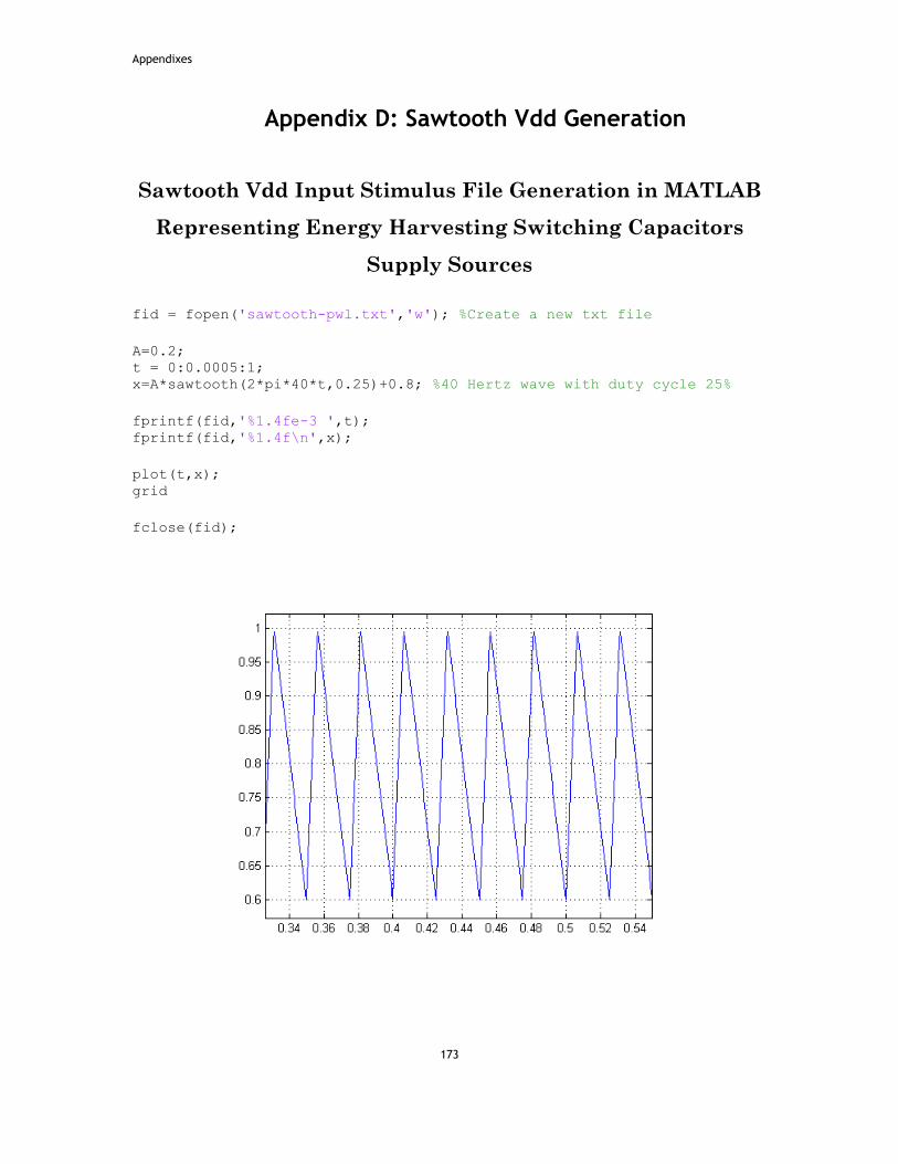
Appendixes
173
Appendix D: Sawtooth Vdd Generation
Sawtooth Vdd Input Stimulus File Generation in MATLAB
Representing Energy Harvesting Switching Capacitors
Supply Sources
fid = fopen('sawtooth-pwl.txt','w'); %Create a new txt file
A=0.2; t = 0:0.0005:1; x=A*sawtooth(2*pi*40*t,0.25)+0.8; %40 Hertz wave with duty cycle 25%
fprintf(fid,'%1.4fe-3 ',t); fprintf(fid,'%1.4f\n',x);
plot(t,x); grid
fclose(fid);

Appendixes
174
Appendix E: Variation Map Generation
Variation Map Generation in MATLAB
%Run in Matlab SimulationTime and TimeIncrement are in %nanoseconds Mean and StDev of Guassian distribution is in V Nominal %voltage is in V
% Example m file run code >> VariationMap(0.9, 0.4);
function out = VariationMap(Mean, StDev)
times = zeros(1,201); xs = zeros(1,201); for i=0:1:200 time=i; x=randn(1)*StDev + Mean; y=randn(1)*StDev + Mean; z= randn(1); times(i+1)=time; xs(i+1)=x; end
subplot(2,1,1) plot(times,xs) subplot(2,1,2) hist(xs,20) [X,Y,Z] = peaks(25); surf(X,Y,Z); out=1; end

References
175
Bibliography
[1] R. Aitken, "Predictive technology for advanced node design exploration," in Designing with Uncertainty - Opportunities & Challenges, Workshop Invited Speacker, 2014.
[2] J. M. Levine, E. Stott, and P. Y. K. Cheung, "Dynamic voltage and frequency scaling with online slack measurement," in Field-Programmable Gate Arrays ACM/SIGDA International Symposium, Monterey, California, USA, 2014, pp. 109-116.
[3] P. Sedcole and P. Y. K. Cheung, "Within-die delay variability in 90nm FPGAs and beyond," in International Conference Field Programmable Technology (ICFPT) 2006, pp. 97-104.
[4] P. Cheung, "Beyond the age of clones," UK Design Forum (UKDF) Workshops 2013.
[5] P. Cheung and P. Sedcole, "Variability & FPGAs - Disaster or Opportunities?," Design, Automation & Test (DATE) Workshop Patent, 2008.
[6] R. Manohar, "Reconfigurable asynchronous logic," in Custom Integrated Circuits Conference (CICC), 2006, pp. 13-20.
[7] K.-L. Chang, J. S. Chang, B.-H. Gwee, and K.-S. Chong, "Synchronous-logic and asynchronous-logic 8051 microcontroller cores for realizing the internet of things: a comparative study on dynamic voltage scaling and variation effects," IEEE Journal Emerging and Selected Topics in Circuits and Systems, vol. 3, pp. 23-34, 2013.
[8] M. Jelodari and J. D. Garside, "High level synthesis of GALS systems," in Designing with Uncertainty - Opportunities & Challenges Workshop vol. 2014, ed, 2014.
[9] I. Kuon, R. Tessier, and J. Rose, "FPGA Architecture: Survey and Challenges," Found. Trends Electron. Des. Autom., vol. 2, pp. 135-253, 2008.
[10] N. J. Rochelle, "Monolithic Memories announces: a revolution in logic design: Introductory advertisement on PAL (Programmable Array Logic)," 1978.
[11] G. E. Moore, "Cramming more components onto integrated circuits," Proceedings of the IEEE, vol. 86, pp. 82-85, 1998.
[12] Microsemi Antifuse FPGAs. Available: http://www.microsemi.com/products/fpga-soc/antifuse-fpgas
[13] D. Zacher. Using prescision to design Rad-hard Actel devices [Online]. Available: http://www.pldworld.com/_hdl/2/resources/leo2precision/html/pdfs/actel_rad.pdf
[14] T. R. Kuphaldt, Lesson In Eletric Circuits vol. IV-Digital Chapter 16 Principle of Digital Computing, 200-2008.

References
176
[15] I. Kuon and J. Rose, "Measuring the gap between FPGAs and ASICs," IEEE Transactions on Computer-Aided Design of Integrated Circuits and Systems, vol. 26, pp. 203-215, 2007.
[16] H. Parandeh-Afshar and P. Ienne, "Measuring and reducing the performance gap between embedded and soft multipliers on FPGAs," in International Conference on Field Programmable Logic and Applications (FPL), 2011, pp. 225-231.
[17] FPGA vs. ASIC. Available: http://www.xilinx.com/fpga/asic.htm [18] P. Wilson, Design recipes for FPGAs: Newnes, 2007. [19] S. Borkar, T. Karnik, S. Narendra, J. Tschanz, A. Keshavarzi, and V. De,
"Parameter variations and impact on circuits and microarchitecture," in 40th Annual Design Automation Conference, Anaheim, CA, USA, 2003, pp. 338-342.
[20] A. Bansal and R. M. Rao, "Variations: Sourcecs and characterization," in Low-Power Variation-Tolerant Design in Nanometer Silicon, Swarup. Bhunia and Siabal. Mukhopadhyay, Eds., ed: Springer, 2011.
[21] A. Asenov, S. Kaya, and A. R. Brown, "Intrinsic parameter fluctuations in decananometer MOSFETs introduced by gate line edge roughness," IEEE Transactions on Electron Devices, vol. 50, pp. 1254-1260, 2003.
[22] S. Ghosh and K. Roy, "Parameter variation tolerance and error resiliency: New design paradigm for the nanoscale Era," Proceedings of the IEEE, vol. 98, pp. 1718-1751, 2010.
[23] S. Bhunia and S. Mukhopadhyay, Low-Power Variation-Tolerant Design in Nanometer Silicon: Springer, 2011.
[24] J. A. Walker, M. A. Trefzer, S. J. Bale, and A. M. Tyrrell, "PAnDA: A reconfigurable architecture that adapts to physical substrate variations," IEEE Transactions on Computers, vol. 62, pp. 1584-1596, 2013.
[25] S. K. Saha, "Modeling process variability in scaled CMOS technology," IEEE Design & Test of Computers, vol. 27, pp. 8-16, 2010.
[26] A. Asenov, "Random dopant induced threshold voltage lowering and fluctuations in sub-0.1um MOSFET's: A 3-D "atomistic" simulation study," Electron Devices, IEEE Transactions, vol. 45, pp. 2505-2513, 1998.
[27] M. Ruben. (2012). How to close timing with hundreds of multi-mode/multi-corner views. Available: http://www.eejournal.com/archives/articles/20121206-cadence/
[28] S. Herbert and D. Marculescu, "Variation-aware dynamic voltage/frequency scaling," in IEEE 15th International Symposium on High Performance Computer Architecture (HPCA), 2009, pp. 301-312.
[29] M. Wirnshofer, Variation-aware adaptive voltage scaling for digital CMOS circuits: Springer Dordrecht Heidelberg New York London, 2013.
[30] A. Nahapetian, P. Lombardo, A. Acquaviva, L. Benini, and M. Sarrafzadeh, "Dynamic reconfiguration in sensor networks with regenerative energy sources," in Design, Automation & Test in Europe Conference & Exhibition (DATE), 2007, pp. 1-6.
[31] ARVENI. Available: http://www.arveni.fr/en/

References
177
[32] A. Yakovlev. Energy-modulated computing [Online]. Available: http://async.org.uk/tech-reports/NCL-EECE-MSD-TR-2010-167.pdf
[33] X. Zhang, D. Shang, F. Xia, H. S. Low, and A. Yakovlev, "A hybrid power delivery method for asynchronous loads in energy harvesting systems," in IEEE 10th International New Circuits and Systems Conference (NEWCAS), 2012, pp. 413-416.
[34] F. Xia, A. Mokhov, A. Yakovlev, A. Iliasov, A. Rafiev, and A. Romanovsky, "Adaptive resource control in multi-core systems," Newcastle University NCL-EEE-MICRO-TR-2013-183, 2013.
[35] A. Mokhov, D. Sokolov, and A. Yakovlev, "Adapting Asynchronous Circuits to Operating Conditions by Logic Parametrisation," in Asynchronous Circuits and Systems (ASYNC), 2012 18th IEEE International Symposium on, 2012, pp. 17-24.
[36] F. Xia, A. Mokhov, Y. Zhou, Y. Chen, I. Mitrani, D. Shang, et al., "Towards power-elastic systems through concurrency management," Computers & Digital Techniques, IET, vol. 6, pp. 33-42, 2012.
[37] A. Mokhov, M. Rykunov, D. Sokolov, and A. Yakovlev, "Design of Processors with Reconfigurable Microarchitecture," Low Power Electronics and Applications, pp. 26-43, 2014.
[38] M. Rykunov, "Design of asynchronous microprocessor for power proportionality," PhD, School of Electrical and Electronic Engineering, Newcastle University, 2014.
[39] T. Mizuno, J. Okumtura, and A. Toriumi, "Experimental study of threshold voltage fluctuation due to statistical variation of channel dopant number in MOSFET's," Electron Devices, IEEE Transactions, vol. 41, pp. 2216-2221, 1994.
[40] K. Agarwal, F. Liu, C. McDowell, S. Nassif, K. Nowka, M. Palmer, et al., "A test structure for characterizing local device mismatches," in Symposium on VLSI Circuits, Digest of Technical Papers, 2006, pp. 67-68.
[41] F. Stellari, P. Song, A. J. Weger, and D. L. Miles, "Mapping systematic and random process variations using Light emission from Off-State Leakage," in IEEE International Reliability Physics Symposium 2009, pp. 640-649.
[42] A. N. Nowroz and S. Reda, "Thermal and power characterization of field-programmable gate arrays," in Proceedings of the 19th ACM/SIGDA international symposium on Field programmable gate arrays, Monterey, CA, USA, 2011, pp. 111-114.
[43] M. Bhushan, M. B. Ketchen, S. Polonsky, and A. Gattiker, "Ring oscillator based technique for measuring variability statistics," in IEEE International Conference on Microelectronic Test Structures (ICMTS), 2006, pp. 87-92.
[44] I. A. K. M. Mahfuzul, A. Tsuchiya, K. Kobayashi, and H. Onodera, "Variation-sensitive monitor circuits for estimation of Die-to-Die process variation," in IEEE International Conference on Microelectronic Test Structures (ICMTS), 2011, pp. 153-157.
[45] K. M. Zick and J. P. Hayes, "On-line sensing for healthier FPGA systems," in Proceedings of the 18th Annual ACM/SIGDA International Symposium

References
178
on Field Programmable Gate Arrays, Monterey, California, USA, 2010, pp. 239-248
[46] W. Xiaoxiao, M. Tehranipoor, and R. Datta, "Path-RO: A novel on-chip critical path delay measurement under process variations," in IEEE/ACM International Conference on Computer-Aided Design (ICCAD) 2008, pp. 640-646.
[47] S. Lopez-Buedo, J. Garrido, and E. Boemo, "Thermal testing on programmable logic devices," in IEEE International Symposium on Circuits and Systems (ISCAS), 1998, pp. 240-243 vol.2.
[48] N. Dahir, G. Tarawneh, T. Mak, R. Al-Dujaily, and A. Yakovlev, "Design and implementation of dynamic thermal-adaptive routing strategy for networks-on-chip," in 22nd Euromicro International Conference on Parallel, Distributed and Network-Based Processing (PDP), 2014, pp. 384-391.
[49] G. Tarawneh, T. Mak, and A. Yakovlev, "Intra-chip physical parameter sensor for FPGAS using flip-flop metastability," in International Conference on Field Programmable Logic and Applications (FPL), 2012, pp. 373-379.
[50] P. Y. K. Cheung. On-silicon instrumentation - An approach to alleviate the variability problem [Online]. Available: http://www.panda.ac.uk/workshop/
[51] S. Mukhopadhyay, K. Keunwoo, K. A. Jenkins, C. Ching-Te, and K. Roy, "An On-Chip test structure and digital measurement method for statistical characterization of local random variability in a process," IEEE Journal of Solid-State Circuits, vol. 43, pp. 1951-1963, 2008.
[52] R. Rao, K. A. Jenkins, and J.-J. Kim, "A completely digital on-chip circuit for local-random-variability measurement," in IEEE International Solid-State Circuits Conference ( ISSCC), Digest of Technical Papers, 2008, pp. 412-623.
[53] R. Rao, K. A. Jenkins, and J.-J. Kim, "A local random variability detector with complete digital On-Chip measurement circuitry," IEEE Journal of Solid-State Circuits, vol. 44, pp. 2616-2623, 2009.
[54] S. Lopez-Buedo, J. Garrido, and E. Boemo, "Thermal testing on reconfigurable computers," IEEE Design & Test of Computers, vol. 17, pp. 84-91, 2000.
[55] Haile. Yu, Qiang. Xu, and P. H. W. Leong, "Fine-grained characterization of process variation in FPGAs," in International Conference on Field-Programmable Technology (FPT), 2010, pp. 138-145.
[56] E. Stott, A, J. S. J. Wong, P. Sedcole, and P. Y. K. Cheung, "Degradation in FPGAs: measurement and modelling," in Proceedings of the 18th Annual ACM/SIGDA International Symposium on Field Programmable Gate Arrays, Monterey, California, USA, 2010, pp. 229-238
[57] S. Reda, R. J. Cochran, and A. N. Nowroz, "Improved thermal tracking for processors using hard and soft sensor allocation techniques," IEEE Transactions on Computers, vol. 60, pp. 841-851, 2011.
[58] J. S. J. Wong, P. Sedcole, and P. Y. K. Cheung, "Self-Measurement of combinatorial circuit delays in FPGAs," ACM Trans. Reconfigurable Technol. Syst., vol. 2, pp. 1-22, 2009.

References
179
[59] J. S. J. Wong and P. Y. K. Cheung, "Improved delay measurement method in FPGA based on transition probability," in Proceedings of the 19th ACM/SIGDA international symposium on Field programmable gate arrays, Monterey, CA, USA, 2011, pp. 163-172
[60] J. S. J. Wong and P. Y. K. Cheung, "Timing measurement platform for arbitrary black-box circuits based on transition probability," IEEE Transactions on Very Large Scale Integration (VLSI) Systems, vol. 21, pp. 2307-2320, 2013.
[61] N. Mehta and A. DeHon, "Variation and aging tolerance in FPGAs," in Low-Power Variation-Tolerant Design in Nanometer Silicon, S. Bhunia and S. Mukhopadhyay, Eds., ed: Springer US, 2011, pp. 365-380.
[62] Ho-Yan. Wong, Lerong. Cheng, Yan. Lin, and Lei. He, "FPGA device and architecture evaluation considering process variations," in IEEE/ACM International Conference on Computer-Aided Design (ICCAD) 2005, pp. 19-24.
[63] J. S. J. Wong, P. Sedcole, and P. Y. K. Cheung, "A transition probability based delay measurement method for arbitrary circuits on FPGAs," in ICECE Technology, 2008. FPT 2008. International Conference on, 2008, pp. 105-112.
[64] I. Kuon and J. Rose, "Automated transistor sizing for FPGA architecture exploration," in 45th ACM/IEEE Design Automation Conference (DAC), 2008, pp. 792-795.
[65] J. Sparsø and S. Furber, Principles of asynchronous circuit design, 1st ed.: Springer, 2002.
[66] A. J. Martin, "Compiling communicating processes into delay-insensitive VLSI circuits," Distributed Computing, vol. 1, pp. 226-234, 1986/12/01 1986.
[67] T.-A. Chu, "Synthesis of self-timed VLSI circuits from graph-theoretic specifications," PhD, Massachusetts Institute of Technology. Dept. of Electrical Engineering and Computer Science., Massachusetts Institute of Technology, 1987.
[68] D. Shang, F. Xia, and A. Yakovlev, "Asynchronous FPGA architecture with distributed control " in IEEE International Symposium Proceedings of Circuits and Systems, 2010, pp. 1436-1439.
[69] H. S. Low, D. Shang, F. Xia, and A. Yakovlev, "Variation tolerant AFPGA architecture," presented at the 17th IEEE International Symposium Asynchronous Circuits and Systems, Ithaca, NY, 2011.
[70] P. Sedcole and P. Y. K. Cheung, "Parametric yield in FPGAs due to within-die delay variations: a quantitative analysis," in Proceedings of the 2007 ACM/SIGDA 15th international symposium on Field programmable gate arrays, Monterey, California, USA, 2007.
[71] M. Yohei, H. Masakazu, K. Takashi, T. Toshiyuki, N. Tadashi, S. Toshihiro, et al., "Performance and yield enhancement of FPGAs with within-die variation using multiple configurations," in Proceedings of the 2007 ACM/SIGDA 15th international symposium on Field programmable gate arrays, Monterey, California, USA, 2007.

References
180
[72] L. Cheng, J. Xiong, L. He, and M. Hutton, "FPGA performance optimization via chipwise placement considering process variations," in International Conference on Field Programmable Logic and Applications (FPL), 2006, pp. 1-6.
[73] Y. Lin, M. Hutton, and L. He, "Placement and timing for FPGAs considering variations," in International Conference on Field Programmable Logic and Applications (FPL), 2006, pp. 1-7.
[74] Y. Lin, L. He, and M. Hutton, "Stochastic physical synthesis considering prerouting interconnect uncertainty and process variation for FPGAs," IEEE Transactions on Very Large Scale Integration (VLSI) Systems, vol. 16, pp. 124-133, 2008.
[75] A. Kumar and M. Anis, "FPGA design for timing yield under process variations," IEEE Transactions on Very Large Scale Integration (VLSI) Systems, vol. 18, pp. 423-435, 2010.
[76] S. Sivaswamy and K. Bazargan, "Statistical analysis and process variation-aware routing and skew assignment for FPGAs," ACM Transactions on Reconfigurable Technology System, vol. 1, pp. 1-35, 2008.
[77] P. Sedcole and P. Y. K. Cheung, "Parametric yield modeling and simulations of FPGA circuits considering within-die delay variations," ACM Transactions on Reconfigurable Technology System, vol. 1, pp. 1-28, 2008.
[78] V. Betz, J. Rose, and A. Marquardt, Architecture and CAD for deep-submicron FPGAs. Boston: Kluwer Academic, 1999.
[79] E. Stott and P. Y. K. Cheung, "Improving FPGA reliability with wear-levelling," in International Conference on Field Programmable Logic and Applications (FPL), 2011, pp. 323-328.
[80] S. Srinivasan, P. Mangalagiri, Y. Xie, N. Vijaykrishnan, and K. Sarpatwari, "FLAW: FPGA lifetime awareness," in 43rd Annual Design Automation Conference, San Francisco, CA, USA, 2006, pp. 115-127.
[81] P. Sedcole, E. Stott, and P. Y. K. Cheung, "Compensating for variability in FPGAs by re-mapping and re-placement," in International Conference on Field Programmable Logic and Applications ( FPL), 2009, pp. 613-616.
[82] M. Ashouei, J. Hulzink, M. Konijnenburg, Z. Jun, F. Duarte, A. Breeschoten, et al., "A voltage-scalable biomedical signal processor running ECG using 13pJ/cycle at 1MHz and 0.4V," in IEEE International Solid-State Circuits Conference Digest of Technical Papers (ISSCC), 2011, pp. 332-334.
[83] J. Sparsø and S. Furber, Principles of asynchronous circuit design - A systems perspective: Kluwer Academic Publishers, 2001.
[84] T. Verhoeff, "Delay-insensitive codes - an overview," Distributed Computing, vol. 3, pp. 1-8, 1988/03/01 1988.
[85] T. Beyrouthy, A. Razafindraibe, L. Fesquet, M. Renaudin, S. Chaudhuri, S. Guilley, et al., "A novel asynchronous e-FPGA architecture for security applications," in International Conference on Field-Programmable Technology (ICFPT) 2007, pp. 369-372.
[86] S. Hauck, "Asynchronous design methodologies: An overview," in Proceedings of the IEEE, 1995, pp. 69-93.
References
181
[87] J. M. Alain, "The limitations to delay-insensitivity in asynchronous circuits," presented at the Proceedings of the sixth MIT Conference on Advanced Research in VLSI, Boston, Massachusetts, USA, 1990.
[88] A. Martin, J. , "Compiling communicating processes into delay-insensitive VLSI circuits," California Institute of Technology, 1986.
[89] M. B. Josephs, S. M. Nowick, and C. H. Van Berkel, "Modeling and design of asynchronous circuits," Proceedings of the IEEE, vol. 87, pp. 234-242, 1999.
[90] S. Hauck, S. Burns, G. Borriello, and C. Ebeling, "An FPGA for implementing asynchronous circuits," IEEE Design & Test of Computers, vol. 11, p. 60, 1994.
[91] K. Maheswaran, Implementing self-timed circuits in field programmable gate arrays: University of California Davis, 1995.
[92] R. Payne, Asynchronous FPGA architectures vol. 143, 1996. [93] D. H. Linder and J. C. Harden, "Phased Logic: supporting the synchronous
design paradigm with delay-insensitive circuitry," IEEE Transactions on Computers, vol. 45, pp. 1031-1044, 1996.
[94] J. Teifel and R. Manohar, "Programmable asynchronous pipeline arrays," in Proceedings of International Conference on Field Programmable Logic and Applications, 2003.
[95] J. Teifel and R. Manohar, "An asynchronous dataflow FPGA architecture," IEEE Transactions on Computers, vol. 53, pp. 1376-1392, 2004.
[96] J. Teifel and R. Manohar, "Highly pipelined asynchronous FPGAs," in Proceedings of the ACM/SIGDA 12th International Symposium on Field programmable Gate Arrays, Monterey, California, USA, 2004.
[97] S. Peng, D. Fang, J. Teifel, and R. Manohar, "Automated synthesis for asynchronous FPGAs," presented at the Proceedings of the ACM/SIGDA 13th international symposium on Field-Programmable Gate Arrays, Monterey, California, USA, 2005.
[98] J. Teifel and R. Manohar, "Programmable asynchronous pipeline arrays," US Patent, 2007.
[99] A. Royal and P. Cheung, "Globally asynchronous locally synchronous FPGA architectures," in Field-Programmable Logic and Applications. vol. 2778, ed: Springer Berlin / Heidelberg, 2003, pp. 355-364.
[100] C. G. Wong, A. J. Martin, and P. Thomas, "An architecture for asynchronous FPGAs," in Proceedings of IEEE International Conference on Field-Programmable Technology (FPT), 2003, pp. 170-177.
[101] X. Jia and R. Vemuri, "A novel asynchronous FPGA architecture design and its performance evaluation," in International Conference on Field Programmable Logic and Applications, 2005, pp. 287-292.
[102] X. Jia and R. Vemuri, "CAD tools for a globally asynchronous locally synchronous FPGA architecture," presented at the 19th International Conference on VLSI Design, Held jointly with 5th International Conference on Embedded Systems and Design 2006.
[103] K. M. Fant and S. A. Brandt, "NULL Convention Logic: a complete and consistent logic for asynchronous digital circuit synthesis," in Proceedings

References
182
of International Conference on Application Specific Systems, Architectures and Processors (ASAP) 1996, pp. 261-273.
[104] M. Mishra, T. J. Callahan, T. Chelcea, G. Venkataramani, S. C. Goldstein, and M. Budiu, "Tartan: Evaluating spatial computation for whole program execution," SIGPLAN Not., vol. 41, pp. 163-174, 2006.
[105] M. Mishra and S. C. Goldstein, "Virtualization on the tartan reconfigurable architecture," in International Conference on Field Programmable Logic and Applications (FPL), 2007, pp. 323-330.
[106] Achronix Semiconductor Corporation. Available: http://www.achronix.com/ [107] R. Payne, "Self-timed FPGA systems," in Field-programmable logic and
applications. vol. 975, W. Moore and W. Luk, Eds., ed: Springer Berlin Heidelberg, 1995, pp. 21-35.
[108] I. E. Sutherland. (1989) Micropipelines. Communications of the ACM. 720-738.
[109] R. Manohar and C. W. Kelly, "Reconfigurable logic fabrics for integrated circuits and systems and methods for configuring reconfigurable logic fabrics," 2013.
[110] V. Ekanayake, C. W. Kelly, and R. Manohar, "Programmable crossbar structures in asynchronous systems," ed: Google Patents, 2012.
[111] R. Manohar, G. Martin, and J. L. Holt, "Synchronous to asynchronous logic conversion," ed: Google Patents, 2012.
[112] K. Morris, "Fast. very, very fast. Achronix introduces Speedster," Electronic Engineering Journal, September 16, 2008 2008.
[113] E. D. Mark, E. W. Ted, and L. D. David, "Efficient self-timing with level-encoded 2-phase dual-rail (LEDR)," in Proceedings of the 1991 University of California/Santa Cruz conference on Advanced research in VLSI, 1991.
[114] M. Aydin and C. Traver, "Implementation of a programmable phased logic cell [FPGA]," presented at the 45th Midwest Symposium on Circuits and Systems (MWSCAS) 2002.
[115] R. B. Reese, M. A. Thornton, and C. Traver, "A fine-grain Phased Logic CPU," in Proceedings of IEEE Computer Society Annual Symposium on VLSI, 2003, pp. 70-79.
[116] C. Traver, R. B. Reese, and M. A. Thornton, "Cell designs for self-timed FPGAs," in Proceedings of 14th Annual IEEE International ASIC/SOC Conference, 2001, pp. 175-179.
[117] A. Mitra, W. F. McLaughlin, and S. M. Nowick, "Efficient asynchronous protocol converters for two-phase delay-insensitive global communication," presented at the 13th IEEE International Symposium on Asynchronous Circuits and Systems (ASYNC), 2007.
[118] Y. Komatsu, S. Ishihara, M. Hariyama, and M. Kameyama, "An implementation of an asychronous FPGA based on LEDR/four-phase-dual-rail hybrid architecture," presented at the 16th Asia and South PacificDesign Automation Conference (ASP-DAC), 2011.
[119] C. LaFrieda, B. Hill, and R. Manohar, "An asynchronous FPGA with two-phase enable-scaled routing," presented at the IEEE Symposium on Asynchronous Circuits and Systems (ASYNC), 2010.
References
183
[120] R. B. Reese, M. A. Thornton, and C. Traver, "A coarse-grain phased logic CPU," IEEE Transactions on Computers, vol. 54, pp. 788-799, 2005.
[121] D. M. Chapiro, "Globally-asynchronous locally-synchronous systems (performance, reliability, digital)," Stanford University, 1985.
[122] S. W. Moore, G. S. Taylor, P. A. Cunningham, R. D. Mullins, and P. Robinson, "Self calibrating clocks for globally asynchronous locally synchronous systems," in Proceedings International Conference on Computer Design, 2000, pp. 73-78.
[123] A. Sheibanyrad, A. Greiner, and I. Miro-Panades, "Multisynchronous and fully asynchronous NoCs for GALS architectures," IEEE Design & Test of Computers, vol. 25, pp. 572-580, 2008.
[124] M. N. Horak, S. M. Nowick, M. Carlberg, and U. Vishkin, "A low-overhead asynchronous interconnection network for GALS chip multiprocessors," IEEE Transactions on Computer-Aided Design of Integrated Circuits and Systems, vol. 30, pp. 494-507, 2011.
[125] A. Yakovlev, P. Vivet, and M. Renaudin, "Advances in asynchronous logic: From principles to GALS & NoC, recent industry applications, and commercial CAD tools," in Design, Automation & Test in Europe Conference & Exhibition (DATE), 2013, pp. 1715-1724.
[126] Theseuse research - NULL Convention Logic. Available: http://www.theseusresearch.com/
[127] S. C. Smith, "Design of an FPGA Logic Element for Implementing Asynchronous NULL Convention Logic Circuits," IEEE Transactions on Very Large Scale Integration (VLSI) Systems, vol. 15, pp. 672-683, 2007.
[128] I. P. Dugganapally, W. K. Al-Assadi, V. Pillai, and S. Smith, "Design and implementation of FPGA configuration logic block using asynchronous semi-static NCL circuits," presented at the IEEE Region 5 Conference 2008.
[129] N. Huot, H. Dubreuil, L. Fesquet, and M. Renaudin, "FPGA architecture for multi-style asynchronous logic," in Proceedings of Design, Automation and Test in Europe (DATE), 2005, pp. 32-33 Vol. 1.
[130] T. Beyrouthy and L. Fesquet, "An asynchronous FPGA block with its tech-mapping algorithm dedicated to security applications," International Journal of Reconfigurable Computing, vol. 2013, p. 12, 2013.
[131] R. David, "Modular design of asynchronous circuits defined by graphs," IEEE Transactions on Computers, vol. C-26, pp. 727-737, 1977.
[132] J. Rose, A. El Gamal, and A. Sangiovanni-Vincentelli, "Architecture of field-programmable gate arrays," Proceedings of the IEEE, vol. 81, pp. 1013-1029, 1993.
[133] V. Betz and J. Rose, "How much logic should go in an FPGA logic block," IEEE Design & Test of Computers vol. 15, pp. 10-15, 1998.
[134] V. Betz, J. Rose, and A. Marquardt, Architecture and CAD for deep-submicron FPGAs: Kluwer Academic Publishers, 1999.
[135] D. Shang, "Asynchronous communication circuits: Design, test, and synthesis.," PhD Thesis, University of Newcastle upon Tyne, 2003.

References
184
[136] E. Ahmed and J. Rose, "The effect of LUT and cluster size on deep-submicron FPGA performance and density," IEEE Transactions of Very Large Scale Integrated (VLSI) System, vol. 12, pp. 288-298, 2004.
[137] T. Behne. (2003). FPGA Clock Schemes. Available: http://www.design-reuse.com/articles/4854/fpga-clock-schemes.html
[138] XILINX Spartan-3 FPGA Family Data sheet. available online. Available: http://www.xilinx.com/support/documentation/data_sheets/ds099.pdf
[139] S. Borkar, T. Karnik, S. Narendra, J. Tschanz, A. Keshavarzi, and V. De, "Parameter variations and impact on circuits and microarchitecture," in Proceedings of Design Automation Conference, Anaheim, CA, USA, 2003, pp. 338-342.
[140] A. Baz, D. Shang, F. Xia, and A. Yakovlev, "Self-Timed SRAM for energy harvesting Systems," in Integrated Circuit and System Design. Power and Timing Modeling, Optimization, and Simulation. vol. 6448, R. Leuken and G. Sicard, Eds., ed: Springer Berlin Heidelberg, 2011, pp. 105-115.
[141] D. Sokolov, "Automated synthesis of asynchronous circuits using direct mapping for control and data paths," PhD Thesis, School od Electrical, Electronic and Computer Engineering, University of Newcastle Upon Tyne, 2006.
[142] A. Bystrov and A. Yakovlev, "Asynchronous circuit synthesis by direct mapping: interfacing to environment," in Proceedings of Eighth International Symposium Asynchronous Circuits and Systems, 2002, pp. 127-136.
[143] D. Shang, F. Burns, A. Koelmans, A. Yakovlev, and F. Xia, "Asynchronous system synthesis based on direct mapping using VHDL and Petri nets," in IEE Proceedings of Computers and Digital Techniques, 2004, pp. 209-220.
[144] "Spartan-6 FPGA Configurable Logic Block," XILINX, Ed., ed, 2010. [145] H. S. Low, D. Shang, F. Xia, and A. Yakovlev, "Asynchronously assited
FPGA for variability," in Field Programmable Logic and Applications Munich, Germany, 2014, pp. 1-4.