
ASSEMBLY AND PACKAGING - semiconductors.org− Thermal management − BGA and CSP packaging • New...
21
Assembly and Packaging 319 THE INTERNATIONAL TECHNOLOGY ROADMAP FOR SEMICONDUCTORS: 2001 A SSEMBLY AND PACKAGING SCOPE There is an increased awareness in the industry that assembly and packaging is an essential and integral part of the semiconductor product. In many market segments packaging technology is now a critical competitive factor, as it affects operating frequency, power, complexity, reliability, and cost. New emerging device technologies and applications are driving the requirements and innovation for assembly and packaging. As a result the technology boundaries between semiconductor technology, packaging technology, and system technologies in electronics are blurring. Package designs no longer can be made independently of the chip and system; they must be considered concurrently in a system-level approach to minimize sub-optimization. The ability to exchange a broader range of complex design parameters between chip, package, and system is required. Package design, to effectively address higher performance while reducing cost on a more diversified base of technology, is driving increasing complexity in design process, tools, and the need for more accurate materials information. To address these shifts in the industry needs, this year’s Assembly and Packaging chapter has been expanded and additional focus has been placed on cross-chapter reviews. Many of the most difficult challenges have also been changed to address the needed shifts in research focus. Since the 2000 ITRS Update publication, the scope of the Assembly and Packaging chapter has been expanded to include the following: • New sections on requirements in - Package design - Packaging materials - Package reliability - MEMS packaging - Optoelectronics packaging - Embedded passives • Updates on requirements in - Wafer level packaging - Multi-chip packaging (Including SiP) - Flip chip interconnect - RF and Mixed-signal - Thermal management - BGA and CSP packaging • New sections on cross-cut issues in - Design - Modeling - Environment, Safety, and Health - Metrology - Test Many of the Assembly and Packaging roadmap attributes are driven by the electronics products and board/substrate industries, and many of the challenges have system solutions. As a result, the solutions to certain packaging challenges
Transcript of ASSEMBLY AND PACKAGING - semiconductors.org− Thermal management − BGA and CSP packaging • New...

Assembly and Packaging 319
THE INTERNATIONAL TECHNOLOGY ROADMAP FOR SEMICONDUCTORS: 2001
ASSEMBLY AND PACKAGING
SCOPE
There is an increased awareness in the industry that assembly and packaging is an essential and integral part of the semiconductor product. In many market segments packaging technology is now a critical competitive factor, as it affects operating frequency, power, complexity, reliability, and cost. New emerging device technologies and applications are driving the requirements and innovation for assembly and packaging. As a result the technology boundaries between semiconductor technology, packaging technology, and system technologies in electronics are blurring.
Package designs no longer can be made independently of the chip and system; they must be considered concurrently in a system-level approach to minimize sub-optimization. The ability to exchange a broader range of complex design parameters between chip, package, and system is required. Package design, to effectively address higher performance while reducing cost on a more diversified base of technology, is driving increasing complexity in design process, tools, and the need for more accurate materials information.
To address these shifts in the industry needs, this year’s Assembly and Packaging chapter has been expanded and additional focus has been placed on cross-chapter reviews. Many of the most difficult challenges have also been changed to address the needed shifts in research focus. Since the 2000 ITRS Update publication, the scope of the Assembly and Packaging chapter has been expanded to include the following:
• New sections on requirements in
− Package design
− Packaging materials
− Package reliability
− MEMS packaging
− Optoelectronics packaging
− Embedded passives
• Updates on requirements in
− Wafer level packaging
− Multi-chip packaging (Including SiP)
− Flip chip interconnect
− RF and Mixed-signal
− Thermal management
− BGA and CSP packaging
• New sections on cross-cut issues in
− Design
− Modeling
− Environment, Safety, and Health
− Metrology
− Test
Many of the Assembly and Packaging roadmap attributes are driven by the electronics products and board/substrate industries, and many of the challenges have system solutions. As a result, the solutions to certain packaging challenges

320 Assembly and Packaging
THE INTERNATIONAL TECHNOLOGY ROADMAP FOR SEMICONDUCTORS: 2001
are outside of the scope of this roadmap. To ensure that the needs of the semiconductor community are met, and to better understand system needs, the Assembly and Packaging International Technical Working Group (ITWG) continues to strive for:
• Membership of the TWG to include representatives from electronic systems and board/substrate industries
• Partnerships with organizations developing roadmaps for systems with the National Electronics Manufacturers Initiative (NEMI) and board/substrate industries with the Institute for Interconnecting and Packaging Electronic Circuits (IPC). The scope of these respective roadmaps has been identified and broadened.
• Synchronization of the systems, board/substrate, and packaging roadmaps
The following market applications categorize the information in this roadmap and are consistent with NEMI’s roadmap product sector definitions:
Low-cost <$300 consumer products, microcontrollers, disk drives, displays,
Hand-held <$1000 battery-powered products; mobile products, hand-held cellular telecommunications, other hand-held products
Cost-performance <$3000 notebooks, desktop personal computers, telecommunications
High-performance >$3000 high-end workstations, servers, avionics, supercomputers, most demanding requirements
Harsh Under-the-hood and other hostile environments
Memory DRAMs, SRAMs
These application areas encompass the majority of the product stream of the semiconductor industry. The technology addressed in the roadmap provides at least 80% of the revenue in each application area (in other words, the revenue center of gravity) with the exception of high-performance. With the rapid decline in cost of mobile phones and the increase in complexity of consumer electronics the low cost and mobile product categories are expected to merge. However this merger is not address in this years update.
DIFFICULT CHALLENGES
The most difficult challenges facing the assembly and packaging industry are presented in Table 74. These challenges are intended to provide a mechanism to allow the research community to focus resources in the areas of greatest need.

Assembly and Packaging 321
THE INTERNATIONAL TECHNOLOGY ROADMAP FOR SEMICONDUCTORS: 2001
Table 74 Assembly and Packaging Difficult Challenges DIFFICULT CHALLENGES ≥ 65 nm / THROUGH 2007 SUMMARY OF ISSUES
Improved organic substrates Tg compatible with Pb free solder processing
Increased wireability at low cost
Improved impedance control and lower dielectric loss to support higher frequency applications
Improved planarity and low warpage at higher process temperatures
Low-moisture absorption
Low-cost embedded passives
Improved underfills for flip chip on organic substrates Improve flow, fast dispense/cure, better interface adhesion, lower moisture absorption
Higher operating range for automotive in liquid dispense underfills
Improved adhesion, small filler size, and improved flow for mold based underfills
Coordinated design tools and simulators to address chip, package, and substrate co-design
Mix signal co-design and simulation environment
Faster analysis tools for transient thermal analysis and integrated thermal mechanical analysis
Electrical (power disturbs, EMI†, signal integrity associated with higher frequency/current and lower voltage switching)
Commercial EDA‡ supplier support
Impact of Cu/low ê on packaging Direct wirebond and bump to Cu
Bump and underfill technology to assure low ê dielectric integrity
Improved Mechanical strength of dielectrics
Interfacial adhesion
Pb, Sb, and Br free packaging materials Lower cost materials and processes to meet new requirements, including higher reflow temperatures.
Reliability under thermal cycling (stress and moisture)
DIFFICULT CHALLENGES < 65 nm / BEYOND 2007
Package cost that may greatly exceed die cost Research investments required for packaging cost reduction are decreasing
Small, high pad count Array I/O pitches below 80 microns
High Frequency die Substrate wiring density to support >20 lines/mm
Lower loss dielectrics
Skin effect above 10GHz
Close gaps between substrate technology and the chip Interconnect density scaled to silicon (silicon I/O density increasing faster than the printed circuit
System level design capability to integrated chips, passives and substrates
Partitioning of system designs and manufacturing across numerous companies will make required optimization for performance, reliability, and cost of complex systems very difficult. Complex standards for information types and management of information quality along with a structure for moving this informat ion will be required.
† EMI—Electromagnetic interference
‡ EDA—Electronic design automation

322 Assembly and Packaging
THE INTERNATIONAL TECHNOLOGY ROADMAP FOR SEMICONDUCTORS: 2001
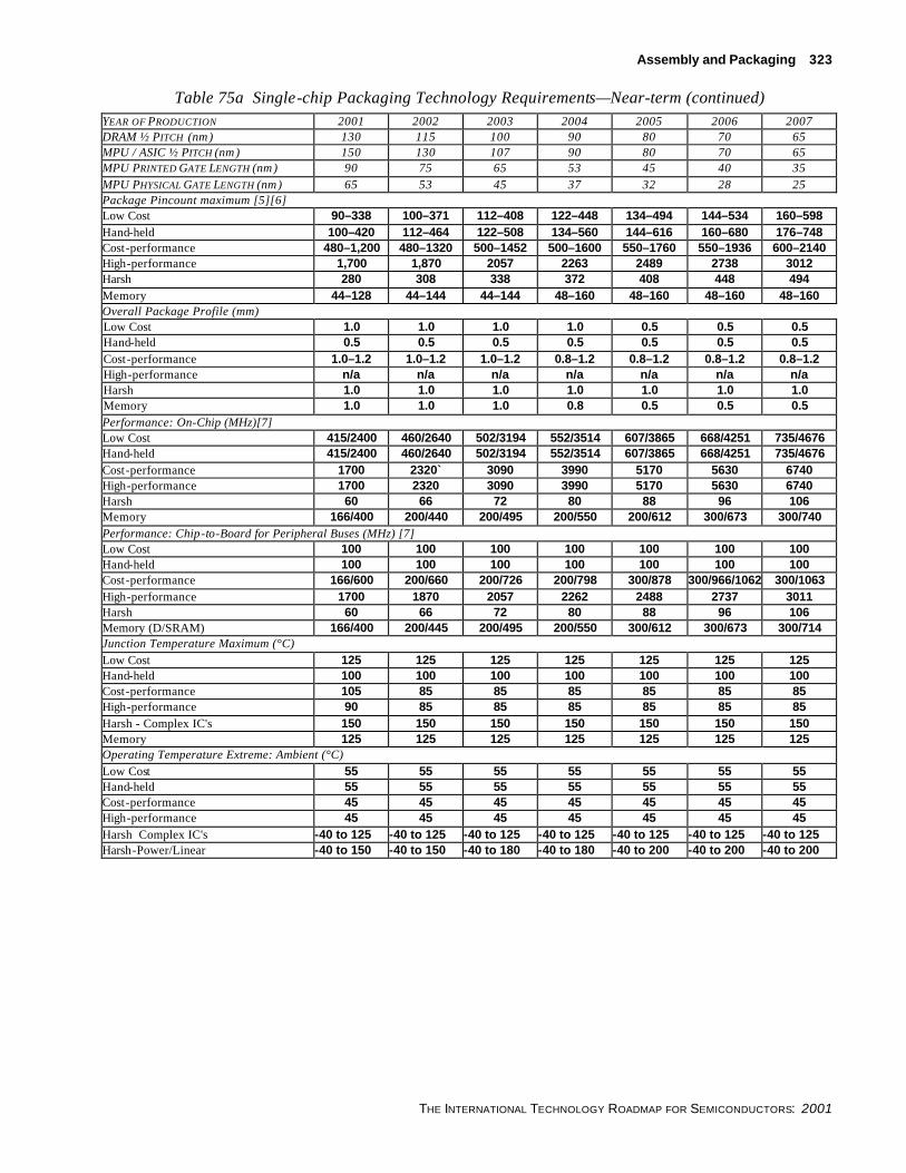
TECHNOLOGY REQUIREMENTS Packaging technology continues to change rapidly. Assembly and packaging needs are driven as much by market application requirements as by silicon technology. Cost will drive technology trade-offs for all market segments. The key single chip package technology requirements have been updated by the domestic and international TWGs as shown in Table 75a and b.
Although assembly and packaging costs are expected to decrease over time on a cost-per-pin basis, the chip and package pincount is increasing more rapidly than cost-per-pin is decreasing. This explosion in pin count is increasing not only the absolute cost of assembly and packaging on a per-chip basis, but also the substrate and system-level packaging costs. In low-cost and hand-held product catagories, the cost per pin cost decreases are also expected to flatten out over the next several years, which will drive a faster rate of package cost increase in these segments. To satisfy the requirements for the increasing numbers of pins needed to leverage silicon productivity more fully, the industry must implement affordable new assembly and packaging technologies that will be more independent of pincount.
Pin count will continue to increase in all segments but with the flattening of maximum chip size this will drive a need for reduction in I/O pitch. The off-chip digital frequency has increased to now match on-chip in some high-speed communications applications, which will drive the need for improved package signal integrity. The need for very high speed digital pins and high frequency RF I/O requirements have also been added to the requirement tables.
Packaging technology that addressees very high-power density has already been developed for high-end applications, but will need to be cost-reduced to enable broader applications.
Table 75a Single-chip Packaging Technology Requirements—Near-term YEAR OF PRODUCTION 2001 2002 2003 2004 2005 2006 2007 DRAM ½ PITCH (nm) 130 115 100 90 80 70 65 MPU / ASIC ½ PITCH (nm) 150 130 107 90 80 70 65 MPU PRINTED GATE LENGTH (nm) 90 75 65 53 45 40 35 MPU PHYSICAL GATE LENGTH (nm) 65 53 45 37 32 28 25 Cost (Cents/Pin) [1][2] Low Cost 0.30–0.75 0.28–0.68 0.26–0.62 0.25–0.56 0.24–0.51 0.23–0.46 0.22–0.41 Hand-held 0.45–0.90 0.42–0.81 0.40–0.73 0.38–0.65 0.36–0.60 0.34–0.56 0.32–0.52 Cost-performance 0.80–1.60 0.75–1.44 0.70–1.30 0.66–1.17 0.61–1.06 0.56–1.03 0.53–1.00 High-performance 2.20 2.09 1.98 1.88 1.78 1.69 1.61 Harsh 0.45–4.00 0.40–3.60 0.36–3.20 0.32–2.88 0.29–2.59 0.26–2.33 0.23–2.11 Memory 0.36–1.54 0.34–1.39 0.32–1.26 0.30–1.14 0.28–1.03 0.27–0.93 0.27–0.84
Chip Size (mm2) [3] Low Cost 57 59 61 63 65 65 65 Hand-held 57 59 61 63 65 65 65 Cost-performance 170 178 186 195 204 204 204 High-performance 310 310 310 310 310 310 310 Harsh 60 80 100 100 100 100 100 Memory 127 141 157 175 175 175 175 Power: Single Chip Package (Watts) [4] Low Cost n/a n/a n/a n/a n/a n/a n/a Hand-held 2.4 2.6 2.8 3.2 3.2 3.5 3.5 Cost-performance 61 75 81 85 92 98 104 High-performance 130 140 150 160 170 180 190 Harsh 14 14 14 16 16 18 18 Memory 1.2 1.4 1.6 1.8 2.0 2 2 Core Voltage (Volts) Low Cost 1.8 1.2 1.2 1.2 1.2 0.9 0.9 Hand-held 1.2 1.2 1.1–1.2 1.1–1.2 1.1–1.2 1.0–1.2 0.9–1.1 Cost-performance 1.8 1.5 1.5 1.2 1.2 0.9 0.9 High-performance 1.1 1.0 1.0 1.0 0.9 0.9 0.7 Harsh 3.3 2.5 2.5 2.5 1.2 1.2 1.2 Memory 1.8 1.5 1.5 1.2 1.2 1.2 0.9
Assembly and Packaging 323
THE INTERNATIONAL TECHNOLOGY ROADMAP FOR SEMICONDUCTORS: 2001
Table 75a Single-chip Packaging Technology Requirements—Near-term (continued) YEAR OF PRODUCTION 2001 2002 2003 2004 2005 2006 2007 DRAM ½ PITCH (nm) 130 115 100 90 80 70 65 MPU / ASIC ½ PITCH (nm) 150 130 107 90 80 70 65 MPU PRINTED GATE LENGTH (nm) 90 75 65 53 45 40 35 MPU PHYSICAL GATE LENGTH (nm) 65 53 45 37 32 28 25 Package Pincount maximum [5][6] Low Cost 90–338 100–371 112–408 122–448 134–494 144–534 160–598 Hand-held 100–420 112–464 122–508 134–560 144–616 160–680 176–748 Cost-performance 480–1,200 480–1320 500–1452 500–1600 550–1760 550–1936 600–2140 High-performance 1,700 1,870 2057 2263 2489 2738 3012 Harsh 280 308 338 372 408 448 494 Memory 44–128 44–144 44–144 48–160 48–160 48–160 48–160 Overall Package Profile (mm) Low Cost 1.0 1.0 1.0 1.0 0.5 0.5 0.5 Hand-held 0.5 0.5 0.5 0.5 0.5 0.5 0.5 Cost-performance 1.0–1.2 1.0–1.2 1.0–1.2 0.8–1.2 0.8–1.2 0.8–1.2 0.8–1.2 High-performance n/a n/a n/a n/a n/a n/a n/a Harsh 1.0 1.0 1.0 1.0 1.0 1.0 1.0 Memory 1.0 1.0 1.0 0.8 0.5 0.5 0.5 Performance: On-Chip (MHz)[7] Low Cost 415/2400 460/2640 502/3194 552/3514 607/3865 668/4251 735/4676 Hand-held 415/2400 460/2640 502/3194 552/3514 607/3865 668/4251 735/4676 Cost-performance 1700 2320` 3090 3990 5170 5630 6740 High-performance 1700 2320 3090 3990 5170 5630 6740 Harsh 60 66 72 80 88 96 106 Memory 166/400 200/440 200/495 200/550 200/612 300/673 300/740 Performance: Chip-to-Board for Peripheral Buses (MHz) [7] Low Cost 100 100 100 100 100 100 100 Hand-held 100 100 100 100 100 100 100 Cost-performance 166/600 200/660 200/726 200/798 300/878 300/966/1062 300/1063 High-performance 1700 1870 2057 2262 2488 2737 3011 Harsh 60 66 72 80 88 96 106 Memory (D/SRAM) 166/400 200/445 200/495 200/550 300/612 300/673 300/714 Junction Temperature Maximum (°C) Low Cost 125 125 125 125 125 125 125 Hand-held 100 100 100 100 100 100 100 Cost-performance 105 85 85 85 85 85 85 High-performance 90 85 85 85 85 85 85 Harsh - Complex IC's 150 150 150 150 150 150 150 Memory 125 125 125 125 125 125 125 Operating Temperature Extreme: Ambient (°C) Low Cost 55 55 55 55 55 55 55 Hand-held 55 55 55 55 55 55 55 Cost-performance 45 45 45 45 45 45 45 High-performance 45 45 45 45 45 45 45 Harsh Complex IC's -40 to 125 -40 to 125 -40 to 125 -40 to 125 -40 to 125 -40 to 125 -40 to 125 Harsh-Power/Linear -40 to 150 -40 to 150 -40 to 180 -40 to 180 -40 to 200 -40 to 200 -40 to 200

324 Assembly and Packaging
THE INTERNATIONAL TECHNOLOGY ROADMAP FOR SEMICONDUCTORS: 2001
Table 75b Single-chip Packaging Technology Requirements—Long-term YEAR OF PRODUCTION 2010 2013 2016 DRAM ½ PITCH (nm) 45 32 22
MPU / ASIC ½ PITCH (nm) 50 35 25 MPU PRINTED GATE LENGTH (nm) 25 18 13
MPU PHYSICAL GATE LENGTH (nm) 18 13 9
Cost (Cents/Pin)[1] [2] Low Cost 0.22–0.49 0.19–0.42 0.19–0.39
Hand-held 0.27–0.70 0.23–0.67 0.20–0.56 Cost-performance 0.49–0.98 0.42–0.93 0.36–0.79
High-performance 1.68 1.44 1.22
Harsh 0.27–1.54 0.23–1.12 0.20–.9 Memory 0.22–0.54 0.19–0.39 0.19–0.33
Chip Size (mm2)[3]
Low Cost 81 90 90 Hand-held 81 90 90
Cost-performance 268 307 307 High-performance 310 310 310
Harsh 150 150 150
Memory 191 250 250 Power: Single Chip Package (Watts)[4]
Low Cost N/A N/A N/A Hand-held 3 3 3
Cost-performance 119.6 137.6 158.2
High-performance 218 250.7 288.3 Harsh 20.7 23.8 27.4
Memory 2.3 2.65 3.05 Core Voltage (Volts)
Low Cost 0.6 0.5–0.6 0.3
Hand-held 0.5 0.4 0.4 Cost-performance 0.6 0.6 0.5
High-performance 0.6 0.5 0.4 Harsh 1.2 0.9 0.9
Memory 0.6 0.6 0.3 Package Pincount [5] [6] Low Cost 208–777 270–1011 351–1314
Hand-held 229–972 298–1264 387–1643 Cost-performance 780–2782 1014–3616 1318–4702
High-performance 4009 5335 7100 Harsh 642 835 1086
Memory 62–208 81–270 105–351
Overall Package Profile (mm) Low Cost 0.8 0.5 0.5
Hand-held 0.65 0.50 0.5 Cost-performance 0.65–0.80 0.50–0.65 0.5–0.65
High-performance n/a n/a n/a
Harsh 1.0 1.0 0.8 Memory 0.65 0.50 0.5

Assembly and Packaging 325
THE INTERNATIONAL TECHNOLOGY ROADMAP FOR SEMICONDUCTORS: 2001
Table 75b Single-chip Packaging Technology Requirements—Long-term (continued) YEAR OF PRODUCTION 2010 2013 2016 DRAM ½ PITCH (nm) 45 32 22
MPU / ASIC ½ PITCH (nm) 50 35 25 MPU PRINTED GATE LENGTH (nm) 25 18 13
MPU PHYSICAL GATE LENGTH (nm) 18 13 9
Performance: On-Chip (MHz) [7] Low Cost 956–6079 1243–7903 1616–10274
Hand-held 956–6079 1243–7903 1616–10274 Cost-performance 12000 19000 29000
High-performance 12000 19000 29000
Harsh 138 179 234 Memory 450/984 600/1280 750/1665
Performance: Chip-to-Board for Peripheral Buses (MHz)[7] Low Cost 125 125 150
Hand-held 125 125 150
Cost-performance 300/1415 300/1883 300/2506 High-performance 4009 5339 7100
Harsh 125 125 150 Memory (S/SRAM) 250/761 250/963 250/1175
Junction Temperature Maximum (°C) for Cost- performance
Low Cost 125 125 125 Hand-held 100 100 100
Cost-performance 85 85 85 High-performance 85 85 85
Harsh 150 150 150
Harsh-Complex IC's 190 190 190 Memory 100 100 100
Operating Temperature Extreme: Ambient (°C) Low Cost 55 55 55
Hand-held 55 55 55
Cost-performance 45 45 45 High-performance 45 45 45
Harsh -40 to 125 -40 to 125 -40 to 125 Harsh-Complex IC's -40 to 150 -40 to 150 -40 to 150
Memory 55 55 55
Notes for Tables 75a and b:
[1] Cost decreases will slow down on the lowest cost catagories as technology matures and economy of scale benefits are reduced.
[2] Cost refers to the average contract assembly cost per pin for each category.
[3] Die sizes for high performance will not increase beyond 310mm and cost performance die sizes will flatten out as die size approaches 310mm).
[4] Power will be limited more by system level cooling and test constraints than packaging.
[5] Pin counts will be limited for some applications by system level PWB cost impact.
[6] The pin counts assume the signal to reference pin ratios will vary from 1:4 to 2:1 across different markets segments.
[7] Maximum off-chip frequency will be limited to a small number of pins in many cases combined with a large number of lower frequency pins.
PACKAGE DESIGN REQUIREMENTS
Package design complexity (chip-to-module and chip/module-to-board) and scope are continuously increasing while the market intensifies the demand for design cycle time reduction and high design confidence. Physical, electrical, thermal, mechanical, assembly, and manufacturability considerations, in addition to cost and availability, confront the package designer. The package design process requires continuous improvements in design and analysis tools. The tools for layout, wiring, electrical, mechanical, and thermal design tasks must enhance usability and minimize interface incompatibilities if design cycle reductions are to be realized. The goal is an integrated design system. The scope of this integrated design system must include or be coordinated with chip design so that efficient chip/package co-design is feasible. Ideally, it should be linked to the system design so as to incorporate those requirements and trade-offs.

326 Assembly and Packaging
THE INTERNATIONAL TECHNOLOGY ROADMAP FOR SEMICONDUCTORS: 2001
THERMAL MANAGEMENT
The task of dissipating the heat from integrated circuits while maintaining acceptable junction temperatures has been a significant challenge for semiconductor and system manufacturers. Power, wattage, and junction temperature requirements are shown by market segment in Table 75a and b. These ITRS projections indicate that the thermal management challenge will significantly increase in the future due to increasing power, decreasing junction temperatures, and a continuing need to have cost-effective solutions.
In the hand-held market segment, power availability is limited by battery power. The power dissipation is currently limited by the user (the heat sink is the hand or lap), and cooling is usually accomplished without forced air. Challenges increase from the desire to use higher power devices with the increasing convergence of computing with communication (driving higher performance and power in this market); and with an increasing need for system level cooling (more than one hot device). Solutions could include use of higher thermal conductivity materials, reduction in internal thermal resistance, and potentially in more novel approaches to manage cooling while not discomforting the user. Cooling needs to be an integral part of the product design.
Desktop processors for the cost-performance market have required forced air cooling for the system, and have represented a wide spectrum of electronic products. With area array flip chip, the backside of the chip provides a direct heat path for cooling. The packaging challenge has been to create an interface with the chip that provides very low thermal resistance, is cost effective, reliable, and also enables system level solutions. System cooling design must also be acceptable in this market, with implications to cost, acoustic noise, reliability, and high volume manufacturing. As Table 75a and b shows, power is expected to continue to increase while target junction temperatures decrease. In 2002 this equates to a ∆T of 45° (and shrinking over time) with the ambient. At an expected power of 75 Watts (and growing over time), this becomes a significant challenge for acceptable solutions in the cost-performance market, and further highlights the need for complete, integrated, chip-to-system solutions. Some of the key developments and innovations are: more advanced/efficient air-cooling, boundary layer control, engineered surfaces, and cost-effective alternative cooling systems.
Notebook computing products are also in the cost-performance market segment. While they may not push the highest power levels while on battery operation, they do pose significant cooling requirements based on form factor, weight, and ergonomic issues (maintaining comfortable outer case temperatures for the user). Additional developmental areas would include redirection of internal thermal resistance, engineered surfaces, new novel cooling systems, and solutions that allow multiple and different power levels for the product.
The high-performance market sector has experienced a dramatic increase in power over the different generations. Air-cooling has been the preferred option to keep costs within bounds. In addition to managing total chip power requirements in excess of 100 Watts, solutions to manage power density and internal hot spots are necessary. Assuming identical junction and ambient temperatures, the higher power levels in this sector will demand a 40%–50% reduction in junction to ambient thermal resistance compared with the cost-performance segment. Current solutions are already focused on complete integration from the chip through the system, and this approach will need to continue. Significant engineering development will be needed for power increases at each technology generation, with capabilities needed equivalent to closed-loop cooled systems. Solutions must of course also be acceptable to the end-use customers. A major additional challenge will be to ensure that thermal management does not impede the migration path of products from this sector into the cost-performance market.
PACKAGING MATERIALS REQUIREMENTS
Dramatic improvements in materials properties—to address high frequency, higher power density, and increased mechanical stress—will be required to support 2005 through 2016 requirements. Major efforts have been underway to address environmental concerns such as for lead free solder assembly implementation and for halogen free materials, and they are expected to continue in the coming years. Significant new materials research and process development continues to be needed in a number of areas in the coming years. For example no materials solution is as yet known for drop in solder replacement for high temperature (high lead) applications including Pb based solder die attach. Additionally performance indicators like dielectric constant, dielectric loss, and thermal conductivity will be very significant to meet higher frequency and higher power demands. Materials research and development will be needed to meet thermal management challenges such as for thermal interface materials, heat spreaders, and external solutions. Knowledge of packaging materials properties are critically needed for modeling and simulation of electrical, thermal, and reliability performance for package design release and new package development. Methods for accurate characterization of materials properties and materials interface properties for packaging materials in their use environment will be needed.

Assembly and Packaging 327
THE INTERNATIONAL TECHNOLOGY ROADMAP FOR SEMICONDUCTORS: 2001
Establishment of materials data base to make the materials information available to the community will be very important.
RELIABILITY REQUIREMENTS
With the introduction of many new package formats, copper chip interconnect, low K chip dielectrics, direct chip attach, and area array interconnect there are many new requirements to packaged device reliability. Many of these new materials and package configurations require extensive characterization given the lack of historical reliability data. Extensive use of simulation to help validate and understand reliability performance is also required to assure these technologies are deployed with reasonable risk factors.
Some new package designs, materials, and technologies will not be capable of reliable performance in all market applications. More in-depth knowledge of the relevant failure mechanisms coupled with knowledge of the market use conditions will be required to bring new package technologies to the marketplace. Better definition of environmental requirements for each market segment would facilitate package development tailored to the market needs and help ensure consistent reliability performance among suppliers as well as between suppliers and customers. More research emphasis on physical and thermo -mechanical models of failure mechanisms is needed to support this trend.
Conception and development of tools for rapid electrical and physical fault isolation of package and interconnect technologies is critical. Faster techniques are needed to execute statistically significant studies of material bulk and interface properties. Developing extensions of current fault isolation and package analytical technologies (such as X-ray, acoustic, and Moire) needs to be balanced with development of new technologies for small defect visualization (such as X-ray tomography). Organic chemical interface analysis techniques are growing in importance with the introduction of new organic materials. Low alpha materials need to be considered during the timeframe of the ITRS to reduce errors induced by alpha radiation. Measurement techniques and standards for alpha radiation effects are not adequate to support the increased alpha sensitivity anticipated for advanced technology processes.
Interfacial delamination will continue to be a critical reliability hazard that is worsened by the trend to larger chips and new materials. Standard methods and acceptance criteria for interfacial adhesion are lacking. Fundamental work is needed to establish adhesion strength and degradation rate versus environmental factors (temperature, relative humidity) as well as a function of interfacial physical (such as roughness, composition) and chemical (van der Waals, dipole, covalent) properties. The CTE mismatch between the chip and the substrate should be reduced to mitigate large chip packaging-related reliability issues.
New electrostatic discharge (ESD) test methods and equipment are required to comprehend increasing pincount and shrinking interconnect pitch. Improved handling solutions for bare chip and packaged devices will help ESD related reliability issues.
MEMS REQUIREMENTS
MEMS technology has broadly expanded in the last decade to become the standard for many automotive, medical, telecommunications, and consumer electronics applications and the predicted market growth for MEMS technology is very high. One of the major bottlenecks for the continued growth of MEMS products has been packaging technology.
Like standard semiconductor devices, MEMS devices need environment protection, electrical signal integrity, mechanical support, and thermal management. However, in addition, MEMS may require packaging that provides access to chemical or biological environments they interact with. Many of the MEMS applications also demand inert/vacuum inside the package. For example: pressure sensors “media compatible” for the disposable blood pressure application are not “media compatible” for a 10-year automotive application. As a result, even though the functionality of two MEMS could be the same, the differences in environment drive quite different package requirements. To effectively reduce cost, improved manufacturability, and improve reliability standardized technologies need to be develop that can handle this broad range of requirements. MEMS do not require high pin counts, or very fine pad pitches for interconnect.
Some single chip ceramic, molded, chip scale, and wafer level packaging technologies have been used successfully to address some of these applications requirements. However, MEMS multichip packages and 3D packaging solutions are still under development.
To meet product performance requirements MEMS devices and packaging designers must consider the interface of structural elements, signal processing and power elements, signal and energy changing elements, material technology,

328 Assembly and Packaging
THE INTERNATIONAL TECHNOLOGY ROADMAP FOR SEMICONDUCTORS: 2001
harsh media compatibility, test equipment process and standards, packaging techniques and processes. While many of these issues are common with semiconductor packaging some are unique to MEMS. CADs systems package design standards and methodologies, packaging assembly attributes, reliability standards and assessment and interfaces of micro and macro packaging attributes need to be developed to handle these unique design requirements.
0PTOELECTRONICS REQUIREMENTS
Figure 52 Optoelectronics Package Design Illustration
Optoelectronics packaging brings together two realms of component packaging—the traditional electronic packaging with its associated issues (covered elsewhere in this chapter) and the integration of optical components into the module. Figure 52 is an illustration of an optoelectronic design. The electronic packaging issues may be viewed as a special case of mu lti-chip packaging. I/O counts are typically lower and die sizes are smaller than standard multi-chip modules. The main issue is the high data rates and low signal levels of the converted optical signal. Another challenge is integration of optical functionality into the module. Optical functionality includes passive devices such as array waveguide gratings (AWG), filters, splitters etc and active devices including lasers, modulators detectors and amplifiers switches and attenuators.
The key mechanical issues with optoelectronics packaging is aligning the optical path and maintaining this alignment under all service conditions. Typical systems for higher data rates utilize a 9.3 µm diameter fiber core that needs to be aligned to a narrow active device. For example, a detector for 10 Gbits use may have an active area on the order of 25 µm. The transmitter (laser) alignment tolerances are even more stringent with the mode size of the order of 10 µm and a mode shape that would need to be converted to match the fiber mode. This may require additional optics (lenses) between the laser diode and the fiber. Each added optic adds to the alignment complexity and increases the loss. These interfaces can be a large source of attenuation greatly impacting the system loss budget. Hermetic packaging is used to keep the optical pathway clear of contamination. Contamination in the pathway leads to additional loss and can damage the optical surfaces through absorption-generated heat or focusing of the optical beam. Cost reduction, especially for Metro applications, is driving the need to develop a non-hermetic approach. Fiber feed-throughs in the hermetic package add a great deal of complexity and cost. Care needs to be taken in mounting the optical components due to strain-induced birefringence. This effect can cause wavefront distortion and scattering.
The main issue in assembly is how to automate the alignment process to reduce costs. A standardized approach to packaging and alignment would ease the development of automation equipment. Currently, only a few high volume manufacturers are automating their processes. Simple issues such as how to handle fiber pigtails through an automation process need to be addressed as well as standardized carriers and systems.
A better understanding of the materials properties is necessary to successfully engineer optoelectronics packages. The optoelectronics package may contain substrates as diverse as silicon, AlGaAs, InP, Polymer, SiGe in various
Source Optical Component
Focusing LensCollimating Lens
Fibre
Optical Bench
Focusing Lens
Collimating Lens
Package
Assembly and Packaging 329
THE INTERNATIONAL TECHNOLOGY ROADMAP FOR SEMICONDUCTORS: 2001
combinations in one package. An understanding of the thermomechanical effects and material interactions will be necessary for the fabrication of reliable packages. Viscoelastic properties of the mounting adhesives will be necessary to understand the environmental stressing behavior of fiber alignment mountings.
Integrated design capabilities will need to be developed for optoelectronics packaging. Design systems that encompass the optical, electrical, thermal, and mechanical requirements of these packaged systems are needed.
Thermal Management requirements in optoelectronic packaging are more stringent than in their electronic counterparts. Whereas thermal management in standard electronics is primarily for reliability concerns, in optoelectronics many devices have a temperature sensitivity to their operating parameters, such as wavelength. Indeed, it is common to use temperature tuning of the optical devices in order to operate on a specific wavelength on the ITU grid. This leads to a need for integration of thermo -electric (Peltier) coolers into the package and an adequate method for dissipating the waste heat. Future devices will be densely packed and operate at very high rates (10 Gbits, 40 Gbits…. 160 Gbits), which will only further exacerbate the thermal issues. Additionally, thermal drift will impact fiber alignment through differential expansion of the different components of the package. The optoelectronic packages may include optical devices such as laser diodes, photo diodes, light guides, and fibers. Since the characteristics of many of these components are temperature sensitive, the efficient control of the operating temperatures of the packages is required.
Optoelectronics packaging materials comprised of conventional electronic packaging materials, light guiding materials, optical positioning adhesives, and white light producing phosphor coatings. The challenge arises out of the fact that apart from meeting the requirements for electronic devices, the needs such as thermal stability, refractive index and assembly tolerance of optical devices/materials must also be met during assembly. Light guiding materials should exhibit very low loss of optical signals, high thermal stability to allow reflow processing, low birefringence, easy control of refractive index, and ease of processing.
FLIP CHIP REQUIREMENTS
Wafer bumping is a key element to the successful implementation of flip chip technology as required by the ITRS. Eutectic Sn/Pb bumps on organic substrates represent the target against which potential solutions should be benchmarked. There are several challenges to implementation and proliferation including cost, density, manufacturability, availability, and compatibility with on-chip Cu/low κ materials. Potential solutions to reduce soft error upset from alpha particle emissions could include moving to low alpha Pb and Pb-free solders during the timeframe of this Roadmap. Cost for bumping a wafer (on a per-chip basis, including the under bump metallurgy and the bump deposition) needs to decrease continuously over the period through process simplification. Any lower cost process must preserve reliability, quality, and yield. Bump pitch will decrease from 160 µm or greater today, to 70 µm by the end of the period for high I/O and high-power chips. This will increase the wireability requirements for the substrate significantly. For low I/O chips in low-cost and hand-held applications, the bump pitch must be reduced continuously to address shrinking die sizes without degrading high frequency performance. Bumped wafers and chips must become generally available at a cost below packaged devices but at an equal quality level.
Test has the greatest technical challenge to achieve the quality goal. Test contactor reliability must be achieved at elevated temperatures without inducing bump damage. The flip chip must be, and be perceived to be, equivalent to a packaged device. Achieving this perceived equivalence is the greatest short-term challenge and needs greater industry focus for success.
EMBEDDED PASSIVES REQUIREMENTS
The needs for embedded passives on packages have been variously described to be (a) saving on package real estate, (b) improving performance through shortened path, and (c) saving in cost of component and assembly. The alternate is discrete passives on package or implementation on chip. Embedded passives will be implemented only when there are competitive advantages in either cost, performance, or functionality as compared to discrete passives or on-chip passives. With the cost and size of the discrete passives continue to decrease, the embedded passives will likely to find first implementations in specific areas where discrete or on-chip solutions are not suitable. While research in materials and manufacturing processes for embedded resistors, capacitors, and inductors are proceeding, there would be a need for integrated package design tools that would include embedded passives in the design processes.
Discrete resistors can achieve the tight tolerance by sorting, and have extremely low cost and small size. Embedded resistors are used not because of size or materials cost benefit. Instead, a designer may use embedded resistors when discrete resistors are not sufficient to meet the performance need due to its parasitic inductance and capacitance. The most important issue for embedded resistor is their tolerance in the performance-oriented applications.

330 Assembly and Packaging
THE INTERNATIONAL TECHNOLOGY ROADMAP FOR SEMICONDUCTORS: 2001
The printed wiring board could use a large number of terminating resistors. The savings from the piece parts and their assembly cost of a large number of discrete resistors may be sufficient to trade-off the additional cost associated with the embedded resistor layer and the required laser trimming. However, the materials resistance range, stability of sheet resistivity in long-term usage, and the temperature coefficient of resistivity still need improvement, particularly when used in package substrate applications.
The optoelectronic applications are pushing for broadband applications. These applications need high precision resistors as close to the ICs as possible. Customers are willing to pay for the additional cost of laser trimming on embedded resistors on the packages.
For those applications, where 15% tolerance is sufficient, on-chip resistors will be used. Resistors must also have very high density to meet the high I/O leadcount requirements. There is no benefit to use the embedded resistors on the package, unless the high precision is achieved using laser trimming. The density constraint will limit it to medium I/O applications. The broadband opto-electronic module manufacturers often depend on the third party library services offered by the semiconductor foundries for I/O interface circuits, which may not include the required on-chip terminating resistors.
At the present time, the chipset users encounter the need to get different ICs from different sources. The terminating resistors may or may not be on the chipset ICs. The graphic DRAM ICs connected to the chipset ICs may or may not have the terminating resistors. There is a desire to have embedded terminating resistors on the packages. Such package may be used in the point-to-point wiring nets. For multi-drop wiring net, a terminating resistor is need at the end of a long transmission line. It is usually placed on the PWB, not on the packages. In other words, it is desirable to have embedded resistors on the package for the point-to-point wiring net.
However, the additional cost should be very little, because the IC cost will remain the same when the terminating resistors are eventually integrated on the IC. Furthermore, the on-chip terminating resistors are more flexible. They may be connected or disconnected under IC control. That is, they may be used for point-to-point as well as the multi-drop wiring nets.
If implementation of embedded resistors requires an additional layer on the package substrate, the additional layer cost would have to be amortized over the cost of all the resistor components. However, if they can be implemented over unused real estate on the package and require little additional process steps in substrate processing, the economic justification will be more compelling.
For RF applications, resistors in the range of 20 to 100 Ohm are used for load and termination. Discrete resistors may be sorted to get the precision required. Embedded resistors will need trimming to get the required precision. Those in the range of 100 Ohm to 250K Ohm are used for biasing and circuit stability purpose. The cost of a chip resistor and its assembly on PWB is about one cent or less per resistor. This is the cost target for the trimmable, embedded on-package resistors.
De-coupling capacitors are needed as reservoirs of electrical charges to minimize switching noise in the electronic system. The rise/fall switching transition is very short in the IC, has a medium duration in the package, and is longest on the printed wiring board. Therefore, designers want high-frequency de-coupling capacitors on the IC, or very close to it to minimize the series inductance and resistance; mid-frequency de-coupling capacitors on the package; and low-frequency/high-capacitance de-coupling capacitors on the PWB.
For RF applications, capacitors in the range of 1 to 100 pF with 10% tolerance are used for RF tuning circuits. Those in the range of 10 to 1000 pF with 10 to 15% tolerance are used for IF tuning circuits. Those in the range of 100 pF to 100 nF with 15 to 25% tolerance are used RF bypass applications. The embedded capacitors may achieve the 15% tolerance, and may be used for IF tuning, DC blocking, and RF bypass.
The discrete capacitors may be sorted to meet the required precision. The cost of a chip capacitor and its assembly on the PWB is about one to two cents per capacitor. The challenges are the minimization of the series resistance and inductance of the lead wires. The on-chip capacitor array may have a total value of 100 pF per array. They may be personalized through on-chip logic circuits to meet the value for the specific circuit requirement, which is not possible with on-package capacitors.
There are a few parameters affecting the quality value (Q) of a on-chip inductor, as follows:
• The semiconductor substrate is not an insulating material. The distributed capacitance between the inductor coil and the non-insulating substrate reduces the effective inductance.
• The high series resistance of the fine metal lines on IC.

Assembly and Packaging 331
THE INTERNATIONAL TECHNOLOGY ROADMAP FOR SEMICONDUCTORS: 2001
• The on-chip inductors have been used by RF circuit designers. For examples: impedance matching, filtering, and the LC-tank circuit in the oscillators. Oscillators without inductors have also been implemented.
The clock generation in the microprocessor IC may use one or more on-chip phase-lock-loops (PLL). Some PLLs may use LC-tank circuit in the oscillators. The highest frequency PLL may use the on-chip inductor. The additional on-chip PLLs may use on-package, either discrete or embedded, inductors in the tank circuits. Of course, there are PLLs free of any inductor element. The on-chip analog power supply to the on-chip PLLs may use on-chip series regulator, which uses on-chip de-coupling capacitors to remove noise from the digital sections.
The on-package inductor minimizes both constraints encountered by the on-chip inductors. The designers need to follow a few rules in laying out the desired inductors. They also have to pay close attention on magnetic flux linkage among adjacent inductors, which cause coupled noise. Note that the inductive coupling reaches a much farther distance than the capacitive coupling does. The designers have to be very careful about coupled noise concern when pushing for a high number of inductors on the package. The use of high permeability material will increase the inductance value.
There are several functions, which are implemented by passive components, and are too large to be integrated on the ICs. Some examples are antennas, baluns, filters, resonators, and RF shields. These structures required improved dimensional control in substrates and low-loss dielectrics in low-cost substrates.
RF AND MIXED-SIGNAL REQUIREMENTS
The packaging challenges in the RF and mixed-signal realm will become increasingly important as low-cost mobile and high bandwidth products expand across all market segments. The increasing performance of silicon SiGe, and GaAs devices coupled with dramatic device cost reductions have establish the need for very low-cost, high-performance packaging. The primary approach to date has been to focus on extending performance of establish low-cost wirebond packages through careful design optimization. However this approach will not support continued cost reductions and performance improvements on the long term. In the RF product area frequency will shift up to the 5 GHz range that will require improved dielectric loss, tighter control of parasitic variability due to process variations, and more precise electrical simulation capability. Flip chip attachment to package and embedded passives on the package will be key enabling technologies to package level performance. Low inductance and high-density packages like FBGA/CSP will enable designers to use lower cost partitioning solutions than the traditional ceramic modules.
Integrated modeling and simulation tools are required to drive down design cycle time to acceptable levels. Performance, physical size, and cost driven integration will continue to arrive at a single chip radio that combines memory, processor and mixed-signal functions, as discussed above. Fast design cycle time and accurate simulation at both the chip and package levels are enablers of this integration. High-speed test and higher level of functional test at the package level also become development challenges. Microelectromechanical systems (MEMS) will be used in the fabrication of filter, switch, oscillator and other components in the next two to four years. They offer the benefit of small size, low insertion loss, low power consumption, integration with ICs, and the potential of low cost with batch fabrication. Reliability, potential temperature sensitivity, and hermetic/vacuum packaging of MEMS devices are key development challenges. POTENTIAL SOLUTIONS WAFER LEVEL PACKAGING
The wafer level packaging process (WLP) is a technology in which all of the IC packaging is performed at the wafer level. A WLP technology can, for the first time, maintain the cost of the IC packaging as a constant percentage of the total wafer cost. This is possible because WLP reduces the cost of packaging the individual chips. A WLP technology requires that when the chip size shrinks in later years, all of the package interconnects will continuously be located within the chip outline (it must be a fan-in design, known as the real chip size package). From a systems perspective, the limitation on WLP is how many I/O can be placed under the chip and still have a board design that can be routed.
The primary application market for WLP technology is projected to be low to moderate I/O density applications, as typified by high yield DRAM, Flash, Analog, EEPROM, RF and other ICs with ≤ 100 total I/O and adequate silicon area.
FBGA packages from WLP technology reached the level of practical use in 2000. Its use will expand in the field of portable devices and other small-size devices that require high-density mounting. A key enabling technology to take full advantage of a WLP will be the development of wafer level test and burn-in. Most WLPs with I/O pitch equal to or greater than 0.5 mm do not require the use of underfill and can therefore be directly implemented into a standard surface mount technology (SMT) process flow.

332 Assembly and Packaging
THE INTERNATIONAL TECHNOLOGY ROADMAP FOR SEMICONDUCTORS: 2001
The comparison between Bare Chip mounting technique and WLP technology is indicated in Table 76. WLP technology can solve or eliminate the problems and restrictions involved in bare chip mounting, therefore packages from WLP will be an alternative to bare chip EEPROM.
Table 76 Comparison between Bare Chip Mounting and WLP Technology
Item Bare Chip Mounting Wafer Level Packaging Package Type — Real chip size package (FBGA)
Device Body Size Same as chip size Same as chip size
Terminal Design of Device All terminal pads shall be located in adaptable pitch on chip
All terminal pads shall be located in adaptable pitch on chip
Quality Assurance of Device Difficult (especially burn in test) Easy
Interconnection of Board Wire bonding (WB)
Flip chip bonding (FCB)
Solder ball terminal
Interconnecting Wire Length FCB can achieve the shortest connection length May be slightly longer than FCB for re-wire die and ball
Mounting Area on Board Slight larger than chip area (fan-out for WB)
(Under fill print area for FCB)
Same area as chip size
Reliability after Board Mounting Encapsulation and under-fill material required Near equal to conventional packages
Mountability on Board
Facility for bare chip assembly required
Difficult to repair
Multiple parts reflow available
Easy to be repaired by standard
SMT assembly process
CHIP-TO-NEXT-LEVEL INTERCONNECT
Table 77 illustrates the chip-to-next -level interconnect potential solutions. The values for wire bond in this table are for inline pad pitches, although a staggered bond pad configuration could achieve an effective pitch denser than the value shown. The flip chip connection requires fan-out wiring on the package. Signal leads are usually placed on the outer several rows together with many of the voltage and ground leads for easy fan-out and minimum package inductance. The inner regions of the area array may be used for voltage and ground connection to minimize the on-chip resistive voltage drop across the IC chip. The area array pad pitch is 160 µm now, and reduces to 130 µm for the 80 nm technology generation and beyond for cost-performance and high-performance market segments, where the signal I/O and chip power are very high. The infrequent change of the pad pitch is adopted to minimize the cost of the test probe head. This results in many long fan-out wires. Excessive crosstalk noise between parallel signal wires should be carefully assessed at the design stage. For some of the hand-held applications where the size and power of the chip are small, one may need area array pad pitch much smaller than that used for the cost-performance and high-performance market segments. This is shown in a separate row in Table 77. For the applications with low supply current, the anisotropic conductive adhesives may be used for the area array connections.

Assembly and Packaging 333
THE INTERNATIONAL TECHNOLOGY ROADMAP FOR SEMICONDUCTORS: 2001
Table 77 Chip to Next Level Potential Solutions YEAR OF PRODUCTION 2001 2002 2003 2004 2005 2006 2007 2010 2013 2016 DRAM ½ PITCH (nm) 130 115 100 90 80 70 65 45 32 22 MPU / ASIC ½ PITCH (nm) 150 130 107 90 80 70 65 50 35 25 MPU PRINTED GATE LENGTH (nm) 90 75 65 53 45 40 35 25 18 13 MPU PHYSICAL GATE LENGTH (nm) 65 53 45 37 32 28 25 18 13 9 Chip Interconnect Pitch (µm) Wire bond—ball 45 35 30 25 20 20 20 20 20 20 Wire bond—wedge 40 35 30 25 20 20 20 20 20 20 TAB* 40 40 40 40 30 30 30 30 30 30 Flip chip (area array for cost -performance and high-performance)
160 160 150 150 130 130 120 90 80 70
Peripheral flip chip for hand-held, low-cost, and harsh
150 130 120 110 100 90 80 60 45 30
To satisfy the high pincount and performance requirements in Table 77 flip chip will become the predominant technology for chip-to-next level interconnect. Wire bond technology will continue to evolve and will be the dominant interconnect for low-cost products until flip chip costs become favorable. The use of flip chip for low I/O, but high-frequency, RF packaging was discussed in a previous section. Size, weight, and performance driven products will need flip chip interconnect with area array I/O at a pitch of 160 µm or less. This interconnect approach will require compatible underfill and substrate technologies to be available at the necessary performance and cost. A level of interconnect can be eliminated with this technology. Material, process development, and metrology technology improvements will also be required to support flip chip implementation. Flip chip interconnect technology at area array pitches ≤ 150 µm will put extreme pressure on substrate density for I/O escape beneath the chip site.
BALL GRID ARRAY PACKAGES
For many applications in the 200+ pincount range, BGA packages will provide potential solutions. Many BGAs will utilize a wire bond interconnect on the periphery of the ICs. Area array flip chip connections to BGAs will be needed for high I/O or high power chips. Laminate based ball grid arrays will require the use of underfills to reduce the shear stress load on the flip chip interconnections for large die, due to the large difference in the CTE between the silicon IC and the substrate. The bending of the encapsulated flip chip on BGAs may become excessive for large chip sizes and could impact the thermal cooling path. The space transformation between the tight pad pitch on the IC chip and the relatively large pitch between the plated through hole (PTH) on the substrate is totally contained in the BGA package. The area array solder balls beneath the BGA package have the same pitch as that of the PTH or PTH pad on the substrate. To minimize the number of signal layers on the wiring board, the signal leads underneath the BGA can be confined to the outer several rows. The inner rows are taken by the IC chip and wire bond interconnections for the cavity-down BGA. For the cavity-up BGA, the inner rows are either not used or are restricted for voltage and ground connections. Table 78 shows the maximum possible pincount for potential BGA package solutions with respect to the solder ball array pitch.

334 Assembly and Packaging
THE INTERNATIONAL TECHNOLOGY ROADMAP FOR SEMICONDUCTORS: 2001
Table 78 Ball Grid Array Packages Potential Solutions
YEAR OF PRODUCTION 2001 2002 2003 2004 2005 2006 2007 2010 2013 2016
DRAM ½ PITCH (nm) 130 115 100 90 80 70 65 45 32 22
MPU / ASIC ½ PITCH (nm) 150 130 107 90 80 70 65 50 35 25
MPU PRINTED GATE LENGTH (nm) 90 75 65 53 45 40 35 25 18 13
MPU PHYSICAL GATE LENGTH (nm) 65 53 45 37 32 28 25 18 13 9
BGA Solder Ball Pitch (mm)
Low cost 1.00 1.00 0.80 0.80 0.65 0.65 0.65 0.50 0.50 0.5
Hand-Held 1.00 1.00 0.80 0.80 0.65 0.65 0.65 0.50 0.50 0.5
Cost-performance 1.00 1.00 0.80 0.80 0.65 0.65 0.65 0.50 0.50 0.5
High-Performance 0.80 0.80 0.80 0.80 0.65 0.65 0.65 0.50 0.50 0.5
Harsh 1.27 1.27 1.00 1.00 1.00 0.8 0.65 0.50 0.50 0.5
BGA Body Size (mm) and Possible Pincount
Low cost 20 | 361 21 | 400 18 | 484 18 | 484 16 | 576 16 | 576 17 | 625 15 | 841 17 | 1089 19 | 1369
Hand-Held 23 | 484 23 | 484 19 | 529 20 | 576 17 | 625 18 | 729 19 | 784 17 | 1089 19 | 1369 21 | 1681
Cost-performance 37.5 | 1396 37.5 | 1369 33 | 1600 33 | 1600 29 | 1936 29 | 1936 31 | 2209 27 | 2809 31 | 3721 35 | 4761
High-Performance 35 | 1849 37.5 | 2116 37.5 | 2116 40 | 2401 33 | 2500 35 | 2809 37.5 | 3249 33 | 4225 37.5 | 5476 45 | 7921
Harsh 17 | 169 17 | 169 14 | 169 15 | 196 15 | 196 13 | 225 11 | 256 14 | 729 15 | 841 17 | 1089 Body sizes rounded to nearest JEDEC size
FINE PITCH BGA /CHIP SCALE PACKAGES
Fine pitch BGA/chip scale packages (FBGA/CSP) provide a potential solution where low weight and small size are requirements. These packages are only slightly larger than the chip itself, and are available in a variety of configurations and materials combinations. The size may range from 4 to 21 mm. The 21 mm FBGA/CSP is for the high lead count applications. Table 79 shows examples of the maximum possible pincount for depopulated area array FBGA/CSP solutions with respect to the 10 and 21 mm package sizes, array I/O pitch, and number of rows. For these packages the solder ball pitch is a fraction of the PTH on the printed wiring board (PWB). Fan-out wiring connections are required on the PWB to reach the PTH. To minimize the fan-out requirements, only a few of the outer rows of the area array connections are used. FBGA/CSPs at 0.5 mm pitch will put pressure on the PWB interconnect density for I/O escape to reach the inter-level vias or the PTH in the PWB. When the number of rows accessed is four or higher, a build-up layer on the PWB will be needed.
These packages provide potential advantages of higher performance, higher density, and chip shrink transparency. For applications where FBGA/CSPs are redesigned to the minimum size possible each time the chip size is reduced, this redesign will drive a corresponding redesign of the PWB onto which the packages are assembled.
Table 79 Single Chip Packages Potential Solutions
YEAR O F PRODUCTION 2001 2002 2003 2004 2005 2006 2007 2010 2013 2016
DRAM ½ PITCH (nm) 130 115 100 90 80 70 65 45 32 22
MPU / ASIC ½ PITCH (nm) 150 130 107 90 80 70 65 50 35 25
MPU PRINTED GATE LENGTH (nm) 90 75 65 53 45 40 35 25 18 13
MPU PHYSICAL GATE LENGTH (nm) 65 53 45 37 32 28 25 18 13 9
FBGA/CSP area array pitch (mm) 0.40 0.40 0.40 0.40 0.30 0.30 0.30 0.30 0.30 0.30
FBGA/CSP size (mm/side) 10.00 10.00 10.00 10.00 10.00 10.00 10.00 10.00 10.00 10.00
#Rows / #Leads (one fan-out layer) 3/252 3/252 3/252 3/252 3/348 3/348 3/348 3/348 3/348 3/348
#Rows / #Leads (two fan-out layers) 4/320 4/320 4/320 4/320 5/540 5/540 5/540 5/540 5/540 5/540
FBGA /CSP size (mm/side) 21.00 21.00 21.00 21.00 21.00 21.00 21.00 21.00 21.00 21.00
#Rows / #Leads (one fan-out layer) 3/576 3/576 3/576 3/576 3/792 3/792 3/792 3/792 3/792 3/792
#Rows / #Leads (two fan-out layers) 4/572 4/572 4/572 4/572 5/1280 5/1280 5/1280 5/1280 5/1280 5/1280
A=integer (CSP size/pitch-1); R=# rows, # leads = (A-R)xRx4
Note: The fine pitch BGA and CSP packages will be limited to 500 I/O for many applications where system board level cost is a constraint
Assembly and Packaging 335
THE INTERNATIONAL TECHNOLOGY ROADMAP FOR SEMICONDUCTORS: 2001
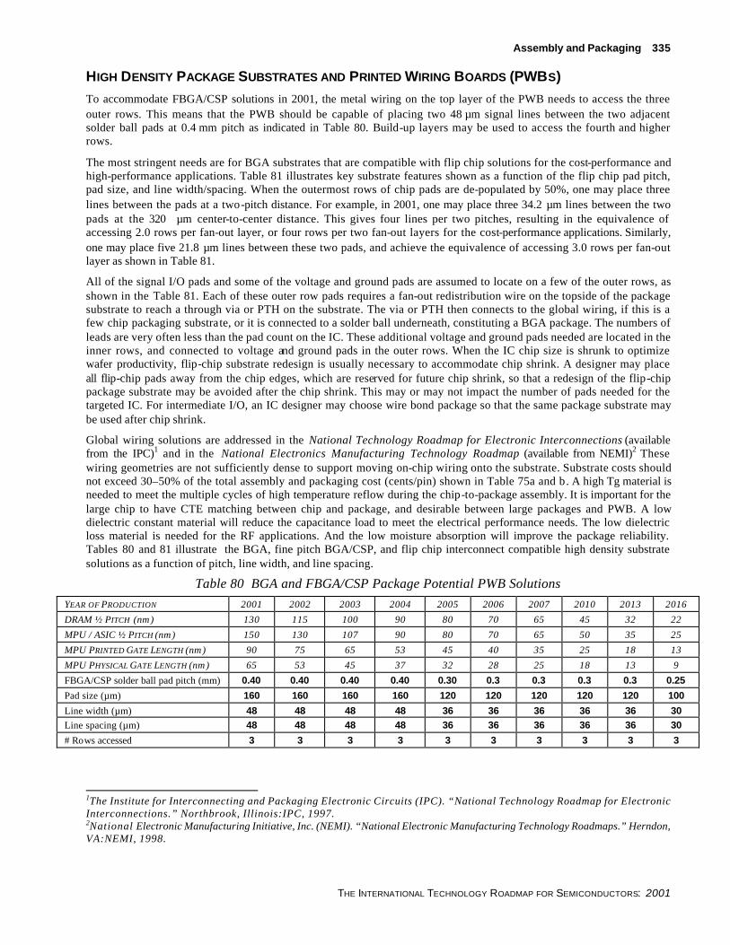
HIGH DENSITY PACKAGE SUBSTRATES AND PRINTED WIRING BOARDS (PWBS)
To accommodate FBGA/CSP solutions in 2001, the metal wiring on the top layer of the PWB needs to access the three outer rows. This means that the PWB should be capable of placing two 48 µm signal lines between the two adjacent solder ball pads at 0.4 mm pitch as indicated in Table 80. Build-up layers may be used to access the fourth and higher rows.
The most stringent needs are for BGA substrates that are compatible with flip chip solutions for the cost-performance and high-performance applications. Table 81 illustrates key substrate features shown as a function of the flip chip pad pitch, pad size, and line width/spacing. When the outermost rows of chip pads are de-populated by 50%, one may place three lines between the pads at a two-pitch distance. For example, in 2001, one may place three 34.2 µm lines between the two pads at the 320 µm center-to-center distance. This gives four lines per two pitches, resulting in the equivalence of accessing 2.0 rows per fan-out layer, or four rows per two fan-out layers for the cost-performance applications. Similarly, one may place five 21.8 µm lines between these two pads, and achieve the equivalence of accessing 3.0 rows per fan-out layer as shown in Table 81.
All of the signal I/O pads and some of the voltage and ground pads are assumed to locate on a few of the outer rows, as shown in the Table 81. Each of these outer row pads requires a fan-out redistribution wire on the topside of the package substrate to reach a through via or PTH on the substrate. The via or PTH then connects to the global wiring, if this is a few chip packaging substrate, or it is connected to a solder ball underneath, constituting a BGA package. The numbers of leads are very often less than the pad count on the IC. These additional voltage and ground pads needed are located in the inner rows, and connected to voltage and ground pads in the outer rows. When the IC chip size is shrunk to optimize wafer productivity, flip-chip substrate redesign is usually necessary to accommodate chip shrink. A designer may place all flip-chip pads away from the chip edges, which are reserved for future chip shrink, so that a redesign of the flip-chip package substrate may be avoided after the chip shrink. This may or may not impact the number of pads needed for the targeted IC. For intermediate I/O, an IC designer may choose wire bond package so that the same package substrate may be used after chip shrink.
Global wiring solutions are addressed in the National Technology Roadmap for Electronic Interconnections (available from the IPC)1 and in the National Electronics Manufacturing Technology Roadmap (available from NEMI)2 These wiring geometries are not sufficiently dense to support moving on-chip wiring onto the substrate. Substrate costs should not exceed 30–50% of the total assembly and packaging cost (cents/pin) shown in Table 75a and b. A high Tg material is needed to meet the multiple cycles of high temperature reflow during the chip-to-package assembly. It is important for the large chip to have CTE matching between chip and package, and desirable between large packages and PWB. A low dielectric constant material will reduce the capacitance load to meet the electrical performance needs. The low dielectric loss material is needed for the RF applications. And the low moisture absorption will improve the package reliability. Tables 80 and 81 illustrate the BGA, fine pitch BGA/CSP, and flip chip interconnect compatible high density substrate solutions as a function of pitch, line width, and line spacing.
Table 80 BGA and FBGA/CSP Package Potential PWB Solutions
YEAR OF PRODUCTION 2001 2002 2003 2004 2005 2006 2007 2010 2013 2016
DRAM ½ PITCH (nm) 130 115 100 90 80 70 65 45 32 22
MPU / ASIC ½ PITCH (nm) 150 130 107 90 80 70 65 50 35 25
MPU PRINTED GATE LENGTH (nm) 90 75 65 53 45 40 35 25 18 13
MPU PHYSICAL GATE LENGTH (nm) 65 53 45 37 32 28 25 18 13 9
FBGA/CSP solder ball pad pitch (mm) 0.40 0.40 0.40 0.40 0.30 0.3 0.3 0.3 0.3 0.25
Pad size (µm) 160 160 160 160 120 120 120 120 120 100
Line width (µm) 48 48 48 48 36 36 36 36 36 30
Line spacing (µm) 48 48 48 48 36 36 36 36 36 30
# Rows accessed 3 3 3 3 3 3 3 3 3 3
1The Institute for Interconnecting and Packaging Electronic Circuits (IPC). “National Technology Roadmap for Electronic Interconnections.” Northbrook, Illinois:IPC, 1997. 2National Electronic Manufacturing Initiative, Inc. (NEMI). “National Electronic Manufacturing Technology Roadmaps.” Herndon, VA:NEMI, 1998.

336 Assembly and Packaging
THE INTERNATIONAL TECHNOLOGY ROADMAP FOR SEMICONDUCTORS: 2001
Table 81 Flip Chip Substrate Top-side Fan-out Potential Solutions YEAR OF PRODUCTION 2001 2002 2003 2004 2005 2006 2007 2010 2013 2016
DRAM ½ PITCH (nm) 130 115 100 90 80 70 65 45 32 22
MPU / ASIC ½ PITCH (nm) 150 130 107 90 80 70 65 50 35 25
MPU PRINTED GATE LENGTH (nm) 90 75 65 53 45 40 35 25 18 13
MPU PHYSICAL GATE LENGTH (nm) 65 53 45 37 32 28 25 18 13 9 Flip Chip Pad Pitch (µm) 160 160 150 150 130 130 120 90 80 70 Pad Size (µm)* 80 80 75 75 65 65 60 45 40 35 Chip Size (mm/size)
Cost-Performance 12 12 12 12 12 12 12 12 12 12 High-Performance 17 17 17 17 17 17 17 17 17 17
Array Size = # pads along chip edge Cost-Performance (max) 74 74 79 79 91 91 91 132 149 170 High-Performance (max) 105 105 112 112 129 129 140 187 211 241
Wiring Substrate (Three lines replacing one depopulated pad-accessing 2.0 rows per fan-out layer) Line Width (µm) 34.2 34.2 32.1 32.1 27.8 27.8 25.7 19.2 17.1 15.0 Line Spacing (µm) 34.3 34.3 32.1 32.1 27.9 27.9 25.7 19.3 17.1 15.0
Wiring Substrate (Five lines replacing one depopulated pad-accessing 3.0 rows per fan-out layer) Line Width (µm) 21.8 21.8 20.4 20.4 17.7 17.7 16.3 12.2 10.9 9.5 Line Spacing (µm) 21.8 21.8 20.5 20.5 17.7 17.7 16.4 12.3 10.9 9.5
Wiring Substrate (Three lines between adjacent pads-accessing 4.0 rows per fan-out layer) Line Width (µm) 11.4 11.4 10.7 10.7 9.2 9.2 8.5 6.4 5.7 5.0 Line Spacing (µm) 11.4 11.4 10.7 10.7 9.3 9.3 8.6 6.4 5.7 5.0
* The pad size is assumed as 50% of pad pitch. It is usually different at different fan-out layers, e.g. from 30% to 60%
MULTI-CHIP PACKAGES / MULTI-CHIP MODULES / SYSTEM IN A PACKAGE
The 2000 input to this section did not address the major differences between the new wave of multichip package solutions and the previous obstacles and limitations associated with the MCM technologies—where adoption was limited primarily to lower volume high reliability applications. Beginning in 2000 driven by mobile phone applications, a shift is occurring in multichip packaging where the System in a Package (SiP) is becoming the fastest growing area of packaging due to its associated system integration benefits. SiP enables OEMs to maintain their size / weight reduction trends while integrating more features and functions through system package integration. This integration challenge may be best realized through cooperation between OEMs, their semiconductor device suppliers and microelectronic manufacturing service suppliers. The OEMs in these mobile phone applications have shorter product life cycles and have come to the realization that the designing new products is easier and more cost effective when you do not have to reinvent each detail from scratch.
The new definition of SiP could be as simple as just adding passive components to a single chip package to having multi-chips and or stacked chips in a single package with all the passive components included to provide a subsystem functional block. The SiP can be manufactured using ceramic, leadframe, organic laminate, or even tape-based substrates. The passive components can be either embedded as part of the substrate construction or soldered or epoxy attached on the substrate surface.
Die interconnect can be accomplished by either wire bonding, flip chip (soldered or epoxy), and/or TAB to the SiP substrate or die-to-die. The final package configuration can take the shape of a conventional ceramic style package, ball grid arrays, land grid arrays, and leadframe-based packages or custom modules. The resulting SiP utilizes die-to-die interconnection and high density substrate technologies to handle the higher wiring density requirements at the package level, thereby reducing the cost, wiring, and I/O densities required at the mother board and system level
Since SiPs were first adopted in high-volume, hand-held and wireless applications, their resulting low-cost infrastructure through the utilization of proven packaging platform technologies in high volume manufacturing lines enables new SiP configurations to be customized for a broad range of new applications. Any application that utilizes chip sets, embedded, or large memory blocks with high interconnect density requirements should evaluate SiP for their cost / performance optimization needs.

Assembly and Packaging 337
THE INTERNATIONAL TECHNOLOGY ROADMAP FOR SEMICONDUCTORS: 2001
The SiP packaging concept is here to stay for the following reasons and can be considered as the fourth wave of packaging innovation:
• Different die technologies such as GaAs, SiGe, or Si and Die functions such as logic, memory, RF, analog or digital can be assembled in the same package to achieve specific thermal, electrical and mechanical performance requirements.
• Dissimilar die geometries can be integrated from sub-micron of 0.10–0.13 µm in the same package cost effectively. The latest die technology can be used for each die function, therefore reducing cost and increasing performance.
• Other technologies such as MEMS , optical, or vision components may be included in the same SiP.
• Different interconnection technologies can be used—wire bond, flip-chip, or TAB—to connect to the package as well as each other.
• Other than passive components, antennas, baluns, filters, heat shrinks, resonators, connectors, and shields can be included in the same package.
• Revisions or upgrades to OEMs products are easily accomplished by using the latest die functions, therefore reducing the cycle time for those changes.
As the ability of the semiconductor sector increases to build true Systems on a Chip (SoC) not all the different components that need to complete a system can be cost effectively integrated on silicon. The SiP would then take on the responsibility to package the other non-silicon components into the package with the SoC device. The SiP will continue to become more complex and cost effective as new applications emerge. The final factor in favor of the SiP is the short cycle time it takes to create a new SiP or a modification of a present design. From design, characterization to manufacturing could be as short as 3–4 months while a SoC would take much longer. This cycle time reduction is why the SiP will continue to play a critical role in component packaging and system integration.
The SiP category does require new metrics for measuring cost-effectiveness. The cost-per-pin paradigm does not apply well to SiP and multichip package applications since the SiP greatly reduces the number of second-level connections through die-to-die interconnection within the package. Also the area and wiring density reductions associate with SiP provide system and motherboard cost reductions while enhancing reliability and performance. Both cost per area and total cost of ownership perspectives are required to fully appreciate the system integration cost and performance benefits delivered by SiP solutions. For instance, silicon efficiency is a new metric to measure the area effectiveness of bare die (wafer level packaging) versus multichip and 3D packaging solutions. Bare die or WLP achieve 100 % Si efficiency (where the die size and package sizes are equal) whereas emerging 3D (stacked die) packages are delivering over 200% Si efficiency using the previous measurement methods.
The SiP infrastructure faces the following challenges as it continues to grow
• Design tools for the package
• Modeling tools for both thermal and electrical
• Factors compounding the increase in cooperation between the manufacturer, semiconductor device suppliers and the OEMs
CROSSCUT NEEDS
DESIGN
With the rapid increase in device complexity and performance there has been a parallel increase in package design complexity. As a result, the need for chip and package co-design has evolved that requires integration of the design process. In the near term the ability to exchange electrical, thermal, mechanical, and geometric data between chip and package design environments is required. This data can then be used to evaluate performance and reliability. As device structures become more sensitive to small changes in electrical environment, mechanical stress, and thermal transients below the 90 nm node higher precision real time simulation of package and chip designs will be required. Packaging is also driving the pin count and power trends that the chip design TWGs have utilized to establish device complexity and performance trends.

338 Assembly and Packaging
THE INTERNATIONAL TECHNOLOGY ROADMAP FOR SEMICONDUCTORS: 2001
ENVIRONMENT, SAFETY, AND HEALTH
Assembly and Packaging must consider potential risks or challenges that may be passed onto the interim buyer and the final consumer. Materials used should allow for hazard-free handling and eventual dis posal or recycling. Because the majority of assembly and packaging is located offshore, multiple jurisdictions and regulatory bodies must be considered.
In general requirements for elimination of Pb based solders in electronics and halogen free PCB materials has been delayed several years due to the cost and complexity of implementation. However the industry is now moving aggressively to support first product roll-outs during 2002. To a large degree the packaging industry is driving this roll-out. A link to the Environment, Safety, and Health chapter is provided.
MODELING AND SIMULATION
The Assembly and Packaging ITWG has identified chip-package co-design as one of the key crosscut challenges for the 2001 ITRS. This challenge specifies the need for modeling and simulation of mechanical, thermal, and electrical performance of the entire chip, package, and associated heat removal structures as a combined system. This capability is critically needed to ensure cost-effective and timely Assembly and Packaging solutions for devices employing new generations of Cu-low k metallization and high power, low voltage System-on-a-Chip structures.
The Modeling and Simulation needs in Assembly and Packaging, as in many other technology areas, are becoming much more stringent because of the larger number of parameters that must be included and the increasing impact of specific chip features on package performance, and vice versa. For example, the change to interconnects with low κ dielectrics with low mechanical strength and low thermal conductivity have placed much more emphasis on combined electrical and thermal modeling of the package and chip. Lower voltages and higher currents have significantly increased the need for chip-package co-design to minimize the effects of high current transients on very low-level signal lines. To address these critical requirements the near-term modeling and simulation capability needed requires the ability to link the simulation of macroscopic thermal and mechanical performance of packages with the microscopic electrical performance and thermal generation sources on-chip with both time and spatial resolution. The features needed range from high-level predictions of package high-frequency performance and reliability for product engineer use to detailed prediction of temperatures and mechanical stress at specific times and locations for device and package designer use. Modeling and Simulation needs to provide sufficiently accurate predictions to eliminate the need (and cost) of running extensive experiments. These needs run from predictive capability within experimental error for relatively mature technology approaches to accurate identification of restricted experimental parameter ranges for new approaches.
It is anticipated that the near-term Modeling and Simulation needs of Assembly and Packaging will be addressed by non-optimally combining available capabilities, or by evolutionary extensions of these capabilities. In the longer term it is desired that a more complete systems approach be provided. In particular, in the long term Assembly and Packaging needs from Modeling and Simulation are tools for Assembly and Packaging performance prediction (including reliability and high frequency effects); for complex structures with hierarchical capability to trade off speed and accuracy to meet specific applications; tools, and methodology to connect product and process design in an integrated flow to meet target specifications or identify deficiencies; materials modeling capability to predict structure, physical, and electrical performance from atomic and molecular information.
Assembly and Packaging technologies are driven to simultaneously meet very demanding requirements in the areas of performance, power, junction temperature, and package geometry’s. Therefore, advanced modeling tools are needed that cover electrical, thermal, and mechanical aspects.
These phenomena can no longer be described independently. Major advances are needed in the individual tools and in their integration to achieve a self-consistent solution and to integrate or coordinate with chip design software. To move to 3 Hz chip-to-board speeds, the modeling of electrical signal propagation, noise, and radiation needs to be improved substantially both in computational (run time) and input efficiency, and in ability to address realistic complexity, configurations, and conductor density. Mechanical stresses need to be coupled between chip and package level. The introduction of low κ dielectrics with low thermal conductivity will increase the need for accurate thermal simulation, which needs to be solved consistently with electrical behavior given the higher power dissipation levels.
Modeling the electrical behavior of systems of chips packaged individually or collectively in single or multi-chip packages is pushing the practical limits of what can be done in a cost and time effective manner, even at existing clock frequencies. Extension of modeling and simulation techniques to higher clock frequencies and higher densities will require significant research in order to provide useful design capability. Other reduction techniques, either time-domain or

Assembly and Packaging 339
THE INTERNATIONAL TECHNOLOGY ROADMAP FOR SEMICONDUCTORS: 2001
frequency-domain, will be required to achieve useable run times. Full-wave simulation tools will be required in order to deal with some complex structures, and they must be computationally efficient. Integration or interfacing of package- and chip-level design and simulation systems will be a necessity as the options for interconnect placement (on-chip or on-substrate) occur. Integrated chip, electrical (architecture), mechanical, thermal, and cost modeling tools will be a useful tool for integrated design and manufacturing teams, with potential for cycle time reduction.
The industry continues to increase power dissipation, junction temperature, and reliability expectations that push the cooling and mechanical strength limits of electronic products. More comprehensive thermal and mechanical model tools fully supported by “real life” materials data correlated with physical measurements are needed. Examples include fluid and solid models for air flow characteristics, stress predictions in accelerated tests and power cycles, micro-models for interface fracture behavior, and macro structure models for package dynamics behavior including vibration and mechanical shock. These model methods are also being applied to manufacturing and assembly processes such as adhesive/undersell flow or BGA rework. Better experimental capability for measurement of in situ properties, location, and characterization of defects and failures are needed. Key is development of in situ model mechanism elucidation and validation tools such as micro-Moiré, Nan indentation techniques, and interface fracture toughness techniques.
METROLOGY
Package technology development to support the roadmap requires understanding of materials interfaces and the ability to characterize, control, and strengthen them drives assembly and packaging thermal performance, reliability yield, and cost. The ability to accurately qualify, and perhaps design and control the interface performance, will remain crucial to future cost-effective development and manufacturing. The key is to fully characterize the basic mechanisms (physical, chemical, mechanical) for interface bond strength (adhesion) between metal/polymer, polymer/polymer, and metal/inorganic dielectric materials, as well as to quantitatively qualify the very low levels of complex organics present at these interfaces through manufacturing processes. This understanding will be crucial to improve the interface integrity.
TEST
As indicated in the packaging pin count, pad pitch, and pin pitch roadmaps there will continue to be aggressive packaging technology development to support increasing counts and finer pitches. However these developments may not be supportable from a test standpoint at acceptable cost levels. One solution to this problem is increased utilization of DFT technology which enables very high pin count products to be tested using lower pin count test systems. As noted in the packaging requirements tables the highest pin count products are also expected to have high reference to signal pin ratio’s which will reduce the effective test pin counts. Pin and pad pitches, particularly for area array based interconnect will also present very significant challenges for cost effective test and new technology developments are required particularly to support the sub .5mm ball pitches in BGA and sub 70µm bump pitches in flip chip die.
Similar to the pin count challenges cost effect test solutions to support the high frequency and high power requirements call for in the packaging roadmaps will require significant development. This include the need for very High-performance closed loop controlled cooling solutions to manage temperature during test and very high frequency contactors.


![de partido a su piscina… - BINDER · Tipo BGA 160 BGA 215 BGA 275 BGA 320 BGA 430 BGA 550 BGA 600 BGA 1200 Tensión de conexión [VAC] 230 230 230 230 230 230 230 230 Rango de frecuencia](https://static.fdocuments.net/doc/165x107/5c132e8509d3f26c7c8c5e0d/de-partido-a-su-piscina-binder-tipo-bga-160-bga-215-bga-275-bga-320-bga-430.jpg)

