ASIC DESIGN FLOW -...
25
MPl 5.10.1999 TKK “Laitteistokuvauskielinen digitaalisuunnitelu” Syksy-1999 ASIC DESIGN FLOW
Transcript of ASIC DESIGN FLOW -...

MPl 5.10.1999
TKK “Laitteistokuvauskielinen digitaalisuunnitelu” Syksy-1999
ASIC DESIGN FLOW

MPl 5.10.1999
TKK “Laitteistokuvauskielinen digitaalisuunnitelu” Syksy-1999
ASICS
• What are ASICS?
•
Any IC other than a general purpose IC which contain the functionality ofthousands of gates is usually called an ASIC(Application Specific IntegratedCircuit). ASICs are designed to fit a certain application.
An ASIC is a digital or mixed-signal circuit designed to meet specifications set by aspecific project.

MPl 5.10.1999
TKK “Laitteistokuvauskielinen digitaalisuunnitelu” Syksy-1999
ASIC Project
• ASIC design team (Project leader, designers for different tasks)
• Information share with closely related projects/design teams(software, analog HW design, system design) - Documentation!
• ASIC project is a part of bigger project - Scheduling is important!
• Design flow must be defined and approved

MPl 5.10.1999
TKK “Laitteistokuvauskielinen digitaalisuunnitelu” Syksy-1999
ASIC Design Flow
SYSTEM TESTING
SYSTEM REQUIREMENTS
MODELLING
SYNTHESIS
MANUFAC / Place & Route
PROTO VERIFICATION
LOGIC DESIGN
VERIFICATION
/ Configuration data
SIGN-OFF / Mapping
SPECIFICATION
PROTOTYPE
PHYSICAL
LOGIC DESIGN
SPECIFICATION
TEST GENERATION
SYSTEM TESTING

MPl 5.10.1999
TKK “Laitteistokuvauskielinen digitaalisuunnitelu” Syksy-1999
ASIC Specification
• The goal is to specify the functional requirements for the design anddefine the external interfaces to the related designs.
Da t aSh tSpe c i f i c a ti
Re qui r e me ntSpe c i f i c a ti
REQ. SPEC REVI EW
SYSTEM REQUIREMENTS
Tools
System Req. SpecificationSystem Func. SpecificationASIC Project Plan
SPECIFICATION
Re qui r e me ntSpe c i f i c at i
Dat a She e tl 1
MODELLING
e . g. Wor d
DATA SHEET
REVI EW
e . g. Wor d
MPl 5.10.1999
TKK “Laitteistokuvauskielinen digitaalisuunnitelu” Syksy-1999
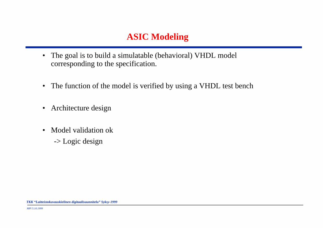
ASIC Modeling
• The goal is to build a simulatable (behavioral) VHDL modelcorresponding to the specification.
• The function of the model is verified by using a VHDL test bench
• Architecture design
• Model validation ok
-> Logic design

MPl 5.10.1999
TKK “Laitteistokuvauskielinen digitaalisuunnitelu” Syksy-1999
Logic design
• The goal is to write a synthezisable VHDL description of the design
• Design rules (Naming, vendor independence, Use only IEEE standardtypes, comments, …).
• Reusing
• Synchronous design !!
• Design partitioning (into RTL blocks)

MPl 5.10.1999
TKK “Laitteistokuvauskielinen digitaalisuunnitelu” Syksy-1999
Naming rules
• Use meaningful names for signals, ports, functions and parameters.For example, do not use ra for a RAM address bus. Instead, useram_addr or RamAddr (capital letters can also be used).
• If your design uses several parameters, use short but descriptivenames.
• Use the name clk for the clock signal. If there is more than oneclock in the design, use clk as the prefix for all clock signals (forexample clk4m, clk8m).
• Use the same name throughout the hierarchy for all clock signalsthat are driven from the same source.
• For active low signals, end the signal name with an underscorefollowed by a lowercase character x.
• Use the name reset for reset signals. For active low resets use thename reset_x.
• For multibit buses, use (y downto x) ordering of bits.

MPl 5.10.1999
TKK “Laitteistokuvauskielinen digitaalisuunnitelu” Syksy-1999
Naming rules
• Use the same name or similar names for ports and signals,throughout the hierarchy, that are connected. (for example, a => a;or a => a_int;)
• Use the name enab for an enable signal. If there is more than oneenable in the design, use enab as the prefix for all enable signals.
• Testbench is named 'name_of_the_block'_TB.

MPl 5.10.1999
TKK “Laitteistokuvauskielinen digitaalisuunnitelu” Syksy-1999
Guidelines for clocks and resets
The preferred clocking structure is a single global clockand positive edge-triggered flip-flops as the onlysequential devices.
clk
FF FF

MPl 5.10.1999
TKK “Laitteistokuvauskielinen digitaalisuunnitelu” Syksy-1999
Guidelines for clocks and resets
• Digital ASICs must be designed to be synchronous when possible.This must be considered, when VHDL for synthesis is written. Themain benefits of synchronous design are:
• Timing problems are avoided. Only the propagation of signalsto the next register during one clock cycle must be verified.
• Most of the problems with hazards are avoided.
• The X-states and glitches in gated and multiplexed clocks areavoided.
• It is easier to test a synchronous circuit than an asynchronousone.
• Static timing analysis is possible.

MPl 5.10.1999
TKK “Laitteistokuvauskielinen digitaalisuunnitelu” Syksy-1999
Guidelines for clocks and resets
• partition the design so that all the logic in a single module uses asingle clock and a single reset.
• Isolating clock and reset generation logic in a separate module allowsthe other modules to use the standard timing analysis and scaninsertion techniques. It also makes it easier to develop specific teststrategies for the clock/reset generation logic.
ClockGeneration
submodule1
submodule2
submodule3
clk1
clk2
clk3
master clock

MPl 5.10.1999
TKK “Laitteistokuvauskielinen digitaalisuunnitelu” Syksy-1999
Guidelines for clocks and resets
• Avoid gated clocks• Clock gating circuits tend to be technology specific and timing
dependent. Improper timing of a gated clock can generate a falseclock or glitch, causing a flip-flop to clock in the wrong data. Also,the skew of different local clocks can cause hold time violations.
• Gated clocks also cause limited testability because the logic clockedby a gated clock cannot be made part of a scan chain.
clk
FF FF

MPl 5.10.1999
TKK “Laitteistokuvauskielinen digitaalisuunnitelu” Syksy-1999
Guidelines for clocks and resets
• If your design requires gated clocks, use preferably vendor providedgated flip-flop elements using master clock.
masterclock
enable
reset
data

MPl 5.10.1999
TKK “Laitteistokuvauskielinen digitaalisuunnitelu” Syksy-1999
Guidelines for clocks and resets
• Avoid internally generated resets• Make sure your registers are controlled only by a single reset signal.• Avoid internally generated, conditional resets if possible. Generally,
all the registers in the macro should be reset at the same time. Thisapproach makes analysis and design much simpler and easier.
• If conditional reset is required, create a separate signal for the resetsignal, and isolate this in a separate module. This approach results inmore readable code and improves synthesis results.

MPl 5.10.1999
TKK “Laitteistokuvauskielinen digitaalisuunnitelu” Syksy-1999
Design partitioning
• Good partitioning in the design provides several advantagesincluding:
Easy handling of design requires sensible hierarchyBetter synthesis resultsFaster synthesis compile runtimesAbility to use simpler synthesis strategies to meet timingReusability

MPl 5.10.1999
TKK “Laitteistokuvauskielinen digitaalisuunnitelu” Syksy-1999
Design partitioning
• Locate related combinational logic in a single module and singleprocess if possible
• The synthesis tool has more flexibility in optimising a design whenrelated combinational logic is located in the same module. This isbecause synthesis tools cannot move logic across hierarchicalboundaries during compile operation.
clk COMB BFF A COMB CCOMB A clk FF C
A B C
clk FF A COMB A & B & C clk FF C
A C
Bad
Better
clk FF Aclk FF C
A C
COMB A & B & C Best

MPl 5.10.1999
TKK “Laitteistokuvauskielinen digitaalisuunnitelu” Syksy-1999
RTL block design
P t i t i RTLBl k
RTL Bl oc kD i
RTL Mode lI nt e gr a t i
Synt he s i z a bl eRTL Bl oc kD i
Synt he s i sCh k
RTL Bl oc kF t iV i f i t i
RTLBl kDoc ume nt a t i o
Bl oc kRe vi e w
VHDLSch.,DFD
A hiPl an/ De s c r i pt i
VHDL
RTL VHDL
Te x tdi
Ar c hi t e c t ur eM d l
Targettechnology
De s i gnC i l
Schematics
Sc he mat i ci
Tar ge th l dat a
b
simulation results
St i muliRe s pons e
Me nt orVSSSi l
VHDL TB
VHDL Te s t Be nc h
Te x tdi
VHDL,DFD
Adde d c omme nt s
RTL Block
Re l e as e d RTLbl k

MPl 5.10.1999
TKK “Laitteistokuvauskielinen digitaalisuunnitelu” Syksy-1999
Synthesis
S t h iPr e pa r a t i
LOGIC DESIGN
VERIFICATION
Modul eSynt he s i
Li bMa ppi ng
M d lOpt i mi z a t i
Ti mi ngA l i
SYNTHESIS VHDL
RTL VHDL Mode l
e . g .Te x t
di
VHDLSch.,DFD
RTL VHDL Mode lopt i mi z e d f or
h i
Schematics
Sc he mat i cibas e d on ge ne r i c
h l
Schematics
Sc he mat i ciadde d t e s t s t r uc t ur e
De s i gnCompi l e rTe s t Compi l e r
Generictechnology
Ge ne r i ch l dat a
b
Targettechnology
Tar ge th l dat a
b
Schematics
Sc he mat i ciopt i mi z e d f or t ar ge t
h l
Ti mi ngR
ASI C t e s ts ynt he s i s ,t t bi l i t
Schematics
Sc he mat i cibas e d on t ar ge t
h l

MPl 5.10.1999
TKK “Laitteistokuvauskielinen digitaalisuunnitelu” Syksy-1999
Gate level verification
Synthesis
Ne t l i s
Dat a She e td
Sy nt he s i sLi br ar
Sy nops y s De s i gn orFPGA
c ompi l e ror e qui v al e ntl
ASI C/ FPGAgat eLi b
ASI C/ FPGARTLd i i
Functional simulationTe s t be nc h,be h. mode l
St i mul idRe s pons e s
Static timing analysis
CHIP VERIFICATION
Netlist creator
VHDL/ gat e l e ve li l
Functional errors
Mapping (FPGA)
Floorplanning
Place&route (FPGA)
Timing simulationTe s t be nc h,be h. mode l
St i mul idRe s pons e s
VHDL/ gat e l e ve li l t
ASI C/ FPGA v e ndord it ool s
Timing errors
Ti mi ng
ASI C/ FPGACe l lLi b
Ti mi ng
Opt i mi z e ddb
Qui c k c he c k
Static timing analysis
FPGAi mpl eme nt at i
Mappi ngi nf or mat i
Fl oor pl anni ni nf or mat i
Aut omat i c / manualc ons t r ai n
TO TEST GENERATION
Formalverification
and
static timinganalyses
MPl 5.10.1999
TKK “Laitteistokuvauskielinen digitaalisuunnitelu” Syksy-1999
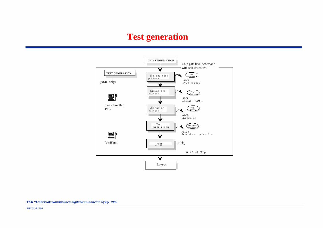
Test generation
Ma nua l t e s tpa t t e r n
t i
CHIP VERIFICATION
Layout
Aut oma t i ct tpa t t e r n
i
Te s tt i lSi mul a t i on
Fa ul tG di
TEST GENERATION
TestPattern
ASCI IManual : RAM . .
ASCI IAut omat i c
Test patternresponses
ASCI ITe s t dat a: s t i mul i +
Ve r i f i e d Chi ph i
Pr e l i m. t e s tpa t t e r n
t i(ASIC only)
Test CompilerPlus
ASCI IPr e l i mi nar y
TestPatterns
TestPattern
Chip gate level schematicwith test structures
VeriFault
MPl 5.10.1999
TKK “Laitteistokuvauskielinen digitaalisuunnitelu” Syksy-1999
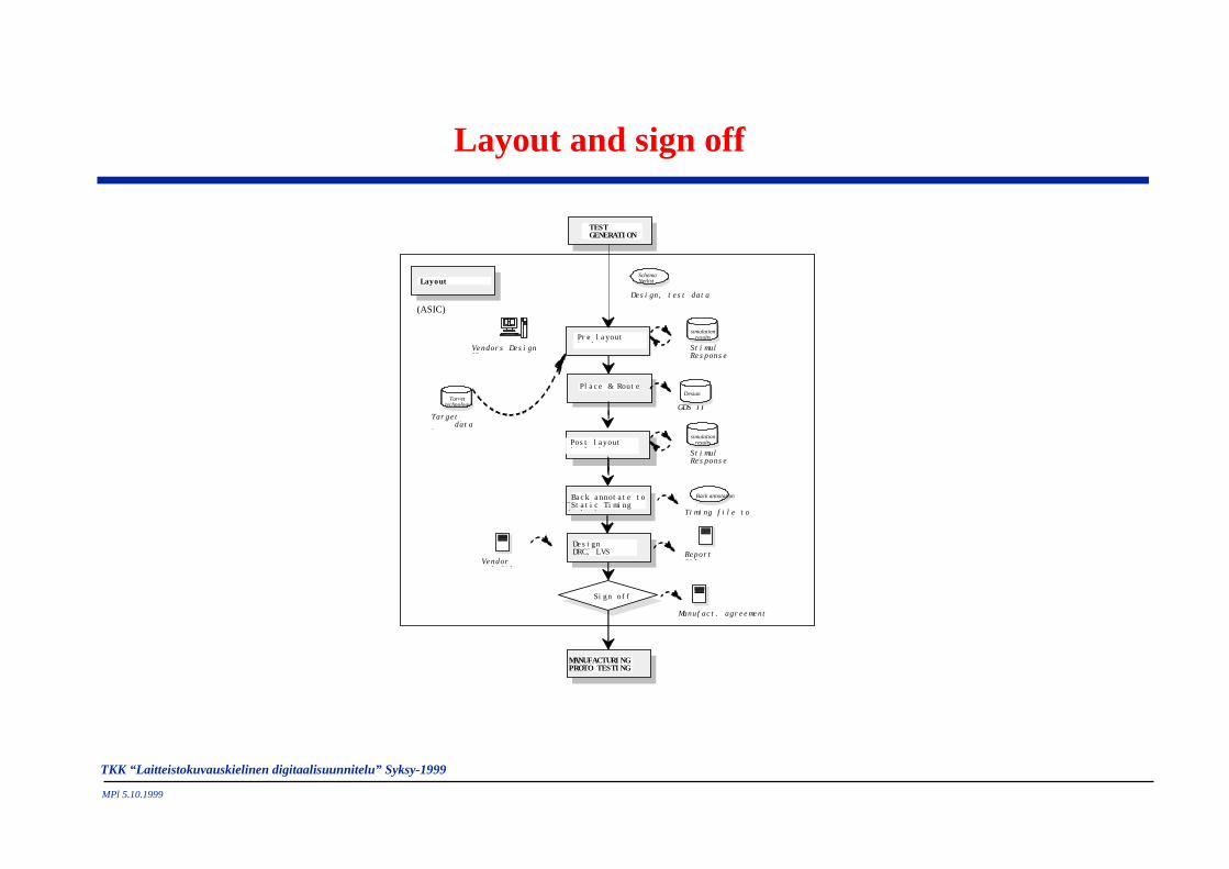
Layout and sign off
TEST GENERATI ON
Layout
MANUFACTURI NGPROTO TESTI NG
Pr e l a youti l t i
Pl a c e & Rout e
Ba c k a nnot a t e t oS St a t i c Ti mi ngA l i
De s i gni f i t i DRC, LVS
Si gn of f
SchemaNetlist
Des i gn, t es t dat a
GDS I I Targettechnology
Vendor s Des i gnKi
Tar ge th l dat a
bsimulation results
St i muliRes pons e
Back annotation
Ti mi ng f i l e t od i
Manuf ac t . agr e e me nt
(ASIC)
Design
Pos t l ayouti l t i
simulation results
St i muliRes pons e
Vendorl f i l
Repor tf i l

MPl 5.10.1999
TKK “Laitteistokuvauskielinen digitaalisuunnitelu” Syksy-1999
Prototype testing
• Final verification is done with E/S (engineering samples).
• Physical measurements:Parametric DC tests
Parametric AC tests
Functional tests
Power consumption
Thermal tests
• Release to system tests
• Final documentation and project completion
• Chips manufacturing

MPl 5.10.1999
TKK “Laitteistokuvauskielinen digitaalisuunnitelu” Syksy-1999
FPGA prototyping
• FPGA, Field Programmable Gate Array
• VHDL coding for FPGAs (design partitioning, limited maximumclock speed, limited amount of interfaces)
• Building prototyping board
• Prototyping in laboratory environment

MPl 5.10.1999
TKK “Laitteistokuvauskielinen digitaalisuunnitelu” Syksy-1999
FPGA prototyping
• Advantages:VHDL is tested with real clock speed, in real environment
Prototyping environment offers "early ASIC" for other projects
More secure to sign off
• DisadvantagesRequires a lot of time and resources
Expensive