Arithmetic Building Blocks - All...
29
ECE 261 James Morizio 1 Arithmetic Building Blocks • Datapath elements • Adder design – Static adder – Dynamic adder • Multiplier design – Array multipliers • Shifters, Parity circuits
Transcript of Arithmetic Building Blocks - All...

ECE 261 James Morizio 1
Arithmetic Building Blocks
• Datapath elements
• Adder design– Static adder
– Dynamic adder
• Multiplier design– Array multipliers
• Shifters, Parity circuits

ECE 261 James Morizio 2
A Generic Digital Processor
MEMORY
DATAPATH
CONTROL
Inp
ut-
Ou
tpu
t

ECE 261 James Morizio 3
Building Blocks for Digital Architectures
• Arithmetic unit
- Bit-sliced datapath (adder, multiplier, shifter, comparator, etc.)
• Memory
- RAM, ROM, Buffers, Shift registers
• Control
- Finite state machine (PLA, random logic.)
- Counters
• Interconnect
- Switches
- Arbiters
- Bus

ECE 261 James Morizio 4
Bit-Sliced Design
Bit 3
Bit 2
Bit 1
Bit 0
Control
Tile identical processing elements
Dat
a-in
Dat
a-out
Reg
iste
r
Adder
Shif
ter
Mult
ipli
er
Signals
Data Control
Metal 2
(control)
Metal 1
(data)

ECE 261 James Morizio 5
Single-Bit Addition
Half Adder Full Adder
0111
1001
1010
0000
SCoutBA
11111
01011
01101
10001
01110
10010
10100
00000
SCoutCBA
A B
S
Cout
A B
C
S
Cout
out
S A B
C A B
= ⊕
= g out( , , )
S A B C
C MAJ A B C
= ⊕ ⊕
=

ECE 261 James Morizio 6
Full-AdderA B
Cout
Sum
Cin
Fulladder

ECE 261 James Morizio 7
The Binary Adder
A B
Cout
Sum
Cin Fulladder
Sum = A ⊕ B ⊕ C
= ABCi + ABCi + ABCi + ABCi
Co = AB + BCi + ACi

ECE 261 James Morizio 8
Sum and Carry as a functions
of P, G
Define 3 new variable which ONLY depend on A, B
Gen erate (G) = AB
Prop agate (P) = A+B

ECE 261 James Morizio 9
The Ripple-Carry Adder
A0 B0
S0
Co,0Ci,0
A1 B1
S1
Co,1
A2 B2
S2
Co,2
A3 B3
S3
Co,3
(= Ci,1)FA FA FA FA
Wo rs t cas e d elay lin ear with th e n u mber o f b its
td = O(N)
Goal: Make the fas tes t poss ible carry path circuit
td = (N-1)tcarry + tsum

ECE 261 James Morizio 10
Complimentary Static CMOS Full
AdderVDD
VDD
VDD
VDD
A B
Ci
S
Co
X
B
A
Ci A
BBA
Ci
A B Ci
Ci
B
A
Ci
A
B
BA
28 Transistors
Note:
1) S = ABCi + Co(A + B + Ci)
2) Placement of Ci
3) Two inverter stages for
each Co
O(N) delay

ECE 261 James Morizio 11
Inversion Property
A B
S
CoCi FA
A B
S
CoCi FA
Inverting all inputs results in inverted outputs

ECE 261 James Morizio 12
Minimize Critical Path by Reducing
Inverting Stages
Co,0Ci,0 Co,1 Co,2 Co,3
FA’ FA FA’ FA
Odd CellEven Cell
Exploit Inversion Property
Need two different types of cells, FA’: no inverter in carry path
A0A1B0
A2B1 B2
B3A3
S0 S1 S2 S3

ECE 261 James Morizio 13
A better structure: the Mirror
Adder
VDD
Ci
A
BBA
B
A
A B
Kill
Generate"1"-Propagate
"0"-Propagate
VDD
Ci
A B Ci
Ci
B
A
Ci
A
BBA
VDD
SCo
24 transistors

ECE 261 James Morizio 14
The Mirror Adder
• Symmetrical NMOS and PMOS chains – identical rising and falling transitions if the NMOS and PMOS devices are
properly sized.
– Maximum of two series transistors in the carry-generation circuitry.
• Critical issue: minimization of the capacitance at Co. – Reduction of the diffusion capacitances important.
– The capacitance at Co composed of four diffusion capacitances, two
internal gate capacitances, and six gate capacitances in the connecting
adder cell .
• Transistors connected to Ci placed closest to output.
• Only the transistors in carry stage have to be optimized for
speed. All transistors in the sum stage can be minimal size.

ECE 261 James Morizio 15
NP-CMOS Adder
VDD
φ
φ
Ci0
A0 B0 B0
φ
A0
VDD
φ
B1
φ
A1
VDD
φ
φ
A1 B1
Ci1
Ci2
Ci0
Ci0
B0
A0B0
S0
A0
VDD
φ
φ
VDD
φ
VDD
φ
φ
B1 Ci1
B1
φ
A1A1
VDD
φS1
Ci1
Carry Path
17 transistors,
ignoring extra
inverters for inputs
and outputs

ECE 261 James Morizio 16
Manchester Carry Chain
P0
Ci,0
P1
G0
P2
G1
P3
G2
P4
G3 G4
VDD
∅∅∅∅
∅∅∅∅
Co,4
• Only nMOS transmission gates used. Why?
• Delay of long series of pass gates: add buffers

ECE 261 James Morizio 17
Carry-Bypass Adder
FA FA FA FA
P0 G1 P0 G1 P2 G2 P3 G3
Co,3Co,2Co,1Co,0Ci,0
FA FA FA FA
P0 G1 P0 G1 P2 G2 P3 G3
Co,2Co,1Co,0Ci,0
Co,3
BP=P oP1P2P3
Idea: If (P0 and P1 and P2 and P3 = 1)
then Co3 = C0, else “kill” or “generate”.

ECE 261 James Morizio 18
Manchester-Carry Implementation
P0
Ci,0
P1
G0
P2
G1
P3
G2
BP
G3
BP
Co,3
ECE 261 James Morizio 19
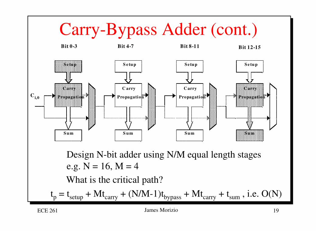
Carry-Bypass Adder (cont.)
S e tu p
C arry
Propagation
S um
S e tu p
C arry
Propagation
S um
Setup
C arry
Propagation
Sum
S e tu p
C arry
Propagation
S um
Bit 0-3 Bit 4-7 Bit 8-11 Bit 12-15
Ci,0
Design N-bit adder using N/M equal length stages
e.g. N = 16, M = 4
What is the critical path?
tp = tsetup + Mtcarry + (N/M-1)tbypass + Mtcarry + tsum , i.e. O(N)

ECE 261 James Morizio 20
Carry Ripple versus Carry Bypass
N
tp
ripple adder
bypass adder
4..8

ECE 261 James Morizio 21
Carry-Select Adder
Setup
"0" Carry Propagation
"1" Carry Propagation
Multiplexer
Sum Generation
Co,k-1 Co,k+3
"0"
"1"
P,G
Carry Vector
Generate carry out for both “0” and “1” incoming carries
4-bit block for bits
k, k+1, k+2, k+3

ECE 261 James Morizio 22
Carry Select Adder: Critical Path
Setup
"0" Carry
"1" Carry
Multiplexer
Sum Generation
"0"
"1"
Setup
"0" Carry
"1" Carry
Multiplexer
Sum Generation
"0"
"1"
Setup
"0" Carry
"1" Carry
Multiplexer
Sum Generation
"0"
"1"
Setup
"0" Carry
"1" Carry
Multiplexer
Sum Generation
"0"
"1"
Bit 0-3 Bit 4-7 Bit 8-11 Bit 12-15
S0-3 S4-7 S8-11 S12-15
Co,15Co,11Co,7Co,3Ci,0

ECE 261 James Morizio 23
Carry-Select Adder: Linear Configuration
Setup
"0" Carry
"1" Carry
Multiplexer
Sum Generation
"0"
"1"
Setup
"0" Carry
"1" Carry
Multiplexer
Sum Generation
"0"
"1"
Setup
"0" Carry
"1" Carry
Multiplexer
Sum Generation
"0"
"1"
Setup
"0" Carry
"1" Carry
Multiplexer
Sum Generation
"0"
"1"
Bit 0-3 Bit 4-7 Bit 8-11 Bit 12-15
S0-3 S4-7 S8-11 S12-15
Co,15Co,11Co,7Co,3Ci,0
(1)
(5)(5)(5)(6)
(1)
(7) (8)(5)(5)
Are equal-sized blocks best?

ECE 261 James Morizio 24
Linear Carry Select
Setup
"0" Carry
"1" Carry
Multiplexer
Sum Generation
"0"
"1"
Setup
"0" Carry
"1" Carry
Multiplexer
Sum Generation
"0"
"1"
Setup
"0" Carry
"1" Carry
Multiplexer
Sum Generation
"0"
"1"
Setup
"0" Carry
"1" Carry
Multiplexer
Sum Generation
"0"
"1"
Bit 0-3 Bit 4-7 Bit 8-11 Bit 12-15
S0-3 S4-7 S8-11 S12-15
Co,15Co,11Co,7Co,3Ci ,0

ECE 261 James Morizio 25
Square Root Carry Select
Setup
"0" Carry
"1" Carry
Multiplexer
Sum Generation
"0"
"1"
Setup
"0" Carry
"1" Carry
Multiplexer
Sum Generation
"0"
"1"
Setup
"0" Carry
"1" Carry
Multiplexer
Sum Generation
"0"
"1"
Setup
"0" Carry
"1" Carry
Multiplexer
Sum Generation
"0"
"1"
Co,15Co,11Co,7Co,3Ci ,0
(1)
(4)(3)(3)(4)
(1)
(5) (6)(6)(5)
Bit 0-1 Bit 2-4 Bit 5-8 Bit 9-13
i.e., O(√N)

ECE 261 James Morizio 26
Adder Delays - Comparison
0.0 20.0 40.0 60.0
N
0.0
10.0
20.0
30.0
40.0
50.0
tp
ripple adder
linear select
square root select

ECE 261 James Morizio 27
Carry Look-Ahead - Basic Idea
A0,B0 A1,B1 AN-1,BN-1...
Ci,0 P0 Ci ,1 P1Ci,N-1 PN-1
...
Delay “independent” of the number of bits
S0S1
SN-1

ECE 261 James Morizio 28
Carry-Lookahead Adders• High fanin for large N
• Implement as CLA slices, or use 2nd level lookahead
generator
4
4
4 4 4
4 4 4 4 4 4 4 16-bit CLA based on 4-bit
slices and ripple carry
4
4
4 4 4
4 4 4 4 4 4 4
CLA generator
Faster
implementation

ECE 261 James Morizio 29
Look-Ahead: TopologyVDD
Gnd
G3
G2
G1
G0
P0
P3
P2
P1
Ci,0
Co,3


![10/09/11 Il mondo si muove se noi ci muoviamo, si muta se noi ci mutiamo, si fa nuovo se alcuno si fa nuova creatura […] Lordine nuovo comincia se qualcuno.](https://static.fdocuments.net/doc/165x107/5542eb59497959361e8c601c/100911-il-mondo-si-muove-se-noi-ci-muoviamo-si-muta-se-noi-ci-mutiamo-si-fa-nuovo-se-alcuno-si-fa-nuova-creatura-lordine-nuovo-comincia-se-qualcuno.jpg)