
Areviewofdesignconsiderationsforthesensormatrixin ...seidel/Article.pdf · UNCORRECTED PROOF...
30
UNCORRECTED PROOF Nuclear Instruments and Methods in Physics Research A 0 (2001) 1–30 A review of design considerations for the sensor matrix in semiconductor pixel detectors for tracking in particle physics experiments Sally Seidel* New Mexico Center for Particle Physics, Department of Physics and Astronomy, University of New Mexico, 800 Yale Blvd NE, Albuquerque, NM 87131 USA Received 9 December 2000; accepted 26 January 2001 Abstract Methods have been developed to improve the reliability of silicon sensors, in particular for pixel detectors, and their resistance to radiation damage, as it is encountered in tracking detectors in particle physics experiments. The choice of wafer material, the processing techniques, and the sensor layout are discussed. Alternative semiconductor substrates and variations on the planar hybrid design are mentioned. # 2001 Published by Elsevier Science B.V. PACS: &; &; & Keywords: &; &; & 1. Introduction The principal focus of this paper is the design of the silicon sensor part of a pixel detector. Originally, the included material was part of a full-day course on active pixel detectors. The other lectures treated the electronic readout chips, the hybrid interconnection technologies, and applica- tions. The development of pixel sensors is an extension to two dimensions of the silicon microstrip sensor technology, many of the features of which are described in Refs. [1,2]. This two-dimensional approach requires innovation in interconnections and electronics signal processing not described here. A silicon pixel sensor is defined here to be the sensing element of a hybridized detector, including a lightly doped substrate (usually n-type), one of whose surfaces is in contact with highly doped silicon of the opposite type (correspondingly, p- type), thereby forming a junction. The opposite side of the silicon wafer is in direct contact with highly doped silicon of the same type as the bulk. The highly doped silicon will be referred to here as ‘‘the implants’’, although in fact it can be introduced through implantation or diffusion. The implants on both sides of the device can be electrically contacted. When a reverse bias voltage V B is placed across them, a region in the bulk silicon is depleted of free charge carriers. The width W of the depletion region in the n-type bulk 1 3 5 7 9 11 13 15 17 19 21 23 25 27 29 31 33 35 37 39 41 43 45 47 49 51 53 55 57 59 61 63 65 NIMA : 40923 - PROD.TYPE: COM ED: MALLIKARJUNA PAGN: BALA // BVR SCAN: MALLI pp.1^30 (col.¢g.: NIL) *Tel.: 505-277-2616; fax: 505-272-1520. E-mail address: [email protected] (S. Seidel). 0168-9002/01/$ - see front matter # 2001 Published by Elsevier Science B.V. PII:S0168-9002(01)00695-7
Transcript of Areviewofdesignconsiderationsforthesensormatrixin ...seidel/Article.pdf · UNCORRECTED PROOF...
UNCORRECTED PROOF
Nuclear Instruments and Methods in Physics Research A 0 (2001) 1–30
A review of design considerations for the sensor matrix insemiconductor pixel detectors for tracking in particle physics
experiments
Sally Seidel*
New Mexico Center for Particle Physics, Department of Physics and Astronomy, University of New Mexico,
800 Yale Blvd NE, Albuquerque, NM 87131 USA
Received 9 December 2000; accepted 26 January 2001
Abstract
Methods have been developed to improve the reliability of silicon sensors, in particular for pixel detectors, and theirresistance to radiation damage, as it is encountered in tracking detectors in particle physics experiments. The choice of
wafer material, the processing techniques, and the sensor layout are discussed. Alternative semiconductor substratesand variations on the planar hybrid design are mentioned. # 2001 Published by Elsevier Science B.V.
PACS: &; &; &
Keywords: &; &; &
1. Introduction
The principal focus of this paper is the design ofthe silicon sensor part of a pixel detector.Originally, the included material was part of afull-day course on active pixel detectors. The otherlectures treated the electronic readout chips, thehybrid interconnection technologies, and applica-tions.
The development of pixel sensors is an extensionto two dimensions of the silicon microstrip sensortechnology, many of the features of which aredescribed in Refs. [1,2]. This two-dimensionalapproach requires innovation in interconnections
and electronics signal processing not describedhere. A silicon pixel sensor is defined here to be thesensing element of a hybridized detector, includinga lightly doped substrate (usually n-type), one ofwhose surfaces is in contact with highly dopedsilicon of the opposite type (correspondingly, p-type), thereby forming a junction. The oppositeside of the silicon wafer is in direct contact withhighly doped silicon of the same type as the bulk.The highly doped silicon will be referred to here as‘‘the implants’’, although in fact it can beintroduced through implantation or diffusion.
The implants on both sides of the device can beelectrically contacted. When a reverse bias voltageVB is placed across them, a region in the bulksilicon is depleted of free charge carriers. Thewidth W of the depletion region in the n-type bulk
1
3
5
7
9
11
13
15
17
19
21
23
25
27
29
31
33
35
37
39
41
43
45
47
49
51
53
55
57
59
61
63
65
NIMA :40923 - PROD.TYPE: COM ED:MALLIKARJUNAPAGN: BALA //BVR SCAN:MALLI
pp.1^30 (col.¢g.: NIL)
*Tel.: 505-277-2616; fax: 505-272-1520.
E-mail address: [email protected] (S. Seidel).
0168-9002/01/$ - see front matter # 2001 Published by Elsevier Science B.V.
PII: S 0 1 6 8 - 9 0 0 2 ( 0 1 ) 0 0 6 9 5 - 7
UNCORRECTED PROOF
is given by
W ¼
ffiffiffiffiffiffiffiffiffiffiffiffiffiffiffiffiffiffiffiffiffiffiffiffiffiffiffiffiffiffiffiffiffiffi2eVB
qNdð1þNd=NaÞ
s
where e is the silicon dielectric constant, q is thecharge, and Nd and Na are the donor and acceptorconcentrations, respectively. Typical sensors usedfor particle physics applications utilize bulk siliconof Nd � 1012 atoms=cm3 and implanted silicon ofdopant density greater than 1014 atoms=cm3.
To form a pixel sensor, the implant on one ofthe sides of the wafer must be segmented intoregions, called pixels, each of which is ultimatelyattached to its own preamplifier circuit to form anindividual channel of the detector. Typical dimen-sions of an individual pixel are such that its area isa number on the order of 2� 104 mm2. When sucha pixel sensor is placed in the path of a chargedparticle, the traversing particle produces electron–hole pairs through ionization along the length ofits track in the silicon. If the sensor is adequatelydepleted, the electrons will drift to the n-typeimplants, and the holes to the p, from either ofwhich appropriate electronics can read the signalsout. Interpolation between signals from differentchannels, either on the basis of their time or theirpulseheight, provides information about the pathof the traversing particle. Depletion of intrinsicsilicon bulk essentially eliminates the free carriers(which, with a density of about 1:45� 1010 cm�3,outnumber the signal carriers by four orders ofmagnitude).
The usual environment in which pixel detectorsare operated for particle physics applications isone of high luminosity and close proximity to theinteraction point or particle source. The highluminosity is required for sensitivity to rare events;it often, however, implies high radiation damage.Close proximity permits precision tracking andallows on-line triggers to examine tracks whiletheir curvature is small, often simplifying recon-struction algorithms and speeding trigger deci-sions. Increased proximity exacerbates radiationdamage, however. Furthermore, as particle trackdensity is highest near the production point, atracker’s granularity must be increased as itsdistance from the interaction point is diminished.
The desire for fine granularity makes silicondetectors a natural choice for tracking; however,while the very small feature size available in silicondevices provides low capacitance, low noise,consequently good signal-to-noise ratio, and lowoccupancy per channel (which reduces eventbuffering requirements), the radiation damage,which increases capacitance and creates chargetraps, must be addressed in the design. Pixels’small feature size and typically harsher radiationenvironment have placed constraints upon pixeldesign beyond those required for strip sensors;these are a subject central to this paper. Specifi-cally, pixel sensor design and development haveborrowed what was useful from silicon strip sensordesign while focusing on the following issues: (1)engineering for robustness of radiation-damagedsensors designed with proven technologies; (2)maximizing the radiation hardness availablethrough new technologies; (3) minimizing thesensors’ capacitance and maximizing their signalcollection; and (4) exploring new design concepts.Because so many aspects of silicon pixel sensordesign are influenced by radiation hardnessrequirements, the first section of the paper brieflyreviews the response of silicon to radiation. Thefirst section is not intended to be a complete reviewof radiation damage effects, but is merely intendedto provide foundational information upon whichspecific design choices described in subsequentsections are based.
2. Radiation damage in silicon
2.1. Introduction
Radiation damage is caused by the passage ofparticles through the sensor. The main source ofcharged particles is collisions at the interactionpoint, so their fluence is proportional to r�2. Themain source of neutrons is backsplash from thecalorimeter, so their fluence depends on theapparatus shielding and design. Bulk and surfacedamage are induced by different mechanisms, sothese are considered separately below. The symbolF is used here to represent fluence. An excellent
1
3
5
7
9
11
13
15
17
19
21
23
25
27
29
31
33
35
37
39
41
43
45
47
49
51
53
55
57
59
61
63
65
67
69
71
73
75
77
79
81
83
85
87
89
91
93
95
S. Seidel / Nuclear Instruments and Methods in Physics Research A 0 (2001) 1–302
NIMA :40923 -

UNCORRECTED PROOF
recent review of radiation damage effects in siliconmay be found in Ref. [3].
2.2. Bulk damage
Particles passing through a silicon substrate cancause dislocations in the lattice that alter the bandstructure. Following the collision, the displacedatom (or Primary Knock-on Atom, PKA) be-comes a silicon interstitial and leaves a vacancy.The combination of vacancy and interstitial atomis known as a Frenkel Pair. In silicon, approxi-mately 25 eV are required to displace the PKA [4].The semiconductor bulk damage model postulatesthat the recoiling PKA strikes neighboring latticeatoms, and if its energy is greater than about2 keV; its action will lead to the formation ofclustered damage sites of typical volume 10�19 cm3
[5]. Interstitial atoms and vacancies that escape acluster and migrate through the lattice aregenerally trapped at the impurity atoms and formpoint defects. The subsequent evolution of theclusters and=or point defects is thought to producecertain macroscopic effects that are describedbelow.
The damage done by radiation to silicondepends upon the type and energy of the radiation.The bulk damage is generally thought to dependexclusively on the non-ionizing energy loss(‘‘NIEL’’) of the particle. This fact, which hasbeen demonstrated to be the case over 14 orders ofmagnitude in particle energy, is called the NIELhypothesis. (Some deviation may be apparent inthe case of oxygenated silicon substrates; seeSection 5.2.3 below.) It is consequently possibleto scale the damage caused by different particlespecies at various energies by the NIEL, or by anequivalent scale factor known as the displacementdamage function. The displacement damage func-tion, which may be calculated by combining theindividual reaction cross-section, the energy dis-tribution of recoils produced by that reaction, andinformation about the partition between ionizingand non-ionizing energy loss of the recoils, andthen summing over all reaction channels availableto the initial particle at its energy, is shown inFig. 1 (from Ref. [6]) as a function of particlespecies and energy. The portion of the spectrum
below 190 eV is due to neutron capture and is notexpected to be significant for LHC and futureTevatron experiments.
To facilitate comparisons between experimentsand radiation sources, fluences are usually ex-pressed in terms of the equivalent damage done by1 MeV neutrons; in this paper the symbol hnirepresents the 1 MeV neutron equivalent. Pionscause the worst damage to silicon in nuclear andparticle physics experiments through D-resonanceproduction in the pion–nucleus interaction.
2.3. Surface damage
Bulk silicon naturally develops a layer of silicondioxide, SiO2. Bulk damage to the oxide has anegligible effect on its electrical properties becauseoxides, intrinsically quite disordered by theirproduction process, contain a large number ofdefects even when unirradiated. In oxides, themost significant damage is caused by ionizingradiation, which generates bound charge in theoxide layer and at the interface between the siliconand the silicon dioxide. Because electrons havesignificantly higher mobility than holes in SiO2,ionization-induced electrons rapidly diffuse out ofthe oxide, leaving behind a relatively permanentand immobile population of holes. The oxide chargehas been observed [7] to saturate after about 100krad at a value of about 3� 1012 cm�2 in deviceswith detector-quality oxide. The explanation for this
1
3
5
7
9
11
13
15
17
19
21
23
25
27
29
31
33
35
37
39
41
43
45
47
49
51
53
55
57
59
61
63
65
67
69
71
73
75
77
79
81
83
85
87
89
91
93
95
Fig. 1. Displacement damage functions for neutrons, protons,
pions, and electrons. Reprinted from Ref. [6] with permission.
S. Seidel / Nuclear Instruments and Methods in Physics Research A 0 (2001) 1–30 3
NIMA :40923 -

UNCORRECTED PROOF
is thought to be the limited number of permanenttrap sites available in the oxide. No saturation ofbulk effects has been observed up to fluences of afew times 1015hni cm�2 [8].
In general the macroscopic effects of bulkdamage are harder to control and more lethal[9–11] to sensors than are the effects of surfacedamage; they have consequently received moreattention.
2.4. Macroscopic effects of radiation damage insemiconductors
2.4.1. IntroductionRadiation damage to the bulk of the sensor
consists in defects in the crystal lattice. Suchdefects have associated energy levels in the middleregion of the forbidden energy band gap. Thedefect levels act as generation-recombinationcenters for positive and negative charge carriers,leading to increase in diode dark current, signalloss by temporary trapping, change in the effectivedopant concentration, and increased resistivity ofthe undepleted part of the diode. Each of theseeffects is described below.
2.4.2. Leakage currentEmpirically
JðFÞ ¼ aFþ Jintrinsic
where J and Jintrinsic are volume leakage currentdensities, F is fluence, and a is the current-relateddamage constant which will be described furtherbelow. Current Ileakage increases in response to thedevelopment of generation-recombination centersin the band gap. It causes stochastic noise ENC inthe pixel’s amplifier such that
ENC /ffiffiffiffiffiffiffiffiffiffiffiffiffiffiffiffiffiffiffiffiffiffiffiffiffiffiffiffiffiffiffiffiffiIleakage � tshaping
pwhere tshaping is shaping time. If uncontrolled, heatassociated with this leakage current can lead tothermal runaway.
The leakage current, which depends on tem-perature through the damage constant a, isobserved to change after the irradiation is overthrough a process called annealing. The relation-ship between a, the temperature T at which the
irradiation occurs, and time t can be parameterizedas [12]
aðT ; tÞ ¼ a1e�t=t1ðTÞ þ a0 � b lnðyðTÞt=t0Þ
where t0 is the reference time associated with theduration of the irradiation, t1 is the characteristictime associated with the annealing, and a0, a1, andb are annealing functions given in Table 1. Theparameter yðTÞ is defined by
yðTÞ ¼ expEI
kB
1
TR�
1
T
� �� �:
In this equation, kB is Boltzmann’s constant, TR
is the reference temperature to which the measure-ment is normalized, and EI is the activationenergy. A complete description of the physicalprocesses behind annealing does not yet exist. It isexpected to involve multiple interactions betweendefects and defect complexes, or the dispersal ofcomplexes into point defects, each of which maybe activated or deactivated at different tempera-tures. A useful table of important defects insilicon, and their properties, may be found inRef. [2]. The empirical formula above for a fits wellto data from a variety of processes and irradiationlevels, as may be seen from Fig. 2.
2.4.3. Dopant concentrationThe effective dopant concentration, Neff , of the
substrate reflects the combination of ionizedshallow levels and charged deep levels that ispresent. The effect of radiation is thought to beassociated with the removal of shallow levels bycreation of defect complexes and introduction ofdeep donors and acceptors. Neff has been shown tovary with fluence F over time t for temperature T
1
3
5
7
9
11
13
15
17
19
21
23
25
27
29
31
33
35
37
39
41
43
45
47
49
51
53
55
57
59
61
63
65
67
69
71
73
75
77
79
81
83
85
87
89
91
93
95
Table 1
Parameters associated with current annealing at temperature
TA ¼ 608C (from Ref. [12])
Parameter Units Value
a1 �10�17 A=cm 1:01� 0:38t1 Minutes 93� 24
a0 �10�17 A=cm 5:03� 0:09b �10�18 A=cm 3:34� 0:26t0 Minutes 1
S. Seidel / Nuclear Instruments and Methods in Physics Research A 0 (2001) 1–304
NIMA :40923 -

UNCORRECTED PROOF
according to the expression [13]
Neff ðFÞ ¼ Neff0 þNC þNaðF; t;TÞ þNY:
Here
NC � NC0ð1� e�cFÞ þ gCF
is known as the stable damage coefficient becauseit does not depend upon time; Na, the short-termbeneficial annealing coefficient, may be parameter-ized as a sum of exponentials
Na ¼ FXi
ga;ie�t=ta;iðTÞ:
Experiments performed at room temperature [14]found this component to be insignificant after 2days; elevated temperature studies [15] found onlyone exponential component to be detectable after5 min.
The NY term is the ‘‘reverse annealing’’ or ‘‘anti-annealing’’ coefficient. Formerly parameterized asgYFð1� e�t=tY Þ, it has now been shown [16] to be afirst-order effect in defect concentration and isbetter expressed as
NY � gYF 1�1
1þ t=tY
� �:
Here tY is the time constant given empirically [17]by tY ¼ 9140e�0:152T , where T is temperature inCelsius degrees. This term has been the subject of
considerable research because of the property thatit can attain values significantly larger than thepre-irradiation dopant density as t ! 1. Theparameter Neff0 represents the dopant concentra-tion in the unirradiated substrate, NC0 and c areparameters associated with partial donor removal,gC is the stable acceptor parameter, and gY is theanti-annealing coefficient. Table 2 summarizesvalues from a recent fit [18] for each of theannealing parameters. Fig. 3 illustrates the effectof each of the three annealing terms on theeffective dopant concentration; after a period oftime on the order of months has elapsed sinceirradiation, the dopant concentration of an irra-diated sensor can be several times what it wasboth prior to irradiation and immediately afterthe conclusion of the irradiation. The fluence-dependent change in dopant concentration has
1
3
5
7
9
11
13
15
17
19
21
23
25
27
29
31
33
35
37
39
41
43
45
47
49
51
53
55
57
59
61
63
65
67
69
71
73
75
77
79
81
83
85
87
89
91
93
95
Fig. 2. Values of a as a function of annealing time at 608C for
diodes. The leakage current was measured at room temperature
and normalized to 208C. The legend indicates the neutron
fluence and the manufacturers. Reprinted from Ref. [12] with
permission from Elsevier Science.
Table 2
Best-fit parameters for the annealing constants of Section 2.4.3,
extracted from measurements on sensors fabricated from high-
resistivity n-type float zone silicon (from Ref. [18])
Parameter Value Activation energy (eV)
gA ð1:92� 0:05Þ � 10�2=cm 1:09� 0:09gY ð5:16� 0:09Þ � 10�2=cm 1:31� 0:04gC ð1:49� 0:03Þ � 10�2=cm }
NC0 ð0:6020:90Þ �Neff0 }
c ð123Þ � 10�13 cm2 }
Fig. 3. An example of the annealing behavior of the radiation-
induced change in the effective doping concentration,
DNeff � Neff �Neff0. The sample was irradiated with a neutron
fluence of 1:4� 1013 cm�2 and annealed at a temperature of
608C. Reprinted from Ref. [18] with permission from Elsevier
Science.
S. Seidel / Nuclear Instruments and Methods in Physics Research A 0 (2001) 1–30 5
NIMA :40923 -

UNCORRECTED PROOF
significant impact on the behavior of the sensor’sdepletion voltage. This connection will bediscussed in Section 3.1.
2.4.4. Annealing‘‘Annealing’’ is the term used above for the
change in both the effective dopant concentration(equivalently, depletion voltage) and the leakagecurrent with time after the irradiation process hasstopped. This process occurs in both p- and n-typesubstrates and is independent of material type (i.e.,float zone, Czochralski, or epitaxial silicon) andinversion status (see Section 3.7). Table 3, takenfrom Ref. [12], illustrates the universality of theannealing parameter a.
There is neither universal agreement amongexperimenters about whether the changes involtage and current are due to the same micro-scopic process, nor about exactly what thatprocess is. One opinion holds that the effects aredue to deep acceptor creation and possibly donorremoval (see, for example, Ref. [14]). Someinvestigators ascribe them to donor compensationby deep acceptors only [19]. The effort to associatethe macroscopic changes in voltage and currentwith specific defects is a very active field of inquiryand uses a variety of spectroscopic methods. Foran introduction to some of these inquiries, seeRefs. [20–22]. While there has not yet been anunambiguous connection demonstrated between
the presence of a specific defect and the observa-tion of a specific change to the electrical characterof a silicon sensor, recent results in Deep LevelTransient Spectroscopy and Thermally StimulatedCurrent measurements support the conjecture thatreverse annealing comes from the rearrangementof interstitial defects.
2.4.5. Charge trappingTrapping occurs when crystal defects produce
local energy states within the band gap. A trap’saverage capture time increases exponentially withits depth and varies inversely with the capturecross-section. Defects with multiple energy levelscan act simultaneously as traps for electrons andholes, in general with different associated trappingtimes. In systems for which the electron and holecapture probabilities differ, a positional (depth)dependence of the signal amplitude arises. Theaverage time during which a signal charge istrapped in a semiconductor is given by
t ¼ eðEd�EiÞ=kBTÞ=svthermalni
where Ed � Ei is the difference between the defectand intrinsic energy levels, kB is Boltzmann’sconstant, T is temperature, s is the capture cross-section, vthermal is the thermal velocity of the chargecarriers, and ni is the intrinsic carrier concentra-tion. The relation between trap (defect) con-centrations and fluence is given in Section 2.4.3.
1
3
5
7
9
11
13
15
17
19
21
23
25
27
29
31
33
35
37
39
41
43
45
47
49
51
53
55
57
59
61
63
65
67
69
71
73
75
77
79
81
83
85
87
89
91
93
95
Table 3
Measured values of a for a variety of materials. The oxygen and carbon concentrations are both given in units of 1016 cm�3. The units
of a are 10�17=A=cm. Details of the technologies used for manufacturing the diodes may be found in Ref. [12]
Crystal Producer crystal Producer diode Guard ring r (kO cm) [O] [C] að80 min;608CÞ
n-FZ Wacker MPI Yes 2.7 55 50:5 3:99� 0:14n-FZ Wacker ELMA Yes 10–20 55 50:5 4:01� 0:04n-FZ Wacker ITE Yes 4.0 50:02 53 3:87� 0:07n-FZ Wacker ITE Yes 0.42 510 52 4:02� 0:11n-FZ Topsil Sintef Yes 6.6 55 50:5 4:14� 0:06n-FZ ITME ITE Yes 0.78 17 52 3:79� 0:08n-FZ ITME ITE Yes 0.11 510 2 3:61� 0:11n-FZ ITME HH No 0.13 510 2 3:93� 0:13n-Cz Polovodice HH No 0.14 90 0.5 3:94� 0:18p-EPI ITME DIOTEC No 0.4 4–20 1–2 4:41p-EPI ITME DIOTEC No 1.6 3–20 1–2 3:92� 0:19p-EPI ITME DIOTEC No 3.9 4–60 1–2 4:06� 0:40
S. Seidel / Nuclear Instruments and Methods in Physics Research A 0 (2001) 1–306
NIMA :40923 -

UNCORRECTED PROOF
Trapping has implications both for signal loss anddetector noise (see Section 3.6).
2.4.6. Conductivity of the undepleted bulkMeasurements [23] of the resistivity of the
undepleted bulk of silicon devices show that itincreases by more than a factor of 10 (from about35 kO cm to about 400 kO cm) during an irradia-tion to 1013hni cm�2 (see Fig. 4, which concernsn-type float zone material). This effect has beeninterpreted [24] as an indication of the relativeposition of the Fermi level EF of the damagedsilicon and the silicon intrinsic energy level Ei,which are related to the resistivity r through
1
r¼ qniðmne
ðEF�EiÞ=kBT þ mpeðEi�EFÞ=kBT Þ;
where q is the magnitude of the carrier charge, mi iscarrier mobility for type i, ni is the intrinsic carrierconcentration, kB is Boltzmann’s constant, and Tis temperature. Ref. [24] emphasizes that the factthat radiation-induced defects are deep rather thanshallow influences the probability of defect ioniza-tion and leads to the more complicated expressionfor resistivity given above rather than the simplercorrespondence between r and the voltage-to-current ratio.
3. Consequences of radiation damage for the
operation of silicon sensors
3.1. Depletion voltage
Section 2.4.3 introduced the relationshipbetween fluence, F, and effective dopant concen-tration, Neff . The depletion voltage of the sensor,VdepðFÞ, is related to these through the electricalresistivity, r, such that
VdepðFÞ ¼w2
2emrðFÞ
for
rðFÞ ¼1
qmNeff ðFÞ:
Here w is sensor thickness, e is electrical permit-tivity, m is carrier mobility, and q is electric charge.
If one combines these relations with those inSection 2.4.3, taking care with signs, one finds thatwhen n-type silicon is subjected to radiation, itinitially decreases its Neff until it becomes quasi-intrinsic, then undergoes an apparent change oftype from n to p (this is called type inversion), andsubsequently increases its Neff , and consequentlyits Vdep, without limit. In the case of a sensor thatis initially p-type, the unlimited increase of Neff
and Vdep begins immediately with irradiation, andno type inversion occurs. Fig. 5 shows the beha-vior of jNeff j and Vdep as a function of fluence.
The relationship between Vdep and fluencemeans that a detector must be operated partially
1
3
5
7
9
11
13
15
17
19
21
23
25
27
29
31
33
35
37
39
41
43
45
47
49
51
53
55
57
59
61
63
65
67
69
71
73
75
77
79
81
83
85
87
89
91
93
95
Fig. 5. The depletion voltage and magnitude of the effective
dopant concentration of bulk silicon as a function of fluence, as
measured immediately after irradiation. Reprinted from Ref.
[14] with permission from Elsevier Science.
Fig. 4. The neutron-induced resistivity change, in n=cm2, in the
electrically neutral bulk of a high-resistivity silicon sample.
Reprinted from Ref. [23] with permission from Elsevier Science.
S. Seidel / Nuclear Instruments and Methods in Physics Research A 0 (2001) 1–30 7
NIMA :40923 -

UNCORRECTED PROOF
depleted once the depletion voltage exceeds thebreakdown voltage. Operation in this moderequires attention to several issues. First, in thedepleted region, signal collection on the junctionside is rapid: the n-side (electron) signal is collectedin about 8 ns. The p-side (hole) signal is collectedin about 21 ns due to the fact that hole mobility is2.6 times lower than electron mobility. In apartially depleted sensor, the ohmic side signal(which must propagate through undepleted bulk)is diffused and shows a relatively longer collectiontime. Secondly, whereas in a fully depleted sensor,one expects the amount of charge collected to bedirectly proportional to the width of the depletedregion, the fraction of charge collected by apartially depleted sensor is considerably less thanthe fraction of the sensor’s width that is depleted
[24]. A half-depleted sensor, for example, willmeasure only a quarter of the charge of a fullydepleted one, when stimulated by identical pene-trating ionizing particles. This is because only halfas much charge is generated in the depletionregion, and half of this charge is unobserved due toinduction of charge of the opposite sign in theundepleted region [2].
The undepleted region of a partially depletedsensor demonstrates an interesting effect [25] withrespect to definition of the electric field at thesensor cut edge}after type inversion, the highresistivity of the undepleted bulk (see Section 2.4.6above) along the cut edge of the sensor suppressescurrent there and consequently suppresses other-wise expected breakdown. Fig. 6 illustrates theeffect of the resistive undepleted bulk.
1
3
5
7
9
11
13
15
17
19
21
23
25
27
29
31
33
35
37
39
41
43
45
47
49
51
53
55
57
59
61
63
65
67
69
71
73
75
77
79
81
83
85
87
89
91
93
95Fig. 6. The distributions of the space charge region, undepleted region, and resistive region of bulk silicon in a single-sided structured
pþ–n sensor, (a) before type inversion, (b) after type inversion without charge generation, and (c) with charge generation in the cut
region. Reprinted from Ref. [25] with permission from Elsevier Science.
S. Seidel / Nuclear Instruments and Methods in Physics Research A 0 (2001) 1–308
NIMA :40923 -

UNCORRECTED PROOF
3.2. Power
Both depletion voltage and volume leakagecurrent are proportional to the fluence F receivedby irradiated silicon sensors. Consequently thepower dissipated in the devices is proportional toF2. This fact has implications for the coolingrequirements. The two-dimensional nature of pixelarrays makes cooling them mechanically morechallenging than is typically the case for siliconstrip sensors; for a discussion of approaches tocooling pixel sensors, see Ref. [26].
3.3. Implant isolation
Section 2.3 mentioned that the silicon dioxideand the interface between it and the bulk silicondevelop a layer of fixed charge. This charge, whichis present to some degree even prior to irradiation,is normally positive. The presence of this layerinduces an inversion layer of the opposite charge(called an accumulation layer in the case ofelectrons) which remains permanently attractedto it from the bulk. The accumulation layer cancompromise the isolation of implants on the n-sideof a pixel device unless special isolation featuresare included. Ref. [27] reports the decrease inresistance by almost 2 orders of magnitudebetween adjacent strips on the p-side of a stripsensor, as a function of fluence in the range fromzero to about 1014hni cm�2. Fig. 7, from Ref. [28],shows an even more striking result in which theinter-strip resistance of n-on-n strip sensors is seento decrease by 3 orders of magnitude, from 10 GOto about 20 MO, independent of fluence, forfluences in the range ð0:828:3Þ � 1013hni cm�2.Section 4.2 describes design features that can beused to maintain implant isolation.
3.4. Capacitance
The capacitance of a silicon sensor is a sensitiveparameter in the design because it directly affectsboth noise and cross-coupling. The total capaci-tance presented by a pixel to the front-endelectronics includes contributions [29] from thebackplane (10220 fF for a 300 mm thick sensor),the inter-pixel capacitance (approximately 100 fF
for a typical design), the bump pad, and thepreamplifier input transistor. The total capacitanceaffects the signal-to-noise ratio ðS=NÞ through therelation [30]
S=N ¼QsignalPi Q
inoise
�Qsignal
Ctotal
Pi V
inoise
and the ratio, Cinter-pixel=Ctotal, affects the cross-coupling between channels.
The inter-pixel capacitance dominates the back-plane capacitance by a factor of 4–10. Both typesof capacitance increase with irradiation [31]. Theincreased Cinter-pixel is thought to be due to thebuild-up of the accumulation layer: electric fieldlines in the silicon bulk can terminate on that layerin addition to terminating on the implantsthemselves}this increases the effective width ofthe implants and, consequently, the geometricalcapacitance. Inter-pixel capacitance of n-typeimplants in n-type bulk (with p-stop isolation,see Section 4.2) changes by about 10–20% after afluence of 8� 1014hni cm�2 for a variety ofgeometries. It can be minimized by appropriatechoice of isolation technology and implant dimen-sions. It can, for example, be parameterized as a
1
3
5
7
9
11
13
15
17
19
21
23
25
27
29
31
33
35
37
39
41
43
45
47
49
51
53
55
57
59
61
63
65
67
69
71
73
75
77
79
81
83
85
87
89
91
93
95
Fig. 7. The resistance between strips of an n-on-n silicon
microstrip sensor, versus bias voltage, as a function of
fluence received. In this figure, f0 ¼ 0hni cm�2; f1 ¼0:8� 1013hni cm�2; f2 ¼ 3:7� 1013hni cm�2; and f3 ¼8:3� 1013hni cm�2. Reprinted from Ref. [28] with permission
from Elsevier Science.
S. Seidel / Nuclear Instruments and Methods in Physics Research A 0 (2001) 1–30 9
NIMA :40923 -
UNCORRECTED PROOF
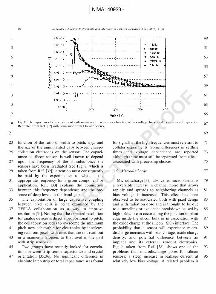
function of the ratio of width to pitch, w=p, andthe size of the unimplanted gaps between charge-collection electrodes on the sensor. The capaci-tance of silicon sensors is well known to dependupon the frequency of the stimulus once thesensors have been irradiated (see Fig. 8, which istaken from Ref. [32]); attention must consequentlybe paid by the experimenter to what is theappropriate frequency for a given component orapplication. Ref. [33] explains the connectionbetween this frequency dependence and the pre-sence of deep levels in the band gap.
The exploitation of large capacitive couplingbetween pixel cells is being examined by theTESLA collaboration as a way to improveresolution [34]. Noting that the expected resolutionfor analog devices is directly proportional to pitch,the collaboration seeks to overcome the minimumpitch now achievable for electronics by interleav-ing read out pixels with ones that are not read outin a manner analogous to that used in the pastwith strip sensors.
Two groups have recently looked for correla-tions between strip sensor capacitance and crystalorientation [35,36]. No significant difference inabsolute inter-strip or total capacitance was found
for signals at the high frequencies most relevant tocollider experiments. Some differences in settlingtimes and voltage dependence are reportedalthough these must still be separated from effectsassociated with processing choices.
3.5. Microdischarge
Microdischarge [37], also called microplasma, isa reversible increase in channel noise that growsrapidly and spreads to neighboring channels asbias voltage is increased. This effect has beenobserved to be associated both with pixel designand with radiation dose and is thought to be dueto a tunnelling or avalanche breakdown caused byhigh fields. It can occur along the junction implantedge inside the silicon bulk or in association withthe oxide charge at the silicon2SiO2 interface. Theprobability that a sensor will experience micro-discharge increases with bias voltage, oxide chargedensity, and potential difference between animplant and its external readout electronics.Fig. 9, taken from Ref. [38], shows one of theproblems that microdischarge poses for siliconsensors: a steep increase in leakage current atrelatively low bias voltage. A related problem is
1
3
5
7
9
11
13
15
17
19
21
23
25
27
29
31
33
35
37
39
41
43
45
47
49
51
53
55
57
59
61
63
65
67
69
71
73
75
77
79
81
83
85
87
89
91
93
95
Fig. 8. The capacitance between strips of a silicon microstrip sensor, as a function of bias voltage, for several measurement frequencies.
Reprinted from Ref. [32] with permission from Elsevier Science.
S. Seidel / Nuclear Instruments and Methods in Physics Research A 0 (2001) 1–3010
NIMA :40923 -

UNCORRECTED PROOF
noise amplitude, which, during microdischarge,increases with bias voltage as well. As thedominant cause of microdischarge is thought tobe a MOS effect associated with the implant andits conductive pad, the problem can be reduced ifthe implant is designed to extend at least 2 mmbeyond its conductor in all directions. Additionaloptions for reducing microdischarge are discussedin Refs. [38,39].
3.6. Signal and noise
The signal production by a semiconductor isassociated with ionization of the material bythrough-going charged particles. A review of thesubject, including corrections for statistical fluc-tuations, may be found in Ref. [40]. Fig. 10 showsthe rate of energy loss, dE=dx; in silicon, as afunction of the kinetic energy of a through-goingpion. In semiconductors, only part of the energylost by the particle subsequently creates electron–hole pairs, as phonon production may not beneglected. The average energy necessary to create apair in silicon is 3:6 eV; as a minimum ionizingparticle loses 1:66 MeV=g=cm2 in silicon, itsaverage energy loss along the h1 1 1i orientationof the lattice is 390 eV=mm. This translates toproduction of 108 pairs=mm or 3:2� 104 pairsalong a 300 mm track. There is no multiplication ofcharge in a silicon sensor.
The noise of a silicon detector assembly istypically dominated by the electronics contribu-tion rather than the sensor. Refs. [41,42] reviewissues associated with the electronics. To minimizethe sensor noise, one minimizes the leakage current(hence shot noise) and the capacitive load on theamplifier (see Section 3.4 above). Leakage currentis minimized in semiconductors with large bandgaps and few mid-gap (defect) states. As will bedescribed further in Section 4.1.1, the leakagecurrent may be further suppressed by operation ofthe sensor in a low-temperature environment.
It is apparent that both the signal and the noiseperformance of a sensor are directly related todefect density through trapping and generation. Itis because detector grade Group IV semiconduc-tors such as Ge and Si have defect densities thatare orders of magnitude lower than typicalcompound semiconductors that they are fre-quently chosen as substrates for devices requiringgood signal-to-noise ratio.
Radiation-induced lattice defects have beenshown to act as trap sites that lead to the loss ofup to 15% [43] of the signal in silicon strip sensorsafter fluences comparable to that received duringan LHC lifetime (2� 1014 p=cm2) and collectiontimes appropriate to LHC electronics (see Fig. 11).Fig. 12 shows trapping probabilities measuredseparately for electrons and holes in highlyirradiated silicon diodes. As irradiation proceeds,the electron signal is found to degrade faster than
1
3
5
7
9
11
13
15
17
19
21
23
25
27
29
31
33
35
37
39
41
43
45
47
49
51
53
55
57
59
61
63
65
67
69
71
73
75
77
79
81
83
85
87
89
91
93
95
Fig. 9. Microdischarge in a silicon sensor, as indicated by the
steep increase of total leakage current beyond 150 V. Reprinted
from Ref. [38] with permission from Elsevier Science.
Fig. 10. The rate of energy loss due to ionization, as a function
of kinetic energy of a charged pion traversing silicon with (solid
line) and without (dotted line) density and shell corrections.
Reprinted from Ref. [2] with permission.
S. Seidel / Nuclear Instruments and Methods in Physics Research A 0 (2001) 1–30 11
NIMA :40923 -

UNCORRECTED PROOF
the hole signal [44]. The charge collection efficiencyis independent of annealing time [45]. For 300 mmthick sensors irradiated with 24 GeV=c protons toa fluence of 1014 cm�2, a charge collectionefficiency of 90% was maintained with 160 V biasvoltage and collection time 20 ns. Those irradiatedwith 300 MeV=c protons to a fluence of 6� 1014
cm�2 maintained a 40% efficiency [46]. Thepresence of trap sites also changes the shape ofthe electric field distribution in the sensor andconsequently alters somewhat the shape of signalsto be read out.
3.7. Bulk-type inversion
As was mentioned in Section 3.1 and illustratedin Fig. 5, at a fluence of about 1012hni cm�2, thesubstrate of an initially n-type sensor begins tooperate as p-type; this is known as type inversion.An early hypothesis about the process was thatthe functional form of the effective dopant concen-tration, Neff , reflected donor removal (by theattachment of radiation-induced vacancies tophosphorus atoms) and shallow acceptor creation[47]. However, subsequent DLTS analysis hasindicated that considerably less phosphorus re-moval occurs than is required, and furthermore,no candidate acceptor state has yet been identified.
A new hypothesis has consequently been proposedthat the introduction of deep level acceptor statescauses n-type silicon to become effectively p-typewhen placed under bias [48].
1
3
5
7
9
11
13
15
17
19
21
23
25
27
29
31
33
35
37
39
41
43
45
47
49
51
53
55
57
59
61
63
65
67
69
71
73
75
77
79
81
83
85
87
89
91
93
95
Fig. 11. The measured charge collection efficiency of silicon
detectors as a function of bias voltage, for two levels of fluence
received. Reprinted from Ref. [43] with permission from
Elsevier Science.
Fig. 12. The trapping probability at two bias voltages for
irradiated silicon diodes, measured as a function of fluence for
(a) electrons and (b) holes. The dotted lines show the �1scontours of a fit to a linear relation between trapping
probability and fluence. Reprinted from Ref. [44] with
permission from Elsevier Science.
S. Seidel / Nuclear Instruments and Methods in Physics Research A 0 (2001) 1–3012
NIMA :40923 -

UNCORRECTED PROOF
Inversion manifests itself as an abrupt move-ment of the main junction from the p-side of thesensor to the n-side. Figs. 13 and 14, taken fromRef. [49], are direct evidence of this effect. On eachof them, the vertical axis shows the measuredpulseheight induced by an infrared LED directedat the segmented (p) and the back (n) sides of somestrip sensors fabricated on n-type substrate. Thehorizontal axis indicates bias voltage. The formerfigure concerns the sensors prior to irradiation; thelatter, after type inversion. One sees that prior toinversion, the signal may be read from the p-side at
low voltage, indicating that the junction is there,while the n-side signal does not develop until thevoltage is high enough to cause the depletionregion to extend to the back side. After inversion,the junction has moved to the n-side, and thesituation is reversed: the n-side signal is present atlow bias voltages, while the p-side signal appearsonly after full depletion. Inversion is not aproblem for the operation of the sensor as longas the design anticipates it. Design features thatare typically required for post-inversion n-sideoperation (for example channel isolation implantsand guard rings) are described in the sectionsbelow.
Several investigators have reported a relatedphenomenon: the development of a second junc-tion which appears on the p-side after inversion.The second junction, which has been observeddirectly [50,51] and reproduced in simulation [52],is associated with an n-type inversion layer ofthickness approximately 15 mm in the effectively p-type bulk. Ref. [52] points out that if more thanone defect type is present (for example, a dominantacceptor level and an additional donor level),trapped charge is not distributed uniformly acrossthe bulk: ‘‘[h]oles. . . are more efficiently trappedclose to the pþ junction side: such a region istherefore less inverted than the deeper bulk. . . .Therefore, within a certain range of fluences, adepletion layer can simultaneously originate fromdoping discontinuities at both ends of thedetector’’. Ref. [53] links the junction to a specificdonor-like level below mid-gap and an acceptor-like one above. Fig. 15 is a measurement of TCTcurrent in which the double-peaked structureindicates the presence of both junctions.
4. Techniques for increasing the radiation
robustness of proven sensor designs
4.1. Operating temperature minimization
4.1.1. Suppression of annealingSection 2.4.1 mentioned that radiation damage
manifests itself both in increased leakage currentand in a change to the effective dopant concentra-tion. The leakage current increase can be con-
1
3
5
7
9
11
13
15
17
19
21
23
25
27
29
31
33
35
37
39
41
43
45
47
49
51
53
55
57
59
61
63
65
67
69
71
73
75
77
79
81
83
85
87
89
91
93
95
Fig. 13. Pulseheights as a function of bias voltage for an
unirradiated silicon detector with an LED shining on the strip
and on the back side. The vertical scale is arbitrary and the
pulseheights are not normalized. Reprinted from Ref. [49] with
permission from Elsevier Science.
Fig. 14. Pulseheights as a function of bias voltage for a silicon
detector after type inversion, for an LED shining on the strip
and on the back side. The fluence received was 3� 1013 cm�2.
Reprinted from Ref. [49] with permission from Elsevier Science.
S. Seidel / Nuclear Instruments and Methods in Physics Research A 0 (2001) 1–30 13
NIMA :40923 -
UNCORRECTED PROOF
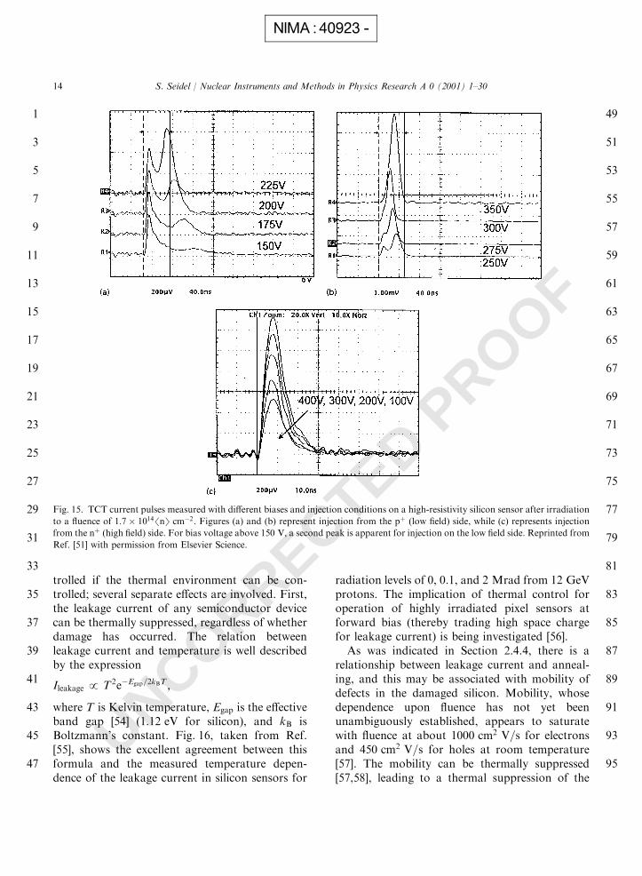
trolled if the thermal environment can be con-trolled; several separate effects are involved. First,the leakage current of any semiconductor devicecan be thermally suppressed, regardless of whetherdamage has occurred. The relation betweenleakage current and temperature is well describedby the expression
Ileakage / T2e�Egap=2kBT ;
where T is Kelvin temperature, Egap is the effectiveband gap [54] (1:12 eV for silicon), and kB isBoltzmann’s constant. Fig. 16, taken from Ref.[55], shows the excellent agreement between thisformula and the measured temperature depen-dence of the leakage current in silicon sensors for
radiation levels of 0, 0.1, and 2 Mrad from 12 GeVprotons. The implication of thermal control foroperation of highly irradiated pixel sensors atforward bias (thereby trading high space chargefor leakage current) is being investigated [56].
As was indicated in Section 2.4.4, there is arelationship between leakage current and anneal-ing, and this may be associated with mobility ofdefects in the damaged silicon. Mobility, whosedependence upon fluence has not yet beenunambiguously established, appears to saturatewith fluence at about 1000 cm2 V=s for electronsand 450 cm2 V=s for holes at room temperature[57]. The mobility can be thermally suppressed[57,58], leading to a thermal suppression of the
1
3
5
7
9
11
13
15
17
19
21
23
25
27
29
31
33
35
37
39
41
43
45
47
49
51
53
55
57
59
61
63
65
67
69
71
73
75
77
79
81
83
85
87
89
91
93
95
Fig. 15. TCT current pulses measured with different biases and injection conditions on a high-resistivity silicon sensor after irradiation
to a fluence of 1:7� 1014hni cm�2. Figures (a) and (b) represent injection from the pþ (low field) side, while (c) represents injection
from the nþ (high field) side. For bias voltage above 150 V, a second peak is apparent for injection on the low field side. Reprinted from
Ref. [51] with permission from Elsevier Science.
S. Seidel / Nuclear Instruments and Methods in Physics Research A 0 (2001) 1–3014
NIMA :40923 -

UNCORRECTED PROOF
component of leakage current associated withdamage. The effective dopant concentration Neff
of an irradiated silicon sensor is given in Section2.4.3 by the sum of three terms, each of whichcorresponds to a type of annealing with itsown time constant. Because of the temperaturedependence of the annealing coefficients, a 300 mmthick detector-grade sensor that has received a1014hni cm�2 fluence can have a depletion voltageanywhere in the range 200–800 V, depending upon
the temperature of its post-irradiation environ-ment. The annealing coefficients with finite timeconstants, Na and NY, can be completely sup-pressed by reduction of the sensor temperature, afact demonstrated in Fig. 17 (taken from Ref.[59]). To minimize the sensor’s depletion voltage,the sensor should be operated at a temperaturehigh enough to activate beneficial annealing butlow enough to suppress reverse annealing. Thetemperature range �10–08C is appropriate toachieve this for LHC lifetimes and fluences.
4.1.2. The ‘‘Lazarus Effect’’The ability of a highly irradiated silicon sensor
to recover its essential pre-irradiation operatingcharacteristics when run at cryogenic tempera-tures has been demonstrated [60]. A 300 mmthick silicon strip sensor was irradiated to2:23� 1015hni cm�2. When biased to 250 V, itshowed no signal at 195 K. With its temperaturelowered to 77 K, it recovered a fast, 13000e�
signal (see Fig. 18). No further improvement wasobserved when the temperature was lowered to4:2 K. The device was stored at room temperatureand only operated cold; this effect is different fromthe one that suppresses annealing. The model thathas been offered for this ‘‘Lazarus Effect’’ is basedon the fact that at cryogenic temperatures, the lowthermal energy of the silicon lattice reduces thedetrapping rate of carriers, so a large fraction of
1
3
5
7
9
11
13
15
17
19
21
23
25
27
29
31
33
35
37
39
41
43
45
47
49
51
53
55
57
59
61
63
65
67
69
71
73
75
77
79
81
83
85
87
89
91
93
95
Fig. 16. The temperature dependence of leakage current, for
devices that received 0, 0.1, and 2 Mrad. The solid lines are fits
to the formula given in the text. Reprinted from Ref. [55] with
permission from Elsevier Science.
Fig. 17. Depletion voltage as a function of time for silicon sensors annealed at the indicated temperatures. All of the devices received a
fluence close to 5� 1013 cm�2. Reprinted from Ref. [59] with permission from Elsevier Science.
S. Seidel / Nuclear Instruments and Methods in Physics Research A 0 (2001) 1–30 15
NIMA :40923 -
UNCORRECTED PROOF
the deep levels is constantly filled and hencedeactivated. A small inefficiency which persists inthe sensor at low bias voltages even at 4:2 K,where defects are expected to be frozen out, maybe explained by the presence of the hexavacancycomplex, V6 [61]. The charge collection efficiency ismaximized at 130 K and shows some timedependence [62].
4.2. Control of the accumulation layer
In Section 3.3, it was mentioned that asradiation fluence increases, bound positive surfacecharge develops at the silicon–oxide interface, andthat this fixed charge attracts electrons that canultimately short the n-implants. The p-stop [63]and p-spray [64] techniques have been developedto maintain implant isolation.
p-stops are implanted pþ channels betweenneighboring n-implants. They have been imple-mented in some pixel designs after successfulapplication in microstrip sensors. Fig. 19, fromRef. [65], illustrates some of the patterns (ordin-ary, common, atoll, and combined) that have beenexamined. Optimization of a p-stop designrequires consideration of the effect of thesep-implants upon the pixel charge collection effi-ciency and capacitance as well as on the n-implantisolation. Fig. 20, also from Ref. [65], shows thatpixels utilizing the ordinary p-stop typically showthe highest charge collection efficiency, followedby those with the combined design. The reduced
1
3
5
7
9
11
13
15
17
19
21
23
25
27
29
31
33
35
37
39
41
43
45
47
49
51
53
55
57
59
61
63
65
67
69
71
73
75
77
79
81
83
85
87
89
91
93
95
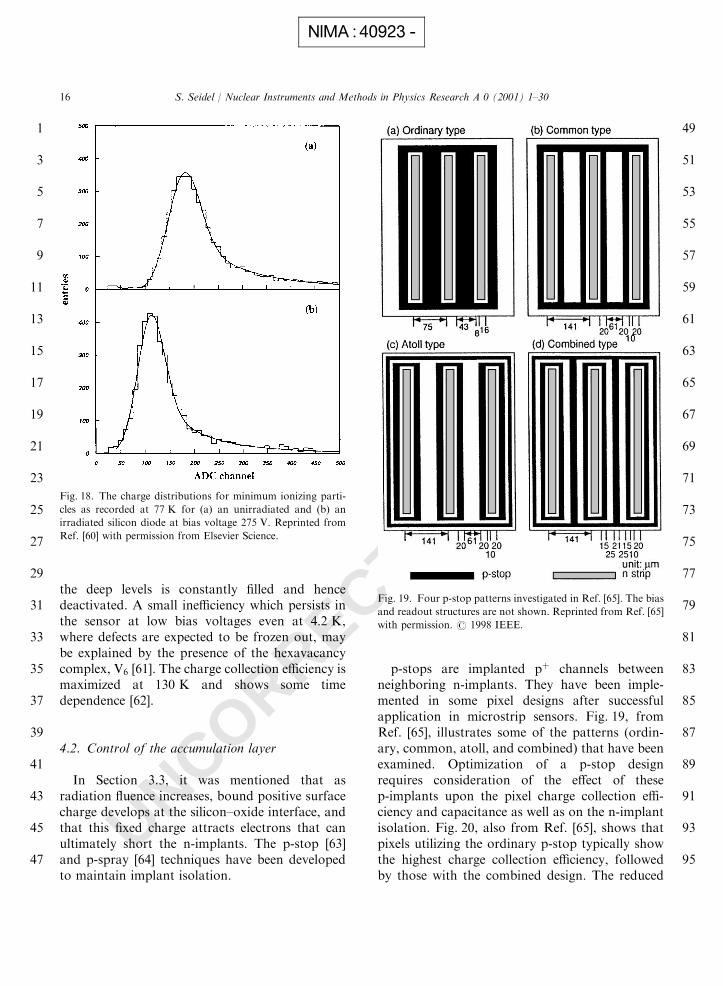
Fig. 18. The charge distributions for minimum ionizing parti-
cles as recorded at 77 K for (a) an unirradiated and (b) an
irradiated silicon diode at bias voltage 275 V. Reprinted from
Ref. [60] with permission from Elsevier Science.
Fig. 19. Four p-stop patterns investigated in Ref. [65]. The bias
and readout structures are not shown. Reprinted from Ref. [65]
with permission. # 1998 IEEE.
S. Seidel / Nuclear Instruments and Methods in Physics Research A 0 (2001) 1–3016
NIMA :40923 -

UNCORRECTED PROOF
efficiency of the atoll design is thought to followfrom the fact that the atoll p-stop does notsegment all of the accumulation layer. Chargedeposited between atolls can be coupled away bythe accumulation layer, which is conductive, andthis leads to inefficiency. The combined design, onthe other hand, has the lowest capacitance (hence,noise) [29,63]. It is clear that decisions aboutp-stop design must be made in the context of thefull detector design including information aboutother contributors to capacitance (for example, inthe electronics).
A p-spray layer is a shallow p-type implant thatis applied across the full wafer without mask priorto any other processing. The dopant concentrationof the implant is matched to the well-known valueat which surface charge saturates, 3� 1012 cm�2.
Subsequent n-implantation then over-compensatesthe p-spray layer wherever needed. p-spray devicesuse the growth of the accumulation layer to theiradvantage: the accumulation layer compensatesthe dopant acceptors, so that as radiation pro-ceeds, the p-spray layer becomes increasinglycloser to intrinsic. The lateral electrical fieldbetween implants consequently decreases withfluence, increasing the breakdown voltage.Fig. 21, from Ref. [64], shows the results of atechnology simulation of a p-stop and a p-spraydevice for various levels of oxide charge density(hence, ionizing radiation). One sees that in thecase of the p-spray device, but not in the case ofthe p-stop, the electric field magnitude decreases(and hence the breakdown voltage increases) withfluence. This improvement of radiation hardness
1
3
5
7
9
11
13
15
17
19
21
23
25
27
29
31
33
35
37
39
41
43
45
47
49
51
53
55
57
59
61
63
65
67
69
71
73
75
77
79
81
83
85
87
89
91
93
95
Fig. 20. Pulseheight in adjacent strips as a function of laser position for silicon strip sensors with the p-stop patterns shown in Fig. 19.
The sum of the signals on the two strips is also plotted. The bias voltage was 80 V. Reprinted from Ref. [65] with permission. # 1998
IEEE.
S. Seidel / Nuclear Instruments and Methods in Physics Research A 0 (2001) 1–30 17
NIMA :40923 -

UNCORRECTED PROOF
with irradiation has been demonstrated with theATLAS prototypes [66].
Control of the accumulation layer is also ageometrical issue. Studies of surface effects show aclear relationship between the generated surfacecurrent of irradiated pixels and the size of the gap
between implants [67]. Fig. 22 compares thecurrent after 11 kGy for pixels with large andsmall gaps. The exponential rise in leakage currentin the large gap devices is ascribed to theconfinement of accumulation layer electrons inthe gap as a consequence of the adjacent depletion
1
3
5
7
9
11
13
15
17
19
21
23
25
27
29
31
33
35
37
39
41
43
45
47
49
51
53
55
57
59
61
63
65
67
69
71
73
75
77
79
81
83
85
87
89
91
93
95
Fig. 21. Maximum electric field versus voltage VPþ between a p-doped isolation layer and an adjacent nþ strip, as predicted for
increasing oxide charge density Nox by a technology simulation. (a) represents p-stop isolation and (b), p-spray. The parameters of the
simulation may be found in Ref. [64], from which this figure is reprinted with permission from Elsevier Science.
S. Seidel / Nuclear Instruments and Methods in Physics Research A 0 (2001) 1–3018
NIMA :40923 -

UNCORRECTED PROOF
zones coallescing before the flat-band voltage isreached. In addition to improving the radiationresistance of the sensor, p-spray has the benefitthat since no mask is required for its application,the cost of implant isolation is lowered, andneighboring n-type structures can be placed closer.
4.3. Control of electrical breakdown
Guard rings, typically implanted and metallizedstructures that surround the active areas of siliconsensors, serve two purposes. (1) As the depletionregion develops from the junction, it expandstoward the cut edge which, due to its mechanicaldamage, is conductive. The guard ring serves todrop the voltage from the interior of the sensorface to the cut edge in a controlled manner, so thatthe voltage gradient across the edge is zero. (2) Theaccumulation layer induced by the presence offixed charge at the oxide deforms the depletionregion, generating high field points at risk ofelectrical breakdown. The oxide layer is unstableand sensitive to changes in the environment;consequently, the behavior of the accumulationlayer is variable. The guard ring serves to stabilizethe oxide and to shape the depletion region. Tomeet these requirements, typical guard ring struc-tures include metal lines atop the oxide plus one ormore ring-shaped p–n junctions that surround thediode array but are not contacted or biaseddirectly.
Fig. 23, from Ref. [68], is an example guard ringlayout. (A variety of designs have been proven to
be successful; this example is selected merely toillustrate several concepts.) The rings in this designare a serial connection of p-channel MOSFETs, inwhich the gate only covers half of the distancebetween the drain and source of the sensor. Thegates are connected to the sources rather than thedrains. The guard ring is operated by biasing then-side and grounding the active area and innerguard. As bias voltage rises, the depletion regionexpands. When it contacts, or ‘‘punches throughto’’ the first floating ring, that ring charges up.Increasing the voltage further biases all of the ringssequentially. Each ring’s potential depends uponthe bulk dopant concentration and oxide charge(hence on the fluence) as well as on the separationbetween rings. When charged, the rings distributethe diode’s field beyond the diode’s perimeter, thusreducing rV at every surface point. Fig. 24, fromRef. [69], represents the electrostatic potential at
1
3
5
7
9
11
13
15
17
19
21
23
25
27
29
31
33
35
37
39
41
43
45
47
49
51
53
55
57
59
61
63
65
67
69
71
73
75
77
79
81
83
85
87
89
91
93
95
Fig. 22. Measurements of current versus voltage of pixels with gaps of size (a) 100 mm and (b) 10 mm between their implants, after
receipt of 11 kGy irradiation. Reprinted from Ref. [67] with permission from the Societ"a Italiana di Fisica and the original authors.
Fig. 23. An example guard ring layout with non-overlapping
gate. Reprinted from Ref. [68] with permission from Elsevier
Science.
S. Seidel / Nuclear Instruments and Methods in Physics Research A 0 (2001) 1–30 19
NIMA :40923 -

UNCORRECTED PROOF
the sensor surface, as a function of distance fromthe sensor center, for measurements and simula-tions of a guard ring structure with a variety ofoptions in surface charge density. One clearly seesthat the multi-ring structure steps the voltage by acontrolled amount at the location of each ring.
In a particular set of related simulations anddesigns, the breakdown voltage associated with theguard ring structure was found to increase withdistance of the outermost guard to the scribelineup to a distance of 150 mm, and then saturate [70].The breakdown voltage is maximized for thenarrowest achievable inter-ring gaps. The inner-most guard must be connected to guarantee thatthe field is correctly shaped (see Fig. 2) [12]. It isworth emphasizing that n-side guard rings areinactive prior to inversion, and p-side rings, after.Guard ring designs that tolerate 500 V after afluence of 1014hni cm�2 [25] and those thattolerate 900–1000 V before [70] have been demon-strated.
A study of pþ-on-n devices has also examinedthe use of an nþ implanted region along the edgeto inhibit avalanche breakdown [71]. It concludedthat the nþ implant should be no closer than 150mm to the pþ and that the pþ implant should beno closer to the edge than 400 mm. Drive indiffusion steps lead in general to smoother junc-tions and lower electric fields [72].
4.4. Crystal orientation
It has generally been supposed that the h1 0 0icrystal orientation is more radiation hard than theh1 1 1i one because its oxide charge density islower. The h1 1 1i has nonetheless traditionallybeen used for silicon sensors because in surfacebarrier detectors and p–n diodes, the higher oxidecharge inhibits breakdown. Furthermore, theh1 1 1i orientation reduces signal dispersion dueto channeling in spectrometry.
1
3
5
7
9
11
13
15
17
19
21
23
25
27
29
31
33
35
37
39
41
43
45
47
49
51
53
55
57
59
61
63
65
67
69
71
73
75
77
79
81
83
85
87
89
91
93
95
3————————————————————Fig. 24. The measured and simulated potential distributions
along the surface of a particular multi-guard ring structure. The
three plots show the results for different oxide charge densities
and substrate doping concentrations. The details of the design
may be found in Ref. [69], from which this figure is reprinted
with permission from Elsevier Science.
S. Seidel / Nuclear Instruments and Methods in Physics Research A 0 (2001) 1–3020
NIMA :40923 -

UNCORRECTED PROOF
It has been reported [73] that sensors fabricatedfrom epitaxial silicon with the h1 1 1i crystalorientation are more radiation hard than are thosewith h1 0 0i. The devices about which the reportwas made have resistivity 630 O=cm, considerablyless than the resistivity traditionally used fordetectors. While it is reasonable to expect thatsilicon wafers with different growing conditions,including orientation, may have different re-sponses to radiation, the full connection betweenradiation hardness, crystal orientation, and lowresistivity of these devices has, however, not yetbeen fully sorted out.
4.5. The p-type substrate option
Most silicon sensors fabricated up to this timehave used n-type substrates. While p- and n-typesilicon substrates have rather similar radiationdamage constants [74,75], n-type material has theadvantage that its majority carriers, the electrons,have three times higher mobility than holes [54];the depletion voltage is correspondingly lower.The principal benefit of beginning with p-typesubstrate is the fact that inversion does not occur.The junction then remains on the n-side of thesensor throughout its lifetime, simplifying qualityassurance of the devices and some aspects of thedesign.
5. Initiatives to improve radiation hardness for
future detectors
5.1. Introduction
At present the majority of silicon sensors used inparticle physics applications have resulted fromplanar processing of high-resistivity n-type floatzone silicon wafers. While the vast majority haveutilized 4-in. wafers, no difference has beenobserved in those produced on wafers of diameter6 in. [76]. Several interesting routes are beingexplored to increase the radiation hardness ofdetector-quality devices: (1) reduced substrateresistivity, (2) epitaxial or Czochralski substrates,(3) alternatives to planar processing, (4) oxygena-
tion of the silicon, and (5) other semiconductors.This section reports on the status of each of these.
5.2. Wafer fabrication and processing options
5.2.1. Substrate resistivityThe usual classification system identifies detec-
tors of bulk resistivity r around 5–10 kO=cm ashigh resistivity, those with r around 1 kO=cm,medium resistivity, and those with r5500 O=cm,low resistivity. While lower resistivity silicon has ahigher pre-irradiation depletion voltage than doeshigh, it also has a higher inversion fluence.Inversion fluences Finversion for the resistivity range1:54r420 kO=cm have been shown [77] to bewell described by the equation, Finversion ¼ 18�Neff0: A low starting resistivity reflects a highdensity of built-in donor defects.
The use of low-resistivity silicon merits explora-tion for several reasons [78,79] including the lowersubstrate cost and the fact that, for applications inwhich inversion is guaranteed not to occur, single-sided wafer processing, with its associated simpli-fications and cost reduction, may be used. Fullactivation, or punchthrough, of all rings in amulti-ring guard structure on such a device isachieved with lower voltage. Lastly, whereasleakage current grows with fluence, depletionvoltage decreases with it prior to inversion;consequently power dissipation is balancedthroughout the lifetime of a sensor that will beutilized only prior to inversion.
Several low-resistivity sensors have been fabri-cated, irradiated, and operated in exploratorystudies. Fig. 25 shows the effective dopant densityof one such 130 O=cm demonstration sensor as afunction of fluence F. One sees that the device isuninverted up to F ¼ 9� 1014hni cm�2. Detectorquality sensors are not yet available with this lowresistivity.
Unfortunately, no absolute advantage in deple-tion voltage can be gained from low-resistivitysilicon that has the standard amount of absorbedoxygen: the resistivity must be achieved with highlyoxygenated wafers (see Section 5.2.3 below).Extrapolations from existing data (see Fig. 26)predict that after one LHC lifetime (10 years),
1
3
5
7
9
11
13
15
17
19
21
23
25
27
29
31
33
35
37
39
41
43
45
47
49
51
53
55
57
59
61
63
65
67
69
71
73
75
77
79
81
83
85
87
89
91
93
95
S. Seidel / Nuclear Instruments and Methods in Physics Research A 0 (2001) 1–30 21
NIMA :40923 -

UNCORRECTED PROOF
standard silicon wafers of all resistivities willrequire the same depletion voltage [46].
5.2.2. Epitaxial and Czochralski siliconDuring production by the float zone method, a
polycrystalline ingot is suspended in vacuum or aninert gas and heated to melting in a narrow regionalong its length. The position of the interface zonebetween the solid and liquid regions is then slowlymoved through the material. Because the solubi-lities of some impurities are different in solid and
liquid silicon, sweeping the liquid zone through thelength of the ingot transports the impurities to theend of the ingot, which may be excised. Repeatedsweeps leave a highly purified crystal.
The Czochralski method also uses the fact that amoving liquid zone purifies the silicon, but beginsinstead with a seed crystal lowered into moltensilicon. As the seed is raised and rotated, orientedcrystals grow upon it. Czochralski-grown ingotshave a higher oxygen concentration than do floatzone, because the molten silicon is in contact withthe SiO2 crucible.
In the epitaxial process, one begins with asubstrate (which may be silicon or a material witha similar lattice structure) and exposes it to anenvironment of free atoms. These deposit on it,preserving the substrate crystal’s aspect. Thedeposition process for silicon is most commonlychemical vapor deposition, or CVD. The growthrate for silicon is normally between 0.5 and 1:0 mmper minute.
Epitaxial silicon is known to have more as-grown defects, more crystal mismatch, and conse-quently larger strain fields and internal stress thanfloat zone silicon [80]. Prior to irradiation, typicalsamples contain high (52� 1012 cm�3) deep levelconcentrations. It is hypothesized that as-growndeep levels can provide a sink for radiation-induced defects; recently, research has been under-taken to take advantage of this phenomenon [81].
Deep Level Transient Spectroscopy has beenapplied to samples of non-oxygenated epitaxialsilicon to identify the deep levels present. Themiddle element of Fig. 27 shows the spectrum foran unirradiated epitaxial silicon sample. Thissample was irradiated to a fluence of 1:5� 1011
cm�2 with 24 GeV=c protons, then re-examined byDLTS. The spectrum of the irradiated device isshown in the upper element of Fig. 27, and it isunchanged}no new levels have developed. Thelower element of the same figure shows thecontrasting spectrum for float zone silicon thatreceived similar treatment.
The ability of the as-grown defects to act assinks is limited by their density. For the samplesmentioned above, saturation was observed after afluence of 6� 1013 protons cm�2, at which pointthe DLTS trap spectrum for the sample was
1
3
5
7
9
11
13
15
17
19
21
23
25
27
29
31
33
35
37
39
41
43
45
47
49
51
53
55
57
59
61
63
65
67
69
71
73
75
77
79
81
83
85
87
89
91
93
95
Fig. 26. The calculated depletion voltage as a function of LHC
operational years for the first layer of the ATLAS SCT barrel
(radius 30 cm; z ¼ 0 cm, fluence 1:75� 1013 cm�2 per year at
full luminosity). Reprinted from Ref. [46] with permission from
Elsevier Science.
Fig. 25. The effective dopant density as a function of fluence
for a demonstration low resistivity ð130 O cmÞ pþ=n=nþ silicon
sensor. Reprinted from Ref. [79] with permission from Elsevier
Science.
S. Seidel / Nuclear Instruments and Methods in Physics Research A 0 (2001) 1–3022
NIMA :40923 -

UNCORRECTED PROOF
similar to that of float zone silicon. Increasing theas-grown defect density of epitaxial silicon requiresincreasing the growing time for the ingot. Theconcentration of its defects increases non-linearlywith thickness [81].
In other respects epitaxial and float zonematerial have comparable qualities. Their reverseannealing constants are similar}one can see thisin Fig. 28, which shows similar development of theeffective dopant concentration, Neff , for controlfloat zone samples and for several epitaxialsamples. Epitaxial and float zone samples ofsimilar initial resistivities have nearly the sameinversion fluence [73].
Czochralski silicon can achieve oxygen concen-trations up to 1018 cm�3. While this high oxygena-tion may eventually prove valuable for radiationhardness (see Section 5.2.3), Czochralski silicon is
1
3
5
7
9
11
13
15
17
19
21
23
25
27
29
31
33
35
37
39
41
43
45
47
49
51
53
55
57
59
61
63
65
67
69
71
73
75
77
79
81
83
85
87
89
91
93
95
Fig. 27. Deep Level Transient Spectroscopy spectra of n-type
silicon sensors for the cases in which (upper) the material is
epitaxial and the fluence is 1:5� 1011 p=cm2; (middle) the
epitaxial material is unirradiated; and (lower) the similarly
irradiated material is standard bulk silicon. Reprinted from
Ref. [81] with permission. # 1998 IEEE.
Fig. 28. The reverse annealing behavior for epitaxial silicon
sensors and control samples, as indicated by depletion voltage
and effective dopant concentration versus elevated temperature
ð808CÞ annealing (ETA) time. Reprinted from Ref. [81] with
permission. # 1998 IEEE.
S. Seidel / Nuclear Instruments and Methods in Physics Research A 0 (2001) 1–30 23
NIMA :40923 -

UNCORRECTED PROOF
not yet available as detector quality wafers.Czochralski material has been used as a substratefor epitaxial deposition [82] with the intent that itsoxygen diffuse into the epitaxial material.
5.2.3. Oxygenation of the substrateIt has been hoped for some time that one could
improve the radiation tolerance of silicon by defectengineering, which is the deliberate addition ofimpurities to the silicon in order to form electri-cally active defects and thereby control themacroscopic behavior of the material. Significanteffort has been applied to studies with oxygen andcarbon.
Results available in late 1998 first showed thatwhen oxygen is introduced to the silicon waferabove a specific threshold concentration, thesilicon is found to be up to 3 times more radiationhard against charged hadrons [83]. The oxygenmay be introduced to the silicon by jet injection atthe ingot stage or by diffusion at high temperatureafter oxidation of the wafers. The exact value ofthe threshold, and optimized parameters for theoxygen’s introduction, are still under investigation,but there are indications that a diffusion of 16 h at11508C, such that ½O� ¼ 1:5� 1017 cm�3 in a 300
mm wafer, may be adequate.1 Fig. 29 shows thereduction in full depletion voltage (equivalently,Neff ) as a function of proton fluence, observed foroxygenated wafers.
This discovery is accompanied by two interest-ing effects that have not yet been fully explained.The first is the fact that the improved radiationresistance applies to charged particles but not toneutrons. This apparent violation of the NIELscaling hypothesis by the charged particles isreceiving considerable attention. It is noted thatmore point defects are produced by chargedparticle irradiation than by neutral. A secondunexpected consequence of oxygenation is itssuppression of reverse annealing. Rather thanremaining proportional to the fluence, as is thecase for standard silicon, the reverse annealingcomponent of the effective dopant concentrationin oxygenated wafers saturates above a fluenceof about 2� 1014hni cm�2, leading to a reductionof NY by about a factor of 2. The reverseannealing time constant is, furthermore,
1
3
5
7
9
11
13
15
17
19
21
23
25
27
29
31
33
35
37
39
41
43
45
47
49
51
53
55
57
59
61
63
65
67
69
71
73
75
77
79
81
83
85
87
89
91
93
95
Fig. 29. The effective space charge density and full depletion voltage as a function of proton fluence for standard, carbon enriched, and
three types of oxygen diffused silicon diodes. The oxygenated devices were produced with diffusion times of 24, 48, and 72 h at 11508C.Reprinted from Ref. [83] with permission from Elsevier Science.
1Typical high-grade, high-resistivity float zone silicon con-
tains oxygen at a concentration of about 1015 cm�3 without
special processing.
S. Seidel / Nuclear Instruments and Methods in Physics Research A 0 (2001) 1–3024
NIMA :40923 -

UNCORRECTED PROOF
enhanced and appears to depend upon the oxygenconcentration.
Several suggestions [84,85] have been offered toexplain the beneficial effect of the oxygen. Oneproposes that the defect responsible for theformation of negative space charge in the bulkunder bias may be the divacancy–oxygen complex,V2–O. Increasing the concentration enhances theformation of the vacancy–oxygen complex, V–O,and so suppresses V2–O. While correlationsbetween microscopic defects and macroscopicdamage parameters have been observed, the naivesuppression model does not adequately accountfor volume current increase due to hadronicradiation. It has been proposed [86] that chargeexchange between traps inside clusters may de-scribe a significant portion of the current genera-tion and space charge density associated withneutron irradiation.
The following facts have emerged about bene-ficial oxygenation. The oxygen must be substitu-tional; a silicon wafer prepared with aconcentration of 2� 1017 cm�3 interstitial oxygenatoms was shown to be no more radiation hardthan normal silicon [87]. Epitaxial wafers with anoxygen concentration of 5� 1017 cm�3 havedemonstrated an inversion fluence two timeshigher than standard float zone wafers of thesame initial resistivity [88]. Oxygen-rich Czochrals-ki wafers show half the generation rate for reverseannealing as do normal Czochralski wafers,although other annealing parameters such as aand gC are unchanged by oxygen [18].
Like oxygen, tin added to silicon has beenshown to act as a vacancy trap [89]; the implica-tions of this for radiation hardness are beingexplored [90]. Some investigators have alsopointed out the potential of nitrogen doping [46].Germanium introduced to silicon at concentrationof 1019 cm�3 has thus far not proved beneficial,possibly due to Ge-vacancy complex instability atroom temperature [90]. The introduction ofcarbon into the wafer causes sensors to degradewith irradiation.
5.2.4. Alternatives to planar processingPlanar technology, which was originally in-
vented for microelectronics processing, required
adaptation [91] for use in the production ofsilicon sensors but is now the usualprocedure. The planar process generally involvesphotolithographic structuring, chemical etching,doping, oxidation, deposition of insulating andconducting layers by chemical reaction,deposition of metals by evaporation orsputtering, thermal treatment, and passivation.A general discussion of the process may befound in Ref. [54]. An alternative process, knownas mesa, has been applied to the productionof pþ2n2nþ diodes. The mesa process involveshigh-temperature diffusion in a normalatmosphere of boron and phosphor to forma progressive junction and an ohmic contactdeep in the bulk. Mesa processing eliminatesthe oxidation and masking stages and producesdevices which, lacking guard rings yet havingjunctions that extend to the device edge, typicallyshow higher leakage currents. It was inventedfor single diode pads and is not available at thistime for multi-diode arrays. It has, however,produced devices with improved radiation toler-ance relative to that observed for comparableplanar devices. It is under study in the hope thatthe essential features that improve radiationhardness may be discovered and transferred toother technologies.
A 1998 study [92] showed that mesa silicon,prepared with or without oxygenation, suppressesproton-induced change in effective dopant con-centration by a factor of two relative to planarprocessed epitaxial or float zone material. Acomplementary study [93] using neutrons,however, showed no difference between mesa andplanar diode full depletion voltages after a fluenceof 5� 1013 cm�2. Oxygenated mesa diodesalso show a smaller change in leakage currentin response to proton irradiation than do oxyge-nated planar devices [92]. One group [94] hasreported an as-yet unexplained initial decrease inNeff in p-type mesa silicon for low proton fluences.A very large increase in the oxygen concentrationof silicon processed with mesa technology has beenobserved [73]; the relationship between the benefitsthat stem from this oxygenation and thoseassociated with oxygenation of planar devices isunder study.
1
3
5
7
9
11
13
15
17
19
21
23
25
27
29
31
33
35
37
39
41
43
45
47
49
51
53
55
57
59
61
63
65
67
69
71
73
75
77
79
81
83
85
87
89
91
93
95
S. Seidel / Nuclear Instruments and Methods in Physics Research A 0 (2001) 1–30 25
NIMA :40923 -

UNCORRECTED PROOF
5.3. Non-silicon substrates
Several initiatives are underway to identifysemiconductors that, like silicon, have relativelylarge band gaps and so are expected to beradiation hard. The majority of work in this areahas been applied to development of GaAs anddiamond. Ref. [95], and references therein, providea recent status report on GaAs. While it typicallyhas a leakage current 10 times that of comparablequality silicon, other properties [96] of GaAs haveattracted significant attention to it. These includethe fact that it has twice the density of silicon, fourtimes better radiation length, the same pairproduction energy, and a carrier mobility that is5 times greater than silicon’s: this would imply thata 150 mm GaAs sensor could collect the samecharge as a 300 mm silicon one. GaAs devices havebeen demonstrated to have signal-to-noise ratiosof at least 30, and charge collection efficienciesgreater than 95%, prior to irradiation. Fabricationby a non-standard technology has produced a‘‘compensated GaAs’’ with approximately equalconcentrations of donors and acceptors and apurity comparable to that obtainable with silicon.The high dopant concentration allows the sensorto collect charge without external bias. Unfortu-nately, GaAs has not proven to be as radiationhard as was initially hoped [97,98].
An excellent recent review of diamond detectorsappears in Ref. [99]. The band gap in diamond is5:5 eV, approximately five times larger thansilicon’s. Consequently bulk currents in diamondare negligible ð100 pA cm�2 for 500 mm thickdevices) and no depletion is necessary, so no diodestructure is required. This large band gap leads toextreme radiation hardness: diamond sensorsexposed to radiation showed no degradation afterphoton fluence up to 100 Mrad and a particlefluence up to 1013 cm�2 [100]. After a 300 MeV=cpion fluence of 1:1� 1015 cm�2, the most probablesignal decreased by less than 15%. Exposure to24:2 GeV=c protons produced a measurable effectonly after about 2� 1015 cm�2. At 0:75� 1015
1-MeVhni cm�2, the mean value of the signaldistribution decreased by about 15%, but the mostprobable value was unaffected [101]. Furthermore,diamond’s low dielectric constant of 5.6 leads to a
relatively low sensor capacitance at the input tothe read out electronics.
Diamond crystals generate 13,500 pairs along a300 mm track, about a factor of two fewer thansilicon. The important figure of merit for diamondis its charge collection distance (CCD), which isthe average distance an electron and hole separateunder the influence of the external electric fieldbefore they are trapped. CCD is related to chargecollection efficiency (CCE) through the equation,CCD ¼ CCE� thickness. Considerable effort hasbeen devoted to increasing charge collectiondistance in diamond during the past 10 years,and the improvement has been significant; atypical CCD is now approximately 250 mm.Charge collection distance improves by 50–100%with irradiation up to saturation at 10 krad,through a process called pumping. The model forthis proposes that charge traps are reversibly filledby radiation-induced defects, and hence deacti-vated. Fig. 30 shows the increase in CCD duringexposure to a 90Sr source. A diamond detector atthe LHC would remain pumped throughout its lifeand would survive for 10 years at 7:5 cm from theinteraction point.
A diamond strip sensor has been fabricated with50 mm pitch. When operated with an analogpreamplifier of shaping time 25 ns, it showedsignal-to-noise ratio of 7 and position resolutionof 18 mm. A 16� 16 array of 150 mm square pixels
1
3
5
7
9
11
13
15
17
19
21
23
25
27
29
31
33
35
37
39
41
43
45
47
49
51
53
55
57
59
61
63
65
67
69
71
73
75
77
79
81
83
85
87
89
91
93
95Fig. 30. Mean charge collection distance as a function of time
during exposure of a diamond detector to a 90Sr source.
Reprinted from Ref. [99] with permission from Elsevier Science.
S. Seidel / Nuclear Instruments and Methods in Physics Research A 0 (2001) 1–3026
NIMA :40923 -
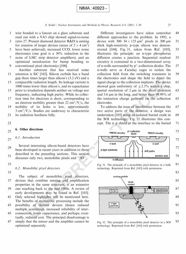
UNCORRECTED PROOF
wire bonded to a fanout on a glass substrate andread out with a VA3 chip showed signal-to-noiseratio 27. Present diamond detector R&D is aimingfor creation of larger devices (areas of 2� 4 cm2)have been achieved), increased CCD, lower noiseelectronics (one goal is a 30% reduction in thenoise of LHC strip detector amplifiers), and anoptimized metalization for bump bonding toconventional pixel electronics [100].
Another substrate that has received someattention is SiC [102]. Silicon carbide has a bandgap three times larger than silicon’s (3:2 eV) and acomparable radiation length. Its leakage current is1000 times lower than silicon’s, and its capacitanceprior to irradiation depends neither on voltage norfrequency, indicating high purity. While its collec-tion time for electrons is short, corresponding toan electron mobility greater than 22 cm2=V=s, themobility of its holes is low, approximately3 cm2=V=s. Studies are underway to characterizeits radiation hardness fully.
6. Other directions
6.1. Introduction
Several interesting silicon-based detectors havebeen developed in recent years in addition to thosedescribed in the preceding sections. This sectiondiscusses only two, monolithic pixels and ‘‘3D’’.
6.2. Monolithic pixel detectors
The subject of monolithic pixel detectors,devices that combine sensing and amplificationproperties in the same structure, is an extensiveone reaching back to the mid-1980s. A review ofearly developments may be found in Ref. [103].Only selected highlights will be mentioned here.The benefits of monolithic processing include thepossibility of thinner devices (hence reducedmultiple scattering), increased reliability of inter-connection, lower capacitance, and perhaps, even-tually, reduced cost. The principal disadvantage issimply that the sensor and the amplifier cannot beoptimized separately.
Different investigators have taken somewhatdifferent approaches to the problem. In 1992, adevice with 300 34� 125 mm2 pixels in 300 mmthick high-resistivity p-type silicon was demon-strated [104]. Fig. 31, taken from Ref. [105],illustrates the principle: an n-type phosphorusdiffusion creates a junction. Sequential readoutcircuitry is contained in a two-dimensional arrayof n-wells surrounded by pþ-collection diodes. Then-wells serve as Faraday cages to isolate thecollection field from the switching transients inthe electronics and shape the field to direct thesignal charge to the collection implants. The deviceshowed gain uniformity of �2:3% within a chip,spatial resolution of 2 mm in the short directionand 5:6 mm in the long, and better than 99.99% ofthe ionization charge gathered on the collectionelectrodes.
To address the issue of interference between thetwo active parts of the detector, a design wasundertaken [105] using an isolated buried oxide inthe SOI technology. Fig. 32 illustrates this con-cept. The n–p shield at the interface to the buried
1
3
5
7
9
11
13
15
17
19
21
23
25
27
29
31
33
35
37
39
41
43
45
47
49
51
53
55
57
59
61
63
65
67
69
71
73
75
77
79
81
83
85
87
89
91
93
95
Fig. 31. The principle of a monolithic pixel detector in a bulk
technology. Reprinted from Ref. [105] with permission.
Fig. 32. The principle of a monolithic pixel detector in a SOI
technology. Reprinted from Ref. [105] with permission.
S. Seidel / Nuclear Instruments and Methods in Physics Research A 0 (2001) 1–30 27
NIMA :40923 -
UNCORRECTED PROOF
oxide was shown to be able to reduce couplingbetween the active layers by a factor of 104 withlittle contribution to the junction capacitance.
In 1998 a vertical high voltage terminationstructure was proposed for the backside junctionof silicon detectors that require double-sidedprocessing [106]. It has been applied to a mono-lithic pixel detector and has increased yield. Oneversion of it may be seen in Fig. 33. This robustone-mask structure is a deep vertical etch throughthe junction into the bulk, etched during proces-sing and passivated with thermally grown oxide toprevent surface generation leakage current. As theetch can be extended all the way through the bulk,the detector can be turned on its side to provide avery deep depletion zone for stopping high energyX-rays or g-rays.
A different approach to monolithic detectorswas first proposed [107] in 1987 and subsequentlybuilt and tested [108]. Fig. 34, from Ref. [103],illustrates this DEPMOS (DEpleted P-channelMOS) concept. A standard MOS transistor isbuilt on top of high-resistivity silicon bulk. Thebiassing of the MOS gate in such a way as to createan inversion layer at the oxide–semiconductorinterface forms a transistor channel connectingtwo diodes. The conductivity of the channel maybe directed by the gate voltage and the bulkpotential, leading to a potential well for majoritycarriers below the transistor. The first amplifica-tion stage is in the device itself, as the majoritycarriers in the well induce charges of roughly thesame amount in the channel, increasing thechannel conductance and the transistor current.
6.3. ‘‘3D’’ detectors
An interesting recent development is the ‘‘3D’’detector [109,110], illustrated in Fig. 35. Thesedevices utilize standard silicon wafers with electro-des oriented such that they extend through the fullsubstrate thickness (typically 300 mm). The smalldistance between p- and n-type electrodes implies areduction in depletion voltage of these devices by afactor of about 10 relative to planar electrodes,leading to expectations of excellent radiationhardness. Development of the 3D design is madepossible by advances in micro-machining thatpermit etching of deep, narrow, nearly verticalholes. The holes are coated with polysilicon whichis then doped and heated to drive the dopants into
1
3
5
7
9
11
13
15
17
19
21
23
25
27
29
31
33
35
37
39
41
43
45
47
49
51
53
55
57
59
61
63
65
67
69
71
73
75
77
79
81
83
85
87
89
91
93
95Fig. 33. A simulated diode termination structure in n-type bulk
using a one-mask vertical etch. Reprinted from Ref. [106] with
permission. # 1998 IEEE.
Fig. 34. The principle of the DEPMOS detector. Reprinted
from Ref. [103] with permission.
Fig. 35. The principle of the 3D detector, in which electrodes
penetrate the substrate. Reprinted from Ref. [110] with
permission. # 1999 IEEE.
S. Seidel / Nuclear Instruments and Methods in Physics Research A 0 (2001) 1–3028
NIMA :40923 -

UNCORRECTED PROOF
the surrounding single-crystal silicon to form thejunctions and ohmic contacts.
7. Conclusion
An introduction to silicon pixel sensors isprovided, including information about designprinciples that increase their resistance to radiationdamage. Recent developments in wafer fabricationand processing techniques which may improve theradiation hardness of future detectors are alsoincluded. Alternatives to silicon substrates and tothe planar hybrid design are mentioned.
Acknowledgements
The author wishes to thank the organizers of the1999 Nuclear Science Symposium and MedicalImaging Conference, in particular Gary Allen andJeff Appel, for the opportunity to present thisinformation in the Short Course on Pixel Detec-tors for Nuclear and Particle Physics. SherwoodParker, Erik Heijne, and Walter Snoeys providedvaluable suggestions. Veronica Mata-Bruniassisted with the figures. This work was supportedin part by the US Department of Energy.
References
[1] A. Peisert, Silicon microstrip detectors, in: F. Sauli (Ed.),
Instrumentation in High Energy Physics, Advanced
Series on Directions in High Energy Physics, Vol. 9,
World Scientific, Singapore, 1992.
[2] G. Lutz, Semiconductor Radiation Detectors: Device
Physics, Springer, Berlin, 1999.
[3] G. Lindstr .om et al., Nucl. Instr. and Meth. A 426 (1999)
1.
[4] V.A.J. Van Lint et al., Mechanisms of Radiation Effects
in Electronic Materials, Vol. 1, Wiley, New York, 1980.
[5] G.C. Messenger et al., IEEE Trans. Nucl. Sci. NS-39
(1992) 468.
[6] A. van Ginneken, Fermilab Report FN-522, 1989.
[7] E.H. Nicollian, J.R. Brews, MOS Physics and Technol-
ogy, Wiley, New York, 1982.
[8] H.F.-W. Sadrozinski, IEEE Trans. Nucl. Sci. NS-45
(1998) 295.
[9] D. Pitzl et al., Nucl. Phys. B (Proc. Supp.) 23A (1991)
340.
[10] R. Wunstorf et al., Nucl. Instr. and Meth. A 377 (1996)
290.
[11] T. Ohsugi et al., Nucl. Instr. and Meth. A 383 (1996) 166.
[12] M. Moll et al., Nucl. Instr. and Meth. A 426 (1999) 87.
[13] E. Fretwurst et al., Proceedings of the Third International
Symp. on the Development and Application of Semi-
conductor Tracking Detectors, Melbourne, 1997.
[14] R. Wunstorf, DESY FHIK-92-01, 1992.
[15] M. Moll et al., Nucl. Instr. and Meth. A 439 (2000) 282.
[16] H. Feick et al., Nucl. Instr. and Meth. A 377 (1996) 217.
[17] P. Allport et al., Nucl. Instr. and Meth. A 435 (1999) 74.
[18] M. Moll, Ph.D. Thesis, Univ. Hamburg, 1999.
[19] Z. Li et al., Nucl. Instr. and Meth. A 409 (1998) 180.
[20] U. Biggeri et al., IEEE Trans. Nucl. Sci. NS-41 (1994)
964.
[21] C.J. Li et al., Nucl. Instr. and Meth. A 364 A (1995) 108.
[22] E. Fretwurst et al., Nucl. Instr. and Meth. A 377 (1996)
258.
[23] Z. Li, Nucl. Instr. and Meth. A 342 (1994) 105.
[24] G. Lutz, Nucl. Instr. and Meth. A 377 (1996) 234.
[25] L. Andricek et al., Nucl. Instr. and Meth. A 409 (1998)
184.
[26] E. Anderssen et al., Fluorocarbon Evaporative Cooling
Developments for the ATLAS Pixel and Semiconductor
Tracking Detectors, Proceedings of the Fifth Workshop
on Electronics for the LHC Experiments, Snowmass, CO,
1999.
[27] S. Worm, Nucl. Instr. and Meth. A 418 (1998) 120.
[28] M.M. Angarano et al., Nucl. Instr. and Meth. A 428
(1999) 336.
[29] G. Gorfine et al., FERMILAB-PUB-00=069-E, 2000.[30] H. Spieler, Pulse processing and analysis, Presented in the
IEEE NSS Short Course, Radiation Detection and
Measurement, 1993 IEEE Nuclear Science Symposium,
San Francisco.
[31] E. Barberis et al., Nucl. Instr. and Meth. A 342 (1994)
90.
[32] B. Alessandro et al., Nucl. Instr. and Meth. A 419 (1998)
556.
[33] W. Dabrowski et al., Nucl. Instr. and Meth. A 276 (1989)
270.
[34] M. Battaglia et al., Nucl. Instr. and Meth. A 447 (2000)
202.
[35] G. Casse et al., Nuovo Cimento. 112 A (11) (1999) 1253.
[36] S. Albergo et al., Nuovo Cimento. 112 A (11) (1999) 1262.
[37] T. Ohsugi et al., Nucl. Instr. and Meth. A 342 (1994) 22.
[38] T. Ohsugi et al., Nucl. Instr. and Meth. A 383 (1996) 116.
[39] T. Ohsugi et al., Nucl. Instr. and Meth. A 436 (1999) 272.
[40] H. Bichsel, Rev. Mod. Phys. 60 (1988) 663.
[41] E. Gatti, P.F. Manfredi, La Riv. Nuovo Cimento 9 Ser. 3
(1) (1986).
[42] V. Radeka, Ann. Rev. Nucl. Part. Sci. 38 (1988) 217.
[43] P. Allport et al., Nucl. Instr. and Meth. A 418 (1998) 110.
[44] L. Beattie et al., Nucl. Instr. and Meth. A 421 (1999) 502.
[45] P. Allport et al., Nucl. Instr. and Meth. A 420 (1999) 473.
[46] ROSE Collaboration, ROSE Status Report,
CERN=LHCC=97-39, 1997.
1
3
5
7
9
11
13
15
17
19
21
23
25
27
29
31
33
35
37
39
41
43
45
47
49
51
53
55
57
59
61
63
65
67
69
71
73
75
77
79
81
83
85
87
89
91
93
95
S. Seidel / Nuclear Instruments and Methods in Physics Research A 0 (2001) 1–30 29
NIMA :40923 -

UNCORRECTED PROOF
[47] E. Fretwurst et al., Nucl. Instr. and Meth. A 326 (1993)
357.
[48] J. Matheson et al., Nucl. Instr. and Meth. A 371 (1996)
575.
[49] D. Pitzl et al., Nucl. Instr. and Meth. A 311 (1992) 98.
[50] C. Leroy et al., Nucl. Instr. and Meth. A 426 (1999) 99.
[51] D. Menichelli et al., Nucl. Instr. and Meth. A 426 (1999)
135.
[52] D. Passeri et al., Nucl. Instr. and Meth. A 426 (1999) 131.
[53] E. Borchi et al., Nucl. Instr. and Meth. A 425 (1999) 343.
[54] S.M. Sze, Physics of Semiconductor Devices, 2nd Edition,
Wiley, New York, 1981.
[55] T. Ohsugi et al., Nucl. Instr. and Meth. A 265 (1988) 105.
[56] L.J. Beattie et al., Nucl. Instr. and Meth. A 439 (2000)
293.
[57] C. Leroy et al., Nucl. Instr. and Meth. A 434 (1990) 90.
[58] V. Eremin et al., Nucl. Instr. and Meth. A 362 (1995) 338.
[59] H.-J. Ziock et al., Nucl. Instr. and Meth. A 342 (1994) 96.
[60] V.G. Palmieri et al., Nucl. Instr. and Meth. A 413 (1998)
475.
[61] C. da Via et al., Nucl. Instr. and Meth. A 434 (1999) 114.
[62] K. Borer et al., Nucl. Instr. and Meth. A 440 (2000) 5.
[63] G. Batignani et al., Nucl. Instr. and Meth. A 277 (1989)
147.
[64] R.H. Richter et al., Nucl. Instr. and Meth. A 377 (1996)
412.
[65] Y. Iwata et al., IEEE Trans. Nucl. Sci. NS-45 (3) (1998)
303.
[66] M.S. Alam et al., CERN-EP-99=152 (1999), Nucl. Instr.
and Meth., accepted.
[67] C. G .ossling et al., Nuovo Cimento 112 A (11) (1999)
1369.
[68] A. Bischoff et al., Nucl. Instr. and Meth. A 326 (1993) 27.
[69] L. Evensen et al., Nucl. Instr. and Meth. A 337 (1993) 44.
[70] N. Bacchetta et al., Nucl. Instr. and Meth. A 409 (1998)
139.
[71] O. Militaru et al., Nucl. Instr. and Meth. A 439 (2000)
262.
[72] L. Andricek et al., Nucl. Instr. and Meth. A 439 (2000)
427.
[73] B. Dezillie et al., Nucl. Instr. and Meth. A 426 (1999) 114.
[74] G. Taylor et al., Nucl. Instr. and Meth. A 383 (1996) 144.
[75] S. Terada et al., Nucl. Instr. and Meth. A 383 (1996) 159.
[76] G. Bolla et al., Nucl. Instr. and Meth. A 435 (1999) 51.
[77] S.J. Bates et al., IEEE Trans. Nucl. Sci. NS-43 (3) (1996)
1002.
[78] P. Giubellino et al., Nucl. Instr. and Meth. A 315 (1992)
156.
[79] Z. Li et al., Nucl. Instr. and Meth. A 409 (1998) 180.
[80] B. Dezillie, Ph.D. Thesis, University Joseph Fourier,
Grenoble, 1997.
[81] Z. Li et al., IEEE Trans. Nucl. Sci. 45 (3) (1998) 585.
[82] E. Nossarzewska-Orlowska et al., Nucl. Instr. and Meth.
A 426 (1999) 78.
[83] A. Ruzin, Nucl. Instr. and Meth. A 447 (2000) 116.
[84] B.C. MacEvoy et al., Nucl. Instr. and Meth. A 374 (1996)
12.
[85] M. Moll et al., Nucl. Instr. and Meth. A 388 (1997) 335.
[86] K. Gill et al., J. Appl. Phys. 82 (1) (1997) 126.
[87] A. Ruzin et al., Nucl. Instr. and Meth. A 426 (1999) 94.
[88] F. Lemeilleur, Nucl. Instr. and Meth. A 418 (1998) 138.
[89] B.G. Svensson, J.L. Lindstr .om, J. Appl. Phys. 72 (1992)
5616.
[90] F. Lemeilleur et al., Nucl. Instr. and Meth. A 434 (1999)
82.
[91] J. Kemmer, Nucl. Instr. and Meth. A 169 (1980) 499.
[92] G. Casse et al., Nuovo Cimento A 112 (1999) 1.
[93] D. Zontar et al., Nucl. Instr. and Meth. A 426 (1999) 51.
[94] B. Dezillie et al., Proceedings 1998 International Pixel
Detector Workshop (PIX-EL98), FERMILAB-CONF-
98=196, Fermilab, 1998.
[95] R. Bates et al., Nucl. Instr. and Meth. A 410 (1998) 6.
[96] V.B. Chmill et al., Nucl. Instr. and Meth. A 409 (1998)
247.
[97] R. Bates et al., Nucl. Instr. and Meth. A 395 (1997) 54.
[98] F. Tenbush et al., Nucl. Instr. and Meth. A 322 (1997) 38.
[99] M. Krammer et al., Nucl. Instr. and Meth. A 418 (1998)
196.
[100] W. Trischuk, Nucl. Instr. and Meth. A 419 (1998) 251.
[101] W. Adam et al., Nucl. Instr. and Meth. A 434 (1999) 131.
[102] T. Dubbs et al., IEEE Trans. Nucl. Sci. NS-46 (4) (1999)
839.
[103] W. Snoeys, Ph.D. Thesis, Stanford University, 1992.
[104] W. Snoeys et al., IEEE Trans. Nucl. Sci. NS-39 (1992)
1263.
[105] F. Pengg, Ph.D. Thesis, Johannes Kepler University,
Linz, 1996.
[106] J.D. Segal et al., IEEE Trans. Nucl Sci. NS-45 (3) (1998)
364.
[107] J. Kemmer, G. Lutz, Nucl. Instr. and Meth. A 253 (1987)
265.
[108] P. Klein et al., Nucl. Instr. and Meth. A 305 (1991) 517.
[109] S. Parker et al., Nucl. Instr. and Meth. A 395 (1997) 328.
[110] C. Kenney et al., IEEE Trans. Nucl. Sci. NS-46 (1) (1999)
1224.
1
3
5
7
9
11
13
15
17
19
21
23
25
27
29
31
33
35
37
39
41
43
45
47
49
51
53
55
57
59
61
63
65
67
69
71
73
75
77
79
S. Seidel / Nuclear Instruments and Methods in Physics Research A 0 (2001) 1–3030
NIMA :40923 -


![srep30175] Uncorrected proof](https://static.fdocuments.net/doc/165x107/625b0c1933f4415b212ded18/srep30175-uncorrected-proof.jpg)


