Fairfax County’s Environmental Initiatives Kambiz Agazi June 11, 2008.

Area-Efficient 60 GHz +18.9 dBm Power Amplifierwith On-Chip Four-Way Parallel PowerCombiner in 65-nm CMOS
Payam Masoumi Farahabadi1 & Ali Basaligheh1&
Parvaneh Saffari1 & Kambiz Moez1
Received: 12 September 2016 /Accepted: 5 February 2017 /Published online: 23 February 2017# Springer Science+Business Media New York 2017
Abstract This paper presents a compact 60-GHz power amplifier utilizing a four-way on-chipparallel power combiner and splitter. The proposed topology provides the capability ofcombining the output power of four individual power amplifier cores in a compact die area.Each power amplifier core consists of a three-stage common-source amplifier withtransformer-coupled impedance matching networks. Fabricated in 65-nm CMOS process,the measured gain of the 0.19-mm2 power amplifier at 60 GHz is 18.8 and 15 dB utilizing1.4 and 1.0 V supply. Three-decibel band width of 4 GHz and P1dB of 16.9 dBm is measuredwhile consuming 424 mW from a 1.4-V supply. A maximum saturated output power of18.3 dBm is measured with the 15.9% peak power added efficiency at 60 GHz. The measuredinsertion loss is 1.9 dB at 60 GHz. The proposed power amplifier achieves the highest powerdensity (power/area) compared to the reported 60-GHz CMOS power amplifiers in 65 nm orolder CMOS technologies.
Keywords Power amplifiers . Millimeter-wave integrated circuits . MOS integrated circuits .
Impedancematching
1 Introduction
The continuous 7-GHz bandwidth around 60 GHz is a promising contender for developmentof high-speed indoor wireless personal area network (WPAN) as it offers the bandwidthrequired to enable multi-Gbps wireless links [1, 2]. However, the signal attenuation of 60-GHz signals caused by high oxygen absorption in this frequency band requires 60-GHz
J Infrared Milli Terahz Waves (2017) 38:745–765DOI 10.1007/s10762-017-0368-z
* Payam Masoumi [email protected]
1 Department of Electrical and Computer Engineering, ECERF Building, University of Alberta, 9107116th Street, Edmonton, AB T6G2V4, Canada

transmitters to transmit considerably higher output powers compared to low GHz counterpartsin order to achieve the desired communication range [3]. The need for high output power alongwith operation at frequencies closer to the cut-off frequencies of transistors puts contendingconstraints on the design of power amplifiers (PA). Although compound semiconductortechnologies like GaAs and SiGe have been conventionally used for implementation ofmillimeter-wave PA for the last two decades [4, 5], implementation of 60-GHz PAs has nowbecome feasible in Silicon because of aggressive scaling in size and increasing cutofffrequency/maximum oscillation frequency (fT/fmax) of devices according to the ITRS roadmap(Fig. 1). However, the design of CMOS power amplifiers (PAs) with high power addedefficiency (PAE) and output power remains challenging because of the low power gain oftransistors at 60 GHz, low supply/breakdown voltage of CMOS transistors and the losses ofinterconnects and on-chip passive components in modern CMOS technologies [7].
Themain challenge in the design of 60GHzPAs is to obtain a high level ofmaximum saturatedoutput power (Psat) using large CMOS transistors with low power gains (operating near theirmaximumfrequencyofoperation (fmax)) and lowbreakdownvoltages [8–10].Acommonapproachto improve the Psat and PAEof 60GHzPAs is to combine the output powers of several single-stagePAsusingpassive power combiners. Employing a proper power combining architecture, the outputvoltage/current can be divided into multiple transistors increasing the reliability of the circuit.Combining the current and combining the voltage are two major topologies used to combine thepower of multiple PAs. Power combiners based on Wilkinson topology are popular currentcombining strategies. Using on-chipmicrostrip transmission lines,Wilkinson topology introducesequal phase delay to the output of each PA cell which is mandatory for proper power combining.Wilkinson topology uses four quarter wavelength transmission lines to combine output power oftwo PA cells. The length of an on-chip quarter wavelength transmission line is 600 μm in silicontechnology. Implementing suchbulkypassive componentsonchip introduce significant power lossand thus lower theoveralloutputpowerandefficiency.Moreover,usingWilkinsonpowercombineris not area efficient for combining ofmore than twoPA stages. Another drawback of theWilkinsontopology is a lack of ability to provideDCbiasing path for PAcells. IndependentDCbiasing circuit
Fig. 1 ITRS roadmap for RF CMOS technology [6]
746 J Infrared Milli Terahz Waves (2017) 38:745–765

introduces significant power loss and increases the chance of a mismatch between stages [11–14].On-chip transformers are proposed for combining power of several PAs to increase the maximumsaturated output power (Psat) because of their smaller physical size [15–18]. However, the weakcouplingofwindingsofon-chip transformersalongwith their relatively lowquality factorcausedbymetal and substrate losses prevent the overall PA from achieving desired output power and powerefficiency. This paper presents a 60-GHz PA topology utilizing a parallel multi-conductor powercombinerwithstrongercouplingand lower losses thanconventional stacked/planar transformers. Inaddition to performing the power combining, the proposed structure matches the 50-Ω load to theoptimum load impedance of the PA to maximize the power/gain performance without requiringmillimeter-wave on-chip capacitors as the output.
In this paper, we discuss the design of 60-GHz PA with a new four-way compact multi-conductor power combiner and splitter fabricated in 65 nm CMOS technology [19]. The paperis organized as follows; Section 2 reviews the transformer-based power combiners highlightingits shortcomings while Section 3 presents the proposed compact power combining approachfor integrated millimeter-wave PAs and compares its power efficiency with those of theconventional structures. In Section 4, the design process of the proposed 60 GHz fullyintegrated PA in a standard nine metal layer 65-nm CMOS process is described. Themeasurement results of the fabricated PA are reported in Section 5.
2 Transformer-Based Millimeter-Wave Power Combiner
The large transistors that are needed to deliver sufficient output power for 60-GHz applicationshave large intrinsic parasitic capacitors that lower the power gain of transistors at millimeter-wave frequencies. Therefore, to deliver a large amount of power to the load, it is necessary tocombine the power of several single-transistor PAs in such a way that the power gain ofindividual stages is not affected by parallel connection of parasitic capacitors of the transistors.Transformers are extensively used in for combining the output power of single-transistor PAsfor millimeter-wave applications. Conventional transformer-based 60-GHz power amplifiers indeep submicron CMOS technologies have utilized stacked transformers in series configurationto achieve high output power with reported power added efficiency of 10 to 15% [15–18]. Inaddition to transistor’s power losses, the low power efficiency can be attributed to low-qualityfactor of on-chip transformer transformers and the tuning capacitor required for the outputmatching. Stacked transformers and planar coupled lines are common methods to realize thetransformer-based power combiners as shown in Fig. 2a, b.
Fig. 2 Realization of mmW power combiners. a Stacked transformer. b Planar transformers. c Proposed multi-conductor planar transformer
J Infrared Milli Terahz Waves (2017) 38:745–765 747

In most of the designs, stacked transformers are used to combine the output power ofseveral single-stage power amplifiers in series configuration with large occupied core area.Eddy current produced by the penetrated electromagnetic waves into the substrate can causehigh energy dissipation in these physically large structures as the amount of the powerdissipation is proportional to the size of the windings [20, 21]. In addition, although a thicktop metal layer with low sheet resistance is available in today’s semiconductor technologies forconstruction of secondary windings, the resistive loss of primary winding lowers the qualityfactor of transformers as the primary winding constructed of metal layers beneath the top metallayer typically several times thinner than the top metal layer. In planar transformers, bothprimary and secondary windings are constructed using the top metal layer (Fig. 1b) to improvethe quality factor because of the lower sheet resistance of primary windings compared tostacked transformers. However, the coupling factor between the windings is reduced becauseof the minimum allowable spacing between the metal traces and fixed vertical cross-sectionimposed by process design rules.
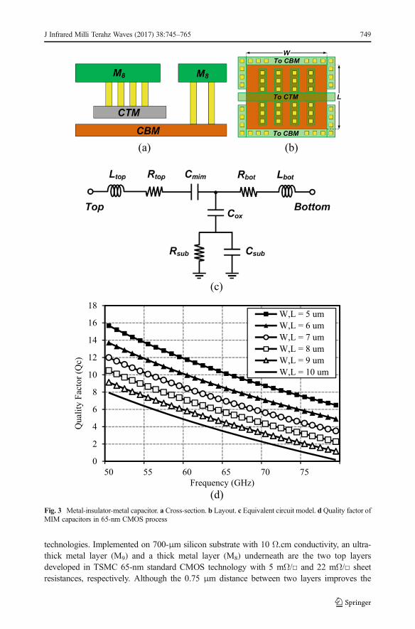
Finally, physically large secondary winding of the stacked and planar series combinersintroduces high output inductance which dramatically reduces the self-resonance frequency(SRF) of transformers because of undesired parasitic capacitance. As a result, the series powercombining structures are not scalable for more than a few amplifiers at millimeter-wavefrequencies as the resonance frequency falls below 60 GHz for complex structures. In addition,a series/parallel tuning capacitor is required to resonate with the inductive output of thetransformer to provide the desirable output matching. The layout, cross-section and theequivalent circuit for metal-insulator-metal (MIM) capacitors designed in 1P9M standard65-nm CMOS technology are shown in Fig. 3. Ultra-thin metal layers (CTM and CBM) withhigh-K dielectric in between are developed in CMOS technology to provide the highestcapacitance per area. Compared to Metal-Oxide-Metal (MOM) and MOS structures, MIMcapacitors are known as the most high-quality linear capacitors in CMOS technology. Thequality factor of these on-chip MIM capacitors are typically low at millimeter-wave frequen-cies [22]. According to the circuit model shown in Fig. 3c, with the increasing frequency, theinductive impedances of the parallel plates (Ltop and Lbot) become comparable to the imped-ance of the series capacitance (Cmim) which results in less total capacitance at higher frequen-cies. In addition, the series resistance of the capacitor plates (Rtop, Rbot) is increased withfrequency because of the skin and proximity effects. The quality factor of several MIMcapacitors ranging with plate sizes of 5 μm× 5 μm to 10 μm× 10 μm is plotted in Fig. 3d.As shown, the quality factor of the MIM capacitors drop from 12 to 5 as the capacitor size isincreased from 55 to 210 fF for the simulated structures. The relatively low-quality factor ofon-chip capacitors has a considerable impact on the power transfer efficiency of millimeter-wave power amplifiers.
3 Proposed Millimeter-Wave Power Combiner
To address the trade-off between the low-quality factor of stacked transformers and lowcoupling factor of planar transformers, we propose a planar multi-conductor power combinerthat can be implemented on the top most layer of the technology while producing the desiredcoupling using multiple primary windings. Figure 1c illustrates the basic idea of the proposedparallel power combining topology. Low loss windings with very high SRF are feasible atmillimeter-wave frequencies with the metal layer available in most standard CMOS
748 J Infrared Milli Terahz Waves (2017) 38:745–765
technologies. Implemented on 700-μm silicon substrate with 10 Ω.cm conductivity, an ultra-thick metal layer (M9) and a thick metal layer (M8) underneath are the two top layersdeveloped in TSMC 65-nm standard CMOS technology with 5 mΩ/□ and 22 mΩ/□ sheetresistances, respectively. Although the 0.75 μm distance between two layers improves the
0
2
4
6
8
10
12
14
16
18
50 55 60 65 70 75
Quali
ty F
acto
r (Q
c)
Frequency (GHz)
W,L = 5 um
W,L = 6 um
W,L = 7 um
W,L = 8 um
W,L = 9 um
W,L = 10 um
(a) (b)
(c)
(d)
Fig. 3 Metal-insulator-metal capacitor. a Cross-section. b Layout. c Equivalent circuit model. d Quality factor ofMIM capacitors in 65-nm CMOS process
J Infrared Milli Terahz Waves (2017) 38:745–765 749

electromagnetic (EM) coupling, the high sheet resistance of M8 increases the power loss. Theproposed topology has the advantage of the higher SRF because of the shorter and higher-Qsecondary traces in comparison with the series power combiners. The challenging aspect ofdesigning the combiner is to choose a topology which can produce the impedance transfor-mation, bias requirements and power combining simultaneously. By implementing bothprimary and secondary winding on the same metal layer, a higher-quality factor is achievableand results in a low loss highly efficient combiner. To achieve a high coupling factor and lowerthe substrate loss, primary windings are implemented on both sides of the secondary winding.
3.1 Power Transfer Efficiency
Three-dimensional electromagnetic (3D EM) simulations are performed to compare thecoupling factor and efficiency of the proposed multi-conductor topology with the stackedand planar transformer-based power combiners. Simulated transmission coefficient (S21) of astacked transformer (Fig. 1a) with the total length of 90 μm, the planar transformer with thesame length (Fig. 1b), and proposed multi-conductor transformer (Fig. 1c) with 90 μm lengthsare illustrated in Fig. 4. Plotted in Fig. 5 for all three structures, effective coupling factorbetween windings is calculated using (1) [23].
K ¼ffiffiffiffiffiffiffiffiffiffiffiffiffiffiffiffiffiffiffiffiffiffiffiffiffiffiffiffiffiffiffiffiffi
Im Z12ð Þ2Im Z11ð Þ:Im Z22ð Þ
sð1Þ
Compared to the other counterparts, the proposed multi-conductor structure shows bettergain performance over a wide bandwidth based on the simulated S21, and the effectivecoupling factor between windings is better than those of the stacked transformer in the desiredfrequency band as shown in Fig. 5. 3D EM simulations have been performed to compare thepower transfer efficiency of the proposed structure and the conventional series power combinerfor different ITRs ranging from 0.1 to 10. Power transfer efficiency of the proposed methodand the conventional series combiner are compared in Fig. 6 based on the maximum availablegain calculations [23]. For ITRs less than unity, the proposed method results in power transferefficiencies higher than 80% for ITRs from 0.4 to 5 which are significantly higher than the
-25
-20
-15
-10
-5
0
10 20 30 40 50 60 70 80 90 100
Tra
nsm
issi
on
co
effi
cien
t ,
S2
1 (
dB
)
Frequency (GHz)
Stacked (Fig.2-a)
Planar (Fig. 2-b)
Multi-Conductor
Fig. 4 Simulated transmissioncoefficient of power combiners
750 J Infrared Milli Terahz Waves (2017) 38:745–765

efficiency obtained by conventional series combiners. For ITRs higher than unity, the proposedstructure still shows higher efficiency for ITRs less than five. As a result, the proposedstructure will be efficient for the case of a four-way combination.
3.2 Elimination of Lossy Tuning Capacitors
Tuning capacitors are required to cancel the output reactance of the power combiners forimpedance matching purpose. These capacitors introduce power loss and create extra paths tothe substrate/ground resulting in reduced overall power transfer efficiency for the powercombiners. A circuit analysis is performed to calculate the impact of the lossy capacitors onthe efficiency of the power combiners in Appendix. Each power combining rail in a powercombiner can be modeled as lossy inductors with mutual inductance between the primary andsecondary traces shown in Fig. 7. Adding a single series tuning capacitor with the load isnecessary to provide the negative reactance to resonate the inductive output of the transformer.Typically, the impact of the tuning capacitor is neglected because of the availability of high-quality capacitors with low equivalent series resistance (ESR) at low GHz frequencies [24].
0.6
0.65
0.7
0.75
0.8
0.85
0.9
10 20 30 40 50 60 70 80
Co
up
lin
g f
acto
r (K
)
Frequency (GHz)
Stacked (Fig2-a)
Planar (Fig. 2-b)
Multi-Conductor
Fig. 5 Simulated coupling factorof on-chip power combiners
50
55
60
65
70
75
80
85
90
95
100
0111.0
Po
wer
Tra
nsf
er E
ffic
ien
cy
Impedance Transformation Ratio
Proposed Combiner
Series Combiner
Fig. 6 Power transfer efficiencyversus ITR for parallel and seriescombiners
J Infrared Milli Terahz Waves (2017) 38:745–765 751

The quality factor of inductors (QL), coupling factor between windings (k), and the qualityfactor of tuning capacitors (QC) are the main parameters which must be considered formillimeter-wave transformer-based impedance matching circuit design. Although the tuningcapacitors can be used to obtain lower turn ration (n) and lower primary inductance for a givenload resistance, but their relatively low-quality factors and high ESR at millimeter-wavefrequencies have a considerable impact on the power transfer efficiency which must be takeninto account at millimeter-wave frequencies. The lossy tuning capacitor is modeled as a seriescapacitor (C) with a finite quality factor of QC. The quality factors of the capacitor and theprimary/secondary inductors are represented by series resistances RC, R1, and R2, respectively.As derived in Appendix, the power transfer efficiency can be represented as a function of thecircuit parameters as
η ¼ kOLð Þ2
kOLð Þ2 þ RLQL
ωL2þ QL
QCþ 1
� � :1
1þ ωL2RLQC
þ ωL2RLQL
: ð2Þ
Equation (2) shows that the power transfer efficiency of any transformer-based powercombiner depends on not only the quality factor of the components but also the size of thesecondary winding, load resistance, and frequency of operation. By eliminating the tuningcapacitors, the power transfer efficiency of the proposed technique will be affected by only thecoupling factor and the quality factors of primary/secondary windings as
η≈1
1k QL
� �2þ 1
k2QLQLD
� �þ 1
; QLD ¼ ωL2RL
ð3Þ
One of the advantages of the proposed power combining topology is the possibility ofeliminating the lossy capacitors. Considering the parasitic capacitance of the transistor stagesand tuning the size of the gap and width of the windings, the proposed power combiner isdesigned to have a very low output reactance. For typical values of coupling factor of 0.7 andquality factor of 15 for windings, the power efficiency of the proposed power combiner can beas high as 85% at 60 GHz.
4 Design of 60-GHz Power Amplifier
A systematic methodology for the design and implementation of the proposed 60-GHz poweramplifiers is developed in this section. The characteristics and technical of the proposed four-
Fig. 7 Half-circuit model of one branch of power combiner
752 J Infrared Milli Terahz Waves (2017) 38:745–765
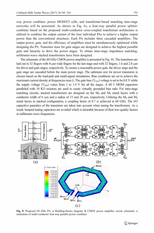
way power combiner, power MOSFET cells, and transformer-based matching inter-stagenetworks will be presented. As shown in Fig. 8a, a four-way parallel power splitter/combiner based on the proposed multi-conductor cross-coupled transformer architecture isutilized to combine the output current of the four individual PAs to achieve a higher outputpower than the conventional structures. Each PA includes three cascaded amplifiers. Theoutput power, gain, and the efficiency of amplifiers must be simultaneously optimized whiledesigning the PA. Transistor sizes for gain stages are designed to achieve the highest possiblegain and linearity to drive the power stages. To obtain inter-stage impedance matching,millimeter-wave stacked transformers have been designed.
The schematic of the 60 GHz CMOS power amplifier is presented in Fig. 8b. The transistors arelaid out in 32 fingers with 4-μmwide fingers for the last stage and with 32 fingers, 1.6 and 2.8 μmfor driver and gain stages, respectively. To ensure a reasonable power gain, the driver stage and thegain stage are cascaded before the main power stage. The optimum size for power transistors ischosen based on the load-pull and small-signal simulations. Bias conditions are set to achieve themaximum current density at frequencies near fT. The gate bias (VGG) voltage is set to be 0.8 Vwhilethe supply voltage (VDD) varies from 1 to 1.8 V for all the stages. A 60 f. MOM capacitorsparalleled with 10 KΩ resistors are used to create virtually grounded bias rails. For inter-stagematching circuits, stacked transformers are designed on the M9 and M8 metal layers with aconductor width of 6 μm and a radius of 15 and 20 μm, respectively. Utilizing the M8 and M9
metal layers in stacked configuration, a coupling factor of 0.7 is achieved at 60 GHz. The I/Ocapacitive parasitics of the transistors are taken into account when tuning the transformers. As aresult, lumped tuning capacitors are avoided which is desirable because of their low-quality factorsat millimeter-wave frequencies.
Po
we
r C
om
bin
er
Po
we
r S
pitter
PA
PA
PA
PA
IN OUT
Gain
Stage
Driver
Stage
Power
Stage
Matc
hin
g
Ne
tw
ork
Matc
hin
g
Ne
tw
ork
VD
D
VDD
VDD
VG1
VG
1
VG1
VG
2V
G2
VG
3V
G3
VD
DV
DD
VD
DV
DD
IN OUT
M1
M1
M1
M1
M2
M2
M2
M2
M3
M3
M3
M3
(a) (b)
(c)Fig. 8 Proposed 60 GHz PA. a Building-blocks diagram. b CMOS power amplifier circuit schematic. crealization of multi-conductor four-way parallel power combiner
J Infrared Milli Terahz Waves (2017) 38:745–765 753

4.1 Multi-conductor Millimeter-Wave Power Combiner
Figure 8c illustrates the physical realization of the proposed power combiner. Two branches ofmulti-conductor planar transformers are connected in parallel to form a four-way combinerwith four primary windings and two parallel secondary windings. The primary and secondarywindings are designed on the ultra-thick metal layer (M9) to achieve the lowest sheet resistanceand consequently highest possible quality factor. By designing the primary windings inadjacent of the secondary winding, frequency response of the proposed structure can becontrolled by the wall-to-wall distance between the windings (S), the width of the primary/secondary windings (W1, W2) and the length of each branch. The primary windings will bederived by individual power amplifiers and RF power will be transferred to the output via theelectromagnetic coupling between the windings. A premier advantage of the proposed struc-ture is to get the maximum available coupling by designing three ultra-thick windings inadjacent. In this case, the primary windings can prevent the extra energy loss on the secondarywindings because of the EM wave penetration in the substrate. Lower wall-to-wall distance oftraces in adjacent results in low parasitic coupling capacitance and increases the SRF. Powercombiner must be able to transform the output impedance of the power transistors to the 50-Ωload while combining the output of four individual stages. The maximum available ITRachieved by the proposed combiner determines the maximum size of the transistors in powerstages. Power transistor with larger channel width and lower output impedance will be feasiblewith the capability of producing a high ITR at 60 GHz. In addition, the SRF of the powercombiner must be far from 60 GHz to prevent the oscillation and instability. To calculate thedesign requirements for different ITRs at 60 GHz, a set of 3D EM simulations is performed.Figure 9 illustrates the achieved ITRs and SRF at 60 GHz for different values of secondary-to-primary width ratio (WR = W2/W1), ITR, and the length of the primary/secondary windings(L). Simulation results show that the higher ITR is achievable by increasing the length of thepower combiner with high WR. By changing the width of the metal traces for a range of 6 to12 μm, the parasitic metal-to-ground capacitance can be controlled to achieve differentinductance for primary/secondary windings. The coupling factor between the secondary/primary windings and the parasitic coupling capacitance can be controlled by changing thespacing distance between the windings (S). The minimum allowable spacing of 2 μm is
0
50
100
150
200
250
300
0
1
2
3
4
5
6
20 70 120 170 220 270
Sel
f re
son
ant
freq
uen
cy (
GH
z)
Imp
edan
ce T
ran
sfo
rmat
ion
Rat
io (
ITR
)
Length (µm)
WR=0.5WR=0.75WR=1.00WR=1.25WR=1.5WR=2.00
Fig. 9 Impedance transformationratio vs. windings length and widthratio
754 J Infrared Milli Terahz Waves (2017) 38:745–765

chosen to achieve highest possible coupling factor while satisfying the process design rulerequirements. The coupling factor also depends on the length of the windings. Windings withlonger traces introduce more mutual inductance and coupling factor. Maximum and minimumpower transfer efficiency of 85 and 70% are achieved based on the achieved transmission lossof −0.55 and −1.5 dB, respectively. To achieve an ITR of 4 to 5, proposed topology with200-μm winding length, width ratio of 1.5 is designed to combine the output power of poweramplifier stages. A power splitter with same architecture is designed at the input to divide theinput power into four amplifier cores. For a very low ITR which is needed at the input, 130-μmlength splitter can split the input power with achieved power efficiency as high as 85%resulting in a higher efficiency compared to using a lossy and non-area efficient Wilkinsonpower divider.
Fig. 10 Fmax of NMOS transistors for different channel widths and current density
0.4
0.6
0.8
1
1.2
1.4
50 55 60 65 70
S-P
aram
eter
s (M
agn
itu
de)
Frequency (GHz)
Meas. S21 Sim. S21
Meas. S11 Sim. S11
Meas. S22 Sim. S22
Fig. 11 S-parameters—simulationand measurements of a powerMOSFET
J Infrared Milli Terahz Waves (2017) 38:745–765 755
4.2 Power Transistor Cells
In addition to lossy passive devices, a major challenge in the design of a fully integrated millimeter-wave PA is the low power gain of the large transistors which are used at such high frequencies. Toprovide a high output power, a transistor with a large channel width is required. Losses due to theparasitic components and the resulting complexity of modeling will increase for these large powertransistors. Hence, the maximum operation frequency (fmax) of power MOSFETs decreases [25].Although the output power is the primary design specification whichmust be satisfied, the gain of aPA must be enough to decrease the linearity constraints of the preceding driver stages. The multi-finger parallel configuration is used to achieve the wider channel width and higher current. Theperformance of this kind of power transistor is determined by three physical parameters, the numberof fingers (Nf), the width of a single finger (Wf), and the number of cells in parallel (M).
Small-signal simulations are performed to choose the optimum size for power transistors.Multi-finger structure with 30 fingers is used to construct transistors with total channel widthsranging from 3 to 150 μm. Transistors are biased at various current bias conditions andmaximum unilateral power gain is used to extract the fmax contours. According to Fig. 10,
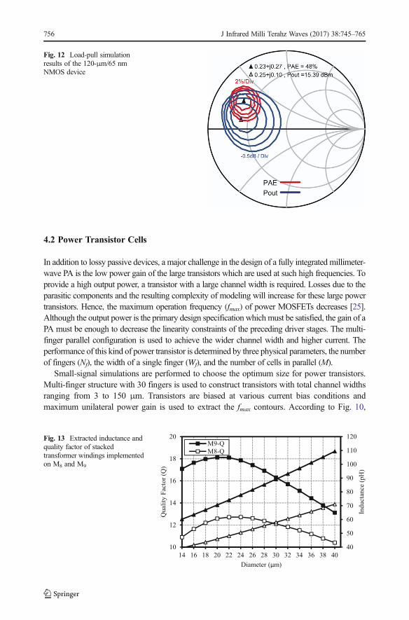
Fig. 12 Load-pull simulationresults of the 120-μm/65 nmNMOS device
40
50
60
70
80
90
100
110
120
10
12
14
16
18
20
14 16 18 20 22 24 26 28 30 32 34 36 38 40
Ind
uct
ance
(p
H)
Qu
alit
y F
acto
r (Q
)
Diameter (μm)
M9-Q
M8-Q
Fig. 13 Extracted inductance andquality factor of stackedtransformer windings implementedon M8 and M9
756 J Infrared Milli Terahz Waves (2017) 38:745–765

using a finger width of 1 to 4 μm with 30 fingers keeps the fmax above 60 GHz. Biased at300 μA/μm, the device can deliver 36 mA current to the load. As most foundry-supplieddesign kits do not offer accurate transistor models at millimeter-wave frequencies, it isnecessary to characterize transistors through fabrication and testing of custom layout powertransistors for the successful design of 60 GHz PAs. Figure 11 demonstrates the large deviationbetween the measured and simulated S-parameters of the fabricated 120-μm power MOSFETat millimeter-wave frequencies. Although an accurate quesi-3D inter-connection electromag-netic (EM) modeling leads to better performance estimation for PAs, the final performance isstill dependent on the power transistors which are not fully characterized for millimeter-wavefrequencies. In addition, the I/O impedances drop when the number of fingers is increasedwhich leads to higher matching network losses because the higher ITR is needed. Load pullsimulations are performed to obtain the optimum impedance required for highest possiblepower/efficiency capabilities. Figure 12 illustrates the load-pull simulation results a powerMOSFET with the total channel width of 120 μm fabricated in 65 nm CMOS technology.Maximum output power of 15.39 dBm is achieved by class A biasing (VGG = 0.9 V and
Fig. 14 Chip micrograph of 60-GHz PA fabricated in 65-nm CMOS
-35
-30
-25
-20
-15
-10
-5
0
5
10
15
20
25
50 53 56 59 62 65 68 71 74 77 80
S P
aram
eter
s (d
B)
Frequency (GHz)
Meas S21 Sim. S21
Meas. S11 Sim. S11
Meas. S22 Sim. S22
Fig. 15 Measured and simulatedS-parameters
J Infrared Milli Terahz Waves (2017) 38:745–765 757

VDD = 1.2 V) with 46% maximum PAE. Normalized optimum load impedance of 0.23 + j0.27is required to obtain such high output power. According to the PAE contours, a high PAE isachievable for a wide range of impedances.
4.3 Transformer-Coupled Inter-stage Matching Network
To ensure a reasonable voltage gain, the driver stage and the gain stage are cascaded before themainpower stage. The second and fist stage transistor sizes are chosen to be 30 and 70% smaller than thepower transistor, respectively, to satisfy the linearity and compression requirements. Stackedtransformers are designed, modeled, and fabricated for 60-GHz inter-stage matching networks.Despite the potential for transformers to be very compact at millimeter-wave frequencies, fortransformer-based millimeter-wave design to be practical, it needs to be demonstrated that theinsertion loss of transformers at these frequencies is better than or comparable to distributedtransmission lines. Furthermore, a predictable and scalable modeling methodology must be devel-oped for a specific technology based on the EM simulations. Basic active and passive devices havebeen implemented, modeled, and verified in CMOS technologies for RF and microwave frequen-cies. However, passive and active models for complex millimeter-wave devices like spiral trans-formers and transmission lines are not available [25, 26]. The substrate loss, thin lossy dielectrics
(a)
(c)
(b)
(d)
0
4
8
12
16
20
0
5
10
15
20
25
-15 -12 -9 -6 -3 0 3
Po
wer
Ad
ded
Eff
icie
ncy
(%
)
Outp
ut
Pow
er
(dB
m)
Input Power (dBm)
Pout
Efficiency
0
5
10
15
20
25
56 58 60 62 64 66
Po
wer
Gai
n (
dB
)
Frequency (GHz)
VDD=1.4 v
VDD=1.0 v
VDD=1.8 v
0
2
4
6
8
10
12
14
16
18
56 58 60 62 64 66
Po
wew
r A
dd
ed E
ffic
ien
cy
(%)
Frequency (GHz)
VDD=1.0 v
VDD=1.4 v
VDD=1.8 v
0
5
10
15
20
25
56 58 60 62 64 66
Outp
ut
Pow
er
(dB
m)
Frequency (GHz)
VDD= 1.0 v
VDD=1.4 v
VDD=1.8 v
Fig. 16 Measured performance of 60 GHz PA. a output power and efficiency. b Power gain variations versussupply voltage. c Saturated output power variations versus supply voltage. d Power-added efficiency variationsversus supply voltage
758 J Infrared Milli Terahz Waves (2017) 38:745–765

Tab
le1
Com
parisonwith
published60
GHzPA
sin
CMOSTechnology
Process
(CMOS)
Frequency(G
Hz)
Stages
VDD
Architecture
P sat(dBm)
P 1dB
(dBm)
Gmax(dB)
PAEmax(%
)P D
C(m
W)
Size
(mm
2 )P s
at/Area
(mW/mm2 )
Ref.
90nm
57–64
31.3
Single-ended/C.S/2X
11.4
6.0
1215.8
44.4
0.40
35[12]
55–71
31.8
Single-ended/C.S/4X
14.5
10.5
2610.2
286
0.64
44[13]
53–68
21.8
Single-ended/Cascode/8x
18.0
11.5
15.5
3.6
1504
0.46
140
[14]
56–62
31.2
Differential/C
.S14.6
1023.2
16.3
135
0.60
48[15]
65nm
58–64
31.0
Single-ended/C.S/2x
17.8
13.8
1112.6
–0.28
215
[16]
58–65
41.8
Differential/C
.S/4x
15.6
13.5
206.6
480
2.25
16[17]
59–67
21.2
Single-ended/C.S
10.6
9.2
13.2
8.9
800.29
158
[27]
47.5
22.8
Class
E,2
-stacked
18.2
–11.2
28.3
–0.24
275
[28]
58–62
31.4
Single-ended/C.S/4x
18.3
16.9
18.8
15.9
424
0.19
356
Thiswork
40nm
57–66
21
Differential/C
.S17
13.8
1730.3
–0.074
675
[29]
28nm
56–67
32.1
Differential/C
.S/2x
16.5
11.7
24.4
12.6
–0.12
371
[18]
28nm
FD-SOI
56–64
31
Single-ended/C.S
18.9
18.2
3517.7
331
0.162
479
[30]
J Infrared Milli Terahz Waves (2017) 38:745–765 759

between layers, distributed effects, and the sheet resistances of metal layers are the technologylimitations that make the models non-applicable for millimeter-wave design.
Stacked octagonal spiral transformers in 65-nm CMOS technology are EM simulated withaverage diameters (D) of 20 to 60 μm using M9 and M8 metal layers. Extracted quality factor andeffective inductances for the transformers are presented in Fig. 13. Simulated at 60GHz, 40–120 pHinductances are achievable by usingM8 andM9metal layers. The insertion loss is determined fromthe S-parameter results by the absolute value of S21. The average extracted insertion loss is 2 dB forvarious sizes of the transformers. The quality factor (Q) and the effective inductance of windings areextracted from Z parameters. The quality factor of the windings is obtained by dividing theimaginary component of the Z11 and Z22 over the real part while the mutual inductance can becalculated by extracting the Z21. The primarywindingwhich is implemented on the ultra thickmetallayer (M9) has the quality factor 60% higher than the secondary winding which is implemented onM8 because of the lower conductor sheet resistance of M9. The average coupling factor of 0.7 ismeasured for one-turn octagonal stacked transformers implemented on M8 and M9.
5 Measurement Results
The proposed 60 GHz PA is fabricated in a 1P9M 65 nm standard CMOS process. The chipmicrograph of the PA is shown in Fig. 14. The PA only occupies a core area of 0.19 mm2 byutilizing the proposed area-efficient power combiner and splitter. Considering all the pads, MOMcapacitors and DC supply rails, the design occupies the total area of 0.42 mm2. The S-parametermeasurements are performed using Agilent N5251A vector network analyzer (VNA) solutionwhich uses an E8361 performance network analyzer (PNA), millimeter-wave test controller andbroadband frequency extenders. The measured S-parameters are compared with the simulationresults as shown in Fig. 15 where a frequency shift of approximately 3 GHz is observed that can beattributed to inaccuracy of the transistor models at millimeter-wave frequencies. Although eachindividual passive component is EM simulated, the EM coupling of these components has not beentaken into account for producing simulation results. Applying 1.4-V supply, a small-signal gain of18.8 and a 3 dB bandwidth of 4 GHz (58 to 62 GHz) are measured. With the stability factor ofgreater than unity, the amplifier is unconditionally stable over the frequency range of operation. The
10
15
20
25
30
56 58 60 62 64 66
OIP
3 (d
Bm)
Frequency (GHz)
VDD =
1.0 VVDD =
1.4 V
Fig. 17 Simulated third-order in-tercept point of the 60-GHz PAover supply voltage variations
760 J Infrared Milli Terahz Waves (2017) 38:745–765

60-GHz power measurements are performed using Rohde-Schwarz NRP-Z power sensors and theRohde & Schwarz ZVA67 VNA. The measured results are shown in Fig. 16a. With 1.4-V supplyvoltage, the saturated output power (Psat) of 18.3 dBm is measured at peak PAE of 15.9%.Compared to the reported 60-GHz PAs in the same and older technologies, the proposed PA issmaller in size for comparable higher output power while improving the linearity based on themeasured 16.9 dBm 1-dB compression point. The measured power gains of the PA for differentlevels of supply voltages are presented in Fig. 16b. The power and efficiency performances are alsomeasured over the IEEE802.15.3c band. As shown in Fig. 16c, d, the PA maintains the 15-dBmoutput power and the average PAE of 10% over the frequency band. Table 1 compares theperformance of the proposed PAwith the state-of-the-art 60 GHz PAs fabricated in 90-, 65-, and28-nmCMOSprocesses. The proposed power amplifier achieves the highest power per area amongthe state-of-the-art of 60-GHz PAs among all 90- and 65-nm implementations while the P1dB andthe Psat are comparable to the reported designs. The linearity of the PA is also characterized by two-tone simulation with a power sweep over 60 GHz band. Two V-band signals with 5-MHz spacingare fed into the input port of the PA and the third-order intercept point (IP3) is extracted fromsimulated third-order inter-modulation distortion plots. Figure 17 shows the simulated output IP3 ofthe proposed 60 GHz PA over supply voltage variations operating inside IEEE 60-GHz band.Although the linearity of the PA is slightly decreased at the edges of the 60-GHz band, it achievesOIP3 of 25.84 dBm at 62 GHz using 1.4-V supply. The average OIP3 of the proposed PA is about9 dB higher than the measured compression point which guarantees a linear operation inside 60-GHz band.
6 Conclusion
A novel multi-conductor power combiner for an integrated 60 GHz CMOS PA has been proposed.The proposed topology provides a compact four-way power combining capability to combine theoutput power of four individual PA cores with higher efficiency compared to the conventionaltransformer-based power combining schemes while occupying smaller die area. The PA coreconsists of cascaded common source stages with inter-stage matching. The peak power gain of18.8 dB and 18.3dBm saturated output power are measured over the 3-dB bandwidth of 4 GHz.The 0.19 mm2 die area consumes 424 mA from a 1.4-V supply and presents 15.9% PAE atsaturation. The proposed power amplifier achieves the highest power density (power/area) com-pared to the reported 60-GHzCMOS power amplifiers in 65 nm or older CMOS technologies up tothe date of this publication.
Appendix
Power Transfer Efficiency Calculations of the Proposed Multi-conductor PowerCombiner
As illustrated in Fig. 7, the equivalent circuit model for one branch of power combiner includesthe primary/secondary winding’s inductances with finite mutual inductance and resistive lossesas R1 and R2, respectively. A tuning capacitor with finite quality factor can be modeled as anideal capacitor in series with the extracted resistance RC. The voltages and currents at the inputand output ports can be determined by Ohm’s law as shown in (4) and (5) to calculate the
J Infrared Milli Terahz Waves (2017) 38:745–765 761

power transfer efficiency of transformer-based power combining networks with considering alllossy elements.
V1 ¼ ZinI1 ¼ Rin þ jXinð ÞI1 ð4Þ
V2 ¼ ZLI2 ¼ RL þ jXLð ÞI2 ð5ÞIt is necessary to evaluate the real part of the input and output impedances to calculate the active
power delivered to the input port or by the output port. In order to find the real part of the inputimpedance (Rin), V1 must be calculated with respect to I1. The current-voltage equation of thenetwork can be written as (6) by applying KVL at the input and output.
V1
V2
� �¼
R1 þ jωL1 − jωM
jωM− RC þ R2ð Þ−j ωL2−
1
ωC
� �
266664
377775
I1I2
� �; M ¼ k:
ffiffiffiffiffiffiffiffiffiffiL1L2
p ð6Þ
where, M is the mutual inductance, k is the coupling factor, and n is the turn ratio between thesecond and first windings. Substituting (5) into (6), relation between I1 and I2 can be found as
I2 ¼ jωM
ZL þ R2 þ RCð Þ þ j ωL2−1
ωC
� � I1 : ð7Þ
Substituting (4) and (7) into the expanded version of (6) gives the (8) which is demon-strating the input voltage with respect to the input current.
V1 ¼ R1 þ jωL1ð Þ I1
− jωMjωMI2
ZL þ R2 þ RCð Þ þ j ωL2−1
ωC
� � ð8Þ
Therefore, the resistance and reactance part of the input impedance can be separated asshown in (9) and (10).
Rin ¼ R1 þ ω2M2 RL þ R2 þ RCð ÞRL þ R2 þ RCð Þ2 þ ωL2− 1
ωC
2 ð9Þ
X in ¼ ωL1−ω2M 2 ωL2−
1
ωC
� �
RL þ R2 þ RCð Þ2 þ ωL2− 1ωC
2 ð10Þ
For power efficiency calculations, it is necessary to demonstrate the input and output powerwith respect to a same current or voltage. Substituting the (9) into the well-known powercalculation expression, (11), gives the input power of the transformer.
762 J Infrared Milli Terahz Waves (2017) 38:745–765

Pin ¼ 1
2Real V1I*1
� �
¼R1
I1 2
2þ 1
2
ωkð Þ2L1L2 RL þ R2 þ RCð Þ I1
2RL þ R2 þ RCð Þ2 þ ωL2− 1
ωC
2ð11Þ
Substituting (7) and (11), the power delivered to the load will then be
Pout ¼RL
I2 2
2
¼ 1
2
RL ωkð Þ2L1L2 I1
2RL þ R2 þ RCð Þ2 þ ωL2− 1
ωC
2 :
ð12Þ
To simplify, at the center frequency, the tuning capacitor (C) and the secondary inductance(L2) must resonate and cancel out each other. The passive power efficiency of the transformer(η) is determined as the power delivered to the load (Pout) over the total power entering thetransformer (Pin), given by
η ¼ RL ωkð Þ2L1L2R2 þ RC þ RLð Þ R1 R2 þ RC þ RLð Þ þ ωkð Þ2L1L2
h i : ð13Þ
The efficiency can be calculated with respect to the quality factor of the circuit components as
η ¼ kOLð Þ2
kOLð Þ2 þ QL
QLDþ QL
QCþ 1
� � :1
1þ QLD
QCþ QLD
QL
: ð14Þ
where the quality factors can be defined as followed.
R1 ¼ ωL1QL1
; R2 ¼ ωL2QL2
; RC ¼ 1
ωCQC; QLD ¼ ωL2
RLð15Þ
Equation (14) proves the huge impact of the lossy capacitor on the power transferefficiency. By eliminating tuning capacitors, the power transfer efficiency of the proposedtechnique will be affected by only the coupling factor and the quality factors of primary/secondary windings as
η≈1
1k QL
� �2þ 1
k2QLQLD
� �þ 1
: ð16Þ
J Infrared Milli Terahz Waves (2017) 38:745–765 763

References
1. T. Mitomo, R. Fujimoto, N. Ono, R. Tachibana, H. Hoshino, Y. Yoshihara, Y. Tsutsumi, and I. Seto, BA 60-GHz CMOS receiver front-end with frequency synthesizer,^ IEEE J. Solid-State Circuits, vol. 43, no. 4, pp.1030–1037, Apr. 2008.
2. D. Dawn, P. Sen, S. Sarkar, B. Perumana, S. Pinel and J. Laskar, "60-GHz Integrated TransmitterDevelopment in 90-nm CMOS," in IEEE Transactions on Microwave Theory and Techniques, vol. 57,no. 10, pp. 2354-2367, Oct. 2009.
3. A. Valdes-Garcia, S. T. Nicolson, J. Lai, A. Natarajan, P. Chen, S. K. Reynolds, J. C. Zhan, D. G. Kam, D.Liu, and B. Floyd, BA fully integrated 16-element phased-array transmitter in SiGe BiCMOS for 60-GHzcommunications,^ IEEE J. Solid-State Circuits, vol. 45, no. 12, pp. 2557–2563, Dec. 2010.
4. O.S.A. Tang, S.M.J Liu, P.C. Chao, W.M. T. Kong, K. Hwang, N. Kirby, and J. Heaton, BDesign andfabrication of a wideband 56- to 63-GHz monolithic power amplifier with very high power-addedefficiency,^ IEEE J. Solid-State Circuits, vol. 35, no. 9, pp. 1298–1306, Sep. 2000.
5. B. A. Floyd, S.K. Reynolds, U.R. Pfeiffer, T. Zwick, T. Beukema, andB.Gaucher, BSiGeBipolar TransceiverCircuits Operating at 60 GHz,^ IEEE J. Solid-State Circuits, vol. 40, no. 1, pp. 156–167, Jan. 2005.
6. U. Pfeiffer et al., "A 60GHz radio chipset fully-integrated in a low-cost packaging technology," 56th
Electronic Components and Technology Conference 2006, San Diego, CA, 2006, pp. 4 pp.7. G. Liu, P. Haldi, T.J. K. Liu, and A. M. Niknejad, BFully integrated CMOS power amplifier with efficiency
enhancement at power back-off,^ IEEE J. Solid-State Circuits, vol. 43, no. 3, pp. 600–609, Mar. 2008.8. Y. Jin, M.A. T. Sanduleanu, and J. R. Long, BA wideband millimeter wave power amplifier with 20 dB
linear power gain and 8 dBm maximum saturated output power,^ IEEE J. Solid-State Circuits, vol. 43, no.7, pp. 1553–1562, Jul. 2008.
9. J. L. Kuo, Z.M. Tsai, K.Y. Lin, and H. Wang, BA 50 to 70 power amplifier using 90 nm CMOS technology,^IEEE Microw. Wireless Compon. Lett., vol. 19, no. 1, pp. 45–47, Jan. 2009.
10. M. Bohsali, A. M. Niknejad, BCurrent combining 60 GHz CMOS power amplifiers,^ in Proc. IEEE RFICSymp., Boston, MA, Jun. 2009, pp. 31-34.
11. Chi Y Law, Anh-Vu Pham, BA High-Gain 60GHz Power Amplifier with 20dBm Output Power in 90nmCMOS,^ in ISSCC, Dig. Of Technical Papers, San Francisco, CA, 2010, pp. 426- 427.
12. J.N. Chang, and Y.S. Lin, B60 GHz CMOS power amplifier with Psat of 11.4 dBm and PAE of 15.8%,^Electronics Lett., vol. 48, no.17, pp. 1038–1039, Aug. 2012.
13. J.F. Yeh, J.H. Tsai, and T.W. Huang, BA 60 GHz power amplifier design using dual radial symmetricarchitecture in 90 nm low power CMOS,^ IEEE Trans. Microw. Theory Tech., vol. 61, no. 3, pp. 1280–1290, Mar. 2013.
14. B. Martineau, V. Knopik, A. Siligaris, F. Gianasello, and D. Belot, BA 53-to-68GHz 18dBm power amplifierwith an 8-way combiner in standard 65nm CMOS,^ in ISSCC, Dig. Of Technical Papers, San Fransisco,CA, 2010, pp. 428- 429.
15. H.Asada,K.Matsushita,K.Bunsen,K.Okada, andA.Matsuzawa,BA60GHzCMOSPowerAmplifierUsingCapacitive Cross-Coupling Neutralization with 16% PAE,^ in EuMC,Manchester, 2011, pp. 1115- 1118.
16. J. Chen, and A. M. Niknejad, BA Compact 1V 18.6dBm 60GHz Power Amplifier in 65nm CMOS,^ inISSCC, Dig. Of Technical Papers, Melbourne, VIC, 2011, pp. 432- 433.
17. Sofiane Aloui, Bernardo Leite, Nejdat Demirel, Robert Plana, Didier Belot, and Eric Kerherve, BHigh-gainand linear 60-GHz power amplifier with a thin digital 65-nm CMOS technology,^ in IEEE Trans. Microw.Theory Tech., vol. 61, no. 6, pp. 2425–2437, June. 2013.
18. S. V. Thyagarajan, A. M. Niknejad and C. D. Hull, "A 60 GHz Drain-Source Neutralized Wideband LinearPower Amplifier in 28 nm CMOS," in IEEE Transactions on Circuits and Systems I: Regular Papers, vol.61, no. 8, pp. 2253-2262, Aug. 2014.
19. M. Farahabadi, K. Moez, BCompact high-power 60 GHz power amplifier in 65 nm CMOS,^ in CustomIntegrated Circuits Conference, San Jose, CA, 2013.
20. D. Chowdhury, P. Reynaert, and A. M. Niknejad, BDesign considerations for 60 GHz transformer-coupledCMOS power amplifiers,^ IEEE J. Solid-State Circuits, vol. 44, no. 10, pp. 2733–2744, Oct. 2009.
21. K. H. An, O. Lee, H. Kim, D. H. Lee, J. Han, K.S. Yang, Y. Kim, J.J. Chang, W. Woo, C.H. Lee, H. Kim,and J. Laskar, BPower combining techniques for fully-integrated CMOS power amplifiers,^ IEEE J. Solid-State Circuits, vol. 43, no. 5, pp. 1064–1075, May. 2008.
22. A. Ghadiri, and K. Moez, BHigh quality factor active capacitors for millimeter wave applications,^ IEEETrans. Microw. Theory Tech., vol. 60, no. 12, pp. 3710–3718, Dec. 2012.
23. H. Gan, BOn-chip transformer modeling, characterization and applications in power and low noiseampllifiers,^ Ph.D. dissertation, Dept. Elect. Eng., Stanford Univ., Stanford, CA, Mar. 2006.
24. I. Aoki, S. D. Kee, D.B. Rutledge, and A. Hajimiri, BFully integrated CMOS power amplifier design using thedistributed active-transformer architecture,^ IEEE J. Solid-State Circuits, vol. 37, no. 3, pp. 371–383,Mar. 2002.
764 J Infrared Milli Terahz Waves (2017) 38:745–765

25. B. Heydari, M. Bohsali, E. Adabi, and A. M. Niknejad, BLow power mm-wave components up to 104 GHzin 90 nm CMOS,^ in Int. Solid-State Circuits Conf. Tech. Dig., San Francisco, CA, Feb. 2007, pp. 200-203.
26. C. Doan, S. Emami, A. Niknejad, and R. Brodersen, BMillimeter-wave CMOS design,^ IEEE J. Solid-StateCircuits, vol. 40, no. 1, pp. 144–155, Jan. 2005.
27. S. Aloui, Eric Kerherve, R. Plana, and D. Belot, BA 59GHz to 67GHz 65nm CMOS High Efficiency PowerAmplifier,^ in New Circuit and Systems, Bordeaux, France, 2011, pp. 225- 228.
28. A. Chakrabarti and H. Krishnaswamy, "High-Power High-Efficiency Class-E-Like Stacked mmWave PAsin SOI and Bulk CMOS: Theory and Implementation," in IEEE Transactions on Microwave Theory andTechniques, vol. 62, no. 8, pp. 1686-1704, Aug. 2014.
29. D. Zhao and P. Reynaert, "A 60-GHz Dual-Mode Class AB Power Amplifier in 40-nm CMOS," in IEEEJournal of Solid-State Circuits, vol. 48, no. 10, pp. 2323-2337, Oct. 2013.
30. A. Larie, E. Kerhervé, B. Martineau, L. Vogt and D. Belot, "2.10 A 60GHz 28nm UTBB FD-SOI CMOSreconfigurable power amplifier with 21% PAE, 18.2dBm P1dB and 74mW PDC," 2015 I.E. InternationalSolid-State Circuits Conference - (ISSCC) Digest of Technical Papers, San Francisco, CA, 2015, pp. 1-3.
J Infrared Milli Terahz Waves (2017) 38:745–765 765


![School of Biomedical Engineering, Science & Health Systems V 1.0 SD [020327] Kambiz Pourrezaei, Ph.D. Drexel University.](https://static.fdocuments.net/doc/165x107/551672e6550346a2698b5891/wwwbiomeddrexeleduresearchportfolio-school-of-biomedical-engineering-science-health-systems-v-10-sd-020327-kambiz-pourrezaei-phd-drexel-university.jpg)