
Applying Microwave Technology in Short Range Radio
83
Transcript of Applying Microwave Technology in Short Range Radio

THESIS FOR THE DEGREE OF DOCTOR OF PHILOSOPHY
Applying Microwave Technology in
Short Range Radio Communication and
Sensing SystemsTheory and Design
by
Emil Nilsson
Microtechnology and Nanoscience (MC2) School of Information Science, ComputerChalmers University of Technology and Electrical Engineering (IDE)
SE-412 96 Göteborg, Sweden Halmstad UniversityBox 823
SE-301 18 Halmstad, Sweden
Göteborg, Sweden 2013

Applying Microwave Technology in Short Range Radio Communication andSensing Systems - Theory and Design
c© Emil Nilsson, 2013
ISBN 978-91-7385-914-1
Doktorsavhandlingar vid Chalmers tekniska högskolaNy serie nr 3595ISSN 0346-718X
Technical Report MC2-264ISSN 1652-0769
Microwave Electronics LaboratoryDepartment of Microtechnology and Nanoscience - MC2Chalmers University of TechnologySE-412 96 Göteborg, SwedenPhone: +46 (0)31 772 1000
School of Information Science, Computer and Electrical Engineering (IDE)Halmstad UniversityBox 823, SE-301 18 Halmstad, SwedenPhone: +46 (0)35 16 7100
Cover illustration: Short range communication and sensing, by Elias Nilsson.
Printed by Chalmers Reproservice Göteborg, Sweden 2013
Abstract
Microwave technology continues to reach new areas and applications. Microwavebased sensors create the possibility to sense objects in remote and hostile envi-ronments, while miniaturization makes the merge of radios, sensors, and com-puting into new small devices possible. Bridging the communication of the last10 meters from numerous physical devices to a global network must be donewireless. Short range radio communication technology represents the most re-alistic untethered technology at hand.
Advanced digital control and processing electronics enable realization of so-phisticated functionality and sophisticated communication protocols, also in lowcost small size radio nodes. The high level of integration today common for dig-ital electronics is increasingly utilized in analog electronics.
The need for small low power transceivers in many new applications is mo-tivated by limited physical space and maintenance cost. The energy source forthe device (usually a battery) sets the life time, the cost, and in some casesthe physical dimensions of the nal product. Low power electronics enable theuse of more agile energy sources and longer lifetime with smaller batteries andenergy harvesting techniques.
In this thesis a low power transceiver hardware and MAC protocol are pro-posed and investigated. A theory estimating noise in an envelope detector sub-ject to a blocking signal is developed and used as a knowledge base for imple-mentation of a Wake-up radio. The small Wake-up radio consumes 2.3µW and isdesigned in 130 nm CMOS using no other external components than the carriersubstrate its mounted on. A survey of recently published low-power receiversis compared with estimation of lowest power consumption with optimized re-ceiver topologies. Finally, the design of a low output-power radar interferometricsensor for industrial applications is presented together with measurements andsimulations.
i

ii

Acknowledgment
There are many people I wish to thank, who have supported me in my work.First I would like to mention Bertil Svensson, Urban Bilstrup, and Pelle Wibergat Halmstad University for always being a great support, and of course all thepeople at MPE-lab. Thanks also go to my supervisor Peter Linnér, and to LarsSvensson at Chalmers for helpful technical discussions. Special thanks go tothe people at ISY in Linköping who helped me with the CMOS implementa-tions, Jonas Fritzin, Jacob Wikner, Atila Alvandpour, and many more. Thesingle most important person for the nalization of this work has been ChristerSvensson, thanks for all your ideas and help over time. Some special thanks andthoughts go to Johan Malm, who unfortunately has some rough times ahead.Johan has always been helpful, and open for a good technical debate. I wishyou and your family the best. Finally I thank my family and friends for justbeing around and always up to new adventures.
iii

iv
List of publications
I. Emil Nilsson, Björn Nilsson, Lars Bengtsson, Bertil Svensson, Per-Arne Wiberg, and Urban Bilstrup, A Low Power-Long Range ActiveRFID-system Consisting of Active RFID Backscatter Transponders, IEEEInternational Conference on RFID-Technology and Applications 2010, June2010.
II. Emil Nilsson, Peter Linnér, Arne Sikö, Urban Bilstrup, and Per-Arne Wiberg, A New CMOS Radio for Low Power RFID Applications,IEEE International Conference on RFID-Technology and Applications 2010,June 2010.
III. Emil Nilsson and Christer Svensson, Envelope Detector Sensitivity andBlocking Characteristics, 20th European Conference on Circuit Theoryand Design, ECCTD 2011, Linköping, Sweden, August 28-31, 2011.
IV. Emil Nilsson and Christer Svensson, Ultra Low Power Wake-up Radio us-ing Envelope Detector and Transmission Line Voltage Transformer, IEEEJournal on Emerging and Selected Topics in Circuits and Systems, March2013.
V. Emil Nilsson and Christer Svensson, Power Consumption of IntegratedLow-Power Receivers, submitted for publication.
v

vi

List of publications from
Licentiate thesis
VI. Emil Nilsson and Donald Malmberg, Using microwave technology to cre-ate a topographical image of the burden surface in a blast furnace, Pro-ceedings of 5th Ironmaking Conference, Buenos Aires, November 2005.
VII. Emil Nilsson and Lars Baath, Radar Interferometric Measurements witha Planar Patch Antenna Array, IEEE Sensors Journal, pp. 1025-1031,July 2007.
VIII. Emil Nilsson and Donald Malmberg, Using microwave interferometry toimprove the blast furnace operation, Scanmet III 3rd International Con-ference on Process Development in Iron and Steelmaking, Luleå, Sweden,8-11 June 2008.
vii

viii

Other publications
IX. Emil Nilsson and Martin Löfgren, A GaAs MMIC Star Mixer for Ku-bandSpace Applications, Swedish National Symposium GHz 2000, March 2000.
X. Donald Malmberg, Pär Hahlin, and Emil Nilsson, Microwave Technologyin Steel and Metal Industry, an Overview, ISIJ International, Vol. 47,No. 4, pp. 533-538, 2007.
XI. Emil Nilsson, Björn Nilsson, and Eric Järpe, A Pharmaceutical Anti-counterfeiting Method Using Time Controlled Numeric Tokens, IEEE In-ternational Conference on RFID-Technology and Applications 2011, Septem-ber 2011.
XII. Emil Nilsson, Björn Nilsson, Urban Bilstrup, and Per-Arne Wiberg, UltraLow Power Radio for Pervasive Computing, Embedded conference Scan-dinavia 2011, October 2011.
XIII. Johansson Anders, Kubicka Jiri, Nilsson Emil, Wiebols Eric, Nilsson An-ders, and Lindvall Martin, An apparatus for detecting, measuring and se-lecting physiological signals and a method thereof, Patent PCT 2002096287,December 2002.
XIV. Emil Nilsson and Lars Baath, Multi-dimensional imaging method andapparatus, Patent US20070109177, May 2007.
XV. Urban Bilstrup, Emil Nilsson, and Per-Arne Wiberg, A device for wirelessoperation and method for operating the device, Patent PCT 2008026988,March 2008.
XVI. Urban Bilstrup, Emil Nilsson, and Per-Arne Wiberg, Method and devicefor adjusting sensitivity, Patent PCT 2009108106, September 2009.
ix

x
Preface
This thesis consist of two parts, one part about short range radio communica-tion, and one part containing research on a interferometric sensor. Initially Istarted my research looking into sensors based on interaction between matterand electromagnetic waves using interferometric receiver and antenna array se-tups. I was mainly focusing on how to form a sensing beam, and how the signalshould be processed to extract the intended information. The actual hardwarewas of limited interest, but had to deliver a decent signal. Important to considerwas the noise contribution, and even more the phase stability; an interferometricsystem depend largely on information carried by the phase of the signal. Thesensor system was intended for an interferometric topographical imaging systemin a blast furnace and is covered by patent [1].
The reasons for not completing my PhD at this time were of both privateand external origin; RWI, the company founded by my supervisor Lars Bååth,and where I pursued my research, moved its business to Lund. I could notaccompany at this time since I was enjoying parental leave with two sweettoddlers.
During the work with the hardware platform enabling the interferometricmeasurements I developed an interest in the possibilities with integration of elec-tronics, and especially analog high frequency electronics. Increased integration,as a mean for improved signal integrity and smaller form factor, highlighted theissue of power aware design of the sensor. By assigning a dedicated transceiverfor each individual array antenna element a faster and more reliable imagingwould be possible, but it would also increase the power density.
When scouting for new projects to continue my research I was asked to lookinto the design of low power radio electronics for RFID applications. This areacombines analog electronics and high integration in a very challenging way. Thereason for the emerging interest in this area was the ongoing development to-wards ecient short range radio communication solutions. Today this is partof a developing eld, popularly termed Internet of Things (IoT), which actu-ally includes areas such as RFID, Wireless Sensor Networks (WSN), IntelligentTransport Systems (ITS), and much more.
The development of RFID systems consider both hardware and mediumaccess (MAC) protocols. In communication systems a better performance canbe reached by co-design, or cross-layer design, of hardware and communicationprotocols. Our proposed system tried to make use of a very simplistic receiver,and a tailor made MAC protocol. Usually RFID nodes have a very limitedpower budget, and the reader has to do the major part of energy demandingprocessing. The number of applications possible to reach with the technologydepend heavily on how much energy each node require and how much energy it
xi

can store.Common for many IoT applications, including RFID, is the need for an
always aware radio receiver, a Wake-up Radio (WuR). The energy storage lifetime sets the system life time, maintenance cost, unit cost, and in some casesthe size, of the nal product. Development of low power electronics enables theuse of smaller batteries, longer lifetime, or energy harvesting techniques to beused.
Thus, the work continued with focus on the Wake-up functionality. Howto integrate and minimize the footprint of the receiver, and how to analyzeand predict detector sensitivity in a modern radio environment with stronginterference.
xii

Contents
1 Introduction 1
1.1 Motivation . . . . . . . . . . . . . . . . . . . . . . . . . . . . . . 11.2 Aim of this study . . . . . . . . . . . . . . . . . . . . . . . . . . . 11.3 Thesis contributions . . . . . . . . . . . . . . . . . . . . . . . . . 21.4 Summary of appended papers . . . . . . . . . . . . . . . . . . . . 2
2 Low power short range radio communication 7
2.1 Background . . . . . . . . . . . . . . . . . . . . . . . . . . . . . . 92.1.1 Receivers for low power applications . . . . . . . . . . . . 92.1.2 Related work . . . . . . . . . . . . . . . . . . . . . . . . . 10
2.2 A low power RFID-system with a specically designed MAC pro-tocol . . . . . . . . . . . . . . . . . . . . . . . . . . . . . . . . . . 132.2.1 Principle of operation . . . . . . . . . . . . . . . . . . . . 142.2.2 Results and discussion . . . . . . . . . . . . . . . . . . . . 15
2.3 A low power oscillator-free CMOS TRF receiver . . . . . . . . . 172.3.1 Description of the receiver architecture . . . . . . . . . . . 172.3.2 Results and discussion . . . . . . . . . . . . . . . . . . . . 21
2.4 Analysis of lower bound for WuR energy consumption . . . . . . 242.4.1 Description of parameter set and analysis . . . . . . . . . 242.4.2 Results and discussion . . . . . . . . . . . . . . . . . . . . 32
3 A microwave based imaging sensor 33
3.1 Background . . . . . . . . . . . . . . . . . . . . . . . . . . . . . . 333.1.1 Contact free measurements with radar . . . . . . . . . . . 333.1.2 Interferometry . . . . . . . . . . . . . . . . . . . . . . . . 34
3.2 Description of experimental radar interferometer . . . . . . . . . 393.2.1 Signal system . . . . . . . . . . . . . . . . . . . . . . . . . 413.2.2 Interferometer array design . . . . . . . . . . . . . . . . . 44
3.3 Results and discussion . . . . . . . . . . . . . . . . . . . . . . . . 48
4 Conclusion and outlook 55
4.1 Conclusion . . . . . . . . . . . . . . . . . . . . . . . . . . . . . . 554.2 Outlook . . . . . . . . . . . . . . . . . . . . . . . . . . . . . . . . 56
xiii

xiv

Acronyms and terms
ADC Analog to Digital Converter.A-RFID Active-RFID.ASIC Application Specic Integrated Circuit.ASK Amplitude Shift Keying.BAW Bulk Acoustic Wave.BER Bit Error Rate.BIST Built In Self Test.CLEAN Numerical deconvolving process.CMOS Complementary Metal Oxide Semiconductor.CW Continuous Wave.EM Electromagnetic.EPC Electronic Product Code.ESD ElectroStatic Discharge.FMCW Frequency Modulated Continuous Wave.FPGA Field Programmable Gate Array.FR4 Glass-reinforced epoxy laminate sheets.FSK Frequency Shift Keying.ID IDentity.IF Intermediate Frequency.IoT Internet of Things.IP Intellectual property.IR Infra Red.ISM Industrial, Scientic and Medical (radio bands).ITS Intelligent Transport System.LNA Low Noise Amplier.LO Local Oscillator.MAC Medium Access Control.MEFOS Swedish metallurgical research institute.MEM Maximum Entropy Method.MEMS MicroElectroMechanical systems.MIM Metal Insulator Metal.MOS Metal Oxide Semiconductor.MOST MOS Transistor.OOK On-O Keying.PCB Printed Circuit Board.PLL Phase Locked Loop.PSF Point Spread Function.PSK Phase Shift Keying.
xv

Acronyms cont.
QAM Quadrature Amplitude Modulation.RCS Radar Cross Section.RF Radio Frequency.RFID Radio Frequency IDenticaion.SAR Synthetic Aperture Radar.SDR Software Dened Radio.SNR Signal to Noise Ratio.TRF Tuned RF.UWB Ultra Wide Band.VCO Voltage Controlled Oscillator.WLAN Wireless LAN.WSN Wireless Sensor Network.WuR Wake-up Radio.
xvi

Chapter 1
Introduction
1.1 Motivation
Sensors embedded in networking and computing devices are predicted to gener-ate a major part of the information carried over the internet in the near future.Already sometime between 2008 and 2009 there were more devices than peopleconnected [2]. Miniaturization of computers, transceivers, and sensors continuesand new services will be available. The evolution of an ubiquitous internet andglobal covering cellular network has called for new ways of looking at communi-cation. Ad-hoc communications connect physical devices and sensors all aroundus with computing resources and networks around the world. However, a per-sisting hurdle for this vision of the Internet of Things (IoT) is the remaining 10meters before reaching out to each device and object being sensed.
Short range low power microwave systems represent the only realistic tech-nology to overcome this short but challenging distance, and thus such systemshave to be utilized within new areas and applications; for communications pur-poses or as a part of sensor technologies.
1.2 Aim of this study
The aim of this study has been to address some important questions raised onthe implementation of microwave electronics in short range radio communicationand sensing.
How can we expand the utilization of microwave technology in communica-tion and sensing? What limitations are imposed on technology from:
• environment
• market (cost)
• required coexistence with other systems
Are new ways in thinking of radio needed to reach otherwise inconceivable ap-plications?
The research approach has been to develop new system solutions with realand commercial applications in mind. To understand and specify target per-formance, and interpret requirements into design parameters. To nd limiting
1

CHAPTER 1. INTRODUCTION
factors for reaching successful implementation. To nd, investigate, and im-prove some of the most important components of the system. Finally the ideashave been tested by simulation and implementation of real electronic systems.
1.3 Thesis contributions
• A proposed low-power transceiver architecture combined with a novelmedium access protocol design.
• Implementation of low-frequency prototype of a low-power transceiver.
• Analytical expressions for impact of noise and blocker on the envelopedetector.
• Monolithic implementation of ultra low-power high-frequency receiver.
• Measurement on integrated low-power envelope detector with blockingsignal.
• System analysis of low power Wake-up Radios (WuR).
• Investigations on how 3D-imaging could improve a blast furnace operation.
• Development of 3D-imaging microwave interferometry system for indus-trial application.
• Measurements with 3D-imaging microwave interferometer.
1.4 Summary of appended papers
Paper I
A Low Power-Long Range Active RFID-system Consisting
of Active RFID Backscatter Transponders
Summary
In this paper we present a novel active radio-frequency identication system con-sisting of transponders with low complexity, low power consumption, and longsystem-reading range. The transponder's low complexity and small circuit inte-gration area indicate that the production cost is comparable to the one of a pas-sive tag. The hardware keystone is the transponder's radio wake-up transceiver,which is a single oscillator with very low power consumption. The communica-tion protocol, based on frequency signalling binary tree (see Sect. 2.2.1), con-tributes to the low complexity of the tag architecture. More than 1500 tags canbe read per second. The average transponder ID read-out delay is 319 ms whenthere are 1000 transponders within reach of the interrogator. The calculatedexpected life time for a transponder is estimated to be almost three years.
2

1.4. SUMMARY OF APPENDED PAPERS
Paper II
A New CMOS Radio for Low Power RFID Applications
Summary
A novel radio receiver circuit, functioning as a tuned active and detecting an-tenna, is described. The receiver is suggested to be part of a new radio systemwith the potential of competing with the range capability of active RFID-tagsand, through its low power and long lifetime, with passive RFID-tags. Thecircuit is outlined and the functionality is veried by simulations and measure-ments. A 24 MHz discrete prototype showed better than -70 dBm sensitivityand 5 kHz bandwidth, with a power consumption of 102 µW. Simulations of amonolithic implementation were performed at 2.5 GHz. The detector is mod-elled by using 180 nm CMOS transistors. In simulations the power consumptionfor the detector is below 125 µW at a sensitivity of -83 dBm and a bandwidthof 9 MHz. Our conclusion is that this novel simple circuit architecture is wellsuited for monolithic implementation of a low power transceiver.
Paper III
Envelope Detector Sensitivity and Blocking Characteris-
tics
Summary
This paper presents analytical expressions for the sensitivity of a low powerenvelope detector driven by a weak RF signal in the presence of a blocking signal.The envelope detector has been proposed for low power WuR's in applicationssuch as RFID and wireless sensor systems. The theoretical results are veriedwith simulations of a modern short channel MOS transistor in a commonly usedcircuit topology. A discussion around a tutorial example of a radio frontend,consisting of an LNA and a detector, is presented. It is shown that the sensitivityof a low power envelope detector can reach -62 dBm with a low power LNA andin presence of a CW blocker.
Paper IV
Ultra Low Power Wake-Up Radio using Envelope Detector
and Transmission Line Voltage Transformer
Summary
An ultra-low power wake-up radio receiver using no oscillators is described. Theradio utilizes an envelope detector followed by a baseband amplier and is fab-ricated in a 130nm CMOS process. The receiver is preceded by a passive RFvoltage transformer, also providing 50 Ω antenna matching, fabricated as trans-mission lines on the FR4 chip carrier. A sensitivity of -47 dBm with 200 kbpsOOK modulation is measured at a current consumption of 2.3 µA from a 1 Vsupply. No trimming is used. The receiver accepts a -13 dBm CW blockingsignal, or modulated blockers 6 dB below the sensitivity limit, with no loss ofsensitivity.
3

CHAPTER 1. INTRODUCTION
Paper V
Power Consumption of Integrated Low-Power Receivers
Summary
With the advent of Internet of Things (IoT) it has become obvious that RFdesigners have to be aware of power constraints, e.g. in the design of simplisticultra-low power receivers acting as Wake-up radios (WuR). The objective of thiswork, one of the rst systematic studies of power bounds for RF-systems, is toprovide an overview and intuitive feel for how power consumption and sensitivityrelate for WuRs. This was done by setting up circuit schematics for dierentradio receiver architectures to nd analytical expressions for their output signal-to-noise ratio including power consumption, bandwidth, sensitivity, and carrierfrequency. The result of the analytical expressions and optimizations of thecircuits are energy per bit versus sensitivity, which are then compared withrecent published low power receivers. The parameter set used in the analysis ismeant to reect typical values for integrated CMOS fabrication processes, andtypical small sized RF lumped components.
Paper VI
Using microwave technology to create a topographical im-
age of the burden surface in a blast furnace
Summary
In this paper a novel approach to use radar interferometry technology to createa 3D topographical image of the burden surface is described. By this approachthe drawbacks of the presently used technologies used for burden surface deter-mination are expected to be eliminated. MEFOS has tested an antenna unitthat has the potential of measuring the full burden surface continuously duringoperation in the blast furnace and presents the result as a topographical im-age of the burden surface or a 3D image. Trials have so far been performed inlaboratory as well as in a full scale charging model with promising result.
Paper VII
Radar interferometric measurements with a planar patch
antenna array
Summary
A planar patch antenna array has been made for radar interferometry. Theantenna array consists of 32 rectangular patches on a ceramic loaded teon sub-strate. The patches are individually coupled to the microwave electronics intwo orthogonal circular polarizations. The radar interferometer is intended fortopographic imaging in industrial environment, in this case a blast furnace pro-ducing hot metal for the steel and metal industry. Ordinary imaging techniqueswith IR or visible radiation are not possible to use due to high temperatures anddue to scattering from dust and particles. A model of a blast furnace burdenmaterial surface (see Fig.3.9) was measured and detected.
4

1.4. SUMMARY OF APPENDED PAPERS
Paper VIII
Using microwave interferometry to improve the blast fur-
nace operation
Summary
There are many known technologies that can be used to monitor surfaces, butmost of them requires a transparent environment to be functional. In the blastfurnace where the environment is full of dust and fume at high temperaturesthose technologies are not applicable. With a functional technology in such anenvironment the burden surface could be analyzed and monitored, which in itsextension would lead to a way to control the charging operation in the blastfurnace and thus a better use of raw material and also a better gas utilization.In this paper we will discuss the use of microwave technology as one technologywith the potential to create a topographical image of the burden surface in theblast furnace during operation.
5

CHAPTER 1. INTRODUCTION
6

Chapter 2
Low power short range radio
communication
Power has for a long time been the dominant design constraint for digital elec-tronics. Among the motives we nd the need to reduce cost for cooling andpower, and the need for prolonged time between charges of mobile devices. Inanalog electronic design, and especially RF electronic design, the drive to reducepower has not been the same. Traditional RF electronic design has been moreabout getting better performance from given devices. However, along with thedevelopment of personal mobile communication also RF designers have becomeincreasingly aware of the power issue. RF electronics have gradually becomemore integrated on ASIC devices together with the digital electronics, and thusare being subject to the same fabrication processes (mainly CMOS) and to thesame scaling rules.
With the ongoing realization of the vision of Internet of Things (IoT), it hasbecome even more obvious that RF designers have to be aware of the powerconstraint [3]. Sensors within the IoT have to survive on a single battery duringtheir projected lifetime, or live on any available and harvested energy in itssurroundings [4]. It would be virtually impossible to change batteries on eachdevice in the considered swarm of connected items. For the most slimmeddown sensors, communication has to be provided solitary by WuRs or similarsimplistic radios. The communication distance is often short and require lowpower solutions, often referred to as short range devices.
There is no clear denition of what short range radio communication is, buta common view seems to be radio communication over a shorter range than 10meters. New functionalities and applications may be reached if we can overcomethese last 10 meters without wires, using low power wireless devices. From theETSI homepage [www.etsi.org] we nd the following description of what "ShortRange Device" might include:
Short Range Devices (SRD) are radio devices that oer a low riskof interference with other radio services, usually because their trans-mitted power, and hence their range, is low. The denition 'ShortRange Device' may be applied to many dierent types of wirelessequipment, including various forms of:
7

CHAPTER 2. LOW POWER SHORT RANGE RADIO COMMUNICATION
• Access control (including door and gate openers)
• Alarms and movement detectors
• Closed-circuit television (CCTV)
• Cordless audio devices, including wireless microphones
• Industrial control
• Local Area Networks
• Medical implants
• UWB Sensors and Radars (such as ground probing radar)
• Remote control
• Radio frequency identication (RFID)
• Road Transport Telematics
• Telemetry
Short range devices often benet from a relaxed regulatory regimecompared with other radio communications equipment. As generalprinciple, a user is licence free to operate such equipment, somespecic cases may require an individual licence.
The importance of the power issue for short range radio communication isunderlined by the following citations.
In the annual report 2012 of Berkeley Wireless Research Center it is writ-ten:
"Wireless systems are evolving to a three tiered environment with aubiquitous, embedded and transparent sensory swarm at the outerlayer. Ultra-low-power realizations of integrated wireless sensor nodesare an essential condition for the swarm concept to become trulysuccessful."
According to a an article in EETIMES, Nordic Semiconductor's CEO,Svenn-Tore Larsen, said:
Once designers have an inexpensive way to add an interoperablewireless link to anything that's battery powered, even devices withthe smallest batteries, the application potential is vast. Designerswill come up with thousands of ways to use that link.
Research should aim at lowering the threshold for adding the wireless link.This can be accomplished by reducing the footprint, merging to commerciallyfeasible technology bases, and not least, by reducing the power consumption.Parameters like linearity and sensitivity has often been prioritized over powerconsumption in wireless system work. More energy ecient hardware has re-duced the energy demand, but system design has not been focusing on reachingleast possible overall power consumption. This has changed and today powerconsumption is in focus from components through all system levels in radioengineering.
8

2.1. BACKGROUND
fBB
Antenna
fRF
+ Demod
Figure 2.1: Regenerative receiver. The positive feedback loop improves the gainof the pre-amplier. The feedback is kept below the level feeding a self oscillation.
fBB
Antenna
fRF
fLO>2fIF
+ Demod
Figure 2.2: Superregenerative receiver with a quench (sampling) oscillator. Thepositive feedback is periodically adjusted by the quench oscillator from a low levelup to a level sustaining self-oscillation in the loop.
2.1 Background
2.1.1 Receivers for low power applications
The set of available low power receiver architectures is rather limited. Lowpower radio solutions often use simple modulation schemes like ASK or FSK,with some exceptions such as the injection locked PSK receiver described in [5].
During the highly innovative radio era of the early 1900's, topologies such asthe regenerative receiver, Fig. 2.1, and the super-regenerative receiver, Fig. 2.2,were invented. The regenerative and super-regenerative receivers use feedbackto get the most out of poor ampliers and devices. The positive loop gain ofthe regenerative receiver is kept below the level allowing self oscillation to buildup ("the same signal is amplied many times"). This way gain is increasedand selectivity is improved at the same time. While for the super-regenerativereceiver the loop gain is repeatedly adjusted to allow self-oscillation to buildup [6]. The loop gain is here controlled by the quench oscillator. The receivedsignal is sampled at the quench frequency, and the oscillation builds up fasterfor stronger signal levels. Actually the regenerative receiver may also be used ina self-oscillation mode, for reception of CW signals (morse code). The feedbackloop works both as an amplier and as a heterodyne oscillator in this mode(oscillation frequency is set slightly oset to the CW frequency).
The promising properties of the regeneration phenomenon makes the regen-erative and super-regenerative receivers candidates for low power radio. How-ever, problems with stability and control seem to have prevented them frommaking true success.
The Tuned RF receiver (TRF) (also this is a revoked design from earlyradio), see Fig. 2.3, is basically a crystal radio and uses no oscillators. The
9

CHAPTER 2. LOW POWER SHORT RANGE RADIO COMMUNICATION
fBB
Antenna
fRF
Demod
Figure 2.3: Tuned RF receiver, TRF.
TRF consists of an RF-lter and a pre-amplier together with an envelopedetector. A transformer may give passive voltage gain and provides some RF-ltering before the detector. This passive gain is no real power gain but onlytrades current for voltage by increasing the impedance level. If we want touse a common CMOS process for implementation, the energy detector can bedesigned with MOS transistors as the rectifying components. The envelopedetector eciency strongly depends on the RF carrier amplitude VRF . Theoutput baseband voltage is VO = kV 2
RF , where k is a coecient depending ontechnology and eciency. Better sensitivity is reached by reducing bandwidthof the baseband lter, and thereby reducing channel capacity. The selectivity issolely depending on the RF-lter, and is rather poor.
It is worth noting that alos the superheterodyne is a candidate for low powerradio, although hampered by having an always running local oscillator (LO)draining energy. The superheterodyne will be further treated in the thesis insection 2.1.2 and section 2.4.1.
2.1.2 Related work
The Berkeley PicoRadio project [7] has worked on ad-hoc sensor nodes andtheir system level requirements. They have identied the radio communicationdata link as one of the most challenging parts of these systems. According toBerkeley each node has to: use very small amounts of power to enable the useof energy scavenging (<100µW), have a low cost implementation (<1$US), andhave a small form factor (<cm−3). That is for a complete sensor node, if itshould be used ubiquitously. The small form factor imposes severe limitationson the antenna eciency, and research work on solutions better exploiting theavailable volume of each node [8]. Further, wireless sensor nodes are required tofunction in a multitude of environments, embedded in or in close proximity to alarge variation of materials such as metal, human tissue, air, etc. This requiresdierent types of antennas and/or adaptive matching as in [9] and [10].
A survey of recent published low power receivers is found in, Fig. 2.4, wherethe consumed energy to receive a single bit is plotted as a function of the receiversensitivity. The sensitivity is dened as the RF power needed to reach a raw biterror rate of BER=10−3, before redundant coding and error corrections. Thepublished receivers are used in applications ranging from general use in WSNto more spectacular use such as the heavy duty cycled receiver for e.g. insectight control in [11]. Passive RFID nodes have inherently low sensitivity, sincethey are supplied by the incoming RF-energy being scavenged [12][13]. Thepassive transceivers using load-modulation have the drawback that they needto be optimized both for sensitivity to and rectication of the incoming radioenergy. In [14] a passive "frequency conversion" data transmission method is
10

2.1. BACKGROUND
-120 -110 -100 -90 -80 -70 -60 -50 -40 -30 -2010
-4
10-3
10-2
10-1
100
101
102
103
Cheng2012Cheng2012
Hambeck2011
Roberts2012
Vouilloz2001
Joehl2001
Wong2008
Otis2005
Bohorquez2009
Bohorquez2009
Gerosa2009
Solda2011
Ayers2010
Daly2010
Ayers2010
Pletcher2009
Solda2011
Kolinko2007
Crepaldi2010Daly2007
Nilsson2012
Daly2007
Kwon2012
Curty2005
Roover2010
Daly2010Huang2010
Huang2010
Chen2007
Kim2012
Sensitivity [dBm]
DC
ene
rgy
per
bit [
nJ]
Survey of published low-power receivers
Figure 2.4: Recent published low-power receivers. The DC power consumptionto receive one bit is plotted against the receiver sensitivity.
11
CHAPTER 2. LOW POWER SHORT RANGE RADIO COMMUNICATION
described as a way to circumvent this and to increase the reading range formedical implants.
Other ways of thinking in receiver design have been proposed. One exampleis the injection locked low power RC-oscillator in [5], where the radio channeleciency is improved by using phase shift modulation rather than ASK or FSK.This is enabled by the synchronization of the oscillator phase with the receivedsignal through the injection locking mechanism. Another example is the relaxedLO requirements presented in [15], where a resulting uncertain intermediatefrequency (IF) is amplied and envelope detected. Yet another idea is to sharethe bias current to minimize power consumption, and "re-use" it in the LNA,mixer, and VCO. Examples of dierent techniques for this are found in [16] and[17].
Ecient, small size, and low cost resonant networks and reactive loads areneeded in the design of oscillators, lters, transformers, and RF ampliers.On-chip inductors are lossy and consume expensive silicon area, while o-chipcomponents add to the component count and use the limited pad area for termi-nals. The on-chip losses can be compensated by ampliers or active componentsin feedback loops, like regenerative receivers, but at the cost of DC-power. Fur-ther, the achievable Q for such setups is limited by sensitivity to temperatureand process variations [18]. Microelectromechanical system (MEMS) compo-nents is a solution that have been proposed [19], but such components need tobe placed o-chip with current CMOS technology. The use of the bond wires asinductors solves part of the problem [20]. On-chip tuning electronics is neededto mitigate the parameter spread in fabrication for both solutions. In summary,the question whether using on-chip or o-chip component involves a complicatedcost/performance trade-o [21][22].
Beside physical building blocks and devices, a communication channel relieson a Medium Access (MAC) protocol controlling and scheduling the communi-cation. Here duty cycling is a simple way to reduce average power consumptionof the receiver, but at the cost of added latency and a requirement for goodsynchronization. Another approach to reduce power consumption is to mini-mize the functionality during the idle periods; meaning that high data rates aretransferred with more power hungry radios using complex modulation, whilesimplistic ultra low power receivers function as WuRs during idle time. Re-ceiver and transmitter topology is determined by the modulation and MACprotocol being used. Such system consideration are covered for instance in [23][24][25][26].
Specically designed MAC protocols could enable very simple transcei-vers/transponders to be used. Eliminating the always running clock used forduty-cycled wake-up of the transponder would save power, but would requirean asynchronous wake-up functionality to be introduced. More over, if the LOcould be removed from the transceiver/transponder the power consumption maybe reduced considerably.
12
2.2. A LOW POWER RFID-SYSTEM WITH A SPECIFICALLY DESIGNED MAC PROTOCOL
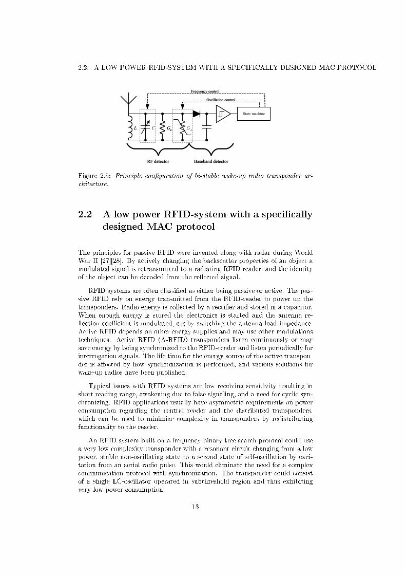
Figure 2.5: Principle conguration of bi-stable wake-up radio transponder ar-chitecture.
2.2 A low power RFID-system with a specically
designed MAC protocol
The principles for passive RFID were invented along with radar during WorldWar II [27][28]. By actively changing the backscatter properties of an object amodulated signal is retransmitted to a radiating RFID reader, and the identityof the object can be decoded from the reected signal.
RFID systems are often classied as either being passive or active. The pas-sive RFID rely on energy transmitted from the RFID-reader to power up thetransponders. Radio energy is collected by a rectier and stored in a capacitor.When enough energy is stored the electronics is started and the antenna re-ection coecient is modulated, e.g by switching the antenna load impedance.Active RFID depends on other energy supplies and may use other modulationstechniques. Active RFID (A-RFID) transponders listen continuously or maysave energy by being synchronized to the RFID-reader and listen periodically forinterrogation signals. The life time for the energy source of the active transpon-der is aected by how synchronization is performed, and various solutions forwake-up radios have been published.
Typical issues with RFID systems are low receiving sensitivity resulting inshort reading range, awakening due to false signaling, and a need for cyclic syn-chronizing. RFID applications usually have asymmetric requirements on powerconsumption regarding the central reader and the distributed transponders,which can be used to minimize complexity in transponders by redistributingfunctionality to the reader.
An RFID system built on a frequency binary tree search protocol could usea very low complexity transponder with a resonant circuit changing from a lowpower, stable non-oscillating state to a second state of self-oscillation by exci-tation from an aerial radio pulse. This would eliminate the need for a complexcommunication protocol with synchronization. The transponder could consistof a single LC-oscillator operated in subthreshold region and thus exhibitingvery low power consumption.
13

CHAPTER 2. LOW POWER SHORT RANGE RADIO COMMUNICATION
Figure 2.6: Frequency spectrum allocation used by the communication protocol.
2.2.1 Principle of operation
In this RFID system an LC-oscillator, see Figure 2.5, is used in the transponderas a wake-up radio. The oscillator is designed to consume low power by oper-ating in the weak inversion region (subthreshold). The oscillator is biased nearoscillation and a radio signal received by the antenna pushes the bias point intoa region where stable oscillation is obtained, resulting in a signal being trans-mitted back (backscattered) to the reader on the same frequency. These arethe two intended states of operation for the receiver, the idle state, where thereceiver is armed and waiting for an input signal, and the active state, in whichit has received an input signal and therefore is oscillating. The idle state corre-sponds to a bias point with lower loop gain, and the active state corresponds toa bias point with higher loop gain. The nonlinear response is essential for theability to achieve stability in each of the described states. The necessary energyin the incoming pulse that may change state of the receiver depends on thenonlinearity of the active device, as well as on the Q-value of the tank circuit.
The protocol for communication between the transponder and reader is de-scribed in [29] and is of the binary tree type, meaning that the ID is extractedbit by bit when traversing a binary tree detecting whether the transponder'snext ID-bit is a '0' or a '1'.
To extract bits in the transponder ID, the protocol uses frequency signaling.The transponders in the vicinity of the reader are rst awakened by a beaconsignal. The awakened transponders IDs are extracted by using four dierentfrequencies, where every frequency corresponds to a two-bit combination in theID as follows and is spread in the 2.45 GHz ISM band, see Figure 2.6.
f0: is the beacon signal, 2400+n0 [MHz], used to wake up all transponderswithin the reader's range
f1: '00msb', 2400+n0+n1 [MHz]
f2: '10msb', 2400+n0+n1+n2 [MHz]
f3: '01msb', 2400+n0+n1+n2+n3 [MHz]
f4: '11msb', 2400+n0+n1+n2+n3+n4 [MHz]
It is possible to identify all transponders in range for the reader withoutknowing anything in advance of the transponder population. The ID extraction
14

2.2. A LOW POWER RFID-SYSTEM WITH A SPECIFICALLY DESIGNED MAC PROTOCOL
Table 2.1: System components data used for evaluation of communication pro-tocol.
Transponder power consumption, idle state [mW] 0.02Tag power consumption, active state [mW] 1.4Tag sensitivity [dBm] -72Tag output power [dBm] -10Tag idle to active state [µs] 1.0Reader sensitivity [dBm] -85Reader output power [dBm] 20
starts when the reader transmits the beacon signal (on frequency, f0), awakeningall transponders in reach. In the next step the reader transmits on all fourfrequencies, f1f4, simultaneously. A transponder is initially "tuned" to thefrequency corresponding to its two least signicant ID bits, and the transpondertransmits back, only, when receiving a signal at its "tuned" frequency. Thismethod is iterated, traversing bit by bit, halving the transponder population.When the last bits are read one branch is nished, and next may be followed.
In some applications it is known which transponders that should be in vicin-ity of the reader. Instead of trying to read all transponders it is possible toselectively read transponders. If the ID of a transponder is already known bythe reader, then it is possible to address that specic transponder. The readeruses the frequency "trail", which is composed of the bit combination in thetransponder ID in a straightforward way. The addressing method is useful forsaving transponder energy, only doing a minimal number of activations of thetransponders.
2.2.2 Results and discussion
The proposed low power detector is listening without a running LO. It is inconstant operation without duty cycling, thus enabling a short response time.However, the sensitivity to biasing conditions is clear in both measurements andsimulations. Measurements on a low frequency prototype show that the circuitis fairly stable over time with a slight drift in the tens of millivolts range for thebias voltage keeping the circuit in idle state. A basic detector model predictsthe sensitivity bandwidth to be controlled by the bias of the active elements,which is also conrmed by measurements.
False triggering may drain the power supply and must be minimized. Apartfrom using calibration strategies, this should also be handled at the higherprotocol level. As an example, frequency hopping technique will be used, whereeach hop has the potential to trigger the receiver oscillations [29]. It follows thatit is important to minimize the number of frequency hops used for addressingeach single transponder.
The results from the simulations are presented as 1) read-out delay, the timeit takes in average to read a transponder ID, and 2) the tag life time whendraining the tag battery. Calculations are based on numbers in Table 2.1. Allsimulations have been made with the detector biased 1 mV below the level wherethe self induced oscillation starts.
The calculated expected life time of how many days a battery will last if the
15

CHAPTER 2. LOW POWER SHORT RANGE RADIO COMMUNICATION
30 40 50 60 70 80 90 1000
50
100
150
Q
P DC [
μW]
Power consumption
Z
0=2000 Ω
Z0=1000 Ω
Z0=500 Ω
Figure 2.7: Simulated power consumption for the wake-up transponder depictedin Fig. 2.5 in its idle state for dierent inductor Q-values and interfacingRF-port impedances (Z0). With inductance L = 5.216 nH, transistor widthW=175 µm (making up GA), and at fc=2.5 GHz.
reader tries to read the transponders every 60 seconds is more than 900 days.The maximum throughput is 1570 transponders per second.
More than 1500 transponders can be read per second with the system. Theaverage delay when reading a transponder ID in a population of 1000 transpon-ders is 319 ms.
The theoretical reading range in free space is 50 meters. The estimatedlife time for a transponder, in this active RFID system, powered by a low-cost7x7 square centimeter printed battery is almost three years. This is in a scenariowhere the transponder's ID is read out as often as 60 times per hour and onlyconsidering the energy content in the battery.
A matter of importance is the dierence between nal oscillation and thesensitivity center frequency of the detector. This will have an impact on howthe detector may be used. If we want the detector to work as a backscattererthis dierence must be incorporated in the communication protocol, otherwisethe oscillation frequency has to be tuned during the transmitting period. In anycase the current through the detector will increase and the incoming signal isdetected.
The power consumption is as expected lowest for the implementation witha combination of high impedance and high Q-value. Further, the lowest currentand power is found with the largest inductor, which in turn results in the smallesttransistor. The variation in power consumption is seen in Fig. 2.7.
Wake-up radios not being based on duty cycling make each transponderreachable by the RFID reader at any time and do not need any advanced
16

2.3. A LOW POWER OSCILLATOR-FREE CMOS TRF RECEIVER
synchronized wake-up algorithms. Reducing complexity of transponders infersa corresponding increase in reader complexity. The low complexity and lowpower consumption of the described backscatter radio transceiver enable low-cost transponders with long reading range and two-way communication betweentransponder and reader.
The principle of the transponder operation was proven with a discrete lowfrequency prototype. The discrete implementation may be transferred to amonolithic design performing at higher frequencies. Simulations of a monolithicimplementation using 180 nm CMOS transistors were performed at 2.5 GHz.In simulations the power consumption for the detector is below 125 µW at asensitivity of -83 dBm and a bandwidth of 9 MHz.
However, the simple analog hardware solution come at the cost of need forcalibration to keep the transceiver in its stable state. Keeping the conductanceG = GL −GA as stable as possible is essential for the system. The importantparameter here is the active device transconductance which is controlled by thebias current. The transconductance of a MOS device biased in the subthresholdregion has an exponential temperature dependence. Several strategies are pos-sible, one suggestion being self calibration with the potential to mitigate bothfabrication and temperature variations. The calibration may be performed as abinary process homing in on the bias point just below noise induced self oscil-lation, a similar method is described in [30].
A more robust solution would be preferable, and given the complicationsassociated with the bistable transceiver it is plausible to compare the bistabletransceiver with a oscillator-free TRF receiver. The TRF receiver may initializeany transmitter on wake-up and thus form a complete transceiver if needed. Animportant argument for looking into the TRF receiver is that it is well suitedfor implementation in an ordinary CMOS process.
2.3 A low power oscillator-free CMOS TRF re-
ceiver
A TRF receiver performs envelope detection at the carrier frequency withoutany prior frequency conversion. Thus energy consuming oscillators and mixersare avoided, but at the cost of sensitivity and selectivity. In the TRF receiverselectivity is achieved by a preceding RF-lter. The receiver presented below isa TRF receiver without oscillators, neither in the RF chain nor in the basebandstages. No external components are used, except for a transmission line voltagetransformer on the FR4 laminate carrying the RF-ASIC.
2.3.1 Description of the receiver architecture
A Wake-up radio has the single purpose to recognize a predetermined ID-codebit pattern in the air, and the chosen architecture is focused on simplicity. Ituses no superregenerative solutions or oscillators, and no control or calibrationloops such as phase locked loops. This enables a short startup time and avoidany lock-in processes adding to overall power consumption [13].
As much as possible of the radio functionality should be handled over to theinterrogator or reader (the term "reader" emanates from the RFID communityand is a bit misleading here since we only use downlink communication). A very
17

CHAPTER 2. LOW POWER SHORT RANGE RADIO COMMUNICATION
ID code
Envelope Detector
Figure 2.8: Block diagram of low-power oscillator-free CMOS TRF receiver.
fmfrequency
f0 f0+fmf0-fm
fmfrequency
f0 fbf0+fmf0-fm
Figure 2.9: Frequency translation by envelope detection of an ASK-modulatedsignal.
limited amount of data will be sent at each wake up session, only a few hundredbits containing an ID-code. We use OOK modulation of the carrier; althoughthis is spectral inecient it is motivated by the short transmission bursts andthe simplication of the receiver design. A carrier frequency of 2450 MHz (ISM)oers a good compromise between size and range, and an ability to see "around"corners and obstacles. The overall receiver block diagram is found in Fig.2.8.
Envelope detector
The incoming RF carrier drives a diode, or other rectifying component. Theenvelope detector self mixing eciency falls o as the carrier power decrease.Thus the sensitivity for a TRF receiver is moderate compared to the superheterodyne with a mixer always being eciently switched by a strong LO sig-nal. However, the typical applications for Wake-up receivers require only rathershort transmission range, up to about 10 meters [31]. Excluding the LO is wellmotivated by the achieved reduction in active power.
The envelope detector folds the modulated spectrum around the carrier f0
down to baseband frequency fm, see Fig. 2.9. The baseband output voltage Vmfrom the envelope detector is proportional to the square of the input amplitudeof the RF carrier VRF ,
Vm ∝ V 2RF . (2.1)
Boosting VRF with a pre-amplier in front of the detector would improve thesensitivity. It is worth to note that it is the carrier amplitude that is impor-tant, rather than carrier power, and that voltage amplication can be achievedpassively by a transformer. It is dicult to get ecient voltage transformationwith on-chip inductors, the large inductance needed would occupy large die area
18
2.3. A LOW POWER OSCILLATOR-FREE CMOS TRF RECEIVER
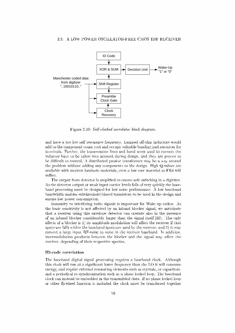
Clock Recovery
Shift Register
ID Code
XOR & SUM
Manchester coded datafrom digitizer”..10010110..”
Decision UnitWake-Up”1" or ”0”
PreambleClock Gate
Figure 2.10: Self-clocked correlator block diagram.
and have a too low self resonance frequency. Lumped o-chip inductors wouldadd to the component count cost and occupy valuable bonding pad resources forterminals. Further, the transmission lines and bond wires used to connect theinductor have to be taken into account during design, and they are proven tobe dicult to control. A distributed passive transformer may be a way aroundthe problem without adding any components to the design. High Q-values areavailable with modern laminate materials, even a low cost material as FR4 willsuce.
The output from detector is amplied to ensure safe switching in a digitizer.As the detector output at weak input carrier levels falls of very quickly the base-band processing must be designed for low noise performance. A low basebandbandwidth enables subthreshold biased transistors to be used in the design andensure low power consumption.
Immunity to interfering radio signals is important for Wake-up radios. Asthe basic sensitivity is not aected by an inband blocker signal, we anticipatethat a receiver using this envelope detector can operate also in the presenceof an inband blocker considerably larger than the signal itself [32]. The onlyeects of a blocker is 1) its amplitude modulation will aect the receiver if thatspectrum falls within the baseband spectrum used by the receiver, and 2) it mayconvert a large input RF-noise to noise in the receiver baseband. In addition,intermodulation products between the blocker and the signal may aect thereceiver, depending of their respective spectra.
ID-code correlation
The baseband digital signal processing requires a baseband clock. Althoughthis clock will run at a signicant lower frequency than the LO it will consumeenergy, and require external resonating elements such as crystals, or capacitors,and a periodical re-synchronization such as a phase locked loop. The basebandclock can instead be embedded in the transmitted data. If no phase locked loopor other ywheel function is included the clock must be transferred together
19

CHAPTER 2. LOW POWER SHORT RANGE RADIO COMMUNICATION
in
A
g
Figure 2.11: Layout of the RF voltage transformer metal pattern on PCB.
with each data bit. Manchester coding enables this by coding each ID-code bitwith a transition; the bit value "1" is coded with a "01"-transition, and bit value"0" is coded with a "10"-transition [33]. The cost is a doubled edge rate butthe gain is, again, a simplied design. The actual bandwidth of the basebandsignal is not increased but shifted upwards, reducing the impact of 1/f-noise[34]. Further, the baseband signal will be DC-free and the baseband circuitrywould not need to have any DC-gain. DC level uctuations from the detectorare blocked out from the baseband amplier by a DC-block capacitor.
A self clocked correlator, see Fig. 2.10, compares the received data withthe stored ID. Data would be shifted in to a shift register by the recoveredclock encoded in the Manchester data. A short preamble bit pattern is used totrigger the clock recovery circuit to start up. This would reduce the activityof the digital logic and save spending of dynamic energy. The length of theID-code typically is around 100 bits. The EPC transponder Class 3 use 96 bits[35]. After Manchester encoding and addition of preamble the result is around200 bits to transfer over the air interface. One thousand units may be addressedwithin one second with a bit rate of 200 kbps.
RF voltage transformer
An RF voltage transformer was placed on the same FR4 PCB carrying the die.The matching network was designed for a 0.508 mm thick FR4 laminate, seeFig. 2.11, and consisted of a 50 Ω transmission line leading to a single stubcombined with a transmission line. Further, a bias network (not depicted inFig. 2.11) for biasing of the detector via the RF input pad was attached to thetransformer.
If a planar antenna (e.g. integrated to the carrier substrate) is used, itsimpedance is likely to dier from 50 Ω. That is not a major concern, it merelycalls for a dierent design of the matching network.
Baseband amplier
Baseband amplication was performed by two cascoded ampliers with feedbackconnected in series, see Fig. 2.12.
The detector signal is very weak and we do not want the baseband amplierto dominate the noise budget. Therefore the baseband ampliers have to be
20

2.3. A LOW POWER OSCILLATOR-FREE CMOS TRF RECEIVER
VA
Vin
M3
M1
Cdeco
VA
Vref
M4
M2
M9
Ibias,ref
M5
M7
M6
M8
VB VB
Rf
Ci
M10
VA M13
M11
Cdeco
VA
Vref
M14
M12
M19
Vout
M15
M17
M16
M18
VB VB
Figure 2.12: Schematics for baseband amplier with bandpass characteristics.
designed for low noise performance. The largest noise contributor is the inputtransistor M1 of the rst amplier stage.
The lter topology chosen have a bandpass characteristic and requires ahigh resistive path, Rf , and a DC-blocking capacitor Ci. The high resistancein the feedback ensures a high input impedance towards the detector. Theresistor Rf is set to 65 MΩ, and is implemented with the channel resistance ofa subthreshold biased MOST.
A source follower amplier (not depicted in Fig. 2.12) was added to thedesign as buer for measurement purposes. The buer amplier adds no voltagegain but is capable to drive larger currents and isolates the baseband amplierfrom the capacitive and resistive loading of the bonding pad and measurementequipment.
2.3.2 Results and discussion
The receiver was fabricated in a 130 nm CMOS process with MIM capacitors.No external components were used other than an etched transformer in the FR4carrier PCB. The integrated circuitry, see Fig. 2.13, was tted within an area ofaround 7000 µm2 and is hence suited to be used as an IP-block being placed ina die corner, or near the die edge, of a general ASIC. The receiver was designedfor 1V bias to enable a low power design. For the same purpose all devices areoperating in moderate or weak inversion. The total current consumption of thedetector and baseband amplier is 2.3 µA.
The receiver sensitivity was measured with a 2450 MHz carrier signal modu-lated with 100% ASK. The best sensitivity, Pin=-48.5 dBm, is found at fin=2520 MHz,which corresponds to the best matching response from the transformer.
The proposed design is very resilient to interfering sources with a modula-tion spectrum outside the baseband amplier bandwidth. Further, the use ofa passive transformer for amplication makes the design robust against satura-
21

CHAPTER 2. LOW POWER SHORT RANGE RADIO COMMUNICATION
Figure 2.13: Die photo of WuR implemented in a CMOS 130nm process andmounted on FR4 carrier substrate.
2200 2300 2400 2500 2600 2700 2800
-55
-50
-45
-40
fblocker
[MHz]
Pbl
ocke
r [dB
m]
Blocker immunity BER<10-3
Pin
=-44.5dBm fin
=2450MHz
50kHz square wave 100% ASK90kHz square wave 100% ASK
Figure 2.14: Measured immunity to modulated blocker signal.
22
2.3. A LOW POWER OSCILLATOR-FREE CMOS TRF RECEIVER
2200 2300 2400 2500 2600 2700 2800-65
-60
-55
-50
-45
-40
-35
fblocker
[MHz]
Pbl
ocke
r [dB
m]
Broadband blocker (5MHz) immunity BER<10-3
Pin
=-44.5dBm fin
=2450MHz
Figure 2.15: Measured immunity to broadband 64QAM modulated blocker signal(simulating WLAN).
tion and signal intermodulation caused by any overdrive of active components.A CW blocker signal with a level of -13 dBm only 1 MHz below the carrierdid not swamp the sensitivity of the radio. During these measurements themodulated carrier signal, at 2450 MHz, was xed at a power 3 dB above therequired level for a BER=10−3 without interference. Interestingly the sensitiv-ity can be improved by a CW interferer, and a sensitivity of Pin=-57.5 dBmwas measured with a -20 dBm CW blocker 1 MHz below the carrier frequency.This improvement falls o rapidly as the blocker frequency moves out from thecarrier frequency, and the receiver is virtually unaected.
The result from the same set up, but with a modulated blocker, is presentedin Fig. 2.14. As long as the modulated interferer power was roughly 6 dB belowthe sensitivity limit level the Wake-up radio was not blocked.
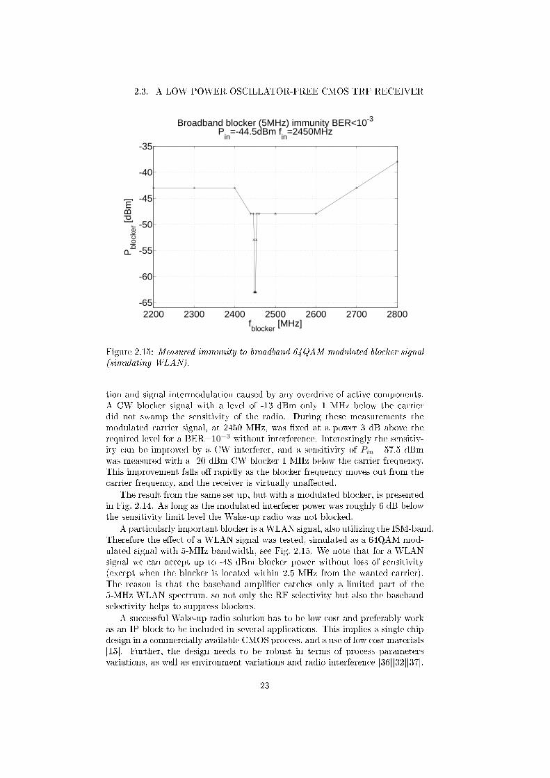
A particularly important blocker is a WLAN signal, also utilizing the ISM-band.Therefore the eect of a WLAN signal was tested, simulated as a 64QAM mod-ulated signal with 5-MHz bandwidth, see Fig. 2.15. We note that for a WLANsignal we can accept up to -48 dBm blocker power without loss of sensitivity(except when the blocker is located within 2.5 MHz from the wanted carrier).The reason is that the baseband amplier catches only a limited part of the5-MHz WLAN spectrum, so not only the RF selectivity but also the basebandselectivity helps to suppress blockers.
A successful Wake-up radio solution has to be low cost and preferably workas an IP block to be included in several applications. This implies a single chipdesign in a commercially available CMOS process, and a use of low cost materials[15]. Further, the design needs to be robust in terms of process parametersvariations, as well as environment variations and radio interference [36][32][37].
23

CHAPTER 2. LOW POWER SHORT RANGE RADIO COMMUNICATION
The presented design oers a robust and trim-free solution easily implementedin a CMOS process.
The implementation of low-power TRF receivers requires many and compli-cated trade-os, and the question remains if it is possible to push the receiverenergy eciency even further? A structured analysis of the lower bound forWake-up receivers energy consumption would be a valuable support for design-ers of modern radio systems.
2.4 Analysis of lower bound for WuR energy con-
sumption
In the survey presented in Fig. 2.4 a lower bound for the attainable energy con-sumption per received bit is discernible, but what is the fundamental reasonfor this bound? Among the requirements driving power consumption are base-band bandwidth, sensitivity, and also carrier frequency and interference [32]. Bystudying basic receiver circuits it is possible to provide an overview of the rsttwo of these mentioned requirements (baseband bandwidth and sensitivity) andto provide an intuitive picture of their relations to power consumption. The TRFreceiver, with and without a preceding LNA, and the superheterodyne receiverare treated in the following analysis. The regenerative and super-regenerativereceiver will not be analyzed analytically here, but are included in the surveypresented in Fig. 2.4.
2.4.1 Description of parameter set and analysis
Noise in a linear system may be calculated with Friis cascade formula for noisegure F ,
F = F1 +∑j
Fj − 1∏i<j G
2i
, (2.2)
where Fj and Gi is the noise gure and voltage gain respectively for each stagein the cascaded system. The assumption of linearity is valid for most receiverbuilding blocks at low power signal levels, with the detector as an exception.Analysis for the envelope detector (ideal squarer) can be found in [32], [38].
For the analysis it is necessary to choose reasonable parameter values. Thesevalues may be updated as technology development continues. The componentvalues, or the parameter set, used in the following is meant to reect typicalvalues for integrated CMOS fabrication processes, and typical small sized RFlumped components. Normally the number of discrete components is a strongdriver of cost, so we look for single chip solutions with a minimum numberof external components. The minimum output SNR for reliable detection isassumed to be 12 dB [15].
90nm CMOS is chosen as reference technology, using the same basic pa-rameters as in [39] (Cmin = 1 fF and eective voltage V0 = 75 mV). On-chipinductors rarely reach higher inductance values than 10 nH or a better Q than5 [22]. Further, the loading capacitance of an ASIC bond pad end up at around400 fF when ESD protection is included. Here it is assumed that we may reducethe load to 75 fF, reecting the ongoing development of RF ESD clamps [40].
24

2.4. ANALYSIS OF LOWER BOUND FOR WUR ENERGY CONSUMPTION
(·)2
fRF fBB
out
VRF VD VBB VcmpfRF
BRF BBB
in
RF Detector Baseband
fBB
Figure 2.16: Tuned RF receiver (TRF). Signal-to-noise ratio is symbolized withη
VD
Id2
2
Cd
is+indRf
ina
Vcmp
3
Id3CDC
Figure 2.17: RF-detector and transimpedance amplier (TIA).
External inductors display a Q of around 35 for inductance values available witha serial resonance above the carrier frequency we look into. Further the base-band noise bandwidth BBB is assumed to be twice the bit rate of the receiver(i.e. the bit rate 250 kbps require a baseband bandwidth of BBB = 500 kHz).Furthermore the temperature is assumed to be T = 300 K. Finally, a supplyvoltage of 1 V is used in the analyzed designs. Supply voltage may be as low as0.5 V, but it will not change the conclusions.
Tuned RF receiver
A block schematic of a TRF receiver is found in Fig. 2.16. In the TRF thereceived signal is bandpass ltered around the intended RF center frequency,fRF , with a bandwidth BRF to reduce impact from out of band interfering sig-nals. The RF-lter of a Wake-up radio usually is broadband, to make it robustagainst process variations and to add a minimum of loss. The antenna itselfis likely to be resonant and may provide sucient selectivity. The inclusion ofan RF pre-amplier is optional, and depend on the targeted receiver sensitivity.Amplication of the signal before detection increases the sensitivity, but has asubstantial impact on the power budget since RF gain is expensive from a powerperspective.
The most basic implementation of the TRF is an envelope detector followedby a baseband amplier, see Fig. 2.17. Basically this is an integrated versionof the vintage crystal radio, where the incoming radio signal voltage VD drivesa detector transistor M2 instead of a crystal diode. The outgoing detectorcurrent is is ltered by a detector capacitor Cd before being amplied in atransimpedance amplier consisting of transistor M3 and feedback resistor Rf .Capacitor Cd also acts as a low impedance path to ground for the radio signal.
25

CHAPTER 2. LOW POWER SHORT RANGE RADIO COMMUNICATION
VRF
RA RS
Figure 2.18: RF-transformer with input impedance RA and output impedanceRS and passive voltage gain GT =
√RS/RA. The transformer also works as a
matching network and a lter
RA
LT
Cpad
VRF
rT
2VA
Figure 2.19: RF-transformer with external inductor in series with the capaci-tance of the chip RF input port
Noise from the detector is represented by the current ind, while amplier noiseis represented by the current ina. The outgoing voltage Vcmp is digitized in acomparator, or by an ADC. Bias currents for the transistors are Id2 and Id3.
With an up-transforming network between the antenna and the detector thesensitivity is improved. A passive up-transformer works by trading current forvoltage amplitude and thus increases the (usually) low antenna impedance, RA,to a higher value, RS , see Fig. 2.18. With a suciently small detector transistorthe MOS gate input impedance will be high and the achievable transformationratio will rather be limited by the Q-value of the resonating elements. This isillustrated with the straightforward impedance transformer circuit consisting ofan external inductor in series with the chip RF input port, see Fig. 2.19. Theexternal inductor with inductance LT has a nite Q represented by a seriesresistance rT . Matching is achieved at resonance if we choose rT to be equalto antenna resistance RA. The voltage at the chip input is VRF = QVA, andthe passive voltage gain becomes GT = Q. With an RF port pad capacitanceCpad = 75 fF and a target resonance frequency of 2.5 GHz the inductanceLT becomes 54 nH. Now, with an antenna impedance of 50 Ω the inductor Qequates to roughly half the assumed achievable value of 35 in our parameter set.However, this is readily solved by reducing the antenna impedance by a factorof two since small sized antennas in any case are known to have a low radiationresistance [41], thus leading to antenna impedance RA = 25 Ω and a Q of 35.
We obtain the following expression for outgoing SNR of the TRF withoutLNA,
ηout =
(Id2V
2D/(4V
20 ))2
4γkTBBBId2/V0 +16π2kTγC2
dB3BB
3Id3/V0
, (2.3)
26

2.4. ANALYSIS OF LOWER BOUND FOR WUR ENERGY CONSUMPTION
where V0 is the ecient voltage of the transistors and k is Boltzmanns constant.The transistor noise parameter γ is henceforth approximated with γ = 1, forbetter readability of expressions.
The optimum distribution of the two bias currents Id2 and Id3 in this re-ceiver depends on targeted sensitivity, and the relation may actually be betterperceived if we instead look at the inverse of (2.3),
1/ηout =64kTBBBV
40
V 4D
(1
Id2V0+
4π2C2dB
2BBV0
3Id3I2d2
). (2.4)
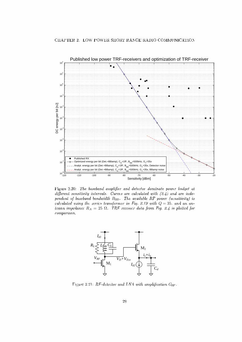
Here two terms are being functions of the bias currents, each term dominatethe SNR calculation within dierent intervals of sensitivity. The goal for adesigner is to nd a distribution of bias currents with minimum total current,Itot = Id2 + Id3, while still passing the SNR threshold resulting in a BER=10−3.If we look at the two terms in (2.4) isolated one at a time, the expected behaviorof an overall optimization may be foreseen. The rst term of (2.4), dominatesthe power budget for higher sensitivities, and is plotted as energy-per-bit inFig. 2.20 with the total bias current going through the detector (Id2 = Itot).In this domain detector noise is prevailing, and DC-power should be spent ondetector biasing. The RF sensitivity in Fig. 2.20 is calculated with GT = 35and RA = 25 Ω. The second term of (2.4) dominates the power budget at lowsensitivities, and it can be showed that this term is minimized when Id3 = Itot/3.In Fig. 2.20 the second term is plotted as energy-per-bit with this optimizedcurrent distribution. In this domain the baseband amplier noise prevails andthus the DC-power should be diverted from the detector to the baseband chaininstead.
This is also an expected result from (2.2) where the noise gure of the rststage, if having enough gain, will dominate the overall system noise gure.
The overall power optimization of the receiver is graphically presented inFig. 2.20. The optimized curve makes a smooth transition between the twosensitivity intervals.
The energy-per-bit for the TRF receiver without LNA is independent ofbaseband bandwidth. When the rst term in (2.4) dominates SNR, ηout isproportional to Itot/BBB (energy-per-bit). With the second term dominatingηout is proportional to (Itot/BBB)3 (the cube of energy-per-bit).
Boosting VRF with a pre-amplier, beyond what is possible with a passiveimpedance transformer, would improve the receiver sensitivity drastically. How-ever, it is not obvious at what level of sensitivity the pre-amplier pays o inour power budget.
In Fig. 2.21 a TRF with LNA is depicted. The baseband amplier is hereskipped for simplicity. LNA noise is represented by the voltage VD,n, whileoutgoing noise from the detector is represented by in.
The LNA has a resonant load providing narrow band amplication at acarrier angular frequency ωRF = 2πfRF , and thus also oer some RF ltering.The expression for the RF gain with a resonant load having quality factor QLis,
GRF = gm1RL =gm1QLωRFCL1
, (2.5)
where gm1 is the transconductance, RL is the load impedance, and CL1 is thecapacitive load from subsequent stages and possible tuning capacitors.
27
CHAPTER 2. LOW POWER SHORT RANGE RADIO COMMUNICATION
-120 -110 -100 -90 -80 -70 -60 -50 -40 -30 -2010
-8
10-7
10-6
10-5
10-4
10-3
10-2
10-1
100
101
102
Sensitivity [dBm]
DC
ene
rgy
per
bit [
nJ]
Published low power TRF-receivers and optimization of TRF-receiver
Published RXOptimized energy per bit (Det.+BBamp), C
D=1fF, B
BB=500kHz, G
T=35x
Analyt. energy per bit (Det.+BBamp), CD=1fF, B
BB=500kHz, G
T=35x, Detector noise
Analyt. energy per bit (Det.+BBamp), CD=1fF, B
BB=500kHz, G
T=35x, BBamp noise
Figure 2.20: The baseband amplier and detector dominate power budget atdierent sensitivity intervals. Curves are calculated with (2.4) and are inde-pendent of baseband bandwidth BBB. The available RF power (sensitivity) iscalculated using the series transformer in Fig. 2.19 with Q = 35, and an an-tenna impedance RA = 25 Ω. TRF receiver data from Fig. 2.4 is plotted forcomparison.
Id2
2
Cd
is+in
1
Id1
VRF VD+VD,n
RL CLL
Figure 2.21: RF-detector and LNA with amplication GRF .
28
2.4. ANALYSIS OF LOWER BOUND FOR WUR ENERGY CONSUMPTION
The expression for output SNR (again inverted) of the complete TRF re-ceiver with the LNA included and as a function of biasing currents is,
1/ηout =32kTBBBV 2RF
(2V 7
0 (ωRFCL1)4
Id2I4d1V
2RFQ
4L
+V0
Id1
). (2.6)
We identify two dierent terms dominating the power budget at dierent sensi-tivity intervals. With typical on-chip low Q inductors and for reasonable sensi-tivities the rst term, representing detector noise, will dominate over the secondterm, representing converted noise from the LNA transistor M1. It can be shownthat the bias current distribution that minimizes the rst term is Id1 = 4/5Itot,where Itot = Id1 + Id2. The result depends on the baseband bandwidth in thiscase. The improvement with an LNA is signicant for higher sensitivities, whileat lower sensitivities the LNA becomes superuous. The sensitivity level wherethe pre-amplier pays o depend on targeted bandwidth (i.e. bit rate).
With a resonant load the amplier performance is limited by the inductanceand the Q-value that is possible to achieve with on-chip inductors. The achiev-able inductance also imposes a lower limit on the capacitive load if resonanceshould be attained. If we instead look at a pure resistive load the capacitancecan be minimized CL1 = Cmin. We can now easily modify (2.6) with Q set tounity,
GRF = gm1RL =gm1
ωRFCL1, (2.7)
where we have used the bandwidth requirement RL = 1/(ωRFCL1) limiting theload resistor size [39]. We get,
1/ηout =32kTBBBV 2RF
(2V 7
0 (ωRFCmin)4
Id2I4d1V
2RF
+V0
Id1
). (2.8)
If we have the opportunity to place the inductance of the resonant LNAoutside the chip, some advantages can be noted. First, we may increase theinductance value, giving a higher load impedance. Second, the Q of an externalinductor is normally better due to larger size and a better isolation from lossysubstrate material. However, we also note some complications with this proce-dure. The typical bond pad parasitic capacitance limits the size of applicableinductors (since resonance frequency of the amplier load is ω0 = 1/
√LC). Fur-
ther, the process of bonding and contacting external components complicatesthe implementation and make it technically challenging.
We conclude that the overall power consumption is reduced with the higherQ oered by an external inductor, and that the LNA continues to contributeto reduction of power down to lower sensitivities. However, we also note thatan external inductance can not compete with the performance of a cheaper andtechnically less complicated on-chip resistive load, see Fig. 2.24.
It is here relevant to mention active inductors as an alternative to passiveinductors. The voltage gain of an LNA with an active inductor, see Fig. 2.22,with transconductance gm and a capacitive load CL, can be shown to be AV =(gm/(ωCL))2. If we look for a voltage gain of say AV =10, this corresponds to atransconductance of 50 µS with the minimum capacitance Cmin at the frequency2.5 GHz. A resistive load requires a
√AV =
√10 times larger conductance under
the same conditions, equating to 157 µS. Taking into account the added noise
29

CHAPTER 2. LOW POWER SHORT RANGE RADIO COMMUNICATION
Vin
ML
MXCL
RF
Cg
iL
VL
+
_
Vout
Figure 2.22: Amplier with active inductive load.
Antenna
fLO
(·)2
RFBRF
DetectorIF Baseband
out
VcmpfBB
VRF
fRF
in
VD
fIFVBB
fBB
BIF BBB
Figure 2.23: Superheterodyne receiver (SHET).
associated with active inductors the net improvement is rather small. The use ofan external inductance with Q =35 resonating together with a pad-capacitanceof 75 fF would require a transconductance of 337 µS to achieve the same gain.
Superheterodyne receiver
One of the most widely used radio receiver architectures is the superheterodyne,depicted in Fig. 2.23. It diers from the TRF by a down-converting stage thatreduces signal frequency before the actual detection take place. Among theprimacies of the superheterodyne we nd a high sensitivity and well controlledchannel ltering. Further, the amplication at the IF require less DC-power.On the other hand, the down-converting mixer stage needs to be driven by aLO that constantly drains the power supply. The superheterodyne receiver maybe tuned to dierent RF channels by shifting the LO frequency. A negativeconsequence of this tuning ability is that the superheterodyne is sensitive toLO frequency instabilities, but this problem can be mitigated by using a moretolerant IF-stage design [15].
We have studied oscillator realizations using an RC-tank circuit and LC-tankcircuits. RC-oscillators have the advantage over LC-oscillators of being easier tointegrate on chip since they have no large inductor consuming expensive siliconarea. One major drawback is that the lossy RC-network implies a higher powerconsumption and lower Q leading to increased phase noise as compared to anLC-oscillator. Although ASK modulation is not phase sensitive, the phase noiseof the LO may reduce SNR by converting adjacent channel interferers into thebaseband [42]. An overview of the oscillator bias currents is found in Table 2.2.
30

2.4. ANALYSIS OF LOWER BOUND FOR WUR ENERGY CONSUMPTION
Table 2.2: Estimated critical currents for oscillator implementationsImplementation Resonant tank parameters Icrit [µA]LC on-chip C = 400 fF, L = 10 nH, Q = 5 637RC on-chip C =1 fF, R = 63.7 kΩ 23.6LC o-chip C = 75 fF, L = 54 nH, Q = 35 16.8
-120 -110 -100 -90 -80 -70 -60 -50 -40 -30 -2010
-7
10-6
10-5
10-4
10-3
10-2
10-1
100
101
102
103
Sensitivity [dBm]
DC
ene
rgy
per
bit
[nJ]
Published low-power receivers and optimization of superhet. with LNA
Published RXOptimized LNA, IFamp, and Det., f
IF=250MHz G
T=35x [LO on-chip L] I
LO=637uA
Optimized LNA, IFamp, and Det., fIF
=250MHz GT=35x [LO on-chip RC] I
LO=23.6uA
Optimized LNA, IFamp, and Det., fIF
=250MHz GT=35x [LO off-chip L] I
LO=16.8uA
Analyt. LNA and Det., QL=5, L=10nH, B
BB=500kHz, G
T=35x, Det. noise
Analyt. LNA and Det., QL=35, C
L=75fF, B
BB=500kHz, G
T=35x, Det. noise
Analyt. LNA and Det., CL=1fF, R
L=(
RFC
L)-1, B
BB=500kHz, G
T=35x, Det. noise
Estimated lower bound for BBB
=500kHz
Figure 2.24: The red dotted line is the best estimate of the lower bound to powerconsumption at baseband bandwidth BBB=500 kHz for any receiver architecture(the line stops at the antenna noise limit). Data for all receivers from Fig. 2.4is plotted for comparison. Energy-per-bit for the superheterodyne with LNA(triangles). The impact of the mixer noise is reduced by the use of an LNA.The LO supply power add a lower oor on energy-per-bit performance at lowsensitivities. With wider baseband bandwidths, BBB, this oor will be pusheddownwards. Other lines show energy-per-bit for TRF with preceding LNA usingdierent loads.
31

CHAPTER 2. LOW POWER SHORT RANGE RADIO COMMUNICATION
2.4.2 Results and discussion
The above analysis does not take into consideration the use of cascade amplierstages. An amplier block may consist of multiple K + 1 stages in a chain,where gain factors are multiplied and bias currents are summed. Only therst stage in the cascade has to be optimized for noise, with say a currentIdn. Subsequent stages may instead be optimized for maximum gain. If weassume equal amplication in each subsequent stage of the cascade, and eachstage has a gain proportional to their individual bias current Idk, then the totalamplication of the subsequent cascade is proportional to IKdk and the total biascurrent is Id = KIdk. If we modify our expressions for gain according to thiswe have,
G =IdnV0
RLIKdkV K0
RKL =IdnI
KdkR
(K+1)L
V K+10
(2.9)
This extension of our analysis would result in somewhat lower bounds but willnot change our general conclusions. The threshold for a total gain G where itis appropriate to switch from a design with N − 1 stages to a design with Nstages in a cascade is,
G =
(N
N − 1
)N2−N
. (2.10)
Thus a two stage amplier should be considered when the total voltage gainexceeds 4x. The TRF receiver has its amplication concentrated to the LNA,and the here treated receivers use a maximum gain of G = 20x before theantenna noise limits the sensitivity. With this level of gain it is justied withthree amplier stages in the LNA. With a growing number of stages and withhigher sensitivity the inherent noise of the ampliers will become evident. Thisnoise will be amplied by all the subsequent stages.
The result of the analysis is that a simple envelope detector is preferred forlow sensitivities, above signal levels of about -70 dBm. For higher sensitivitiesthe envelope detector should be preceded by an LNA for better energy eciency.In no case the more complicated super-heterodyne oers a clear benet. Thelower bound of energy per bit is controlled both by transistor performance andpassive device performance, and for the conditions examined inductor passivesare benecial for antenna impedance transformation only. The predicted lowerbounds are one order of magnitude lower than the best published data for highsensitivities considering carrier frequencies above 500 MHz, and several orders ofmagnitude lower for low sensitivities over all carrier frequencies. The presentedmethod for power bound predictions can be extended to include all kinds of RFsystems and also include other performance measures as selectivity, linearity,etc.
32

Chapter 3
A microwave based imaging
sensor
While in communication the interaction between wave and matter in the chan-nel is largely unwanted, this is exploited in electromagnetic sensor applications.Microwaves are used for remote sensing in radiometry, temperature measure-ments, gas analysis, and in radar and astronomy. When the sensed object isrelatively close to the sensor (i.e. within the last 10 meters) the transmittedpower can be very low, down to a few micro-Watts. Many metrics can thus beacquired without having the sensor in situ. This is attractive in many indus-trial applications, where the environment often is harsh and maintenance costotherwise would be prohibitively high. This chapter describes an experimentalsetup of a radar interferometer inside a blast furnace producing hot metal forsteel production.
3.1 Background
3.1.1 Contact free measurements with radar
Radar was developed during 1930s and 1940s and is known for its important roleduring World War II as an early warning system before aerial attacks [27] [28].By measuring the round trip delay of an electromagnetic pulse it is possible todetermine the distance to a remote object. By using repetitive pulses, the speedof the object can be measured as the relative dierence in range between twopulses. The pulse repetition frequency determines the farthest range that canbe measured without any ambiguity in distance, while the pulse duration givesthe resolution of the pulse radar. Radar has the ability, in contrast to laser, tosee through dust, fumes, and walls. The long waves even makes it possible tosee around corners, such as in a curved tube or shaft. Pulsed radar is usuallyused for low cost applications, and is an incoherent technology, meaning that itis only able to detect the power of the pulse.
Another cost eective radar technology is Frequency Modulated ContinuousWave (FMCW) radar. The resolution of the FMCW radar system depends on itseective pulse length Teff , where a shorter pulse length gives a higher resolution.If the signal-to-noise ratio (SNR) is to be unchanged the peak power of the pulse
33

CHAPTER 3. A MICROWAVE BASED IMAGING SENSOR
has to increase as the pulse length gets shorter. However, the available peakpower is limited by radio frequency (RF) electronics, such as power ampliers,which may be driven into their nonlinearity region or signal levels where theyare damaged. If the energy of the pulse is spread over a longer period of time,Tpulse, the peak power is reduced but the SNR is preserved. In the FMCWradar this distribuion over the time domain is achieved by chirping the radarpulse. The pulse can, after reception, be compressed by a matching lter to aneective duration time Teff . The chirp can be realized with an analog frequencysweep or by a stepped frequency sweep. In the stepped frequency sweep thepulse can be shaped synthetically by a discrete Fourier transformation of thesignal. For a uniform chirp over bandwidth fBW, the 3-dB level pulse lengthTeff is [43],
Teff '0.886
fBW, (3.1)
and we get the radial resolution,
∆Reff = 0.443c0fBW
. (3.2)
The stepping size of the frequency is fstep = fBW/Nω, where Nω is the numberof frequency points. This sampling rate in the frequency domain gives a max-imum target range that can be determined without ambiguity. The frequencysamples do not necessarily have to be evenly distributed or even in a fallingor rising sequence. Incomplete frequency coverage will however cause sidelobesof the pulse. Among FMCW radar applications are tank- and levelling radars,altimeters and automotive radars. The FMCW radar is a coherent radar tech-nology, meaning that it uses the phase information of the radar pulse.
The angular resolution of an antenna is limited by its aperture size. If theradar system is placed on a moveable sensor platform, such as an aeroplane or asatellite, a larger antenna aperture can be synthesized, by combing signals fromseveral positions during the movement of the platform.
The reection from targets are positioned in range by the transmission andreception of a chirp, or pulse. Dierent radial directions give dierent dopplershift as the platform moves. The radial spheres and doppler cones form a coor-dinate grid on the ground. This coordinate grid, gives a 2D imaging technique.
Several combined SAR systems with a slightly shifted ight path, or a com-bination of several passes can form an interferometric 3D image. Then thebaseline is formed by the distance, measured perpendicular to the moving di-rection, between the systems or passes. This technique has been used to makeelevation maps of the earth surface [44], and elevation changes caused by dier-ent geological activities [45]. Applications are geodesy, ice mapping, military,and environmental surveillance.
3.1.2 Interferometry
Radio interferometry has been successfully used in astronomy research for decadesand is known to produce high resolution images of the sky brightness distribu-tion. Radio waves can reveal objects that are not visible in the optic range dueto clouds of cosmic dust. This measurement technique may also be adopted foruse in industrial environment on the ground.
34

3.1. BACKGROUND
ReceiverfLF
fBW fBW
Output
D
c g
Figure 3.1: Elementary interferometer showing bandpass receiver ampliers, thegeometric time delay τg (c is speed of light), and the receiver with lowpass lterbandwidth fLF. Distance between antennas, Dλ, is measured in wavelengths.
Figure 3.2: Intensity sensitivity pattern for a two element interferometer.
35

CHAPTER 3. A MICROWAVE BASED IMAGING SENSOR
The two element interferometer compares the signal information from tworeceiving antennas, see Fig. 3.1. By measuring the phase shift between the sig-nals, the dierence in travelled path length for the received waves is estimated.If the distance between the antennas, D = Dλλ0, is known we can calculate theangular position θ of the signal source. The distance D is called the interferom-eter baseline. Dλ = |Dλ| is the baseline expressed in number of wavelengths.The geometrical time delay τg is,
τg =Dsin(θ)
c0(3.3)
The phase dierence between the two received signals is,
∆ϕ = τgc02π
λ0= 2π
Dsin(θ)
λ0(3.4)
where λ0 is the free space wavelength of the radiation from the source. From 3.4it is readily seen that the response from the interferometer, which is varying ascos(∆ϕ), is repetitive if θ is allowed to sweep over a certain range. The periodicresponse is referred to as fringes, see Fig. 3.2. Because of this angular ambiguity,there is an uncertainty in which fringe lobe the source is situated.
The fringe visibility in the case of a Michelson interferometer is originallydened as,
VM =intensity of maxima− intensity of minimaintensity of maxima+ intensity of minima
, (3.5)
which is a real quantity normalized to unity when the intensity at minima is zero.This corresponds to an unresolved source, the source is small compared to thefringe lobe width. If we want to map asymmetric sources, a complex visibilityfunction must be dened to represent the phase of the visibility. The source maybe described by an intensity pattern I(σ) where σ is the position vector relativeto a phase-tracking center s0. The phase-tracking center, or phase referenceposition, is often placed in the middle of the source that is being mapped. Withtwo antennas separated by a distance of Dλ = |Dλ| wavelengths, and with aninterferometer bandwidth of fLF , the correlator output is, according to [46],
r(Dλ, s0) = fLF
∫4π
F (σ)I(σ) cos [2πDλ · (s0 + σ)]dΩ (3.6)
The complex visibility is then dened as,
V = |V| expjφV =
∫4π
F (σ)I(σ) exp (−j2πDλ · σ)dΩ, (3.7)
where F (σ) is the antenna normalized antenna pattern and dΩ is a innitesimalsource solid angle. The visibility V is a function of the projected baseline Dλ.When the baseline is expressed in number of wavelengths, V are samples of thesource at the same spatial frequency
Synthesis mapping
With the assumption that the source is spatially incoherent, it is possible to de-rive the source pattern I(σ) by a Fourier transformation of the visibility function
36
3.1. BACKGROUND
V. The phase reference point s0 will be the origin of the synthesized intensitymap. We further assume the interferometer baselines to be inside a plane, andthat the distance to the source is very large (planar wave fronts). With a twodimensional coordinate system (l,m) of direction cosines with respect to thebaseline coordinates (u, v) we can restate (3.7) as,
V(u, v) =
∫ ∞−∞
∫ ∞−∞
F (l,m)I(l,m) exp (−j2π[ul + vm])dldm√
1− l2 −m2. (3.8)
For a restricted range of l and m the inverse transform is,
F (l,m)I(l,m)√1− l2 −m2
=
∫ ∞−∞
∫ ∞−∞V(u, v) exp (j2π[ul + vm])dudv. (3.9)
Deconvolution and the dirty beam
We use a synthetic beam for the mapping of the sky, or in our case for themapping of blast furnace surface. The synthesis mapping convolves the beamaround the sources o the target and we get a so called dirty map. The baselinesof the interferometer samples the receiving aperture, and there might be largeuncovered zones in the uv-plane. These uncovered zones, or holes, in the cov-erage, convert to sidelobes of the beam. If we know the interferometer spatialsensitivity function W (u, v) [46] it is possible to deconvolve it from the dirtymap. The measured visibility V ′(u, v) is a two dimensional convolution,
V ′(u, v) = [V(u, v) ∗ ∗F (u, v)]W (u, v), (3.10)
where the bar denotes the Fourier transform. The measured intensity distribu-tion is the Fourier transform of (3.10)
I ′(l,m) = [I(l,m)F (l,m)] ∗ ∗W (l,m), (3.11)
which is the convolution of the source with the interferometer beam W (l,m).Unfortunately a deconvolution is a rather ill-posed problem since we both havenoise and zero passings in the beam W (l,m). There have evolved a number ofnonlinear methods to solve this problem. A well known approach is the Wienerlter [47], that uses the statistics of the signal and the noise. Other methods areMaximum Entropy Method (MEM) [48] and CLEAN [49]. CLEAN is widelyused in radio astronomy, but MEM has attracted a lot of research eorts and canbe explained in a stricter mathematic sense. All these methods use the sampledinformation and try to estimate the most likely or reasonable data values whereinformation is missing. In the coherent case it is necessary to consider thephase pattern of the beam when making the deconvolution, since interferencecan cause false peaks or nodes in the intensity map, known as speckle. Thereexist modied versions of CLEAN that handle this by choosing among severalestimates and, by a tree algorithm, following the most probable route down toa nal image [50].
Measurement data V ′(u, v) is the true data V(u, v) being sampled with anon-regular beam W (u, v). The true image I(l,m) is the Fourier transform ofV(u, v). However in the real world a noise component N(u, v) always is presentand (3.10) should be altered accordingly,
V ′(u, v) = [V(u, v) ∗ ∗F (u, v)]W (u, v) +N(u, v). (3.12)
37

CHAPTER 3. A MICROWAVE BASED IMAGING SENSOR
With a Fourier transform we get
I ′(l,m) = [I(l,m)F (l,m)] ∗ ∗W (l,m) + N(l,m), (3.13)
The deconvolution problem is to nd I(l,m) in the presence of the noise. Adirect method, Fourier-quotient method [47], is described by,
V(u, v) =V ′(u, v)
W (u, v)= V(u, v) +
N(u, v)
W (u, v), (3.14)
here and in the following F (l,m) is supposed to be constant and unity for asimplied discussion. This method can not be used in the presence of noiseif zeros occur in W (u, v), which is the case in interferometry. When the zerosoccur the noise becomes innitely amplied. Below follows a description of othermethods that has been developed to circumvent this problem.
A linear and regularized methods is to minimize an error function [47],
J(I) = ||I ′(l,m)− W (l,m) ∗ ∗I(l,m)||+ λ||H(l,m) ∗ ∗I(l,m)||, (3.15)
where H(u, v) is a highpass lter. The solution to this is,
V(u, v) =W∗(u, v)V ′(u, v)
|W (u, v)|2 + λ|H(u, v)|2. (3.16)
By numerical methods the optimal λ value is found. The resulting images aresmoothed. Generalization of this method gives theWiener Filter. It is necessaryto includes statistics of the present noise and the signal to be measured.
The CLEAN method was developed to solve the problem of high sidelobelevels from non-regular baseline distributions in radio astronomy interferometry,[49],[47] and [46]. It assumes the image to be composed by point sources. Ititeratively nds the greatest brightness within the image. This peak value, timesa process gain coecient is placed in a peak map. The original image is reducedwith the same value times a normalized dirty beam, or Point Spread Function(PSF), and with this new image the process is repeated all over again. Whena certain brightness level, noise determined, is left in the processed image, theprocess is stopped. The resulting peak map is convolved with an ideal beam, orPSF, and with remaining noise added it is presented as the nal cleaned map.
There are versions of CLEAN for the coherent case that takes care of thefact that the beam is a complex function with an associated complex phase [50].This causes dierent brightness sources to interfere with each other when theyare also at some distance apart. When the interference is constructive falsebrightness peaks appear, and when the interference is destructive you get falsedark zones. This phenomenon is also known as speckle. The dirty map then maycontain zones with only noise energy. By identifying several peaks in the samemap, and testing them in a tree structure it is possible to eliminate some of thefalse brightness peaks. Each node in the tree corresponds to a possible imageand path towards a nal cleaned image. The nodes with least amount of imageenergy are supposed to be the most probable path towards a correct nal peakmap. A large number of nodes at each process level increase the complexity,but also facilitates an increased process gain and a faster convergence.
The MEM method uses the information entropy denition. It tries to ta map that both satises the measured data and at the same time gives the
38

3.2. DESCRIPTION OF EXPERIMENTAL RADAR INTERFEROMETER
highest entropy. If we consider high entropy as measure of high degree of infor-mation content, then this map is the map that contains most information andstill satises the measurement. Since noise is highly unpredictable it is said tocontain much information, consequently a map with high entropy is very noisy.The allowed noise content is given by the estimated noise in the measurements.Another useful constraint is the total ux or received power. The map mustnot contain more energy than the actual measurement. This could however beviolated in the case of coherent measurement where speckle may occur.
Superresolution is dened as the ability to resolve spatial frequencies outsidethe spatial bandwidth of the imaging system [47]. Superresolution is possibleunder certain conditions. The true image has to be nearly black. If n is thenumber of samples and m is the number nonzero components in the Fouriertransform of the PSF, ε = m/n is the incompleteness ratio. If the true image is12ε-black the image has to admit superresolution. If the true image is not ε-blackthe image cannot admit superresolution. Superresolution is often admitted inthe case of astronomical images, where the true image consists of distributedpoint-like sources.
3.2 Description of experimental radar interfer-
ometer
The complete experimental interferometer consisted of a patch antenna array, acable harness, a switch matrix, microwave- and control-electronics, and a backend PC, Fig. 3.3. The patch antenna array was covered by a ceramic windowand mounted in a dedicated protecting steel tube cooled with nitrogen. Theantenna array elements were accessed with a switching network. A single patchwas dedicated for the illumination of the burden surface [51]. The use of asingle transmitting antenna simplies the realization of the interferometer, butwith this simplication we loose some of the achievable resolution. This is aconsequence of the geometric time delay, τg in Fig. 3.1, being accounted foronly once, namely on the signal reception.
The environment where the interferometer was situated is very demanding.Hot gases are continuously owing upwards and dusty materials are chargedfrom the top. There is normally an overpressure with smaller variations insidethe blast furnace. Dust obscure the sight for optical instruments and depositon surfaces. The temperature may vary during the process cycle, stressing themechanical structures. During maintenance stop the temperature can fall downto the ambient outdoor temperature, while during production it may peak atseveral hundred degrees of Celsius. The atmosphere inside the furnace containswater vapor, which may react with other chemical components and form, forinstance, hydrochloric acid(HCl). If there is an accretion formation of materialon the inside of the furnace wall, or if a vault or cave is created, the blastfurnace operation is aected in a negative way. It then may be necessary tosprinkle water on the burden surface. The raw material absorbs this water andthe increased weight eventually causes the stuck material to cave in. Besidesan increase of water vapor content and possibly a sudden change of pressure,ballistic projectiles of raw material may hit the interferometric sensor.
The given preliminary requirements for the interferometer are displayed in
39

CHAPTER 3. A MICROWAVE BASED IMAGING SENSOR
Figure 3.3: Block schematics of radar interferometer.
40
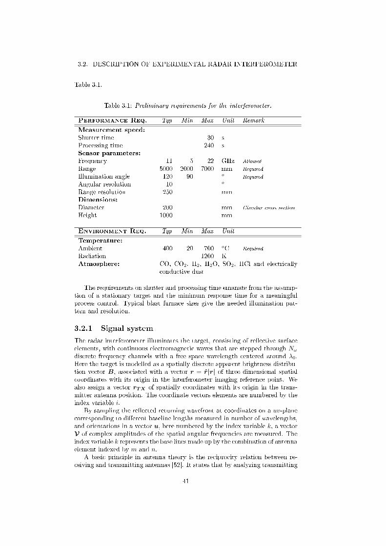
3.2. DESCRIPTION OF EXPERIMENTAL RADAR INTERFEROMETER
Table 3.1.
Table 3.1: Preliminary requirements for the interferometer.
Performance Req. Typ Min Max Unit Remark
Measurement speed:
Shutter time 30 sProcessing time 240 sSensor parameters:
Frequency 11 5 22 GHz Allowed
Range 5000 2000 7000 mm Required
Illumination angle 120 90 oRequired
Angular resolution 10 o
Range resolution 250 mmDimensions:
Diameter 200 mm Circular cross section
Height 1000 mm
Environment Req. Typ Min Max Unit
Temperature:
Ambient 400 -20 700 oC Required
Radiation 1200 KAtmosphere: CO, CO2, H2, H2O, SO2, HCl and electrically
conductive dust
The requirements on shutter and processing time emanate from the assump-tion of a stationary target and the minimum response time for a meaningfulprocess control. Typical blast furnace sizes give the needed illumination pat-tern and resolution.
3.2.1 Signal system
The radar interferometer illuminates the target, consisting of reective surfaceelements, with continuous electromagnetic waves that are stepped through Nωdiscrete frequency channels with a free space wavelength centered around λ0.Here the target is modelled as a spatially discrete apparent brightness distribu-tion vector B, associated with a vector r = r|r| of three dimensional spatialcoordinates with its origin in the interferometer imaging reference point. Wealso assign a vector rTX of spatially coordinates with its origin in the trans-mitter antenna position. The coordinate vectors elements are numbered by theindex variable i.
By sampling the reected returning wavefront at coordinates on a uv-planecorresponding to dierent baseline lengths measured in number of wavelengths,and orientations in a vector u, here numbered by the index variable k, a vectorV of complex amplitudes of the spatial angular frequencies are measured. Theindex variable k represents the base lines made up by the combination of antennaelement indexed by m and n.
A basic principle in antenna theory is the reciprocity relation between re-ceiving and transmitting antennas [52]. It states that by analyzing transmitting
41
CHAPTER 3. A MICROWAVE BASED IMAGING SENSOR
antennas we get the properties of receiving antennas as well. If we consider theantenna to be in the origin of a spherical coordinate system, r = (r, θ, φ), and ifr is suciently large, then the radiated electric- and magnetic-eld componentsare perpendicular to the vector r. This is the same as the far-eld or Fraun-hofer approximation being valid. The antenna pattern can now be stated asan r independent function F (θ, φ), commonly normalized to a maximum valueof one. The far-eld approximation starts to hold at a radial distance greaterthan,
Rff D2
λ0, (3.17)
where D is the diameter of the antenna. The half-power beamwidth is denedas the angular width of the main lobe between the two angles at which themagnitude of the antenna pattern, F (θ, φ), is equal to half of its peak value.
The directivity D(θ, φ) of an antenna in a direction is the ratio of its normal-ized radiation pattern F (θ, φ) in that direction, to its average over the completesphere. The maximum directivity D0 of an antenna is related to an eectivearea Ae of the antenna,
D0 =4π
λ20
Ae =4π
λ20
ηaAp, (3.18)
ηa is the aperture eciency and Ap is the physical aperture of the antenna.
The eciency factor ηa in (3.18) may also include ohmic losses and matchinglosses. The matching losses result in signal energy being reected back to thesource. The energy is, if reected back into the transmitter, lost in the sourceimpedance. If the received energy is reected back into the antenna, it will beretransmitted. In both cases it contributes to a lower signal level and a highernoise level. The mismatch energy may screen real targets or may be interpretedas a false target in a radar.
The eective aperture area Ae is important in the denition of the Friistransmission formula that relates transmitted power, Pt, to received power , Pr,in a transmission system. With a distance R between transmitter and receiverwe get
Pr =Pt
4πR2GtAe = SAe, (3.19)
where the available power density, S, is intercepted by the eective collectingantenna area.
The resolution of the interferometer is determined by microwave frequencybandwidth, microwave center frequency and the size of the interferometer aper-ture. The resolving power in radial direction is determined by microwave fre-quency bandwidth as in (3.2),
∆r = 0.443c0fBW
. (3.20)
The angular resolutions are determined by the uniformly weighted interferom-eter with the size D as,
∆θnadir ' 0.886λ0
D, (3.21)
42

3.2. DESCRIPTION OF EXPERIMENTAL RADAR INTERFEROMETER
and individual antenna element distribution function respectively. For otherlooking angles than nadir, we have to compute the angular resolution with aprojected aperture diameter as,
∆θ ' 0.886λ0
D cos(θ). (3.22)
In a cartesian coordinate system the radial and angular resolutions will becomecombined and quite dicult to dene. Around a position ri = (ri, θi, φi) theresolution in cartesian coordinates may be approximated with,
∆x ' ∆r sin θi + ri∆θ cos θi (3.23)
∆y ' ∆x (3.24)
∆z ' ∆r cos θi + ri∆θ sin θi. (3.25)
The sensitivity of the interferometer is determined by the noise, gain andintermodulation budget of each antenna element receiver chain. Since the inter-ferometer system transmits a CW signal at a low level of power, intermodulationis considered a non critical part of the system budget. A key parameter in anyradio system for radar or communication purposes is the signal to noise ratiodened as,
SNR =PrPn
, (3.26)
where Pn is the noise from the receiving system. The receiver noise is determinedby the system parameters, noise bandwidth, fLF, and system temperature, TSYS
or noise factor, FSYS. We have,
Pn = kTSYSfLF = kT0FSYSfLF, (3.27)
where k is the Boltzmann constant. With a denition of SNR that includesradar cross section, σ as,
SNR =PtG
2λ20σ
(4π)3R4Pn(3.28)
a minimum detectable Radar Cross Section (RCS) for a given minimum accept-able SNR can be calculated.
Phase errors and generation of the transmitted signal
Phase errors can be divided into two parts, random phase error (phase noise)and deterministic phase errors [43].
The phase noise of the signal limits the ability to focus the image. A stableand well controlled transmitter frequency is generated by use of phase lockedloops (PLL). The maximum possible rate of the frequency sweep is set by thephase noise requirements which in turn limits the shutter speed of the system.A fast frequency sweep requires a fast lock-in time as the output frequency isswept in steps. With a wide loop bandwidth we get a rapid response at the costof an increase in phase noise.
Minimum frequency step size is determined by the reference signal frequencyand the phase noise requirements of the PLL. Phase noise performance inside the
43

CHAPTER 3. A MICROWAVE BASED IMAGING SENSOR
loop bandwidth is governed by the reference signal. A small step size requires alow reference frequency, but the multiplication factor N needed to achieve theoutput frequency then is increased. Consequently also the output phase noisepower, which is the reference phase noise power increased with 20 logN in dB,is increased.
Dierent regions of oset frequencies for the phase noise, foffset, can beidentied. They are determined by the measurement range of the radar, orradar interferometer, and by the rate of the frequency sweep.
• Very short term phase drift, within duration of one frequency sample(foffset > 1000 Hz), reduce the receiver sensitivity.
• Short term phase drift, within one frequency sweep (5 Hz < foffset <1000 Hz), reduce the ability to compress the synthetic range pulse.
• Long term phase drift within one scan of the antenna ((1/30) Hz <foffset < 5 Hz), reduce the ability to compile the interferometric imagein cases of sequential baseline scans.
• Very long term phase drift limits the lifetime for the calibration measure-ments (foffset < (1/30) Hz).
Deterministic phase errors also eect the PSF of the system. These phaseerrors can be characterized by the group delay, or dispersion of the system.A signal phase shift that varies linearly with frequency gives a at group de-lay. Narrow-band resonant structures as sharp lters show a nonlinear phaseresponse, often sensitive to temperature variations. The use of bad calibrationdata is another source of deterministic phase errors. A simple classication ofdeterministic phase errors and their impact are listed below.
• Linear phase errors cause a spatial shift of the focused image.
• Quadratic errors cause a symmetric widening of the PSF, decreasing re-solution.
• Cubic errors cause unsymmetrical distortion of the PSF, decreasing reso-lution.
3.2.2 Interferometer array design
The actual sensor consists of an array of small antenna elements. Since wesample a nite aperture at a limited number of points, sidelobes occur, resultingin a so called dirty beam. Reduction of sidelobe energy can be performed bya weighting value wk for each baseline, but this reduces the eective aperturesize and thus the angular resolution. The dirty image with weighting functionbecomes,
di(τr) =∑k
wkVk(τr) exp(−j2πuk · ri), (3.29)
where uk are the coordinates on the uv-plane corresponding to the baselinesbeing sampled, Vk are the visibility functions from cross correlation of antennavoltages, ri is unit position vector, and τr is the delay time corresponding to
44

3.2. DESCRIPTION OF EXPERIMENTAL RADAR INTERFEROMETER
Figure 3.4: Baselines of the interferometer plotted on the uv-plane (in wavelength units). This plot shows the so called UV coverage of the interferometer.The lack of short baselines is a consequence of antenna isolation requirementsprohibiting antenna elements to be placed close to each other.
dierent radial distance from the interferometer. This gives a data set of radiallystacked two dimensional images in a non-Euclidian angular coordinate system,further described in [51]. Transformation to other coordinate systems can beperformed by a resampling procedure.
A second order error causing abberation will be introduced since we assumeplanar wavefronts and a small antenna, i.e. Fraunhofer diraction. The far-elddistance Rff where the Fraunhofer approximation starts to hold is given by,
Rff D2
λ0' max
k|uk|2λ0, (3.30)
where we used that (D ' maxk |uk|λ0). For our interferometer the far-eldapproximation is valid for distances greater than 849 mm. In the blast furnacethe interferometer is situated three to four meters above the burden surface.The usable eld of view for the interferometer is set by the individual antennaelement opening angle. Requirements from the application set this parameterto at least 90 degrees. The maximum measurable eld of view with the interfer-ometer is determined by the requirement that geometrical time delay in Fig.3.1,τg, should be less than f−1
LF . This, however, is of no concern in our case sincethe maximum baseline length covers only a few wavelengths and the steppedfrequency method gives us an instantaneous bandwidth, fLF, of a few tenths ofkHz. Further, the coherence time of the used signal source is far greater thanτg.
The angular resolution, or half-power beam width, in radians, of a two ele-ment interferometer is determined by the wavelength of the radiation and the
45

CHAPTER 3. A MICROWAVE BASED IMAGING SENSOR
length of the baseline Dλ, see Fig. 3.1, spanned by the antenna elements [53],
θ =1
2|Dλ|. (3.31)
Compared to the uniformly illuminated circular aperture this is an improvedresolution by a factor of 2. In the current application a resolution of about 10degrees has been considered to be sucient, see Tab. 3.1. With λ0 ' 27 mmand a interferometer diameter of 150 mm, we are well within the required reso-lution. The eective interferometer solid beam width Ωb is set by the baselinecoverage in two dimensions, and the illumination, or weighting, function used.Note that all surface elements dAi within the solid beam width Ωb are summedto produce the received brightness in each angular pixel. The number of suchsurface elements scale as r2
i , the brightness from each xed surface element scalesas r−2
i . The brightness received by the interferometer system per beam solidangle therefore is independent of the distance. The illumination of each surfaceelement is dependent on the distance to the transmitter r−2
TX. The brightnessper resolution pixel received by the radar interferometer signal is therefore pro-portional to r−2
TX. Radial full width at half power, ∆r, of the synthesized pulseis according to (3.2),
∆r = 0.443c0fBW
. (3.32)
In our case the bandwidth is fBW = 600 MHz giving a ∆r ' 220 mm. Thenumber of baselines in an interferometer is [46],
M =N(N − 1)
2, (3.33)
where N is the number of physical antenna elements. It would be preferred ifeach baseline gave a unique sample of the uv-plane since redundant baselinesadd no new structural information about the target, assuming a completelyincoherent surface brightness. Redundant samples merely increase the signal tonoise ratio. Although some methods [54] are proposed for minimum redundancyin distribution of the antennas, it is also known that, if N is large enough, it issucient to spread them out in a random fashion, as in this work. The coverageof the uv-plane of the interferometer is shown in Fig. 3.4
Making the antenna elements small compared to the free space wavelengthmakes it possible to both map a wide eld of view and tting a large numberof antennas inside the perimeter of the interferometer. A drawback of smallerantenna elements is the reduced antenna collecting area, resulting in a lowerSNR value. The choice of a planar antenna array gives a mechanical stableand accurate positioning of each element and an unsensitive surface. Antennaterminals are preferably placed on opposite side of the array than the patches,making the substrate surface less crowded and minimizing spurious radiation.A quadratic patch with circular polarization was designed. The use of circularpolarization makes it possible to rotate each antenna element in the plane of thearray, allowing an easier t and positioning of the elements. The constant phaseerror introduced by this rotation is compensated by a unitary complex coecientin the Fourier transform. A cross-section of the circuit substrate topology isshown in Fig. 3.6. When a combination of small size antenna element and low
46

3.2. DESCRIPTION OF EXPERIMENTAL RADAR INTERFEROMETER
Figure 3.5: Photo of the front of the patch antenna array showing antennaelements (patches).
Figure 3.6: Subsection of part of the antenna array showing substrates andmetallic layers making up circuits and antenna elements (patches).
47

CHAPTER 3. A MICROWAVE BASED IMAGING SENSOR
radiating resistance is wanted, conicting requirements on dielectric constantof the antenna substrate are raised. A compromise between size of patchesand radiation impedance was met by a using Duroid 3003, a substrate with adielectric constant of εr = 3.0. A low dielectric constant also reduce surfacewaves causing cross coupling between antenna elements [55]. Fig. 3.5 show thefront of the nal antenna array.
An aperture coupled, or slot coupled, patch antenna was considered to fullboth the requirements of easy planar fabrication and sucient bandwidth. Thismethod of coupling gives lower back radiation and the freedom to have dier-ent substrate thickness for circuitry and patches. A thicker antenna substrategives a more ecient radiating patch, while a thinner substrate for the circuitryreduce the back radiation [56]. Further, the patch covers the coupling aperture,reducing parasitic radiation from the ground plane slot. The slots are excitedby transmission lines feeded by a hybrid circuit.
The complete interferometer was integrated with a computer controlledswitch matrix and semirigid coaxial cables tted with coaxial push on con-nectors. The push on connectors makes it mechanically possible to mount avery dense microwave harness. Unwanted radiation from microstrip transmis-sion lines is minimized with this conguration, since all microstrip lines are veryshort and covered by the ground plane.
3.3 Results and discussion
The results presented here are from simulations with single and multiple discretetargets and from measurements. The interferometer functionality was veriedby measurements on single antenna elements and on a complete interferometersetup. A microwave vector network analyzer was used for the measurementsin both cases. A coaxial switch matrix was used to scan through the availableinterferometry data, assuming a steady state target surface. Simulated measure-ment data from an interferometer was generated by a ray tracing algorithm, andprocessed by a domain transforming algorithm. The same domain transform-ing algorithm, transferring data from spatial frequency domain to spatial delaydomain, was used for the measured data. A third algorithm was used for pre-sentation of the images. Yet other algorithms were made for testing CLEAN.
The patch antenna array was covered by a ceramic window and mounted ina dedicated protecting steel tube cooled with a continuous ow of nitrogen.
The simplest output data, except for cold sky noise measurement, is theresponse from a single scattering point target, see Fig. 3.7. Simulation of asingle target was used to obtain the point spread function(PSF) of the systemat dierent ranges and positions. Later these simulation could be used to verifythe actual measured PSF of the patch antenna array. The PSF is determinedby the bandwidth, (3.2), and the antenna array conguration.
The imaging possibility was tested by moving an active point source aroundon the laboratory oor. This veried the coordinate system and also that wewere able to nd the position of a reector in all three space coordinates. Theactive point source consisted of a wide opening angle antenna connected to thetransmitter output of the interferometer through a exible coaxial cable. Theactive point source was later replaced with a passive metallic reector madeout of copper, see Fig. 3.8. With this setup the crosstalk in the array was
48
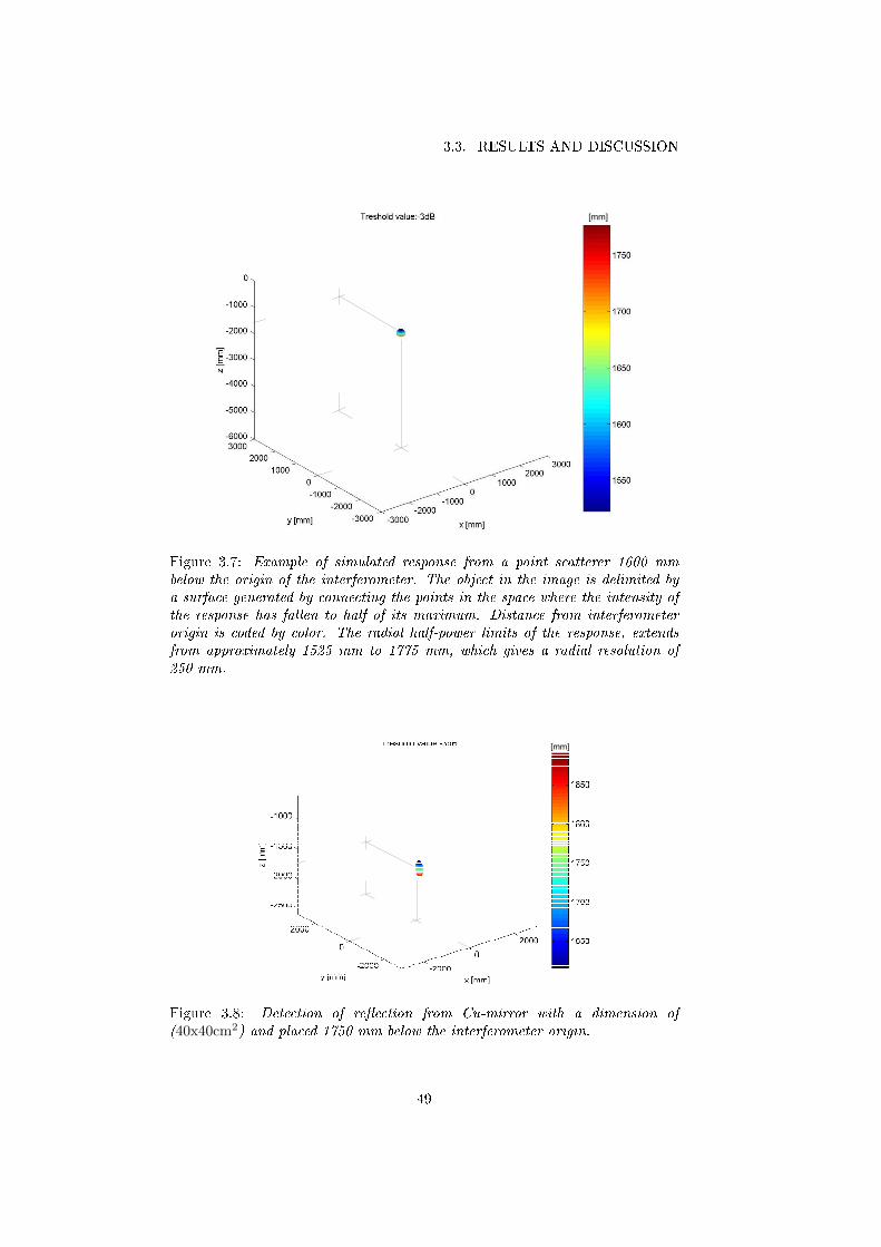
3.3. RESULTS AND DISCUSSION
[mm]
Figure 3.7: Example of simulated response from a point scatterer 1600 mmbelow the origin of the interferometer. The object in the image is delimited bya surface generated by connecting the points in the space where the intensity ofthe response has fallen to half of its maximum. Distance from interferometerorigin is coded by color. The radial half-power limits of the response, extendsfrom approximately 1525 mm to 1775 mm, which gives a radial resolution of250 mm.
Figure 3.8: Detection of reection from Cu-mirror with a dimension of(40x40cm2) and placed 1750 mm below the interferometer origin.
49

CHAPTER 3. A MICROWAVE BASED IMAGING SENSOR
Figure 3.9: The laboratory imaging experiment setup, in this case with cokespread on the oor. The interferometer array is found at the top center of theimage.
detected and could be spatially ltered by rejecting the response from the rstfew decimeters of the interferometer.
A layer of coke formed a surface on the oor of the laboratory. The surfacewas manually altered and measurements were taken between each alteration,see Fig. 3.9. Dierential images made by subtracting the datasets displayed asensitivity to these surface changes, Fig. 3.10. The measured result may be com-pared with the simulation in Fig. 3.11. Imperfections in the beam can be seentogether with sidelobes in the measurements. The sensitivity was improved bymoving the transmitter antenna, from within the array to an external position,thus reducing crosstalk.
The actual reconstruction of the surface is quite dicult and was underesti-mated in this project. By introducing several point targets in simulations, thespeckle phenomenon was studied and an approximation of a surface could bemade. A ray-tracing maximum intensity algorithm proved to be insucient.Speckle and sidelobes causing false detections make this approach impossibleeven in an ideal case. The maximum intensity algorithm detects the responsefrom the closest scatterer, which will dominate over more distant scatterers,
50

3.3. RESULTS AND DISCUSSION
Figure 3.10: Example of measured reection at radial distance 1786 mm comingfrom alterations made on the coke surface in Fig 3.9. Intensity is here normal-ized and coded by color. The unit of the axes is mm.
Figure 3.11: Simulated reection from changes in a reecting surface 1600 mmbelow and 1000 mm oset from the phase-center of the interferometer. Intensityis normalized and coded by color. The unit of axes is mm.
51

CHAPTER 3. A MICROWAVE BASED IMAGING SENSOR
and instead of the correct plane surface a bowled topography will be the out-put. Further, in an implemented interferometer the crosstalk between antennaelements will screen the real surface reections and cause false response. Aninitial attempt to use the CLEAN algorithm gave a promising response buthad a too long processing time, and the most distant and faint objects couldnot be properly detected, see Fig. 3.12. The CLEAN algorithm gave less falsedetections than the maximum intensity algorithm. A faster algorithm can beobtained, but it will still rest on the approximation of a limited number ofdiscrete point scatterers.
During the project we assumed a connected surface, but still there are dif-culties with hidden and shadowed regions that must be solved. Further, darkzones may be created by several mechanisms, such as specular reections di-rected away from the sensor, by lossy material, by depolarization or by speckle,or by sidelobes from close scatterers interfering destructively and cause darkzones.Using historical data of the surface topography is a good way to disqual-ify improbable solutions, such as sudden steps in height or tilting angle of thesurface. Thus, the nal surface model must include a multitude of parameters,such as speckle, specular reection, surface roughness and scales, shadowing,sidelobes, depolarization, spatial history and history in time.
The experiments show that the radar interferometer is sensitive to surfacealterations, and that it may be assembled from relatively low cost components.For its utilization in industrial process control the signal processing has to befurther developed and the protective encapsulation has to be improved. Radioastronomy signal processing methods have often shown to be inappropriate forradar interferometry due to the spatial coherency of the source.
52

3.3. RESULTS AND DISCUSSION
Figure 3.12: CLEAN algorithm output from simulation of 16 scatterers evenlydistributed on a slanting plane, in xy- and xz-plane. The correct position of thescatterers are indicated by the crossings of the help grid lines. Note that thez-axis is reversed compared to other images. Unit of axes is mm.
53

CHAPTER 3. A MICROWAVE BASED IMAGING SENSOR
54

Chapter 4
Conclusion and outlook
4.1 Conclusion
Low power solutions have become increasingly important for electronic design[7], and low power radio can be achieved when power is prioritized already inthe system design phase. On-chip integration of radio electronics is part of thesolution, but it also bring new diculties to address.
The most interesting technology platform for low cost radio nodes is theCMOS process. CMOS process development is mainly driven by the require-ments of digital electronics, and radio designers have to adopt accordingly. Theupside of the ongoing reduction of linewidths is the increase of available transi-tion frequency ft of transistors, which is benecial for the RF designer. However,along with the reduced transistor size comes an increased sensitivity to over-voltage, where the gate oxide is the most sensitive part. It takes only a fewvolts over the gate oxide to damage the insulation. Addition of on-chip ESDprotection circuitry to counteract over-voltage comes at a cost of added par-asitic loads. These parasitic elements have to be be taken into account whendesigning the RF front end.
In some cases the ESD protection circuitry will be the limiting factor of per-formance, leading to a complicated trade-o between performance and level ofprotection. Further there is a reluctance to add any external components whenadding new functionality to an ASIC. This goes also for wake-up functional-ity, which ideally should be implemented as an IP-block to any general ASIC.This basically restricts the technologies available for implementation of WuRsto ordinary CMOS processes.
The ever increasing use of electronic equipment in general, and radio equip-ment specically, increase the levels of EM-interference. The situation is com-plex without a good overall picture of the existing interference environment.For many systems the sensitivity analysis is dominated by interference ratherthan the thermal noise. This problem must be addressed by both MAC protocolinnovations and by hardware innovations (regulative work must also take thenew situation into account). New tools for analysis are needed for ecient tradeos in the system design phase.
Ecient MAC protocols are needed for better spectrum eciency [29][26].The synchronization in the protocols depend on accurate timing and/or accurate
55

CHAPTER 4. CONCLUSION AND OUTLOOK
frequency control [57][58]. Inaccuracy in frequency will force MAC designers toinsert larger guard bands reducing the spectrum eciency. Drift in time resultsin longer awake time for duty cycled receivers causing increased energy con-sumption. Accuracy in time and frequency require well performing resonatorsor delay lines. A good resonator should be stable and independent of environ-ment variables as temperature and vibration. While low loss resonators tend tobe bulky and expensive, stability can be reached by arrangements like ovens orcompensating and controlling electronics, at the cost of power and componentcount. Lossy resonators need to be compensated with active ampliers to formoscillators, but still they exhibit phase noise due to their losses. This impliesthat precision in time and frequency is unachievable in applications requiringboth low power and small sized radio nodes.
Key components are resonant tanks and reactive loads needed for oscillators,lters, transformers, and ampliers. Well performing reactive components aredicult to minimize and/or to integrate. Integrated on-chip inductors oer lowQ-value and occupy large and costly silicon area. Therefore on-chip inductorsare costly and not very attractive in solutions for tank circuits. Using lowergrade resonators mean higher loss and therefore a need to compensate withhigher gain which in turn leads to increased power consumption. Further, theeect of losses can not be totaly overcome by active components, noise, phasenoise and jitter will still be the result. With higher carrier frequencies the useof distributed components on substrate can oer a reduced component cost, butthis requires stable and good quality substrates; for moderate frequencies FR4has proven to perform quite well. High quality substrate materials with lowloss are expensive and have relatively low dielectric constants, this leads to tankcircuits occupying fairly large areas.
At lower frequencies active inductors is an alternative although they areinherently more noisy than their passive counterparts. Finally, an interestingand a bit surprising result from this work is that resistive loads are competitivewith passive and active inductors as output load for integrated ampliers evenat radio frequencies.
Microwaves have the ability to both sense and carry information over dis-tance. The integration of microwave and digital electronics enable sensor appli-cations requiring heavy computational resources at low power and low cost, suchas imaging interferometers or similar antenna arrays. This heavy integration isnow possible even at mm-Wave frequencies [59], but the volumes are often tosmall to justify the cost [60].
4.2 Outlook
Wireless Sensor Networks (WSN) is a kind of synthesis of sensors and RFID.In a larger perspective these sensor networks are the elements that become theInternet of Things (IoT), which is visioned to create wisdom out of data as inFig. 4.1.
IoT has been sketched as a three layered architecture, see Fig. 4.2, withpowerful computing and data storage facilities in the innermost core, and witha swarm of sensors all around us in the outmost layer of the architecture [61].In between, hand held devices will mediate the information and present thestored and processed data from the core. This communication between layers
56

4.2. OUTLOOK
Figure 4.1: A vision of how data is transformed to wisdom by the Internet ofThings (IoT). Data is collected from sensors and transferred and processed byubiquitous low power electronics.
Figure 4.2: A vision of how IoT is made up of dierent structural layers [61].Radio will be used for communication between layers, while remote sensing willbe used in the outmost layer.
57

CHAPTER 4. CONCLUSION AND OUTLOOK
needs to be wireless, with a high degree of exibility and a good coverage, andis predicted to essentially be one of the most challenging details of the systemto realize [7]. Microwaves will be used for communication and sensing at alllevels. However, there are wide variation in the requirements. While the com-munication between the innermost core and the middle layer may require datarates of 100 Mbps and very low latencies (<1ms) everywhere, the communica-tion between the sensors and the middle layer may be measured in kbits persecond and with an undetermined latency period. In the latter case the mostimportant building block from a power perspective in the wireless communica-tion chain is the receiver of the sensor rather than the transmitter. This is aresult of long inactivity periods, where transmitters are asleep but the receivershave to always be awake.
IoT, Ubiquitous Computing, and Pervasive Computing are all terms witha similar meaning, describing a widespread occurrence of radio nodes in oureveryday life. The nodes may perform simple tasks and between uptime havelong periods of inactivity. They must be small, cheap, and functional for severalyears without need for service. Improved logistics, tracking of goods, trans-portation management, and sensing are some of the motivational factors behindthe development. This has pushed the RFID technology forward, and the needfor large numbers of nodes requires extremely low cost solutions.
As the IoT is expected to be a part of our everyday life and incorporatedin critical systems such as medical devices and transport systems its robustnessis vital. The constituting nodes has to withstand environmental factors suchas temperature, moist, shock, vibrations, and a very dynamic and changingelectromagnetic situation.
The described requirements of small size, low power consumption, robust-ness, and low unit cost, are very demanding. These issues can only be solvedif one considers the total system, with its radio nodes, readers, back end sys-tems, software, hardware, and protocols as a whole. Thus a close collaborationbetween designers at dierent layers and a focus on application is necessary.Application focused design may however result in very heterogenous solutionsbeing dicult to merge with other systems.
The size of each node is many times set by the battery and the antenna. Newantenna designs are needed that better make use of the total volume availablefor the node instead of being two-dimensions structures only. Prediction of theantenna coupling to the environment is dicult for mobile devices and furtherrequires comprehensive simulations throughout the design phase. Batteries mustnot only be dimensioned to supply the average power needed, but also the peakpowers developing during start up and at transmission bursts.
Energy scavenging technology is improving making it possible to counteractthe battery drain or to remove batteries completely. Energy scavenging makeuse of vibrations, light, thermal energy, and electromagnetic smog. Ability tostore energy in super capacitors and batteries make such solutions more robust.These otherwise unreliable and unstable energy sources call for ways to evaluatequality and stability and possibly to dynamically modulate the load [62]. Sup-plying energy over the air with the RF-signal is today commonly used in RFIDtechnology and oer good system control over the energy source. Research ishere made to improve RF-DC conversion and to lower radio power consump-tion on the chip, but eorts are also made by investigating power optimizedwaveforms having higher peak to average power ratios [63].
58

4.2. OUTLOOK
New materials and processes result in new components for high speed elec-tronics. Examples are graphene transistors and wrapped gate transistors [64].MEMS technology oer new low loss resonators; Bulk Acoustic Wave (BAW) l-ters are used for pre-selective lter at radio frequencies [15]. Battery technologyis improving with higher energy densities, being exploited to make radio nodessmaller and live longer. Flexible solutions with printed batteries oer modestenergy density and low peak power, but also the possibility to tailor the batterysize and form factor. Mechanically exible battery materials must be developedto ensure new and ductile form factors. A designer further wants exibility inher choice of battery capacity so she can optimize the lifetime of the radio node.
Moores law still holds and we may expect digital electronics to push linewidths to be smaller, enabling high speed transistors possible to use in sub-threshold regime for radio electronics. The cost per radio node is reduced as sil-icon footprint is reduced, and more functionality may be integrated. This is trueas long as many identical units can be fabricated. For low volume productionthere are possibilities to use FPGA, and a growing availability of programmableradio ASICs o the shelf. Miniaturization may be an issue with such solutions,but as discussed earlier, batteries and antennas are the largest components. Theincreased computation capabilities with digital electronics can be used for builtin self test (BIST) methods and in-vivo calibration. This may e.g. be used todynamically compensate antenna mismatch due to changing electromagnetic en-vironment of the radio [9] or to overcome spread in material parameters. BISTfurther provides tuning possibility of poor frequency and time reference oscilla-tors. MAC protocols may include processes for periodical tuning of the nodesto a common reader reference [31]. Massive MIMO is yet another microwaveapplication made possible with improved computational capacity.
Old analog wireless services are closed and frequency bands are freed up thatmay host smarter digital applications. The use of higher carrier frequencies isexploited for higher data rates, to escape to quieter frequency bands and lim-iting the interfering range (60 GHz). Higher carrier frequencies further enableminiaturization of antennas and for beam forming with reasonable sized arrays.Higher frequencies take on more sophisticated production methods, often ex-pensive, and the use of new unproven materials or production methods to meetperformance.
Radio communication has for a long time focused on providing larger band-width with higher data rates. This has lead to the use of increased carrier fre-quencies, higher density of radio cells and shorter communication ranges (e.g.60 GHz WLAN). However, today in many radio applications (e.g. military,leisure, and sport) there must be an increased awareness of the radio environ-ment and of the user behavior. Such new intelligent radio systems form ad hocnetworks, and instead provide the bandwidth or range needed for the situation.
Modern radio systems are in many cases limited by interference rather thanby thermal noise. New methods and components have to be developed to helpsystem designers in their work. An example is multiband radio frontends thatcould be realized with generic wideband Software Dened Radio (SDR). Such areceiver solution could replace several separate hardware receiver blocks, mini-mize cost and maintain exibility. However, the receiver is consequently exposedto a wide spectrum of interfering signals. The required dynamic range of thereceiver to be handled is set by the level of interference. The required dynamicrange of the receiver, and thereby the power consumption, could eectively be
59

CHAPTER 4. CONCLUSION AND OUTLOOK
reduced by ltering out out-of-band interfering signals in a preselecting lter.However, today there is no good solution for such an interference managingpreselecting lter with low power consumption, high dynamic range, small size,being electronically controllable over a wide bandwidth.
From being rare and sometimes referred to as black magic, microwave tech-nology has become omnipresent in, and essential for, the vision of ubiquitouscomputing and IoT. Further, considering the development of power consump-tion, there is obviously plenty of room at the bottom.
60

References
[1] E. Nilsson and L. Baath, Multi-dimensional imaging method and appara-tus, U.S. Patent US 2007/0 109 177 A1, 17, 2007.
[2] The internet of things how the next evolution of the internet is changingeverything, White Paper, Cisco, 2011.
[3] J. Rabaey, M. Ammer, J. da Silva, J.L., D. Patel, and S. Roundy, Picoradiosupports ad hoc ultra-low power wireless networking, Computer, vol. 33,no. 7, pp. 4248, Jul 2000.
[4] J. Paradiso and T. Starner, Energy scavenging for mobile and wirelesselectronics, Pervasive Computing, IEEE, vol. 4, no. 1, pp. 1827, Jan.-March 2005.
[5] H. Yan, J. G. Macias-Montero, A. Akhnoukh, L. C. N. de Vreede, J. R.Long, and J. N. Burghartz, An ultra-low-power BPSK receiver and demod-ulator based on injection-locked oscillators, IEEE Trans. Microw. TheoryTech., vol. 59, pp. 13391348, May 2011.
[6] E. H. Armstrong, Some recent developments of regenerative circuits, Pro-ceedings of the IRE, vol. 10, Aug. 1922.
[7] B. Otis and J. Rabaey, Ultra-Low Power Wireless Technologies for SensorNetworks. New York: Springer, 2007.
[8] H. L. Thal, New radiation Q limits for spherical wire antennas, IEEETrans. Antennas Propag., vol. 54, pp. 27572763, Oct. 2006.
[9] C. W. P. F et al., A 2.4GHz CMOS automatic matching network design forpacemaker applications, in Circuits and Systems and TAISA Conference,2009, Jun. 2009, pp. 14.
[10] P. Sjoblom and H. Sjoland, An adaptive impedance tuning CMOS circuitfor ISM 2.4-GHz band, Circuits and Systems I: Regular Papers, IEEETransactions on, vol. 52, no. 6, pp. 11151124, 2005.
[11] D. C. Daly, P. P. Mercier, M. Bhardwaj, A. L. Stone, Z. N. Aldworth, T. L.Daniel, J. Voldman, J. G. Hildebrand, and A. P. Chandrakasan, A pulsedUWB receiver SoC for insect motion control, IEEE J. Solid-State Circuits,vol. 45, pp. 153166, Jan. 2010.
61
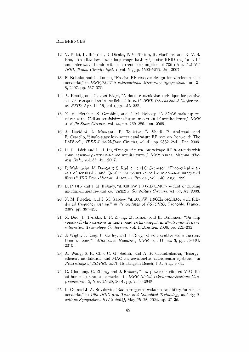
REFERENCES
[12] V. Pillai, H. Heinrich, D. Dieska, P. V. Nikitin, R. Martinez, and K. V. S.Rao, An ultra-low-power long range battery/passive RFID tag for UHFand microwave bands with a current consumption of 700 nA at 1.5 V,IEEE Trans. Circuits Syst. I, vol. 54, pp. 15001512, Jul. 2007.
[13] P. Kolinko and L. Larson, Passive RF receiver design for wireless sensornetworks, in IEEE/MTT-S International Microwave Symposium, Jun. 38, 2007, pp. 567570.
[14] A. Hennig and G. vom Bögel, A data transmission technique for passivesensor-transponders in medicine, in 2010 IEEE International Conferenceon RFID, Apr. 1416, 2010, pp. 215222.
[15] N. M. Pletcher, S. Gambini, and J. M. Rabaey, A 52µW wake-up re-ceiver with -72dBm sensitivity using an uncertain-IF architechture, IEEEJ. Solid-State Circuits, vol. 44, pp. 269280, Jan. 2009.
[16] A. Liscidini, A. Mazzanti, R. Tonietto, L. Vandi, P. Andreani, andR. Castello, Single-stage low-power quadrature RF receiver front-end: TheLMV cell, IEEE J. Solid-State Circuits, vol. 41, pp. 28322841, Dec. 2006.
[17] H.-H. Hsieh and L.-H. Lu, Design of ultra-low-voltage RF frontends withcomplementary current-reused architectures, IEEE Trans. Microw. The-ory Tech., vol. 55, Jul. 2007.
[18] R. Malmqvist, M. Danestig, S. Rudner, and C. Svensson, Theoretical anal-ysis of sensitivity and Q-value for recursive active microwave integratedlters, IEE Proc.-Microw. Antennas Propag., vol. 146, Aug. 1999.
[19] B. P. Otis and J. M. Rabaey, A 300-µW 1.9-GHz CMOS oscillator utilizingmicromachined resonators, IEEE J. Solid-State Circuits, vol. 38, Jul. 2003.
[20] N. M. Pletcher and J. M. Rabaey, A 100µW, 1.9GHz oscillator with fullydigital frequency tuning, in Proceedings of ESSCIRC, Grenoble, France,2005, pp. 387390.
[21] X. Duo, T. Torikka, L.-R. Zheng, M. Ismail, and H. Tenhunen, On-chipversus o-chip passives in multi-band radio design, in Electronics System-integration Technology Conference, vol. 1, Dresden, 2006, pp. 221232.
[22] J. Wight, J. Long, L. Carley, and T. Riley, On-die synthesized inductors:Boon or bane? Microwave Magazine, IEEE, vol. 11, no. 3, pp. 95104,2010.
[23] A. Wang, S.-H. Cho, C. G. Sodini, and A. P. Chandrakasan, Energy-ecient modulation and MAC for asymmetric microsensor systems, inProceedings of ISLPED 2001, Huntington Beach, CA, Aug. 2001.
[24] G. Chunlong, C. Zhong, and J. Rabaey, Low power distributed MAC forad hoc sensor radio networks, in IEEE Global Telecommunications Con-ference, vol. 5, Nov. 2529, 2001, pp. 29442948.
[25] L. Gu and J. A. Stankovic, Radio-triggered wake-up capability for sensornetworks, in 10th IEEE Real-Time and Embedded Technology and Appli-cations Symposium, RTAS 2004), May 2528, 2004, pp. 2736.
62

REFERENCES
[26] S. Drago, F. Sebastiano, L. Breems, D. Leenaerts, K. Makinwa, andB. Nauta, Impulse-based scheme for crystal-less ULP radios, Circuits andSystems I: Regular Papers, IEEE Transactions on, vol. 56, no. 5, pp. 10411052, May 2009.
[27] R. Floyd, RFID: Yesterday, today, and tomorrow, Potentials, IEEE,vol. 31, no. 6, pp. 1146, 2012.
[28] J. Landt, The history of RFID, Potentials, IEEE, vol. 24, no. 4, pp. 811,2005.
[29] B. Nilsson, L. Bengtsson, B. Svensson, U. Bilstrup, and P.-A. Wiberg, Anactive backscatter wake-up and tag identication extraction protocol forlow cost and low power active RFID, in RFID-Technology and Applications(RFID-TA), 2010 IEEE International Conference on, Jun. 2010, pp. 86 91.
[30] J.-Y. Chen, M. P. Flynn, and J. P. Hayes, A fully integrated auto-calibrated super-regenerative receiver in 0.13-µm CMOS, IEEE J. Solid-State Circuits, vol. 42, Sep. 2007.
[31] J. Ayers, K. Mayaram, and T. Fiez, An ultralow-power receiver for wirelesssensor networks, Solid-State Circuits, IEEE Journal of, vol. 45, no. 9, pp.1759 1769, Sep. 2010.
[32] E. Nilsson and C. Svensson, Envelope detector sensitivity and blockingcharacteristics, in Circuit Theory and Design (ECCTD), 2011 20th Euro-pean Conference on, Aug. 2011, pp. 773 776.
[33] IEEE Std 802.3-2008 (Revision of IEEE Std 802.3-2005).
[34] X. Huang, S. Rampu, X. Wang, G. Dolmans, and H. de Groot, A2.4GHz/915MHz 51µW wake-up receiver with oset and noise suppres-sion, in IEEE International Solid-State Circuits Conference 2010, Feb. 9,2010, pp. 222224.
[35] Auto-ID Center. (2002) 860MHz-930MHz class I radio frequencyidentication tag radio frequency and logical communication interfacespecication candidate recommendation, version 1.0.1. [Online]. Available:www.gs1.org/epcglobal/standards/specs
[36] S. Solda, M. Caruso, A. Bevilacqua, A. Gerosa, D. Vogrig, and A. Neviani,A 5 Mb/s UWB-IR transceiver front-end for wireless sensor networks in0.13 µm CMOS, Solid-State Circuits, IEEE Journal of, vol. 46, no. 7, pp.1636 1647, Jul. 2011.
[37] A. Gerosa, S. Solda, A. Bevilacqua, D. Vogrig, and A. Neviani, An energy-detector for noncoherent impulse-radio UWB receivers, Circuits and Sys-tems I: Regular Papers, IEEE Transactions on, vol. 56, no. 5, pp. 10301040, May 2009.
[38] T. Orhaug and B. Höglund, Rymdkommunikationsteknik, 5th ed., Göte-borg, 1974.
63
REFERENCES
[39] C. Svensson and J. J. Wikner, Power consumption of analog circuits: atutorial, Analog Integrated Circuits and Signal Processing, vol. 65, Nov.2010.
[40] J.-Y. Park, D.-W. Kim, Y.-S. Son, J.-C. Ha, J.-K. Song, C.-S. Jang, andW.-Y. Jung, Low-capacitance low-voltage triggered SCR ESD clamp usingnMOS with asymmetric drain for RF ICs, Microwave Theory and Tech-niques, IEEE Transactions on, vol. 59, no. 2, pp. 360367, 2011.
[41] C. A. Balanis, Antenna Theory. hoboken: Wiley, 2005.
[42] B. Razavi, A study of phase noise in CMOS oscillators, Solid-State Cir-cuits, IEEE Journal of, vol. 31, no. 3, pp. 331343, 1996.
[43] W. G. Carrara, R. S. Goodman, and R. M. Majewski, Spotlight SyntheticAperture Radar: Signal Processing Algorithms. Norwood: Artech house,1995.
[44] P. Dammert, Accuracy of INSAR measurements in forested areas,in FRINGE 96, Zurich, Switzerland, Oct. 1996. [Online]. Available:http://www.geo.unizh.ch/rsl/fringe96/papers/dammert/
[45] C. T. Wang, H. T. Wang, D. C. Chern, N. Y. Chen, and L. S.Liang, A study on dierential interferometry in subsidence, inProceedings ACRS, Taipei, Taiwan, Dec. 2000. [Online]. Available:http://www.gisdevelopment.net/aars/acrs/2000/ts14/sari0004.asp
[46] A. R. Thompson, J. M. Moran, and J. George W. Swenson, Interferometryand Synthesis in Radio Astronomy, 2nd ed. USA: John Wiley and Sons,2001.
[47] J. Starck, E. Pantin, and F. Murtagh, Deconvolution in astronomy: Areview, Astronomical Society of the Pacic, pp. 10511069, Oct. 2002.
[48] T. Cornwell and K. Evans, A simple maximum entropy deconvolutionalgorithm, Astronomy and Astrophysics, pp. 7783, 1985.
[49] J. Hogbom, Aperture synthesis with a non-regular distribution of inter-ferometer baselines, Astronomy and Astrophysics Supplement, vol. 15, pp.417426, Jun. 1974.
[50] R. Bose, A. Freedman, and B. Steinberg, Sequence CLEAN: a modieddeconvolution technique for microwave images of contiguous targets, IEEETrans. Aerosp. Electron. Syst., vol. 38, pp. 8997, Jan. 2002.
[51] E. Nilsson and L. B. Baath, Radar interferometric measurements with aplanar patch antenna array, IEEE Sensors J., 2006.
[52] P.-S. Kildahl, Foundation of Antennas. Lund, Sweden: Studentlitteratur,2000.
[53] F. T. Ulaby, R. K. Moore, and A. K. Fung, Microwave Remote Sensing,Active and Passive. Norwood, MA: Artech House, 2003.
64
REFERENCES
[54] A. T. Moet, Minimum-redundancy linear arrays, IEEE Trans. AntennasPropag., vol. 16, pp. 172175, Mar. 1968.
[55] D. M. Pozar, Microwave Engineering. Amherst, MA: John Wiley andSons, 1998.
[56] R. Garg, P. Bhartia, I. Bahl, and A. Ittipiboon, Microstrip Antenna DesignHandbook. Norwood, USA: Artech House, 2001.
[57] F. Sebastiano, L. Breems, K. Makinwa, S. Drago, D. Leenaerts, andB. Nauta, A low-voltage mobility-based frequency reference for crystal-less ULP radios, Solid-State Circuits, IEEE Journal of, vol. 44, no. 7, pp.2002 2009, july 2009.
[58] U. Denier, Analysis and design of an ultralow-power CMOS relaxationoscillator, Circuits and Systems I: Regular Papers, IEEE Transactionson, vol. 57, no. 8, pp. 1973 1982, Aug. 2010.
[59] J. Laskar, CMOS, cognitive and mmW: A wireless revolution, in Radioand Wireless Symposium (RWS), 2012 IEEE, 2012, pp. 211214.
[60] M. Tiebout, H. D. Wohlmuth, H. Knapp, R. Salerno, M. Druml, M. Rest,J. Kaeferboeck, J. Wuertele, S. Ahmed, A. Schiessl, R. Juenemann, andA. Zielska, Low power wideband receiver and transmitter chipset for mm-wave imaging in SiGe bipolar technology, Solid-State Circuits, IEEE Jour-nal of, vol. 47, no. 5, pp. 11751184, 2012.
[61] J. Rabaey, The swarm at the edge of the cloud - a new perspective onwireless, in VLSI Circuits (VLSIC), 2011 Symposium on, 2011, pp. 68.
[62] T. Burd, T. Pering, A. Stratakos, and R. Brodersen, A dynamic volt-age scaled microprocessor system, Solid-State Circuits, IEEE Journal of,vol. 35, no. 11, pp. 15711580, 2000.
[63] M. Trotter and G. Durgin, Survey of range improvement of commercialRFID tags with power optimized waveforms, in RFID, 2010 IEEE Inter-national Conference on, Apr. 2010, pp. 195 202.
[64] E. Lind and L.-E. Wernersson, Design of RF properties for verticalnanowire MOSFETs, Nanotechnology, IEEE Transactions on, vol. 10,no. 4, pp. 668673, 2011.
65


![FM Microwave Radio Link - Elber radio TV broadcast …UserManuals~NBFM_[EN].pdfFM Microwave Radio Link Transmitter T_NBFM-01 ... microwave radio link. It is able to transfer, over](https://static.fdocuments.net/doc/165x107/5ab9bcd47f8b9aa6018e34cf/fm-microwave-radio-link-elber-radio-tv-broadcast-usermanualsnbfmenpdffm.jpg)

