APPLIED PHYSICS Copyright © 2021 Meta-optics achieves RGB ...
9
Li et al., Sci. Adv. 2021; 7 : eabe4458 27 January 2021 SCIENCE ADVANCES | RESEARCH ARTICLE 1 of 8 APPLIED PHYSICS Meta-optics achieves RGB-achromatic focusing for virtual reality Zhaoyi Li 1 *, Peng Lin 2 , Yao-Wei Huang 1,3 , Joon-Suh Park 1,4 , Wei Ting Chen 1 , Zhujun Shi 1,5 , Cheng-Wei Qiu 3 , Ji-Xin Cheng 2,6 , Federico Capasso 1 * Virtual and augmented realities are rapidly developing technologies, but their large-scale penetration will require lightweight optical components with small aberrations. We demonstrate millimeter-scale diameter, high-NA, submicron-thin, metasurface-based lenses that achieve diffraction-limited achromatic focusing of the primary colors by exploiting constructive interference of light from multiple zones and dispersion engineering. To illus- trate the potential of this approach, we demonstrate a virtual reality system based on a home-built fiber scanning near-eye display. INTRODUCTION Optical lenses are in demand more than ever before. They are being widely used in electronic devices such as smart phones. Unlike elec- tronics that has rapidly evolved and shrunk in size following the Moore’s law over the past decades, the appearance and the underly- ing physics of today’s optical lenses are similar to the Nimrud lens dating back to ~3000 years ago (1, 2). Light focusing by a refractive lens relies on accumulation of propagation phase, and thus, lens thickness scales up as diameter (3). Moreover, multilens sets, such as doublets and triplets, are required to correct chromatic aberra- tions. Fresnel lenses have a reshaped compact form yet suffer from poor imaging quality due to their strong chromatic aberrations (2) and other limitations. Achromatic lenses, such as camera objectives, have a large form factor due to their composite nature, which imposes a bottleneck to next-generation optical systems such as wearable display in terms of footprint, imaging quality, complexity, and cost. Metasurfaces have emerged as a platform for novel flat optics in recent years (4, 5). They are arrays of nanostructures assembled on a subwavelength scale, which can mold electromagnetic wavefronts at will. Metalenses, in particular, have been widely studied to ad- dress the challenges of conventional optics and show considerable potential for practical applications (6–8). Fundamentally different from traditional lenses, metalenses are optically thin and light and can be designed to correct monochromatic and chromatic aberrations without requiring the complexity of refractive optics by controlling the phase, amplitude, and polarization state of the transmitted light with subwavelength resolution; high numerical aperture (NA) is easy to achieve in metalenses (9). In recent works, researchers have demonstrated metalenses working in the visible based on new ma- terial platforms (10, 11) and by complementary metal-oxide semi- conductor (CMOS)–compatible fabrication techniques (12) that are feasible for mass production of large-diameter metalenses. Researchers have realized achromatic metalenses over broad band- width by locally engineering waveguide modes (or resonate modes) of meta-atoms to compensate chromatic dispersion (13–18). How- ever, such achromatic metalenses have a diameter size of tens of micron due to limited group delay achievable with meta-atoms (19), limiting their practical use. Here, we present a general design prin- ciple to achieve large-area, multiwavelength achromatic metalenses. We demonstrate in the experiment the 2-mm-diameter red-green- blue (RGB)–achromatic transmissive metalenses. Furthermore, we demonstrate a compact virtual reality (VR) platform based on the RGB-achromatic metalens and a fiber scanning near-eye display. RESULTS Design principles Traditional optical lenses suffer from chromatic aberrations limit- ing their imaging performance. The chromatic aberration of a re- fractive lens originates from the intrinsic material dispersion that causes longer wavelengths to focus at longer focal distance. In com- parison, the focusing of a diffractive lens, Fresnel lens for example, is more than 10 times dispersive. Such severe chromaticity is mainly due to phase discontinuities at zone boundaries. It results in longer focal distances for shorter wavelengths (2). The form factor and the chromatic aberration of a traditional optical lens are hard to reduce at the same time. To address such a challenge, we introduce a mul- tizone dispersion-engineered metalens (Fig. 1A) by using a design principle as described in Eq.1 ~ E ( ) = i=1 N ( ∫ ri−1 ri t(, r ) e i∅ i(,r) rdr ) e i∆∅ i() = i=1 N ~ E i ( ) e i∆∅ i() (1) where N is the number of zones, and r i is the radial coordinate of each zone boundary (r 0 = 0); t(, r) characterizes the amplitude of the scattered electric field by meta-atoms at a frequency of ; ∅ i (, r) is the designed phase profile within the ith zone; and ∆∅ i () is the phase discontinuity at the boundary between (i − 1)th and ith zone [∆∅ 1 () = 0]. The electric field ~ E () at the focal spot is determined by the interference of electric field within each zone [t(, r)e i∅ i (, r) ] and the interference of the electric fields [ ~ E i ()] from N different zones (Fig. 1A). To maximize the focusing intensity ∣ ~ E ( 0 )∣ 2 at a single frequency 0 , the desired phase profile within each zone should be hyperbolic, i.e., ∅ i ( 0 , r ) = 0 ⁄ c(F( 0 ) − √ _ F ( 0 ) 2 + r 2 ), where F( 0 ) is the focal length at frequency 0 ; in addition, the phase discontinuities at the zone boundaries should be zero, ∆∅ i ( 0 ) = 0. 1 Harvard John A. Paulson School of Engineering and Applied Sciences, Harvard Univer- sity, Cambridge, MA 02138, USA. 2 Department of Electrical and Computer Engineer- ing, Boston University, Boston, MA 02215, USA. 3 Department of Electrical and Computer Engineering, National University of Singapore, Singapore, Singapore. 4 Nanopho- tonics Research Center, Korea Institute of Science and Technology, Seoul, Republic of Korea. 5 Department of Physics, Harvard University, Cambridge, MA 02138, USA. 6 Department of Biomedical Engineering, Boston University, Boston, MA 02215, USA. *Corresponding author. Email: [email protected] (Z.L.); capasso@seas. harvard.edu (F.C.) Copyright © 2021 The Authors, some rights reserved; exclusive licensee American Association for the Advancement of Science. No claim to original U.S. Government Works. Distributed under a Creative Commons Attribution NonCommercial License 4.0 (CC BY-NC). on January 27, 2021 http://advances.sciencemag.org/ Downloaded from
Transcript of APPLIED PHYSICS Copyright © 2021 Meta-optics achieves RGB ...

Li et al., Sci. Adv. 2021; 7 : eabe4458 27 January 2021
S C I E N C E A D V A N C E S | R E S E A R C H A R T I C L E
1 of 8
A P P L I E D P H Y S I C S
Meta-optics achieves RGB-achromatic focusing for virtual realityZhaoyi Li1*, Peng Lin2, Yao-Wei Huang1,3, Joon-Suh Park1,4, Wei Ting Chen1, Zhujun Shi1,5, Cheng-Wei Qiu3, Ji-Xin Cheng2,6, Federico Capasso1*
Virtual and augmented realities are rapidly developing technologies, but their large-scale penetration will require lightweight optical components with small aberrations. We demonstrate millimeter-scale diameter, high-NA, submicron-thin, metasurface-based lenses that achieve diffraction-limited achromatic focusing of the primary colors by exploiting constructive interference of light from multiple zones and dispersion engineering. To illus-trate the potential of this approach, we demonstrate a virtual reality system based on a home-built fiber scanning near-eye display.
INTRODUCTIONOptical lenses are in demand more than ever before. They are being widely used in electronic devices such as smart phones. Unlike elec-tronics that has rapidly evolved and shrunk in size following the Moore’s law over the past decades, the appearance and the underly-ing physics of today’s optical lenses are similar to the Nimrud lens dating back to ~3000 years ago (1, 2). Light focusing by a refractive lens relies on accumulation of propagation phase, and thus, lens thickness scales up as diameter (3). Moreover, multilens sets, such as doublets and triplets, are required to correct chromatic aberra-tions. Fresnel lenses have a reshaped compact form yet suffer from poor imaging quality due to their strong chromatic aberrations (2) and other limitations. Achromatic lenses, such as camera objectives, have a large form factor due to their composite nature, which imposes a bottleneck to next-generation optical systems such as wearable display in terms of footprint, imaging quality, complexity, and cost.
Metasurfaces have emerged as a platform for novel flat optics in recent years (4, 5). They are arrays of nanostructures assembled on a subwavelength scale, which can mold electromagnetic wavefronts at will. Metalenses, in particular, have been widely studied to ad-dress the challenges of conventional optics and show considerable potential for practical applications (6–8). Fundamentally different from traditional lenses, metalenses are optically thin and light and can be designed to correct monochromatic and chromatic aberrations without requiring the complexity of refractive optics by controlling the phase, amplitude, and polarization state of the transmitted light with subwavelength resolution; high numerical aperture (NA) is easy to achieve in metalenses (9). In recent works, researchers have demonstrated metalenses working in the visible based on new ma-terial platforms (10, 11) and by complementary metal-oxide semi-conductor (CMOS)–compatible fabrication techniques (12) that are feasible for mass production of large-diameter metalenses.
Researchers have realized achromatic metalenses over broad band-width by locally engineering waveguide modes (or resonate modes)
of meta-atoms to compensate chromatic dispersion (13–18). How-ever, such achromatic metalenses have a diameter size of tens of micron due to limited group delay achievable with meta-atoms (19), limiting their practical use. Here, we present a general design prin-ciple to achieve large-area, multiwavelength achromatic metalenses. We demonstrate in the experiment the 2-mm-diameter red-green-blue (RGB)–achromatic transmissive metalenses. Furthermore, we demonstrate a compact virtual reality (VR) platform based on the RGB-achromatic metalens and a fiber scanning near-eye display.
RESULTSDesign principlesTraditional optical lenses suffer from chromatic aberrations limit-ing their imaging performance. The chromatic aberration of a re-fractive lens originates from the intrinsic material dispersion that causes longer wavelengths to focus at longer focal distance. In com-parison, the focusing of a diffractive lens, Fresnel lens for example, is more than 10 times dispersive. Such severe chromaticity is mainly due to phase discontinuities at zone boundaries. It results in longer focal distances for shorter wavelengths (2). The form factor and the chromatic aberration of a traditional optical lens are hard to reduce at the same time. To address such a challenge, we introduce a mul-tizone dispersion-engineered metalens (Fig. 1A) by using a design principle as described in Eq.1
~ E ( ) = i=1 N ( ∫ r i−1 r i t(, r ) e i ∅ i (,r) rdr ) e i∆ ∅ i () = i=1 N ~ E i ( ) e i∆ ∅ i ()
(1)
where N is the number of zones, and ri is the radial coordinate of each zone boundary (r0 = 0); t(, r) characterizes the amplitude of the scattered electric field by meta-atoms at a frequency of ; ∅i(, r) is the designed phase profile within the ith zone; and ∆∅i() is the phase discontinuity at the boundary between (i − 1)th and ith zone [∆∅1() = 0]. The electric field ~ E () at the focal spot is determined by the interference of electric field within each zone [t(, r)ei∅i(, r)] and the interference of the electric fields [ ~ E i () ] from N different zones (Fig. 1A). To maximize the focusing intensity ∣ ~ E ( 0 )∣ 2 at a single frequency 0, the desired phase profile within each zone should be hyperbolic, i.e., ∅ i ( 0 , r ) = 0 ⁄ c (F( 0 ) − √
_ F ( 0 ) 2 + r 2 ) ,
where F(0) is the focal length at frequency 0; in addition, the phase discontinuities at the zone boundaries should be zero, ∆∅i(0) = 0.
1Harvard John A. Paulson School of Engineering and Applied Sciences, Harvard Univer-sity, Cambridge, MA 02138, USA. 2Department of Electrical and Computer Engineer-ing, Boston University, Boston, MA 02215, USA. 3Department of Electrical and Computer Engineering, National University of Singapore, Singapore, Singapore. 4Nanopho-tonics Research Center, Korea Institute of Science and Technology, Seoul, Republic of Korea. 5Department of Physics, Harvard University, Cambridge, MA 02138, USA. 6Department of Biomedical Engineering, Boston University, Boston, MA 02215, USA.*Corresponding author. Email: [email protected] (Z.L.); [email protected] (F.C.)
Copyright © 2021 The Authors, some rights reserved; exclusive licensee American Association for the Advancement of Science. No claim to original U.S. Government Works. Distributed under a Creative Commons Attribution NonCommercial License 4.0 (CC BY-NC).
on January 27, 2021http://advances.sciencem
ag.org/D
ownloaded from

Li et al., Sci. Adv. 2021; 7 : eabe4458 27 January 2021
S C I E N C E A D V A N C E S | R E S E A R C H A R T I C L E
2 of 8
To achieve controlled focusing at different frequencies, we set an multiobjective optimization function as max(min( ∣ ~ E ( i ) ∣ 2 ) ) , where i ∈ {1, 2⋯n} is the design frequency. It means to maximize the minimum value of the focusing intensity at design frequencies. In our design, we engineered the lens phase profiles (Fig. 1B) within each zone according to Eq. 2
∅ i (ω, r ) = ω ─ c ( F(ω ) − √ _
F (ω) 2 + r 2 ) + ∅ 0 (ω)
= ω 0 ─ c ( F( ω 0 ) − √ _
F ( ω 0 ) 2 + r 2 ) + ∂ ∅ i (ω, r) ─ ∂ ω (ω − ω 0 ) +
∂ 2 ∅ i (ω, r) ─ 2 ∂ ω 2
(ω − ω 0 ) 2 + ∅ 0 (ω)
(2)
where F() is the focal length at frequency , r is the radial coordi-nate, 0 is the center design wavelength, and ∅0() is the phase at the metalens center. This designed phase profile was realized by us-ing spatially varied meta-atoms that can independently control phase and dispersion (group delay ∂ ∅ i ⁄ ∂ , group delay dispersion ∂ 2 ∅ i ⁄ ∂ 2 ). In this way, light from an individual zone constructively interfere at a focal spot for all design frequencies. Furthermore, we engineer zone interference using an inverse design method. To be more spe-cific, we optimize the zone transition locations ri and the phase dis-continuities ∆∅i() using the method of moving asymptotes, which is a gradient-based local optimization method (20). The engineered meta-atoms also allow imposing an additional ∆∅i() onto each zone’s phase profile ∅i(, r) without altering local phase gradient
D
E
F
G
A
B C
Fig. 1. Design and simulations of an RGB-achromatic metalens. (A) Schematic drawing of a multizone RGB-achromatic metalens showing achromatic focusing of RGB light coming from different lens locations. ~ E () represents the interferenced complex electric field at the focal spot of frequency . (B) One example of the phase profile, the group delay (GD) profile, and the group delay dispersion (GDD) profile designed for a multizone, RGB-achromatic metalens. The zone is defined by an area with con-tinuously changed dispersion. Phase discontinuities at zone boundaries, zone transition locations, and initial phase at the lens centers require independent control. (C) Schematic drawing of a Fresnel lens phasor diagram and a metalens phasor diagram at a design focal spot. Phase discontinuities of a metalens can be independently engineered without changing the dispersion within each zone. (D) Simulated focusing intensity distribution of the metalens with NA = 0.7 along its optical axis at design wavelengths of 488, 532, and 658 nm. The inset is the zoomed-in view of focusing peaks. a.u., arbitrary units. (E to G) Simulation results of the intensity profiles in the focal planes at the design wavelengths.
on January 27, 2021http://advances.sciencem
ag.org/D
ownloaded from
Li et al., Sci. Adv. 2021; 7 : eabe4458 27 January 2021
S C I E N C E A D V A N C E S | R E S E A R C H A R T I C L E
3 of 8
and, thus, light interference within each zone, as can be seen that ∆∅i() is independent on lens location r within each zone, i.e., ∂ ∆ ∅ i () ⁄ ∂ r = 0 . The phase discontinuity at a certain frequency is related to the center frequency 0 in a following way
∆ ∅ (ω, r i ) = ∆ ∅ ( ω 0 , r i ) + ω 0 ─ c (F( ω 0 ) − √
_ F ( ω 0 ) 2 + r i
2 ) −
ω ─ c (F(ω ) − √ _
F (ω) 2 + r i 2 )
(3)
The details of design principles are explained in the Supplemen-tary Materials (section S1). The ability to independently engineer phase profile, dispersion within each zone, and phase discontinu-ities at zone boundaries rewrites the physics governing a Fresnel lens, in which these parameters cannot be independently controlled. Figure 1C shows phasor diagrams of a typical Fresnel lens and our dispersion-engineered metalens at the design focal spot highlight-ing their differences. The result of zone interference can be under-stood as lining up phasor units [ ~ E i () ] contributed by each zone with certain angles that are determined by phase discontinuities at zone boundaries [∆∅i()]. In the Fresnel lens, phase discontinuities at design frequency (2) are kept zero for constructive interference. However, destructive interference occurs at other frequencies (e.g., 1 and 3) caused by their fixed nonzero phase discontinuities and intrinsic material dispersion. In comparison, in our metalens, pha-sor units [ ~ E i () ] within each zone and phase discontinuities [∆∅i()] at each zone boundary are both engineered to realize the overall constructive interference at the design wavelengths.
Simulation results of large RGB-achromatic metalensesBy applying the above principles, we designed two 2-mm-diameter metalenses with NAs of 0.7 and 0.3, with the goal of focusing three primary RGB colors at the same focal length [F() = F0] while sup-pressing spurious focal spots elsewhere along the optical axes. Using the first three zones of an RGB-achromatic metalens for illustration, Fig. 1B shows examples of the designed phase profile, the group de-lay (GD) profile, and the group delay dispersion (GDD) profile from top to bottom, respectively. Here, GDmin and GDmax are the mini-mum and maximum group delays, which are bounded by the meta- atom library. Figure 1B also highlights other key design parameters including phase discontinuity ∆∅i, initial phase ∅0, and zone loca-tion ri, which are inversely designed. We can increase the size of the metalens by increasing the zone number N, and we show simulation results of a 1-cm-diameter RGB-achromatic metalens (section S2). We can also apply this design principle to engineer light focusing at more than three colors by increasing the number of design frequen-cies in optimization.
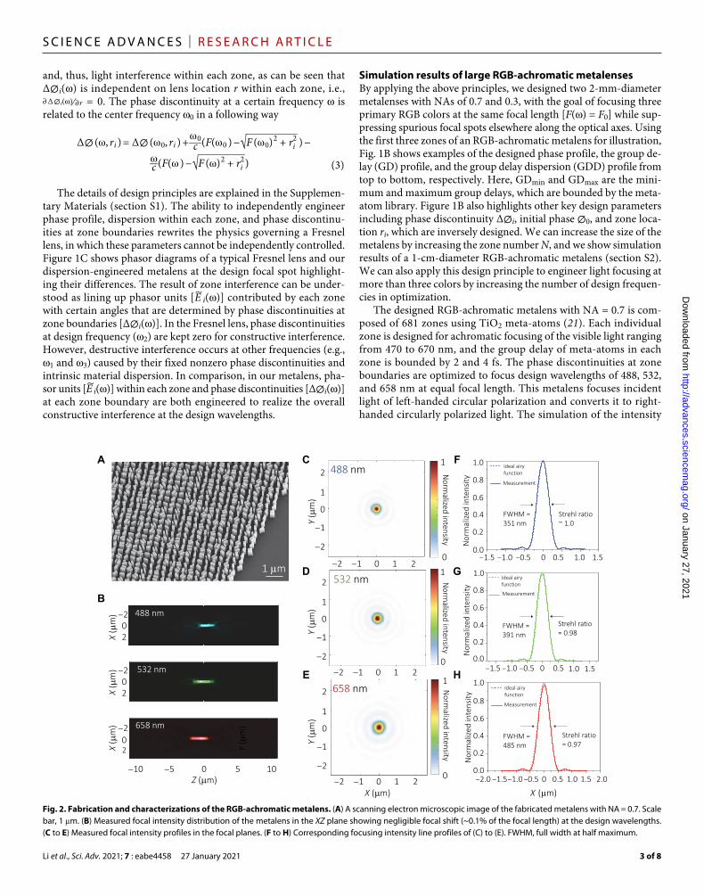
The designed RGB-achromatic metalens with NA = 0.7 is com-posed of 681 zones using TiO2 meta-atoms (21). Each individual zone is designed for achromatic focusing of the visible light ranging from 470 to 670 nm, and the group delay of meta-atoms in each zone is bounded by 2 and 4 fs. The phase discontinuities at zone boundaries are optimized to focus design wavelengths of 488, 532, and 658 nm at equal focal length. This metalens focuses incident light of left-handed circular polarization and converts it to right- handed circularly polarized light. The simulation of the intensity
A
B
C
D
E
F
G
H
Fig. 2. Fabrication and characterizations of the RGB-achromatic metalens. (A) A scanning electron microscopic image of the fabricated metalens with NA = 0.7. Scale bar, 1 m. (B) Measured focal intensity distribution of the metalens in the XZ plane showing negligible focal shift (~0.1% of the focal length) at the design wavelengths. (C to E) Measured focal intensity profiles in the focal planes. (F to H) Corresponding focusing intensity line profiles of (C) to (E). FWHM, full width at half maximum.
on January 27, 2021http://advances.sciencem
ag.org/D
ownloaded from

Li et al., Sci. Adv. 2021; 7 : eabe4458 27 January 2021
S C I E N C E A D V A N C E S | R E S E A R C H A R T I C L E
4 of 8
distribution at three wavelengths along the optical axis by using the Fresnel-Kirchhoff integral method (22) shows pronounced focusing peaks at the design focal length with negligible intensity elsewhere (Fig. 1D). The inset is the zoom-in view showing the same focal length at the design wavelengths. Figure 1 (E to G), shows the sim-ulated intensity profiles of focal spots at three design wavelengths in the plane perpendicular to the optical axis (Z axis). The calculated Strehl ratios are all close to unity, indicating diffraction-limited fo-cusing. For the metalens with NA = 0.3, we optimized not only the phase discontinuities at zone boundaries but also the zone transi-tion locations and the RGB wavelengths. The optimization goals are maximizing the light intensity at the design focal spots and mini-mizing spurious focusing elsewhere along the optic axis (multifoci). Simulation results are summarized in section S3. The calculated Strehl ratios are also close to unity, and the intensity of spurious focal spots is greatly suppressed.
Focusing and imaging characterizations of the RGB-achromatic metalensesFigure 2A shows a scanning electron microscope image of the fab-ricated 2-mm-diameter metalens with NA = 0.7 (see section S4 for additional images). The metalens is composed of TiO2 nanofins of different geometries and rotation angles that are tailored for inde-pendent control of phases and dispersion. Figure 2B shows the mea-sured focal intensity profile in the XZ plane of the metalens at the design wavelengths. The setup and measurement details are illus-trated in section S3. The maximum focal shift among three focal spots at the RGB wavelengths is around 1 m, which is ~0.1% of the
design focal length. The error arises from fabrication imperfections. Figure 2 (C to E) shows the measured intensity distribution in the focal plane, and the corresponding Strehl ratios at the design wave-lengths are all close to unity, as shown in Fig. 2 (F to H). Such near-ly ideal focusing is the result of the combined effects of dispersion engineering and zone interference engineering. The RGB focusing of the metalens with NA = 0.3 is similarly achromatic and diffrac-tion limited (section S3).
We characterized imaging of the metalens by using the USAF (United States Air Force) resolution target. For the metalens with NA = 0.7, we imaged elements no. 5 and no. 6 from group no. 7 using laser diodes with linewidths of ~1 nm (Fig. 3, A to C). The measurement setup is explained in detail in section S5. The smallest feature size is ~2.2 m. The metalens not only resolves each bar but also captures the subtle imperfections of the bar edges. The slight blur is due to coma aberration. We also tested the imaging of this metalens in other synthesized colors by mixing two incident light sources (Fig. 3, D to F). Figure 3 (G and H) shows the imaging re-sults under white light illumination synthesized by combining RGB laser diodes. We characterized the metalens with NA = 0.3 by imag-ing the whole group no. 7 of the resolution target. Here, we used a tunable supercontinuum laser (linewidth > 5 nm) as a light source, and results are shown in Fig. 3 (I to K). Figure 3L shows the white light imaging result by combining RGB laser sources, and the imag-ing results of two-color mixing are summarized in section S5. The coma aberration of this metalens is less pronounced due to its smaller NA. We observed that imaging blur occurs when increas-ing light source linewidth (section S5).
A B C
I J K L
D
E F G H
Fig. 3. Imaging of the USAF resolution target by the RGB-achromatic metalenses under different illumination. (A to C) Imaging results of the elements no. 5 and no. 6 from the group no. 7 of a USAF resolution target by the metalens with NA = 0.7 at design wavelengths of = 488, 532, and 658 nm, respectively. The smallest line-width feature size is 2.2 m. Scale bars, 10 m. (D to F) Imaging results of the same target by the metalens of NA = 0.7 under synthesized light illumination by mixing two and (G and H) all three of the RGB laser sources. Scale bars, 10 m. (I to K) Imaging results of the whole group no. 7 of the USAF resolution target by the metalens with NA = 0.3 at design wavelengths of = 470, 548, and 647 nm, respectively. Scale bars, 30 m unless noted. (L) Imaging result of the target by the metalens under synthe-sized white light illumination that is composed of the RGB wavelengths.
on January 27, 2021http://advances.sciencem
ag.org/D
ownloaded from

Li et al., Sci. Adv. 2021; 7 : eabe4458 29 January 2021
S C I E N C E A D V A N C E S | R E S E A R C H A R T I C L E
5 of 8
Virtual and augmented reality demonstrationThe diffraction-limited and RGB-achromatic focusing performances of our metalens are desirable for applications in compact image projection systems (23, 24), which have light emission centered at three discrete RGB wavelengths. Recent advances in VR technolo-gies are hindered by eyepieces because of their bulky size (25, 26), heavy weight, and compromised viewing experience (27). Here, we demonstrated a VR platform on the basis of an RGB-achromatic metalens. The schematic of the VR system is shown in Fig. 4A (top).
An achromatic metalens is placed in front of an eyeball, and a display is placed within the focal plane of the metalens. The images shown on the display are magnified by the metalens, focused onto retina through eye lens crystal, and form virtual images appearing at far distance. In the experiment, we used a tube lens to mimic the eye lens crystal and a CMOS camera to mimic the retina. Figure 4A (bottom) is the cross-sectional view illustrating the VR system working principle. We show key design parameters of a VR device in section S6. The field of view (FOV) is determined by the NA of an
BA
C D
E F G H
I J K L
M N O P
Fig. 4. VR demonstration. (A) Top: Schematic illustration of the VR mode. Bottom: Cross-section view illustrating its working principle. FML is the focal length of the metalens, and L (~7 cm) is the eye relief distance. (B) Schematic illustration of the near-eye fiber scanning display. (C) The VR imaging result using a passive display under the green light illumination at = 548 nm. Scale bar, 20 m. (D) Zoomed-in view of (C). The dots inside the shield pattern, which mimic pixel grains, have a diameter of 1300 nm and can be clearly resolved (see fig. S21). Scale bar, 10 m. (E to H) Four binary optical images captured in the VR mode at = 548 nm. The images are displayed by scanning the fiber tip in a Lissajous pattern and temporally modulating the incident light’s intensity in two levels (on/off). Scale bars, 20 m unless noted. (I to K) Virtual objects with a three-dimensional (3D) effect, which are displayed by applying multilevel intensity modulation. (L to N) VR images of G, B, and R letters with a 3D effect in three distinct colors by using continuous-level intensity modulation of incident light. (O) An RGB-color VR imaging result. (P) A VR image showing a “H” logo shield in seven colors, which are realized by mixing the primary RGB colors in space and time.
on January 27, 2021http://advances.sciencem
ag.org/D
ownloaded from

Li et al., Sci. Adv. 2021; 7 : eabe4458 27 January 2021
S C I E N C E A D V A N C E S | R E S E A R C H A R T I C L E
6 of 8
eyepiece; the form factor is determined by the size of the eyepiece and the display as well as by the distance between them. A desirable VR system should consist of a high-NA eyepiece and a miniaturized display. So far, most VR devices on the market are based on bulky refractive lenses, which suffer from not only chromatic aberrations but also low-NA focusing. For example, we characterized a lens from a commercial VR device (section S7). Meta-optics provides an alternative approach due to their combined merits.
Another challenge in current VR technologies is a desired near-eye display that offers combined advantages such as miniaturized footprint, high resolution, high dynamic range, high brightness, and wide color gamut. To achieve that, we first used a passive display that is mimicked by using patterned metal masks and laser beam illumination (section S8). We further developed a fiber scanning method for a near-eye display (28). Figure 4B depicts the schematic of a fiber scanning display. An optical fiber was mounted through a piezo actuator tube with the fiber tip positioned at distance L from the piezo. An electric signal was applied to the piezo actuator tube by two pairs of electrodes that were soldered onto the end of the tube. The applied voltage controls the movement of the fiber in two orthogonal directions and thus the trajectory of the fiber tip. The fiber tip scans in two dimensions and displays patterns when the incident light is guided through the optical fiber, thus forming a miniaturized display. To display arbitrary design patterns, light emission was modulated as a function of time in synchronization with the fiber tip movement (section S8). Fundamentally different from traditional liquid crystal display (LCD)/light-emitting diode (LED) displays where the pixel number is predefined by the single pixel size and the display size and the pixels are uniformly distributed in two-dimensional (2D) lattices, here, the pixel number of the fiber scanning display is determined by its light modulation speed, and the pixel distribution depends on its scanning method. We used and compared two scanning methods: Lissajous scanning and spiral scan-ning. The voltage signals applied onto the two electrodes are in the following form: Vx(y)(t) = Ax(y)(t) sin (2fx(y)t + x(y)) where Ax(y) is the voltage amplitude in x(y) direction, fx(y) is the modulation fre-quency, and x(y)is the initial phase. The details of our applied fiber scanning techniques are discussed in section S8. Figure 4C shows the VR imaging result using a passive display under green light illumi-nation. Figure 4D is the zoomed-in view of Fig. 4C and shows clearly resolved dots inside the shield pattern that mimic pixels (section S8). The dots have a diameter of 1300 nm, which are smaller than the pixel sizes (~8 m) of current micro-LCD (micro-LED) display
on the market. Figure 4 (E to P) shows the VR imaging results using our home-built near-eye fiber scanning display. Figure 4 (E to H) shows four binary imaging examples consisting of 1 megapixel using green incident light in a VR demo. The fiber tip scans in a Lissajous pattern. The imaging results using red and blue incident light are shown in section S8. As can be seen from the virtual imag-es captured by the camera, the light intensity distribution is quite uniform and the image resolution is reasonably high. The imaging results using the spiral scanning method are shown in section S8. Next, we demonstrated grayscale imaging that creates a 3D effect by applying a multilevel voltage to the acoustic-optic modulator. Figure 4 (I and J) shows a Penrose triangle image with four-level intensity and a Penrose square image with five-level intensity, re-spectively. A toroid image with a continuous intensity variation is also shown in Fig. 4K, which demonstrates the high dynamic range of the fiber scanning display. Figure 4 [L to N (three images)] shows gray-scale images of RGB letters with 3D effects in distinct colors. We furthermore realized a full-color fiber scanning display by combin-ing three different laser sources (section S8). Figure 4O shows a three-primary- color image displaying RGB letters in grayscale that is captured in VR mode. Figure 4P shows an H-letter-embodied shield logo in seven colors, of which three are primary RGB colors defined by the laser sources and the other four realized by color mixing. The RGB laser source linewidths are smaller than 5 nm, which infers wide color gamut (section S9). The footprint of the fiber scanning display could be reduced toward a portable device, and possible strategies are discussed in section S10. We compared the perform ance of our fiber scanning near-eye display with cur-rent existing display techniques on the market, and the results are summarized in section S9.
In addition, the RGB-achromatic metalens can be implemented into an augmented reality (AR) device, as shown in Fig. 5A. It al-lows the mixture of virtual objects and real-world scenes through an optical combiner (section S12). Figure 5B is the AR imaging result using the passive display. It shows that a virtual purple H-letter- embodied shield immerses in a real-world scene. Figure 5 (C and D) is the AR imaging result using the near-eye fiber scanning display, which shows floating virtual images of gadget icons and three-color RGB letters in a real-world scene, respectively (more information in section S12). Current challenges in VR/AR open new opportunities for dispersion-engineered metasurfaces, as discussed in section S13. For example, we designed a compact achromatic quarter wave plate on the basis of dispersion-engineered metasurfaces in simulation
DCBA
Fig. 5. AR demonstration. (A) Schematic illustration of the AR mode. (B) An AR image showing a floating H-shield logo pattern in purple color created by using a passive display immerses in a real-world scene. (C) An AR image showing the mixture of a real-world scene with a floating image that is created by the near-eye fiber scanning display. (D) The AR imaging result using the full-color near-eye fiber scanning display, which shows an RGB-color virtual image floating in a real-world scene. Photo credit: Zhaoyi Li, Harvard University.
on January 27, 2021http://advances.sciencem
ag.org/D
ownloaded from

Li et al., Sci. Adv. 2021; 7 : eabe4458 27 January 2021
S C I E N C E A D V A N C E S | R E S E A R C H A R T I C L E
7 of 8
and proposed a strategy to resolve eye’s depth of cue by using a multi-focal RGB-achromatic metalens.
DISCUSSIONFurther improvements are desirable for better implementation of a metalens in image projection applications. First, one challenge of a high-NA metalens is limited FOV. The metalens shown in this work corrects monochromatic aberrations and chromatic aberration for normal incidence. Its higher-order aberrations limit the VR device’s FOV to be <10°. We showed in simulation an RGB metalens dou-blet that can also correct coma aberration, field curvature, and transverse chromatic aberration for oblique incident beams for large FOV (section S14) (29, 30). Second, one can further increase the size of the metalens to centimeter scale and use the fabrication tech-niques that are feasible for large scale and mass production at low cost, such as deep UV (ultraviolet) stepper lithography (12, 31, 32), nanoimprint lithography (33), surface plasmon lithography (34), etc. Third, the focusing efficiency of the metalens can be improved by using multilayer unit cells and topological optimized meta-atoms in the future.
The co-engineering of dispersion and zone interference opens a new paradigm of metalens design, which represents a combination of forward and inverse design methods. We have demonstrated a path to a large yet thin lens that can simultaneously achieve diffraction- limited high-NA achromatic focusing at multiple wavelengths by engineering meta-atoms’ dispersion and controlling constructive interference at every location. The meta-optics demonstrated in this work offer new paths to future VR/AR applications.
MATERIALS AND METHODSSimulationThe metalens is composed of TiO2 nanofin structures. The building block library was built up by using the rigorous coupled-wave anal-ysis method and consisted of ~60,000 nanostructures with different geometries. The height of the TiO2 nanofin is 600 nm and the peri-odicity of the unit cell is 400 nm. The incident light is set as a left-handed circularly polarized state, and the monitored trans-mitted light is in the conjugate right-handed circularly polariza-tion state.
FabricationThe metalens presented was fabricated on fused silica substrate in the following procedures: To begin with, the fused silica substrate was spun coated with a layer of 600-nm-thick positive electron beam resist (Zeon Chemicals, ZEP-520A), followed by an additional layer of conductive polymer (Showa Denko, ESPACER 300) to avoid charging effects during electron beam lithography. After that, the patterns were defined using electron beam lithography (Elionix, ELS-F125), and the exposed sample was then developed in o-xylene. Next, around 210-nm-thick amorphous TiO2 was deposited directly onto the developed sample using atomic layer deposition (Cambridge Nanotech, Savannah). The TiO2 not only filled in the trenches of the exposed e-beam resist but also coated on top of the unexposed sample area. We later removed the excess film of the TiO2 by using reactive ion etching (Oxford Instrument, PlasmaPro 100 Cobra 300), and the etchant is a mixture of CHF3, O2, and Ar gas. Upon the completion of the etching processing, we stripped off the electron
beam resist by soaking the sample in Remover PG (MicroChem Corporation) for 24 hours.
SUPPLEMENTARY MATERIALSSupplementary material for this article is available at http://advances.sciencemag.org/cgi/content/full/7/5/eabe4458/DC1
REFERENCES AND NOTES 1. A. H. Layard, Discoveries in the Ruins of Nineveh and Babylon: With Travels in Armenia,
Kurdistan and the Desert (John Murray, 1853). 2. D. C. O'Shea, T. J. Suleski, A. D. Kathman, D. W. Prather, Diffractive Optics: Design,
Fabrication, and Test (Spie Press Bellingham, WA, 2004), vol. 62. 3. R. Kingslake, R. B. Johnson, Lens Design Fundamentals (Academic Press, 2009). 4. N. Yu, F. Capasso, Flat optics with designer metasurfaces. Nat. Mater. 13, 139–150 (2014). 5. H.-T. Chen, A. J. Taylor, N. Yu, A review of metasurfaces: Physics and applications.
Rep. Prog. Phys. 79, 076401 (2016). 6. M. Khorasaninejad, F. Capasso, Metalenses: Versatile multifunctional photonic
components. Science 358, eaam8100 (2017). 7. D. Lin, P. Fan, E. Hasman, M. L. Brongersma, Dielectric gradient metasurface optical
elements. Science 345, 298–302 (2014). 8. M. L. Tseng, H. H. Hsiao, C. H. Chu, M. K. Chen, G. Sun, A. Q. Liu, D. P. Tsai, Metalenses:
Advances and applications. Adv. Opt. Mater. 6, 1800554 (2018). 9. R. Paniagua-Domínguez, Y. F. Yu, E. Khaidarov, S. Choi, V. Leong, R. M. Bakker, X. Liang,
Y. H. Fu, V. Valuckas, L. A. Krivitsky, A. I. Kuznetsov, A metalens with a near-unity numerical aperture. Nano Lett. 18, 2124–2132 (2018).
10. M. Khorasaninejad, W. T. Chen, R. C. Devlin, J. Oh, A. Y. Zhu, F. Capasso, Metalenses at visible wavelengths: Diffraction-limited focusing and subwavelength resolution imaging. Science 352, 1190–1194 (2016).
11. B. H. Chen, P. C. Wu, V. C. Su, Y. C. Lai, C. H. Chu, I. C. Lee, J. W. Chen, Y. H. Chen, Y. C. Lan, C. H. Kuan, D. P. Tsai, GaN metalens for pixel-level full-color routing at visible light. Nano Lett. 17, 6345–6352 (2017).
12. A. She, S. Zhang, S. Shian, D. R. Clarke, F. Capasso, Large area metalenses: Design, characterization, and mass manufacturing. Opt. Express 26, 1573–1585 (2018).
13. Z. Shi, M. Khorasaninejad, Y. W. Huang, C. Roques-Carmes, A. Y. Zhu, W. T. Chen, V. Sanjeev, Z. W. Ding, M. Tamagnone, K. Chaudhary, R. C. Devlin, C. W. Qiu, F. Capasso, Single-layer metasurface with controllable multiwavelength functions. Nano Lett. 18, 2420–2427 (2018).
14. S. Wang, P. C. Wu, V. C. Su, Y. C. Lai, M. K. Chen, H. Y. Kuo, B. H. Chen, Y. H. Chen, T. T. Huang, J. H. Wang, R. M. Lin, C. H. Kuan, T. Li, Z. Wang, S. Zhu, D. P. Tsai, A broadband achromatic metalens in the visible. Nat. Nanotechnol. 13, 227–232 (2018).
15. S. Shrestha, A. C. Overvig, M. Lu, A. Stein, N. Yu, Broadband achromatic dielectric metalenses. Light 7, 85 (2018).
16. F. Aieta, M. A. Kats, P. Genevet, F. Capasso, Multiwavelength achromatic metasurfaces by dispersive phase compensation. Science 347, 1342–1345 (2015).
17. S. Wang, P. C. Wu, V.-C. Su, Y.-C. Lai, C. H. Chu, J.-W. Chen, S.-H. Lu, J. Chen, B. Xu, C.-H. Kuan, T. Li, S. Zhu, D. P. Tsai, Broadband achromatic optical metasurface devices. Nat. Commun. 8, 187 (2017).
18. M. Pu, X. Li, X. Ma, Y. Wang, Z. Zhao, C. Wang, C. Hu, P. Gao, C. Huang, H. Ren, X. Li, F. Qin, J. Yang, M. Gu, M. Hong, X. Luo, Catenary optics for achromatic generation of perfect optical angular momentum. Sci. Adv. 1, e1500396 (2015).
19. W. T. Chen, A. Y. Zhu, F. Capasso, Flat optics with dispersion-engineered metasurfaces. Nat. Rev. Mater. 5, 604–620 (2020).
20. K. Svanberg, A class of globally convergent optimization methods based on conservative convex separable approximations. SIAM J. Optim. 12, 555–573 (2002).
21. R. C. Devlin, M. Khorasaninejad, W. T. Chen, J. Oh, F. Capasso, Broadband high-efficiency dielectric metasurfaces for the visible spectrum. Proc. Natl. Acad. Sci. 113, 10473–10478 (2016).
22. G. Kirchhoff, Zur theorie der lichtstrahlen. Ann. Phys. 254, 663–695 (1883). 23. J. Chen, W. Cranton, M. Fihn, Handbook of Visual Display Technology (Springer, 2016). 24. D. D. Bohn, R. G. Fleck, Laser illumination scanning, U.S. Patent 9,297,996 (2016). 25. P. Luckey, B. I. Trexler, G. England, J. McCauley, Virtual reality headset, U.S. Patent
D749,583 S (2016). 26. P. Luckey, B. I. Trexler, G. England, J. McCauley, Virtual reality headset, Patent number:
USD738374S1 (2015). 27. R. Beams, A. S. Kim, A. Badano, Transverse chromatic aberration in virtual reality
head-mounted displays. Opt. Express 27, 24877–24884 (2019). 28. B. T. Schowengerdt, M. D. Watson, Ultra-high resolution scanning fiber display,
U.S. Patent 10,151,875 (2018). 29. A. Arbabi, E. Arbabi, S. M. Kamali, Y. Horie, S. Han, A. Faraon, Miniature optical planar
camera based on a wide-angle metasurface doublet corrected for monochromatic aberrations. Nat. Commun. 7, 13682 (2016).
on January 27, 2021http://advances.sciencem
ag.org/D
ownloaded from

Li et al., Sci. Adv. 2021; 7 : eabe4458 27 January 2021
S C I E N C E A D V A N C E S | R E S E A R C H A R T I C L E
8 of 8
30. B. Groever, W. T. Chen, F. Capasso, Meta-lens doublet in the visible region. Nano Lett. 17, 4902–4907 (2017).
31. J.-S. Park, S. Zhang, A. She, W. T. Chen, P. Lin, K. M. A. Yousef, J. X. Cheng, F. Capasso, All-glass, large metalens at visible wavelength using deep-ultraviolet projection lithography. Nano Lett. 19, 8673–8682 (2019).
32. T. Hu, Q. Zhong, N. Li, Y. Dong, Y. H. Fu, Z. Xu, D. Li, V. Bliznetsov, K. H. Lai, S. Zhu, Q. Lin, Y. Gu, N. Singh, D.-L. Kwong, Demonstration of a-Si metalenses on a 12-inch glass wafer by CMOS-compatible technology. arXiv:1906.11764 (2019).
33. G.-Y. Lee, J. Y. Hong, S. H. Hwang, S. Moon, H. Kang, S. Jeon, H. Kim, J. H. Jeong, B. Lee, Metasurface eyepiece for augmented reality. Nat. Commun. 9, 4562 (2018).
34. P. Gao, N. Yao, C. Wang, Z. Zhao, Y. Luo, Y. Wang, G. Gao, K. Liu, C. Zhao, X. Luo, Enhancing aspect profile of half-pitch 32 nm and 22 nm lithography with plasmonic cavity lens. Appl. Phys. Lett. 106, 093110 (2015).
35. H.-W. Chen, J.-H. Lee, B.-Y. Lin, S. Chen, S.-T. Wu, Liquid crystal display and organic light-emitting diode display: Present status and future perspectives. Light 7, 17168–17168 (2018).
36. Y.-H. Lee, T. Zhan, S.-T. Wu, Prospects and challenges in augmented reality displays. Virtual Real. Intelli. Hardware 1, 10–20 (2019).
37. Y. Huang, G. Tan, M.-C. Li, S.-L. Lee, S.-T. Wu, in Advances in Display Technologies IX (International Society for Optics and Photonics, 2019), vol. 10942, pp. 1094205.
38. Santec webpage; www.santec.com/en/products/components/slm. 39. V. Bhakta, J. Richuso, A. Jain, DLP technology for near eye display, White Paper DLPA051,
Texas Instruments (2014). 40. R. Khayatzadeh, F. Civitci, O. Ferhanoglu, H. Urey, Scanning fiber microdisplay: Design,
implementation, and comparison to MEMS mirror-based scanning displays. Opt. Express 26, 5576–5590 (2018).
41. K. Hwang, Y.-H. Seo, J. Ahn, P. Kim, K.-H. Jeong, Frequency selection rule for high definition and high frame rate Lissajous scanning. Sci. Rep. 7, 14075 (2017).
42. S. V. Cheemalapati, J. Winskas, H. Wang, K. Konnaiyan, A. Zhdanov, A. Roth, S. R. Adapa, A. Deonarine, M. Noble, T. Das, R. Gatenby, S. D. Westerheide, R. H. Y. Jiang, A. Pyayt, Subcellular and in-vivo nano-endoscopy. Sci. Rep. 6, 34400 (2016).
43. B. T. Schowengerdt, M. D. Watson, C. D. Melville, Shaped fiber elements for scanning fiber displays, U.S. Patent 10,254,483 (2019).
44. Z. Chen, A. Taflove, V. Backman, Photonic nanojet enhancement of backscattering of light by nanoparticles: A potential novel visible-light ultramicroscopy technique. Opt. Express 12, 1214–1220 (2004).
45. P. Ferrand, J. Wenger, A. Devilez, M. Pianta, B. Stout, N. Bonod, E. Popov, H. Rigneault, Direct imaging of photonic nanojets. Opt. Express 16, 6930–6940 (2008).
46. R. A. Wall, T. Vallius, M. Juhola, Waveguide-based displays with exit pupil expander, U.S. Patent 10,025,093 (2017).
47. B. Janjua, H. M. Oubei, J. R. D. Retamal, T. K. Ng, C. T. Tsai, H. Y. Wang, Y. C. Chi, H. C. Kuo, G. R. Lin, J. H. He, B. S. Ooi, Going beyond 4 Gbps data rate by employing RGB laser diodes for visible light communication. Opt. Express 23, 18746–18753 (2015).
48. Y. Sun, K. Zhou, Q. Sun, J. Liu, M. Feng, Z. Li, Y. Zhou, L. Zhang, D. Li, S. Zhang, M. Ikeda, S. Liu, H. Yang, Room-temperature continuous-wave electrically injected InGaN-based laser directly grown on Si. Nat. Photonics 10, 595–599 (2016).
49. Y. Sun, K. Zhou, M. Feng, Z. Li, Y. Zhou, Q. Sun, J. Liu, L. Zhang, D. Li, X. Sun, D. Li, S. Zhang, M. Ikeda, H. Yang, Room-temperature continuous-wave electrically pumped InGaN/GaN quantum well blue laser diode directly grown on Si. Light 7, 13 (2018).
50. Y. Narukawa, I. Niki, K. Izuno, M. Yamada, Y. Murazaki, T. Mukai, Phosphor-conversion white light emitting diode using InGaN near-ultraviolet chip. Jpn. J. Appl. Phys. 41, L371–L373 (2002).
51. S. Ye, F. Xiao, Y. Pan, Y. Ma, Q. Zhang, Phosphors in phosphor-converted white light-emitting diodes: Recent advances in materials, techniques and properties. Mater. Sci. Eng. R. Rep. 71, 1–34 (2010).
52. W. Guo, A. Banerjee, P. Bhattacharya, B. S. Ooi, InGaN/GaN disk-in-nanowire white light emitting diodes on (001) silicon. Appl. Phys. Lett. 98, 193102 (2011).
53. H. P. T. Nguyen, S. Zhang, K. Cui, X. Han, S. Fathololoumi, M. Couillard, G. A. Botton, Z. Mi, p-Type modulation doped InGaN/GaN dot-in-a-wire white-light-emitting diodes monolithically grown on Si (111). Nano Lett. 11, 1919–1924 (2011).
54. H. P. T. Nguyen, K. Cui, S. Zhang, S. Fathololoumi, Z. Mi, Full-color InGaN/GaN dot-in-a-wire light emitting diodes on silicon. Nanotechnology 22, 445202 (2011).
55. Y.-L. Ho, J. K. Clark, A. S. A. Kamal, J.-J. Delaunay, On-chip monolithically fabricated plasmonic-waveguide nanolaser. Nano Lett. 18, 7769–7776 (2018).
56. M. Yu, B. Desiatov, Y. Okawachi, A. L. Gaeta, M. Lončar, Coherent two-octave-spanning supercontinuum generation in lithium-niobate waveguides. Opt. Lett. 44, 1222–1225 (2019).
57. J. S. Levy, M. A. Foster, A. L. Gaeta, M. Lipson, Harmonic generation in silicon nitride ring resonators. Opt. Express 19, 11415–11421 (2011).
58. E. S. Hosseini, S. Yegnanarayanan, A. H. Atabaki, M. Soltani, A. Adibi, Systematic design and fabrication of high-Q single-mode pulley-coupled planar silicon nitride microdisk resonators at visible wavelengths. Opt. Express 18, 2127–2136 (2010).
59. C. Zhang, C. L. Zou, Y. Zhao, C. H. Dong, C. Wei, H. Wang, Y. Liu, G. C. Guo, J. Yao, Y. S. Zhao, Organic printed photonics: From microring lasers to integrated circuits. Sci. Adv. 1, e1500257 (2015).
60. W. H. Pernice, C. Xiong, H. X. Tang, High Q micro-ring resonators fabricated from polycrystalline aluminum nitride films for near infrared and visible photonics. Opt. Express 20, 12261–12269 (2012).
61. B. Desiatov, A. Shams-Ansari, M. Zhang, C. Wang, M. Lončar, Ultra-low-loss integrated visible photonics using thin-film lithium niobate. Optica 6, 380–384 (2019).
62. L. He, M. Zhang, A. Shams-Ansari, R. Zhu, C. Wang, L. Marko, Low-loss fiber-to-chip interface for lithium niobate photonic integrated circuits. Opt. Lett. 44, 2314–2317 (2019).
63. T. Tekin, Review of packaging of optoelectronic, photonic, and MEMS components. IEEE J. Sel. Top. Quantum Electron. 17, 704–719 (2011).
64. G. Son, S. Han, J. Park, K. Kwon, K. Yu, High-efficiency broadband light coupling between optical fibers and photonic integrated circuits. Nanophotonics 7, 1845–1864 (2018).
65. R. Marchetti, C. Lacava, L. Carroll, K. Gradkowski, P. Minzioni, Coupling strategies for silicon photonics integrated chips [Invited]. Photonics Res. 7, 201–239 (2019).
66. ANSI Z136; www.lia.org/resources/laser-safety-information/laser-safety-standards/ansi-z136-standards.
67. F. Seeber, Light Sources and laser safety, Fundamentals of photonics 1, (2007). 68. D. H. Sliney, J. Mellerio, Safety with Lasers and Other Optical Sources: A Comprehensive
Handbook (Springer Science & Business Media, 2013). 69. T. J. Fellers, M. W. Davidson, Laser safety; www.microscopyu.com/microscopy-basics/
laser-safety. 70. Thorlabs; www.thorlabs.com/newgrouppage9.cfm?objectgroup_id=854.
Acknowledgments: We thank X. Meng for many suggestions on the rigorous wave-coupled analysis simulations. Funding: This work was supported by the SAMSUNG GRO research program under award no. A35924 and the Defense Advanced Research Projects Agency (grant no. HR00111810001). This work was performed, in part, at the Center for Nanoscale System (CNS), a member of the National Nanotechnology Coordinated Infrastructure (NNCI), which is supported by the NSF under NSF award no. 1541959. CNS is part of Harvard University. Y.-W.H. and C.-W.Q. are supported by the National Research Foundation, Prime Minister’s Office, Singapore under its Competitive Research Program (CRP award no. NRF-CRP15-2015-03). Author contributions: Z.L. conceived the original concept. Y.-W.H. fabricated the metalens samples. Z.S. contributed to the optimization algorithm development for the metalens design. Y.-W.H. and J.-S.P. fabricated the passive display sample. W.T.C. contributed to the optical setup for metalens measurement. Z.L. performed the measurement of the metalens and designed the fiber scanning display system. P.L. contributed to the fiber scanning display system setup and its control software development. Z.L. and P.L. performed the experiments of fiber scanning display. J.-X.C. provided the scanning fiber, the piezo tube, the acousto-optic modulator, the electro-optic modulator, etc. F.C. supervised the project. Z.L. and F.C. prepared the manuscript, with input from the authors. Competing interests: F.C., Y.-W.H., Z.L., J.-X.C., and P.L. are inventors on two provision patent applications filed by the President and Fellows of Harvard College (no. 62/981,478, filed 25 February 2020; no. 63/024,358, filed 13 May 2020). The other authors declare that they have no competing interests. Data and materials availability: All data needed to evaluate the conclusions in the paper are present in the paper and/or the Supplementary Materials. Additional data related to this paper may be requested from the authors.
Submitted 21 August 2020Accepted 14 December 2020Published 27 January 202110.1126/sciadv.abe4458
Citation: Z. Li, P. Lin, Y.-W. Huang, J.-S. Park, W. T. Chen, Z. Shi, C.-W. Qiu, J.-X. Cheng, F. Capasso, Meta-optics achieves RGB-achromatic focusing for virtual reality. Sci. Adv. 7, eabe4458 (2021).
on January 27, 2021http://advances.sciencem
ag.org/D
ownloaded from

Meta-optics achieves RGB-achromatic focusing for virtual reality
CapassoZhaoyi Li, Peng Lin, Yao-Wei Huang, Joon-Suh Park, Wei Ting Chen, Zhujun Shi, Cheng-Wei Qiu, Ji-Xin Cheng and Federico
DOI: 10.1126/sciadv.abe4458 (5), eabe4458.7Sci Adv
ARTICLE TOOLS http://advances.sciencemag.org/content/7/5/eabe4458
MATERIALSSUPPLEMENTARY http://advances.sciencemag.org/content/suppl/2021/01/27/7.5.eabe4458.DC1
REFERENCES
http://advances.sciencemag.org/content/7/5/eabe4458#BIBLThis article cites 51 articles, 7 of which you can access for free
PERMISSIONS http://www.sciencemag.org/help/reprints-and-permissions
Terms of ServiceUse of this article is subject to the
is a registered trademark of AAAS.Science AdvancesYork Avenue NW, Washington, DC 20005. The title (ISSN 2375-2548) is published by the American Association for the Advancement of Science, 1200 NewScience Advances
License 4.0 (CC BY-NC).Science. No claim to original U.S. Government Works. Distributed under a Creative Commons Attribution NonCommercial Copyright © 2021 The Authors, some rights reserved; exclusive licensee American Association for the Advancement of
on January 27, 2021http://advances.sciencem
ag.org/D
ownloaded from