Application of the ATOMKI-ECRIS for materials research and ...
26
Application of the ATOMKI Application of the ATOMKI - - ECRIS for materials ECRIS for materials research and research and p p rospects of the medical utilization rospects of the medical utilization Sá ndor Biri ndor Biri Institute of Nuclear Research (ATOMKI) Institute of Nuclear Research (ATOMKI) ECR Laboratory ECR Laboratory Debrecen, Hungary Debrecen, Hungary Co-authors: •ATOMKI: I. Iván, Z. Juhász, B. Sulik, •Univ. Deb.: Cs. Hegedűs, A. Jenei, S. Kökényesi, J. Pálinkás Collaborators: •National Institute of Radiological Sciences (NIRS), Chiba, Japan •Bio-Nano Electronics Research centre, Toyo University, Kawagoe, Japan •Division of Electrical Engineering, Osaka University, Osaka, Japan •Tateyama Machine Co., Ltd., Toyama, Japan
Transcript of Application of the ATOMKI-ECRIS for materials research and ...

Application of the ATOMKIApplication of the ATOMKI--ECRIS for materialsECRIS for materialsresearch andresearch and pprospects of the medical utilizationrospects of the medical utilization
SSáándor Birindor Biri
Institute of Nuclear Research (ATOMKI)Institute of Nuclear Research (ATOMKI)ECR LaboratoryECR Laboratory
Debrecen, HungaryDebrecen, Hungary
Co-authors:
•ATOMKI: I. Iván, Z. Juhász, B. Sulik,•Univ. Deb.: Cs. Hegedűs, A. Jenei, S. Kökényesi, J. Pálinkás
Collaborators:
•National Institute of Radiological Sciences (NIRS), Chiba, Japan•Bio-Nano Electronics Research centre, Toyo University, Kawagoe, Japan•Division of Electrical Engineering, Osaka University, Osaka, Japan•Tateyama Machine Co., Ltd., Toyama, Japan
22
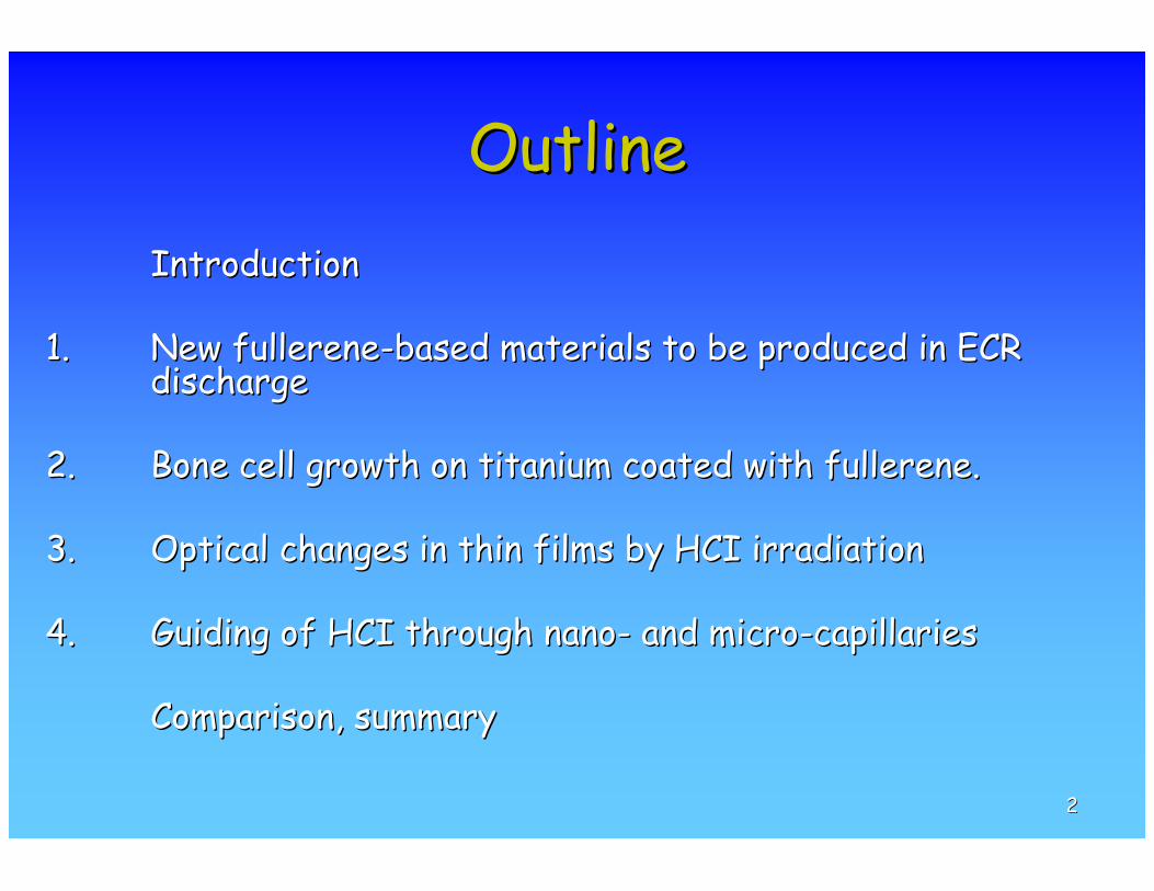
OutlineOutline
IntroductionIntroduction
1.1. New fullereneNew fullerene--based materials to be produced in ECRbased materials to be produced in ECRdischargedischarge
2.2. Bone cell growth on titanium coated withBone cell growth on titanium coated with fullerene.fullerene.
3.3. Optical changes in thin filmsOptical changes in thin films by HCI irradiationby HCI irradiation
4.4. GGuidinguiding of HCI through nanoof HCI through nano-- and microand micro--ccapillarapillariesies
Comparison, summaryComparison, summary

33
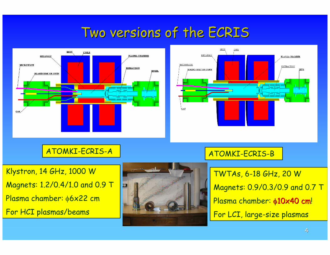
14.14.33 GHz/GHz/11 kWkW AxiAxial fieldal field:1.2/0.4/1.0 T:1.2/0.4/1.0 T RadiRadial fieldal field: 0.9 T: 0.9 T ChamberChamber:: 58x20058x200 ExtractionExtraction: 0.: 0.22--30 KV30 KV
TheThe ATOMKIATOMKI--ECRISECRIS
44
Two versions of the ECRISTwo versions of the ECRIS
TWTAs, 6-18 GHz, 20 W
Magnets: 0.9/0.3/0.9 and 0.7 T
Plasma chamber: 1010xx40 cm40 cm!
For LCI, large-size plasmas
ATOMKI-ECRIS-A ATOMKI-ECRIS-B
Klystron, 14 GHz, 1000 W
Magnets: 1.2/0.4/1.0 and 0.9 T
Plasma chamber: 6x22 cm
For HCI plasmas/beams

55
1. Fullerene1. Fullerene--based new materials (Cbased new materials (C6060+X) to be+X) to beproduced in ECRproduced in ECR--dischargedischarge
Since 2000 fullerene plasmas and beams haveSince 2000 fullerene plasmas and beams havebeen produced at the ATOMKI ECRISbeen produced at the ATOMKI ECRIS
CC6060: just a working material: just a working material(as Ne, Ar, Fe), no(as Ne, Ar, Fe), no „„CC6060 researchresearch””
Production of CProduction of C6060 ion beamion beam(intensity, charge)(intensity, charge)
Fullerene derivatives (destroyingFullerene derivatives (destroying--adding)adding)
Mixture plasmas (CMixture plasmas (C6060+X)+X) New materials (by CNew materials (by C6060+X) to detect+X) to detect
in beamin beam New materials to produce inNew materials to produce in
macroscopic quantitymacroscopic quantity Applications (surface coating, etc.)Applications (surface coating, etc.)

66
Basic C60 experimentsBasic C60 experiments

77
Quantumcomputing High-accuracy
gene diagnosis
Small-sizedelectronic circuit
SuperconductivitySpintronics
High-densitymagneticmemory
High-sensitivityBio sensor
High-efficientorganic
solar cell
Low-powerflat panel display
Nanoscopic Plasma Processes
FullereneFullerene NanotubeNanotube ColloidColloid
Nanocarbon Network
Creation of New-Functional Evolved-Nanomaterials
Next-Generation Information & Nano-Bio Technologies Devices( energy / evaluation / semiconductor / storage / display / bio)
Gaseous Plasmas Solution Plasmas
Slide made by R. Hatakeyama, Tohoku University, Sendai

88
HaHa X=FeX=Fe Fe@CFe@C6060
Nanotechnologynew SC materialsquantum computing
Medical tratmentsultra-contrast Magnetic Resonance Imaging (MRI) agent,magnetic nano-particle
Iron encapsulated in fullerene
In ECR ion sources:In ECR ion sources: Evaporation of CEvaporation of C6060 isis solvedsolved (500 C)(500 C) Production of fullereneProduction of fullerene derivativesderivatives is possibleis possible such as (C60)+, (C58)+, (C56)+,such as (C60)+, (C58)+, (C56)+,……,, (C60)++, (C58)++, (C56)++,(C60)++, (C58)++, (C56)++,……,, Calculations showed that fullerene derivatives areCalculations showed that fullerene derivatives are less stableless stable Therefore we must make aTherefore we must make a twotwo--componentscomponents plasmaplasma 1. component:1. component: CC6060 (mass and charge to be regulated)(mass and charge to be regulated) 2. component:2. component: FeFe: pure iron: pure iron „„gasgas””, positive ions with optimal energy, positive ions with optimal energy Synthesis: volume or surface?Synthesis: volume or surface?
99
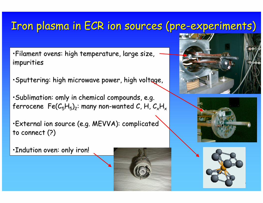
Iron plasma inIron plasma in ECRECR ion sources (preion sources (pre--experiments)experiments)
••Filament ovens: high temperature, large size,Filament ovens: high temperature, large size,impuritiesimpurities
••Sputtering: high microwave power, high voltage,Sputtering: high microwave power, high voltage,
••Sublimation: omly in chemical compounds, e.g.Sublimation: omly in chemical compounds, e.g.ferrocferroceneene Fe(CFe(C55HH55))22:: many nonmany non--wantedwanted C, HC, H, C, CxxHHxx
••External ion sourceExternal ion source ((e.g.e.g. MEVVA):MEVVA): complicatedcomplicatedto connect (?)to connect (?)
••Indution oven: only iron!Indution oven: only iron!

1010
ATOMKI-ECRIS-BHexapole: modified AECR-U
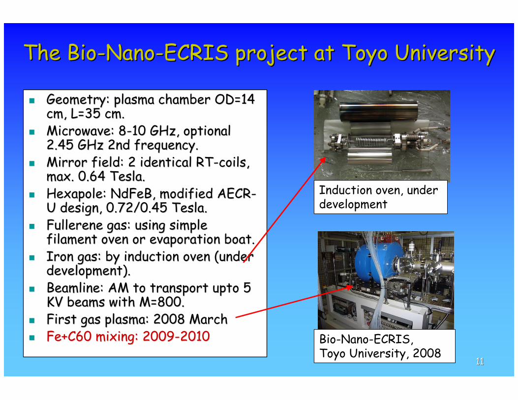
It was decided to build a new ECR ion source at Toyo University,It was decided to build a new ECR ion source at Toyo University, Kawagoe, Japan.Kawagoe, Japan.To produce new, fullereneTo produce new, fullerene--based materials, mainly metalbased materials, mainly metal--encapsulated fullerenes.encapsulated fullerenes.
It is called: BioIt is called: Bio--NanoNano--ECRISECRISCollaborators: Toyo Univ., NIRS, Osaka Univ., Tateyama Co. andCollaborators: Toyo Univ., NIRS, Osaka Univ., Tateyama Co. and ATOMKIATOMKI
1st step: geometry and magnetic trap1st step: geometry and magnetic trap
1111
The BioThe Bio--NanoNano--ECRIS project at Toyo UniversityECRIS project at Toyo University
Geometry:Geometry: plasmaplasma chamber OD=14chamber OD=14cm, L=35 cm.cm, L=35 cm.
Microwave: 8Microwave: 8--10 GHz, optional10 GHz, optional2.45 GHz 2nd frequency.2.45 GHz 2nd frequency.
Mirror field: 2 identical RTMirror field: 2 identical RT--coils,coils,max. 0.64 Tesla.max. 0.64 Tesla.
Hexapole: NdFeB, modified AECRHexapole: NdFeB, modified AECR--U design, 0.72/0.45 Tesla.U design, 0.72/0.45 Tesla.
Fullerene gas: using simpleFullerene gas: using simplefilament oven or evaporation boat.filament oven or evaporation boat.
Iron gas: by induction oven (underIron gas: by induction oven (underdevelopment).development).
Beamline: AM to transport upto 5Beamline: AM to transport upto 5KV beams with M=800.KV beams with M=800.
First gas plasma: 2008 MarchFirst gas plasma: 2008 March Fe+C60 mixing: 2009Fe+C60 mixing: 2009--20102010
Induction oven, underdevelopment
Bio-Nano-ECRIS,Toyo University, 2008

1212
2. Bone cell growth on titanium coated with fullerene.ATOMKI ECRIS Group and Unideb Faculty of Dentistry collaboration
““OOsseointegrationsseointegration””:: bone formation onbone formation on TiTiimplants.implants.EffortsEfforts:: accelerate bone formationaccelerate bone formation,, improveimprovelifetime and mechanical stability.lifetime and mechanical stability.NanotechnologyNanotechnology:: new waysnew ways in implant technicsin implant technicsBBiological usefulness ofiological usefulness of TiTi implants can beimplants can beimprovedimproved byby (1)(1) surfacesurface modificationmodification oror(2) surface(2) surface coatcoatinging..
•Our idea: fullerene (C60) coating as intermediatelayer between metal and organic tissue•C60 ions can be shot to the metal surface with anyrequired velocity: balls remain intact or damaged•fullerene molecules are very reactive: hydroxyl etcother groups can be connected•Such derivatised fullerenes are medically useful•Physical part: to coat titanium surfaces byfullerenes with various velocity and thickness.•Biological tests: growing bone cells on Ti+C60

1313
• Task: irradiate simultaneously 10 Ti samples• Size: 10x10x0.5 mm (d=50 mm beam is necessary)• ATOMKI-ECRIS-B configuration• Primary beamline, 50 cm distance from plasma• 90% of the beam is single-charged• 80% of the extracted beam is fullerene• 90 deg beamline: just composition check• U=250 V and U=500 V extraction voltages• beam accuracy on 5 segments: less than 10% difference• total intensity hit the samples: 300-800 enA• C60 thickness estimated: 1 and 5 layers

1414
321.1250844
874.9250743
231.2500932
904.3500801
Time ofirradiation
(min)
Number of C60molecular layerson the Ti surface
Beamenergy
(eV)
C60fraction inbeam (%)
Tisampleseries
Summary of the Ti coatings by C60

1515
•Human embryonic bone cells were cultured onto the Ti substrates for 48 hours(type: palatal mesenchymal pre-osteoblast, HEPM 1486, ATCC)•Cells dual labeled with special markers (FITC-falloidin), actine and vinculine•Confocal imaging: laser scanning microscope (LSM 510, Carl Zeiss).
Bone cells grown on glass Bone cells grown on Ti+C60 (250 eV)

1616
The morphology of the cells is different compared to the control substrateThe control cells on glass are quite spread showing an interconnected morphologyThe cells grown on the Ti substrates are more spindle-like shape showing denseractine and vinculine structureBut there is no remarkable difference between the four Ti+C60 series, so far.
This first experiment: successfulProved: C60 coating does not prevent bone cells grows.High number of bone cells grew on Ti+C60 (~5*105/cm3)Further experiments: optimal beam properties(energy, rate, density, composition)Goal: improve physical (Ti-C60) and biological (C60-cells) properties
Glass:
Ti+C60:

1717
2004-2006: individual slow ions hitting the surface Amorphous Se layers, 500 nm, on mica Needle-like SbSJ crystals
3. Modificaction of thin films by multiply charged ions
Xe gas natural
•Charge: 20+, 24+
•Ion flux: 1-100 ion/nm2
•Extraction voltage: U= 4…10 KV
0.1
1.0
10.0
100.0
1000.0
0 5 10 15 20 25 30
Xe charge
En
erg
y(K
eV
)
Epot Ekin (U=0.1) Ekin (U=0.5)
Ekin (U=2) Ekin (U=10)

1818
Surface structuringSurface structuring –– AFM photosAFM photos
Production of surfacemicro and nanostructuresin one step without etching
Xe20...24+
E= 120-240 keV
One possible mechanism of nano-hillock formation consists in theprocess, similar to the radiation-stimulated creation and diffusion ofdefects to the drains at the surface.
Hillocks!

1919
20072007--2008: volume effects2008: volume effects
Ions: NeIons: Neq+q+ (q=4...8)(q=4...8) EEkinkin= 120 keV fixed= 120 keV fixed Sample: AsSe layer on glassSample: AsSe layer on glass d=700 nmd=700 nm Penetration depth R= 200 nmPenetration depth R= 200 nm Measured parameter:Measured parameter: darkeningdarkening
(T/T(T/T00) depending on the charge) depending on the charge
550 600 650 7000
20
40
60
80
100
T,%
, nm
constRaRdaRaadTT )exp())(exp()exp()exp(/ 110
550 600 650 7000
20
40
60
80
100
T,%
, nm
Precedents
•Laser induced structural changes
•Ion irradiation induced structuralchanges (H+, D+)
•As2S3 , AsSe, Se

2020
0 2 4 6 8 10 12 14
0.0
0.2
0.4
0.6
0.8
1.0
600 nm
4+5+6+8+
T/T
0
fluence, ion/cm2
-2 0 2 4 6 8 10 12 14
0.2
0.4
0.6
0.8
1.0 640 nm4+5+6+8+
T/T
0
fluens, 1014 ion/cm2
3 4 5 6 7 8 90.6
0.7
0.8
0.9
1.0
1.1
R
,rel
.uni
ts
charge state
Our experiment showed that(T/T0)sat is larger for the sampleirradiated with Ne8+ ions than forthe one irradiated with Ne4+ ions.
Global optical property can beeffected by the charge!

2121
Scattering Region ΔαGuiding Region
10 µm
100 nm
4. Guiding of slow, highly charged ions through nano-capillaries
Ions with few keV energy have been transmitted through capillaries of thin PETand SiO2 insulating foilsThere was significant transmission even if the capillaries were tilted by largeangles, i.e., when there is no geometrical transparency for straight line trajectories.The initial charge state may be or may be not changed.
Prospective applications:
- ion guiding, directing, focusing slow ion beamsin nanoscale devices.
- they might be used for irradiating single cellsand writing on charge sensitive surfaces

2222
2004-2008: ATOMKI-ECRIS-A Target: membranes of nanochanneled
Al2O3, thickness 15 μm, honeycomb capillary diameters: 140-260 nm to prevent charging up: 20 nm Nb layers Neon (6+, 7+), argon (8+, 9+) Extraction: 500 V Beam: two 1 mm diaphragms at 205 mm Beam current 300-500 pA Detectors: FC, ion-spectrometer
(channeltron), multi-channel-plate (MCP)

2323
Ion beam
Capillary array
Spectrometer,MCP detectoror Faraday cup
Experimentalsetup

2424
Deflector plates
+
+-
-
Ion beam
Photons
~ 4 mm
Sample
0.5 1 1.5 2 2.5 3
10
100
1000
Inte
nsity
(arb
.uni
ts)
Ion energy/Charge (keV)
Sample: Al2O3, d=140 nm
Tilt angle: 0o
Ne1+Ne2+
Ne3+
Ne4+
Ne5+
Ne6+
-10 -5 0 5 101E-3
0.01
0.1
1
10 Angular distributions at different tilt anglesTarget: 290 nm Al
2O
3
Nor
mal
ized
coun
ts/s
Observation angle (degree)
5o
2.5o
0o
-2.50
-5o
Primary Beam Results
The capillary guiding works !Ion CSD afterthe capilleriesUV photons were
generated in theAM chamber
Deflector+MCPcan separate them

2525
Comparison and summary
Puller on highnegative voltage
Beams with sametotal energy
Irradiation in thezero-degree
beamline
Synthesis inplasma or on
surface
Specification:
200-600200-4004-201-50Microwavepower (W)
14.314.312-148-12Microwavefrequency (GHz)
500-100015000-30000250-500500-5000Extractionvoltage (V)
145010-20Beam diameter(mm)
Ne6+,7+, Ar8+,9+Ne4+…8+C60+Fe+, C60
+Plasma/beam:
ATOMKI-ECRIS-AATOMKI-ECRIS-AATOMKI-ECRIS-BATOMKI-ECRIS-Band Bio-Nano-ECRIS
Ion source:
Capillaryguiding
Thin layermodification
Ti implantscoating
Endohedralfullerenes
Projectshort name:
The tasks and beam requirements were different, but the ECR source proved to be versatileenough to fulfill all these jobs and serves as a very useful multi-purpose facility.

2626
Thank you for your attention!Thank you for your attention!