Application Note: Using Modbus With the Conext™...
28
‘ Overview Modbus is a simple and robust open communication protocol used to provide interoperability between products from many different vendors. The purpose of this Application Note is to provide a brief overview of the Modbus hardware and software support on Conext Core XC Series inverters so that you can quickly and easily interface the inverter with any third-party Modbus devices. The inverter performs Modbus communications according to the Modbus Application Protocol v1.1b. It is assumed that you are familiar with the Modbus protocol and with serial communications in general. The Vigilohm® IM400 insulation monitoring device, which is used only in ungrounded (floating) systems, is configured as a Modbus slave and has its own Modbus address and a separate Modbus map. For more information, see “Vigilohm IM400 Device Modbus Map” on page 27. Application Note: Using Modbus With the Conext™ Core XC Series AP-XC-004-EN Rev E WARNING l LOSS OF CONTROL The designer of any control scheme must consider the potential failure modes of control paths and, for certain critical control functions, provide a means to achieve a safe state during and after a path failure. An example of a critical control function is emergency stop. Separate or redundant control paths must be provided for critical control functions. System control paths may include communication links. Consideration must be given to the implications of anticipated transmission delays or failures of the link. Each implementation of Modbus control over a Conext Core XC Series inverter must be individually and thoroughly tested for proper operation before being placed into service. Failure to follow these instructions can result in death, serious injury, or equipment damage.
Transcript of Application Note: Using Modbus With the Conext™...

‘
Overview
Modbus is a simple and robust open communication protocol used to provide interoperability between products from many different vendors. The purpose of this Application Note is to provide a brief overview of the Modbus hardware and software support on Conext Core XC Series inverters so that you can quickly and easily interface the inverter with any third-party Modbus devices.
The inverter performs Modbus communications according to the Modbus Application Protocol v1.1b. It is assumed that you are familiar with the Modbus protocol and with serial communications in general.
The Vigilohm® IM400 insulation monitoring device, which is used only in ungrounded (floating) systems, is configured as a Modbus slave and has its own Modbus address and a separate Modbus map. For more information, see “Vigilohm IM400 Device Modbus Map” on page 27.
Application Note: Using Modbus With the Conext™ Core XC Series
AP-XC-004-ENRev E
WARNINGl
LOSS OF CONTROL
The designer of any control scheme must consider the potential failure modes of control paths and, for certain critical control functions, provide a means to achieve a safe state during and after a path failure. An example of a critical control function is emergency stop.Separate or redundant control paths must be provided for critical control functions.System control paths may include communication links. Consideration must be given to the implications of anticipated transmission delays or failures of the link.Each implementation of Modbus control over a Conext Core XC Series inverter must be individually and thoroughly tested for proper operation before being placed into service.
Failure to follow these instructions can result in death, serious injury, or equipment damage.

Using Modbus With the Conext Core XC Series
2 AP-XC-004-EN Rev E
Inverter Modbus Specifications
The Conext Core XC Series meets the following Modbus specifications:
• The inverter is capable of communicating via the RS-485 serial communication standard. The RS-485 medium allows for multiple devices on the same serial bus network.
• The inverter’s serial interface meets the specifications outlined in the Modbus over Serial Line Specification and Implementation Guide, version 1.02.
• All communications on the network conform to a master/slave scheme. In this scheme, information and data are transferred between a Modbus master device and up to 253 slave devices.
• The master device initiates and controls all information transfer on the Modbus serial bus network.
• A slave device never initiates a communication sequence, and must remain silent unless addressed specifically by the master.
• The Conext Core XC Series is a Modbus slave device.
• All packets transmitted by the master are requests. All packets transmitted by a slave are responses.
• At most, one slave can respond to a single request from a master.
• Each Modbus network only has one master.
• The Modbus protocol supports RTU and ASCII protocols. The Conext Core XC Series supports only the Modbus/RTU protocol.
Related Documents
The following related documents are available from www.modbus.org:
• MODBUS Read Device Identification Extension (FC 43/14), RFC TR_026, version 0.8
• MODBUS Application Protocol Specification, version 1.1b
• MODBUS over Serial Line Specification and Implementation Guide, version 1.02
WARNING
LOSS OF CONTROL
Do not assign the same address to two Modbus devices. The entire serial bus may behave unexpectedly if the master device cannot communicate with all the slave devices on the bus.
Failure to follow these instruction can result in death, serious injury, or equipment damage.
Using Modbus With the Conext Core XC Series
AP-XC-004-EN Rev E 3
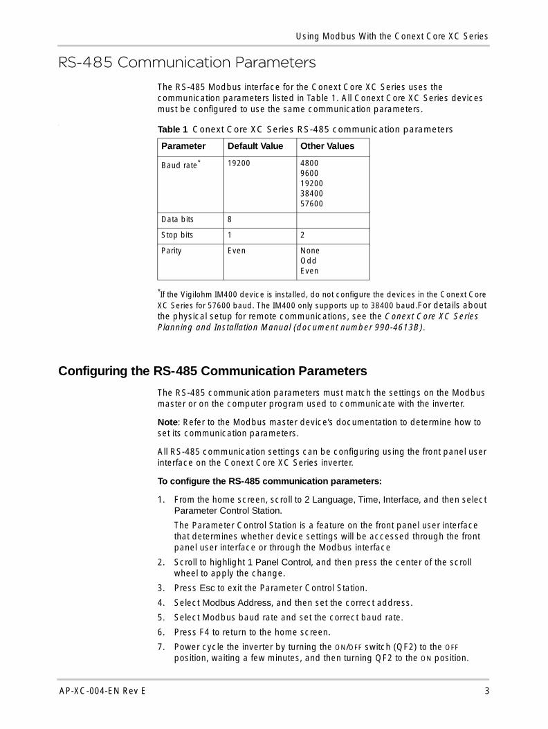
RS-485 Communication ParametersThe RS-485 Modbus interface for the Conext Core XC Series uses the communication parameters listed in Table 1. All Conext Core XC Series devices must be configured to use the same communication parameters.
F
*If the Vigilohm IM400 device is installed, do not configure the devices in the Conext Core XC Series for 57600 baud. The IM400 only supports up to 38400 baud.For details about the physical setup for remote communications, see the Conext Core XC Series Planning and Installation Manual (document number 990-4613B).
Configuring the RS-485 Communication Parameters
The RS-485 communication parameters must match the settings on the Modbus master or on the computer program used to communicate with the inverter.
Note: Refer to the Modbus master device’s documentation to determine how to set its communication parameters.
All RS-485 communication settings can be configuring using the front panel user interface on the Conext Core XC Series inverter.
To configure the RS-485 communication parameters:
1. From the home screen, scroll to 2 Language, Time, Interface, and then select Parameter Control Station.
The Parameter Control Station is a feature on the front panel user interface that determines whether device settings will be accessed through the front panel user interface or through the Modbus interface
2. Scroll to highlight 1 Panel Control, and then press the center of the scroll wheel to apply the change.
3. Press Esc to exit the Parameter Control Station.
4. Select Modbus Address, and then set the correct address.
5. Select Modbus baud rate and set the correct baud rate.
6. Press F4 to return to the home screen.
7. Power cycle the inverter by turning the ON/OFF switch (QF2) to the OFF position, waiting a few minutes, and then turning QF2 to the ON position.
Table 1 Conext Core XC Series RS-485 communication parameters
Parameter Default Value Other Values
Baud rate* 19200 48009600192003840057600
Data bits 8
Stop bits 1 2
Parity Even NoneOddEven
Using Modbus With the Conext Core XC Series
4 AP-XC-004-EN Rev E
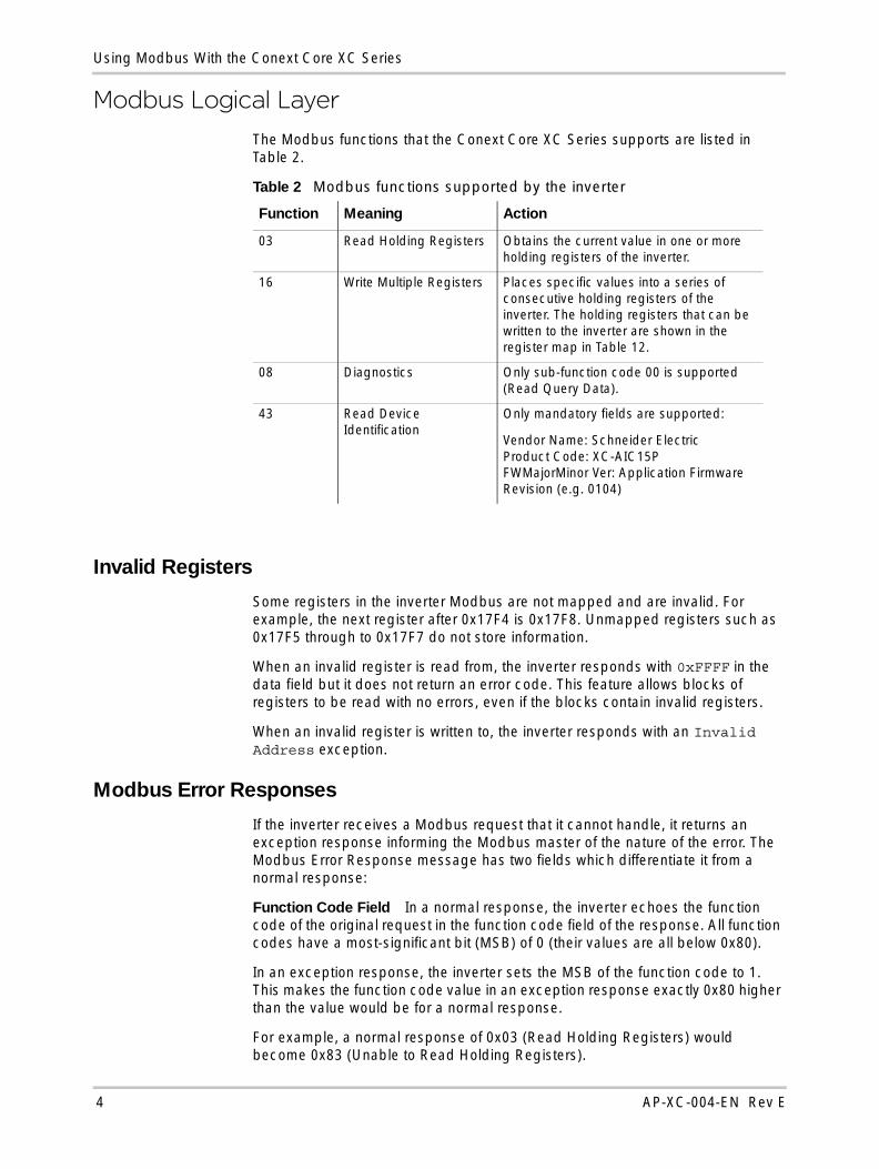
Modbus Logical LayerThe Modbus functions that the Conext Core XC Series supports are listed in Table 2.
Invalid Registers
Some registers in the inverter Modbus are not mapped and are invalid. For example, the next register after 0x17F4 is 0x17F8. Unmapped registers such as 0x17F5 through to 0x17F7 do not store information.
When an invalid register is read from, the inverter responds with 0xFFFF in the data field but it does not return an error code. This feature allows blocks of registers to be read with no errors, even if the blocks contain invalid registers.
When an invalid register is written to, the inverter responds with an Invalid Address exception.
Modbus Error Responses
If the inverter receives a Modbus request that it cannot handle, it returns an exception response informing the Modbus master of the nature of the error. The Modbus Error Response message has two fields which differentiate it from a normal response:
Function Code Field In a normal response, the inverter echoes the function code of the original request in the function code field of the response. All function codes have a most-significant bit (MSB) of 0 (their values are all below 0x80).
In an exception response, the inverter sets the MSB of the function code to 1. This makes the function code value in an exception response exactly 0x80 higher than the value would be for a normal response.
For example, a normal response of 0x03 (Read Holding Registers) would become 0x83 (Unable to Read Holding Registers).
Table 2 Modbus functions supported by the inverter
Function Meaning Action
03 Read Holding Registers Obtains the current value in one or more holding registers of the inverter.
16 Write Multiple Registers Places specific values into a series of consecutive holding registers of the inverter. The holding registers that can be written to the inverter are shown in the register map in Table 12.
08 Diagnostics Only sub-function code 00 is supported (Read Query Data).
43 Read Device Identification
Only mandatory fields are supported:
Vendor Name: Schneider ElectricProduct Code: XC-AIC15PFWMajorMinor Ver: Application Firmware Revision (e.g. 0104)

Using Modbus With the Conext Core XC Series
AP-XC-004-EN Rev E 5
Data Field In an error response, the inverter uses the data field of the response packet to return an error code to the Modbus master. The error codes that are supported are listed in Table 3.
Operational Mode State Codes (0x1700)
Register 0x1700 is a 16-bit code where:
• MS-Byte contains the Enable Mode of the system (Modbus Register 0xEFFC).
• LS-Byte contains the state for that Enable Mode.
Register 0x1700 has the characteristics listed in Table 4.
Table 3 Modbus error codes
Error Code Error Name Description
01 Illegal Function The inverter does not support the function code specified in the Modbus Request Packet.
02 Illegal Address The address range specified in the Modbus Request Packet contains an illegal register address.
04 Diagnostics Only sub-function code 00 is supported (Read Query Data).
43 Slave Device Failure An unrecoverable error occurred while the server (or slave) was attempting to perform the requested action.
Table 4 Register 0x1700
Enable CodeEnable Operational State Code
PV Mode Offline 0x0000
Reconnecting 0x0001
Online 0x0002
CP Mode Offline 0x0100
Reconnecting 0x0101
Online 0x0102
PVCQ Mode Offline 0x0200
Reconnecting 0x0201
Online 0x0202
Grid Online 0x0203
Using Modbus With the Conext Core XC Series
6 AP-XC-004-EN Rev E
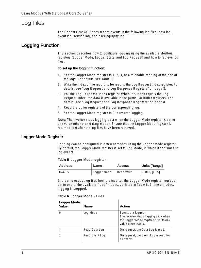
Log FilesThe Conext Core XC Series record events in the following log files: data log, event log, service log, and oscillography log.
Logging Function
This section describes how to configure logging using the available Modbus registers (Logger Mode, Logger State, and Log Request) and how to retrieve log files.
To set up the logging function:
1. Set the Logger Mode register to 1, 2, 3, or 4 to enable reading of the one of the logs. For details, see Table 6.
2. Write the index of the record to be read to the Log Request Index register. For details, see “Log Request and Log Response Registers” on page 8.
3. Poll the Log Response Index register. When this index equals the Log Request Index, the data is available in the particular buffer registers. For details, see “Log Request and Log Response Registers” on page 8.
4. Read the buffer registers of the corresponding log.
5. Set the Logger Mode register to 0 to resume logging.
Note: The inverter stops logging data when the Logger Mode register is set to any value other than 0 (Log mode). Ensure that the Logger Mode register is returned to 0 after the log files have been retrieved.
Logger Mode Register
Logging can be configured in different modes using the Logger Mode register. By default, the Logger Mode register is set to Log Mode, in which it continues to log events.
In order to extract log files from the inverter, the Logger Mode register must be set to one of the available “read” modes, as listed in Table 6. In these modes, logging is stopped.
Table 5 Logger Mode register
Address Name Access Units [Range]
0x4705 Logger mode Read/Write Uint16, [0...5]
Table 6 Logger Mode values
Logger Mode Value Name Action
0 Log Mode Events are logged. The inverter stops logging data when the Logger Mode register is set to any value other than 0.
1 Read Data Log On request, the Data Log is read.
2 Read Event Log On request, the Event Log is read for all events.
Using Modbus With the Conext Core XC Series
AP-XC-004-EN Rev E 7
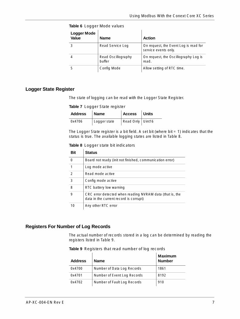
Logger State Register
The state of logging can be read with the Logger State Register.
The Logger State register is a bit field. A set bit (where bit = 1) indicates that the status is true. The available logging states are listed in Table 8.
Registers For Number of Log Records
The actual number of records stored in a log can be determined by reading the registers listed in Table 9.
3 Read Service Log On request, the Event Log is read for service events only.
4 Read Oscillography buffer
On request, the Oscillography Log is read.
5 Config Mode Allow setting of RTC time.
Table 6 Logger Mode values
Logger Mode Value Name Action
Table 7 Logger State register
Address Name Access Units
0x4706 Logger state Read Only Uint16
Table 8 Logger state bit indicators
Bit Status
0 Board not ready (init not finished, communication error)
1 Log mode active
2 Read mode active
3 Config mode active
8 RTC battery low warning
9 CRC error detected when reading NVRAM data (that is, the data in the current record is corrupt)
10 Any other RTC error
Table 9 Registers that read number of log records
Address NameMaximum Number
0x4700 Number of Data Log Records 1861
0x4701 Number of Event Log Records 8192
0x4702 Number of Fault Log Records 910

Using Modbus With the Conext Core XC Series
8 AP-XC-004-EN Rev E
No register exists to read the number of oscillography records—there are always 500 oscillography records.
Log Request and Log Response Registers
The reading of logs can be configured using the Log Request Index and Log Response Index registers.
Log Request Index
The Log Request Index register is limited to the maximum number of records in the event log. When the Logger Mode register is written, the Log Request Index register must be reset to 0. The Log Request Index register is only writeable when the Logger Mode register is configured to one of the read modes.
• Index 0 means that nothing is to be read from the Logger.
• Index 1 means that the most recent record of the event log is to be read.
Log Response Index
The value in the Log Response Index register is set to the same value as the Log Request Index as soon as the data is available in the corresponding buffer registers. This register should be polled until the expected value is read.
Timestamps
The event, service and data logs contain timestamps. Timestamps can be converted to time using the following formula:
(TimestampHigh * 65536) + TimestampLow + (Timestamp ms / 1000)
Data Logs
Data logs contain measurement and state information that is used for troubleshooting. By default, this information is logged every 5 minutes. Only Schneider Electric personnel may change this rate.
Data logs can be obtained by reading the registers listed in Table 11.
Table 10 Log Request and Log Response registers
Address Name Access Units [Range]
0x4703 Log Request Index Read/Write Uint16, [0...Idx_max]
0x4704 Log Response Index Read Only Uint16, [0...Idx_max]
Table 11 Data log registers
Address Name Access Units/Range
0x4811 Timestamp High Read Only uint16, most significant bit in Unix format (starting on 01.01.1970)
0x4812 Timestamp Low Read Only uint16, least significant bit in Unix format (starting on 01.01.1970

Using Modbus With the Conext Core XC Series
AP-XC-004-EN Rev E 9
0x4813 kWh Energy High Read Only Most significant word of kWh Energy
0x4814 kWh Energy Low Read Only Least significant word of kWh Energy
0x4815 Grid AC voltage phase A to phase B, RMS
Read Only Sint16, 0.1V
0x4816 Grid AC voltage phase B to phase C, RMS
Read Only Sint18, 0.1V
0x4817 Grid AC voltage phase C to phase A, RMS
Read Only Sint16, 0.1V
0x4818 Inverter AC Current Phase A, RMS
Read Only Sint16, 0.1A
0x4819 Inverter AC Current Phase B, RMS
Read Only Sint16, 0.1A
0x481A Inverter AC Current Phase C, RMS
Read Only Sint16, 0.1A
0x481B Grid frequency Read Only Sint16, 0.1Hz
0x481C Real power Read Only Sint16, kW
0x481D Reactive power Read Only Sint16, kVAr
0x481E DC bus voltage Read Only Sint16, 0.1V
0x481F PV voltage Read Only Sint16, 0.1V
0x4820 PV current Read Only Sint16, 0.1A
0x4821 PV power Read Only Sint16, 0.1kW
0x4822 Ground current Read Only Sint16, 0.1A
0x4823 Normalized thermal numbers
Read Only Uint16,%, [1....112]
0x4824 APP-Info1 (see page 11) Read Only Uint16
0x4825 APP-Info 2 (see page 12) Read Only Uint16
0x4826 APP-Info 3 (see page 12) Read Only Uint18
0x4827 APP-Info 4 (see page 12) Read Only Uint16
0x4828 DC voltage reference Read Only Sint16, 0.1V
0x4829 Power reference Read Only Sint16, kW
0x482A Reactive power reference Read Only Sint16, kVAr
0x482B PV power by slave 1 (paralleling mode)
Read Only Sint16, kW
0x482C PV power by slave 2 (paralleling mode)
Read Only Sint16, kW
0x482D Highest priority event code Read Only Uint16
0x482E Power Point Shifting Flag Read Only Uint16
Table 11 Data log registers
Address Name Access Units/Range

Using Modbus With the Conext Core XC Series
10 AP-XC-004-EN Rev E
Oscillography Logs
Oscillography logs contain 500 sets of measurement and state information that are captured at 1ms. Of these 500 data sets, 250 sets are captured before the last service event and 250 after the last service event.
Oscillography logs can be obtained by reading the registers listed in Table 12.
Event Logs
All inverter events, including service events, are stored in the event logs. All events are stored whenever they occur, at a maximum rate of four events every 1.5ms. Event logs are time-stamped with a resolution of one millisecond.
The event log can store a maximum of four simultaneous events (where 0 is not an event code). If fewer than 4 events happen at the same time, valid events are non-zero and invalid events are zero.
The event log content can be obtained by reading the registers listed in Table 13 on page 11.
Table 12 Oscillography log registers
Address Name Access Units/Range
0x4646 Oscillography Item 1 (Vab) Read Only Sint16, 0.1V
0x4647 Oscillography Item 2 (Vbc) Read Only Sint16, 0.1V
0x4648 Oscillography Item 3 (Vca) Read Only Sint16, 0.1V
0x4649 Oscillography Item 4 (Ia) Read Only Sint16, 0.1A
0x464A Oscillography Item 5 (Ib) Read Only Sint16, 0.1A
0x464B Oscillography Item 6 (Ic) Read Only Sint16, 0.1A
0x464C Oscillography Item 7 (Vpv) Read Only Sint16, 0.1V
0x464D Oscillography Item 8 (Ipv) Read Only Sint16, 0.1A
0x464E Oscillography Item 9 (Ignd) Read Only Sint16, 0.1A
0x464F Oscillography Item 10 (Vdc) Read Only Sint16, 0.1V
0x46450 Oscillography Item 11 (APP-Info 1) (see page 11)
Read Only Uint16
0x46451 Oscillography Item 12 (APP-Info 2) (see page 12)
Read Only Uint16
0x46452 Oscillography Item 13 (APP-Info 3) (see page 12)
Read Only Uint16
0x46453 Oscillography Item 14 (APP-Info 4) (see page 12)
Read Only Uint16
0x46454 Oscillography Item 15; reserved Read Only Uint16
0x46455 Oscillography Item 16; reserved Read Only Uint16
0x46456 Oscillography Item 17; reserved Read Only Uint16

Using Modbus With the Conext Core XC Series
AP-XC-004-EN Rev E 11
Service Logs
Service events are a special case of the more general term “events”. Service events are stored in the service log whenever they occur, at a maximum rate of four service events every 1.5 ms. Service logs are time-stamped with a resolution of one millisecond.
The service log can store a maximum of four simultaneous events (where 0 is not an event code). If fewer than 4 events happen at the same time, valid events are non-zero and invalid events are zero.
The service log content can be obtained by reading the registers listed in Table 14.
App-Info
App-Info defines information from the data logs and oscillography on the Application (APP) board.
App-Info1
App-Info 1 has the same codes as Register 0x1700 (see “Operational Mode State Codes (0x1700)” on page 5).
Table 13 Event log registers
Address Name Access Units/Range
0x4720 Timestamp High Read Only Uint32, Unix format(starting on 01.01.1970)
0x4721 Timestamp Low Read Only Uint32, Unix format(starting on 01.01.1970)
0x4722 Timestamp ms Read Only Uint16, ms, [0..999]
0x4723 Event 1 Read Only Uint16
0x4724 Event 2 Read Only Uint16
0x4725 Event 3 Read Only Uint16
0x4726 Event 4 Read Only Uint16
Table 14 Service log registers
Address Name Access Units/Range
0x4740 Timestamp High Read Only Uint32, Unix format(starting on 01.01.1970)
0x4741 Timestamp Low Read Only Uint32, Unix format(starting on 01.01.1970)
0x4742 Timestamp ms Read Only Uint16, ms, [0..999]
0x4743 Fault Read Only Uint16
Using Modbus With the Conext Core XC Series
12 AP-XC-004-EN Rev E
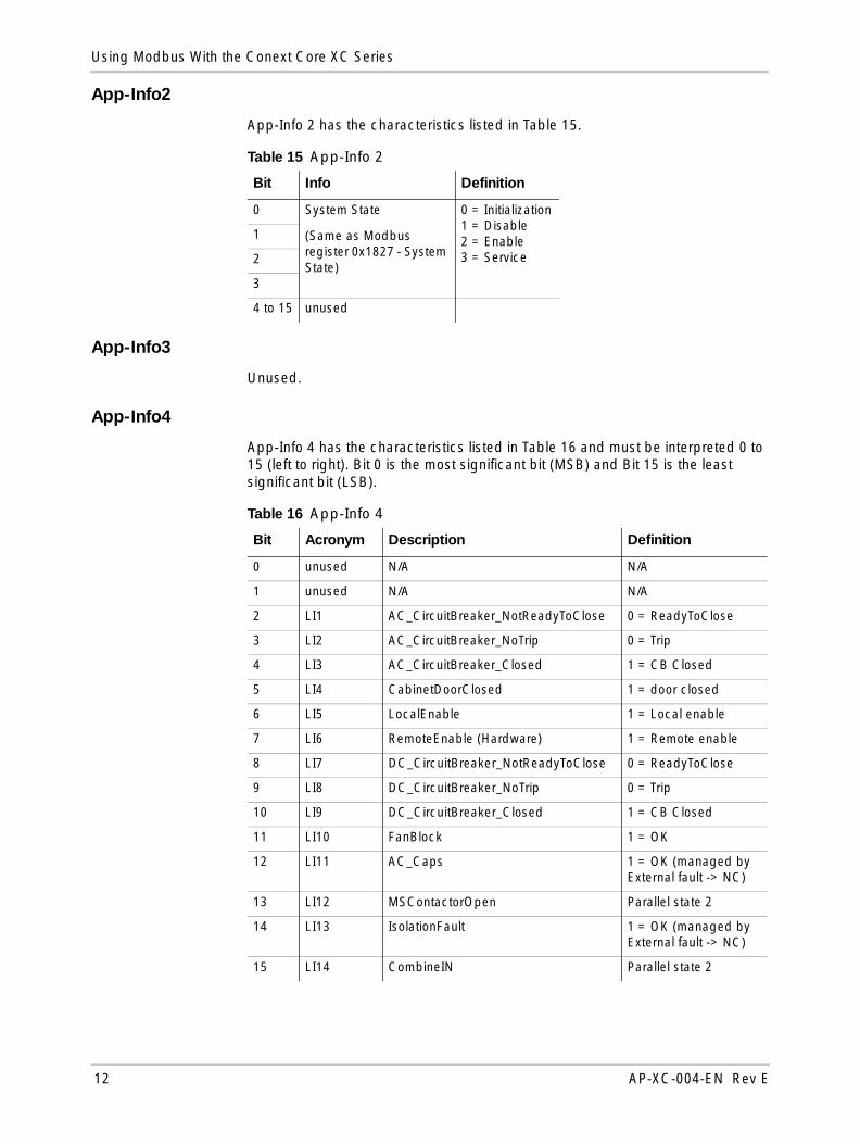
App-Info2
App-Info 2 has the characteristics listed in Table 15.
App-Info3
Unused.
App-Info4
App-Info 4 has the characteristics listed in Table 16 and must be interpreted 0 to 15 (left to right). Bit 0 is the most significant bit (MSB) and Bit 15 is the least significant bit (LSB).
Table 15 App-Info 2
Bit Info Definition
0 System State
(Same as Modbus register 0x1827 - System State)
0 = Initialization1 = Disable2 = Enable3 = Service
1
2
3
4 to 15 unused
Table 16 App-Info 4
Bit Acronym Description Definition
0 unused N/A N/A
1 unused N/A N/A
2 LI1 AC_CircuitBreaker_NotReadyToClose 0 = ReadyToClose
3 LI2 AC_CircuitBreaker_NoTrip 0 = Trip
4 LI3 AC_CircuitBreaker_Closed 1 = CB Closed
5 LI4 CabinetDoorClosed 1 = door closed
6 LI5 LocalEnable 1 = Local enable
7 LI6 RemoteEnable (Hardware) 1 = Remote enable
8 LI7 DC_CircuitBreaker_NotReadyToClose 0 = ReadyToClose
9 LI8 DC_CircuitBreaker_NoTrip 0 = Trip
10 LI9 DC_CircuitBreaker_Closed 1 = CB Closed
11 LI10 FanBlock 1 = OK
12 LI11 AC_Caps 1 = OK (managed by External fault -> NC)
13 LI12 MSContactorOpen Parallel state 2
14 LI13 IsolationFault 1 = OK (managed by External fault -> NC)
15 LI14 CombineIN Parallel state 2

Using Modbus With the Conext Core XC Series
AP-XC-004-EN Rev E 13
Conext Core XC Series Modbus MapRegister addresses in the Modbus map are zero based and are specified in hexadecimal notation. These addresses correspond directly with the address field specified in the Modbus Request Packet, making it easier to troubleshoot when capturing data “over-the-wire”.
If you need to enter these address values into the data definition file of a Modbus master device that is expecting a register number, you must convert the address to decimal (base 10) format and add 1 to the address.
Register Unit Scale
All numbers that are sent or received using Modbus communication are integers. The Modbus registers use a scaling factor so that numbers can be sent and received that are smaller than 1.
For example, if the unit scale is x10, you would divide the Modbus register value by 10 to convert it to a real world value.
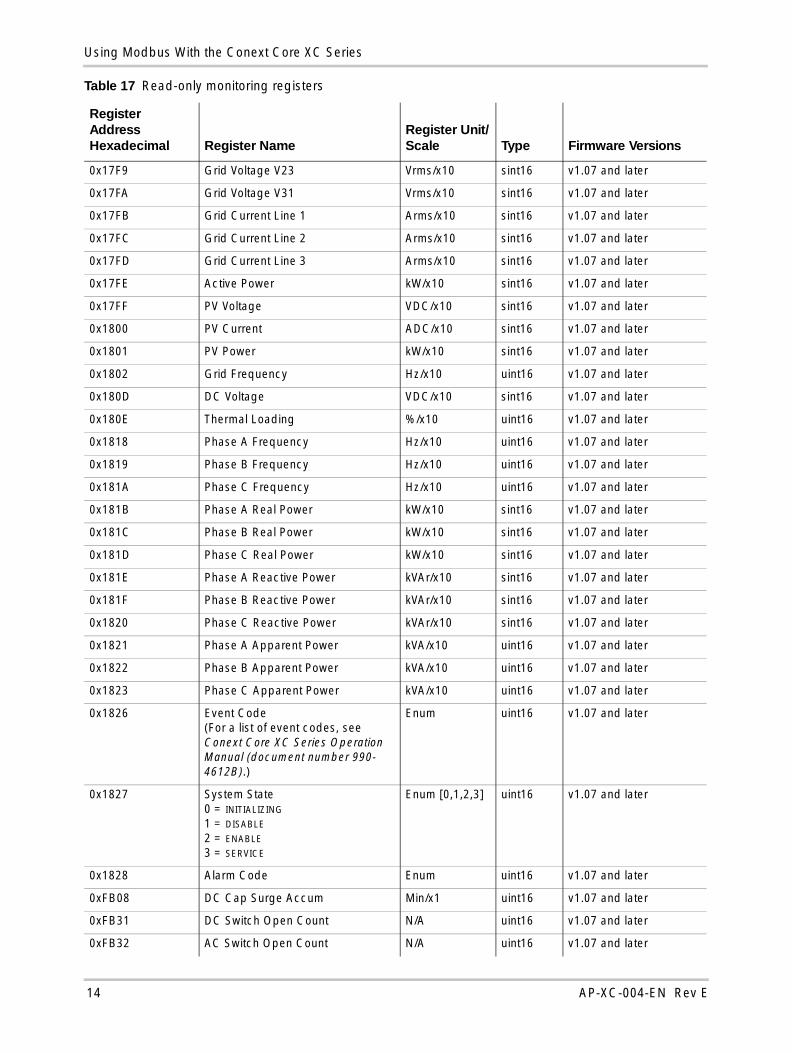
Read-Only Monitoring Registers
Read-only monitoring registers capture the changing status of the inverter, as described in Table 17.
Table 17 Read-only monitoring registers
Register Address Hexadecimal Register Name
Register Unit/Scale Type Firmware Versions
0x1-0x9 Product Model Designation N/A uchar8 v1.07 and later
0xA-0x13 Finished Goods Assembly Number N/A uchar8 v1.07 and later
0x14-0x1D Product Serial Number N/A uchar8 v1.07 and later
0x001E-0x0027 Software Part Number N/A uchar8 v1.07 and later
0x0802-0x0803 kWh Energy Produced kWhr/x10 uint32 v1.07 and later
0x0804-0x0805 Energy Today kWhr/x10 uint32 v1.07 and later
0x081E-0x081F Operating Hours Hours/x1 uint32 v1.07 and later
0x1700 Operational Mode State(For details, see “Operational Mode State Codes (0x1700)” on page 5.)
Enum uint16 v1.07 and later
0x1701 Temperature Power Board C/x10 sint16 v1.07 and later
0x1702 Temperature Heatsink 1 C/x10 sint16 v1.07 and later
0x1703 Temperature Heatsink 2 C/x10 sint16 v1.07 and later
0x1704 Temperature Heatsink 3 C/x10 sint16 v1.07 and later
0x1705 Grid Current Arms/x10 sint16 v1.07 and later
0x17F1 Apparent Power kVA/x10 uint16 v1.07 and later
0x17F4 Reactive Power kVAr/x10 sint16 v1.07 and later
0x17F8 Grid Voltage V12 Vrms/x10 sint16 v1.07 and later
Using Modbus With the Conext Core XC Series
14 AP-XC-004-EN Rev E
0x17F9 Grid Voltage V23 Vrms/x10 sint16 v1.07 and later
0x17FA Grid Voltage V31 Vrms/x10 sint16 v1.07 and later
0x17FB Grid Current Line 1 Arms/x10 sint16 v1.07 and later
0x17FC Grid Current Line 2 Arms/x10 sint16 v1.07 and later
0x17FD Grid Current Line 3 Arms/x10 sint16 v1.07 and later
0x17FE Active Power kW/x10 sint16 v1.07 and later
0x17FF PV Voltage VDC/x10 sint16 v1.07 and later
0x1800 PV Current ADC/x10 sint16 v1.07 and later
0x1801 PV Power kW/x10 sint16 v1.07 and later
0x1802 Grid Frequency Hz/x10 uint16 v1.07 and later
0x180D DC Voltage VDC/x10 sint16 v1.07 and later
0x180E Thermal Loading %/x10 uint16 v1.07 and later
0x1818 Phase A Frequency Hz/x10 uint16 v1.07 and later
0x1819 Phase B Frequency Hz/x10 uint16 v1.07 and later
0x181A Phase C Frequency Hz/x10 uint16 v1.07 and later
0x181B Phase A Real Power kW/x10 sint16 v1.07 and later
0x181C Phase B Real Power kW/x10 sint16 v1.07 and later
0x181D Phase C Real Power kW/x10 sint16 v1.07 and later
0x181E Phase A Reactive Power kVAr/x10 sint16 v1.07 and later
0x181F Phase B Reactive Power kVAr/x10 sint16 v1.07 and later
0x1820 Phase C Reactive Power kVAr/x10 sint16 v1.07 and later
0x1821 Phase A Apparent Power kVA/x10 uint16 v1.07 and later
0x1822 Phase B Apparent Power kVA/x10 uint16 v1.07 and later
0x1823 Phase C Apparent Power kVA/x10 uint16 v1.07 and later
0x1826 Event Code(For a list of event codes, see Conext Core XC Series Operation Manual (document number 990-4612B).)
Enum uint16 v1.07 and later
0x1827 System State0 = INITIALIZING
1 = DISABLE
2 = ENABLE
3 = SERVICE
Enum [0,1,2,3] uint16 v1.07 and later
0x1828 Alarm Code Enum uint16 v1.07 and later
0xFB08 DC Cap Surge Accum Min/x1 uint16 v1.07 and later
0xFB31 DC Switch Open Count N/A uint16 v1.07 and later
0xFB32 AC Switch Open Count N/A uint16 v1.07 and later
Table 17 Read-only monitoring registers
Register Address Hexadecimal Register Name
Register Unit/Scale Type Firmware Versions

Using Modbus With the Conext Core XC Series
AP-XC-004-EN Rev E 15
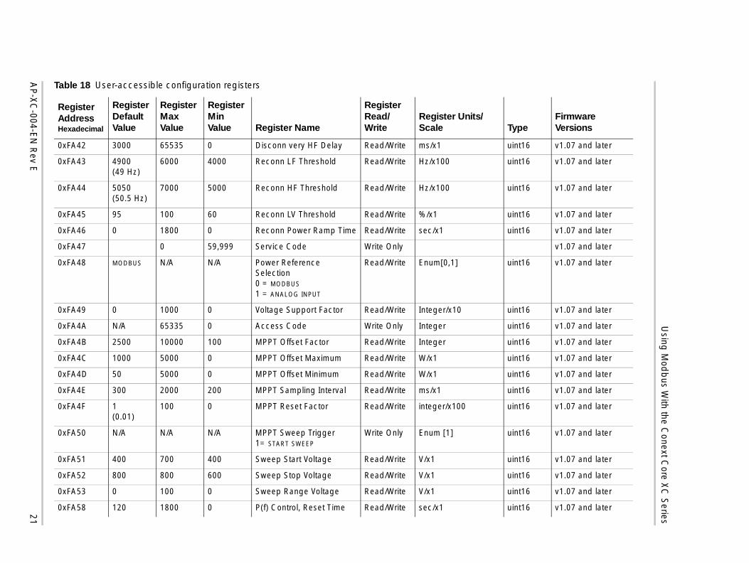
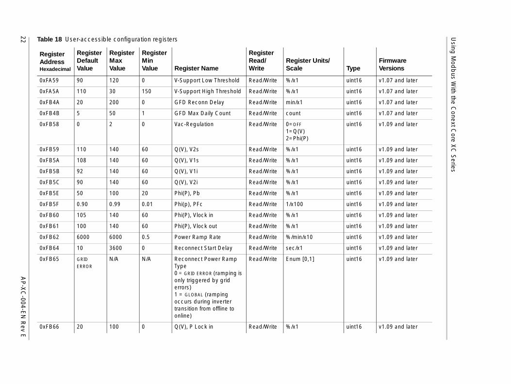
User-Accessible Configuration Registers
User-accessible configuration registers can be changed by the user and are not password protected. The registers are described in Table 18 on page 17. When you change a register value marked with * in Table 18, you must reset the system (that is, turn the inverter off and then on) before the change takes effect.
You must disable the inverter (locally or remotely) before most registers can be changed. Only registers marked with ** in Table 18 can be changed while the inverter is enabled.
To change register values remotely using Modbus:
1. Change parameter control from the front panel user interface to Modbus by writing 2 (Modbus) to register 0xE0E0 (see Table 18 on page 17).
2. Disable the inverter by writing 1 (remote shutdown) to register 0xEFFE (see Table 18 on page 17).
3. Make changes to the register values as required.
4. When all the required changes are complete, return parameter control back to the front panel user interface by writing 1 (panel control) to register 0xE0E0.
5. Enable the inverter by writing 0 (remote start) to register 0xEFFE.
You can only enable the inverter remotely when it is in remote shutdown state and no error condition exists.
To change register values locally using the front panel user interface:
1. Turn the ENABLE STATE/DISABLE STATE switch (S11) to the DISABLE STATE position.
2. Open the plastic shield over the front panel user interface.
3. Press the center of the scroll wheel to view the main menu.
4. Select 2 Language, Time, Interface > Comm. Interface > Parameter Control Station, and confirm that the value is 1 Panel Control. If the value is incorrect, change it.
Note: Turn the scroll wheel to move up and down in the menu. To select a menu option or apply an entered value, press the center of the scroll wheel. For detailed instructions about using the front panel user interface, see the Conext Core XC Series Operation Manual (document number 990-4612B).
5. Press F4 to exit to the Home screen.
6. Press the center of the scroll wheel to view the main menu.
7. Select the menu options as required (for example, 3 Grid Settings) to view parameters and make changes. For details about the user-accessible registers, see Table 18 on page 17.
0xFBDA Fan Speed V/x10 uint16 v3.00 and later
Table 17 Read-only monitoring registers
Register Address Hexadecimal Register Name
Register Unit/Scale Type Firmware Versions

Using Modbus With the Conext Core XC Series
16 AP-XC-004-EN Rev E
8. When all the required changes are complete, press F4 to exit to the Home screen.
9. Close the plastic shield over the front panel user interface.
10. Turn the ENABLE STATE/DISABLE STATE switch (S11) to the ENABLE STATE position.

Using
Mod
bus W
ith the Conext C
ore XC
Series
AP
-XC
-004-EN
Rev E
17
Table 18 User-accessible configuration registers
Register Address Hexadecimal
Register Default Value
Register Max Value
Register Min Value Register Name
Register Read/Write
Register Units/Scale Type
Firmware Versions
0x8003* 247 247 1 Modbus Unit ID Read/Write #/x1 uint16 v1.07 and later
0x8010 32 40 24 Baud Rate 24: 4800 baud28: 9600 baud32: 19200 baud36: 38400 baud40: 57600 baud
Do not use 57600 baud if the Vigilohm IM400 device is installed. The IM400 only supports up to 38400 baud.
Read/Write Enum [24,28,32,36,40]
Each device in the Conext Core XC Series must be configured to use the same baud rate.
uint16 v1.07 and later
0xE0E0 PANEL CONTROL
N/A N/A Parameter Control Station1 = PANEL CONTROL
2 = MODBUS
Read/Write Enum [1,2] uint16 v1.07 and later
0xE0E1 N/A N/A N/A Commit Modbus Settings1 = COMMIT
Write Only Enum [1] uint16 v1.07 and later
0xEFFE N/A N/A N/A Remote Disable/Enable
0 = REMOTE START (if the unit was in remote shutdown state)1 = REMOTE SHUTDOWN
If a device is disabled, all means to disable it must be cleared before the device can go online.
Write Only Enum [0,1] uint16 v1.07 and later
0xEFFF Only qualified level 1 users who have the correct Service Code can write to this register.
Clear Service Mode Write Only [1234] uint16 v1.07 and later
0xF803 800 800 600 Max Tracking Volt Read/Write V/x1 uint16 v1.07 and later

Using
Mod
bus W
ith the Conext C
ore XC
Series
18A
P-X
C-004-E
NR
ev E
0xF804 400 700 400 Min Tracking Volt Read/Write V/x1 uint16 v1.07 and later
0xF9F6 OFF N/A N/A P(f) Control Function0 = OFF
1 = P(F) TYPE 12 = P(F) TYPE 2
Read/Write Enum [0,1,2] uint16 v1.07 and later
0xF9FA 110 140 100 Reconn HV Threshold Read/Write %/x1 uint16 v1.07 and later
0xF9FB** 0 45 -45 User Phase Angle Ref Read/Write Deg/x1 sint16 v1.07 and later
0xFA02 3000 4000 0 PV noP Disconn Delay Read/Write sec/x1 uint16 v1.07 and later
0xFA05 100 65535 0 Disconn HV Delay Read/Write ms/x1 uint16 v1.07 and later
0xFA06 2000 65535 0 Disconn LV Delay Read/Write ms/x1 uint16 v1.07 and later
0xFA07 100 65535 0 Disconn HF Delay Read/Write ms/x1 uint16 v1.07 and later
0xFA08 10(0.10 s)
65535 0 Disconn LF Delay Read/Write sec/x100 uint16 v1.07 and later
0xFA09 20 1800 0 Grid Reconnection Delay Read/Write sec/x1 uint16 v1.07 and later
0xFA0A 1200 3600 0 PV Reconn Delay Read/Write sec/x1 uint16 v1.07 and later
0xFA0D ** 0 800 0 User PV Voltage Ref Read/Write V/x1 uint16 v1.07 and later
0xFA0E 400 900 400 PV OC Start Voltage Read/Write V/x1 uint16 v1.07 and later
0xFA12 3 10 2 MPPT Occurrence Factor Read/Write N/A uint16 v1.07 and later
0xFA13 2.0 5.0 0.1 Perturb Voltage Step Read/Write V/x10 uint16 v1.07 and later
0xFA15 400 min(700, PV OC Start Voltage)
400 LP PV Voltage Reference Read/Write V/x1 uint16 v1.07 and later
0xFA16 2 10 1 LP Threshold Read/Write %/x1 uint16 v1.07 and later
0xFA17 10(1.0%)
50 5 PV noP Disconn Threshold Read/Write %/x10 uint16 v1.07 and later
Table 18 User-accessible configuration registers
Register Address Hexadecimal
Register Default Value
Register Max Value
Register Min Value Register Name
Register Read/Write
Register Units/Scale Type
Firmware Versions

Using
Mod
bus W
ith the Conext C
ore XC
Series
AP
-XC
-004-EN
Rev E
19
0xFA19** (Pout_rated) 5400/6300/6800(540 kW/630 kW/680 kW)
Conf Active Power Limit
0 User Active Power Limit
Maximum value is limited by the value of 0xFB9B “Conf. Active Power Limit”—see page 24.
Read/Write kW/x10 sint16 v1.07 and later
0xFA1B ** 0 +Conf Reactive Power Limit
-Conf Reactive Power Limit
User Reactive Power Reference
Maximum value is limited by the value of 0xFB9C “Conf. Reactive Power Limit”—see page 24.
Read/Write kVAr/x10 sint16 v1.07 and later
0xFA1C 4 10 1 PV noP Disconn Delay Factor
Read/Write N/A uint16 v1.07 and later
0xFA1D ** 5400/63006800(540 kVA/630 kVA/680 kVA)
Conf Apparent Power Limit
0 User Apparent Power Limit
Maximum value is limited by the value of 0xFB9A “Conf. Apparent Power Limit”—see page 24.
Read/Write kVA/x10 uint16 v1.07 and later
0xFA1E ** 100 100 5 User Phase Current Limit Read/Write %/x1 uint16 v1.07 and later
0xFA20 ENGLISH N/A N/A Language0 = ENGLISH
1 = GERMAN
2 = SPANISH 3 = FRENCH
4 = ITALIAN
5 = CHINESE
6 = CUSTOM17 = CUSTOM2
Read/Write Enum [0,1,2,3,4,5,6,7]
uint16 v1.07 and later
Table 18 User-accessible configuration registers
Register Address Hexadecimal
Register Default Value
Register Max Value
Register Min Value Register Name
Register Read/Write
Register Units/Scale Type
Firmware Versions

Using
Mod
bus W
ith the Conext C
ore XC
Series
20A
P-X
C-004-E
NR
ev E
0xFA21, 0xFA22
0 N/A N/A Time (UTC)See“Read-Only Configuration Registers” on page 25.
Read/Write sec/x1 sint32 v1.07 and later
0xFA24 ON N/A N/A Voltage Support Function0 = OFF
1 = ON
Read/Write Enum [0,1] uint16 v1.07 and later
0xFA28 5005(50.05 Hz)
6400 4700 P(f) Control, Reset Freq High
Read/Write Hz/x100 uint16 v1.07 and later
0xFA29 502(50.2 Hz)
700 500 P(f) Control, Corner Freq Read/Write Hz/x10 uint16 v1.07 and later
0xFA2F 5 6000 1 LP Transition Delay Read/Write sec/x1 uint16 v1.07 and later
0xFA30 DISABLE N/A N/A Sweep Enable1 = ENABLE
0 = DISABLE
Read/Write Enum [0,1] uint16 v1.07 and later
0xFA31 3600 10000 120 Sweep Occurrence Read/Write sec/x1 uint16 v1.07 and later
0xFA32 50(5 s)
600 5 Sweep Duration Read/Write sec/x10 uint16 v1.07 and later
0xFA33 TYPE 1 N/A N/A MPPT Type0 = TYPE 0 (zero order approx of trend)1 = TYPE 1 (first order)
Read/Write Enum [0,1] uint16 v1.07 and later
0xFA34 40 100 1 P(f) Control, Slope Read/Write %/Hz/x1 uint16 v1.07 and later
0xFA35 50 20000 20 Power Ref. Ramp Time Read/Write ms/x1 uint16 v1.07 and later
0xFA39 3000(3 s)
65535 0 Disconn very HV Delay Read/Write ms/x1 uint16 v1.07 and later
0xFA3C 1000 65535 0 Disconn very LV Delay Read/Write ms/x1 uint16 v1.07 and later
0xFA3F 3000 65535 0 Disconn very LF Delay Read/Write ms/x1 uint16 v1.07 and later
Table 18 User-accessible configuration registers
Register Address Hexadecimal
Register Default Value
Register Max Value
Register Min Value Register Name
Register Read/Write
Register Units/Scale Type
Firmware Versions
Using
Mod
bus W
ith the Conext C
ore XC
Series
AP
-XC
-004-EN
Rev E
21
0xFA42 3000 65535 0 Disconn very HF Delay Read/Write ms/x1 uint16 v1.07 and later
0xFA43 4900(49 Hz)
6000 4000 Reconn LF Threshold Read/Write Hz/x100 uint16 v1.07 and later
0xFA44 5050(50.5 Hz)
7000 5000 Reconn HF Threshold Read/Write Hz/x100 uint16 v1.07 and later
0xFA45 95 100 60 Reconn LV Threshold Read/Write %/x1 uint16 v1.07 and later
0xFA46 0 1800 0 Reconn Power Ramp Time Read/Write sec/x1 uint16 v1.07 and later
0xFA47 0 59,999 Service Code Write Only v1.07 and later
0xFA48 MODBUS N/A N/A Power Reference Selection0 = MODBUS
1 = ANALOG INPUT
Read/Write Enum[0,1] uint16 v1.07 and later
0xFA49 0 1000 0 Voltage Support Factor Read/Write Integer/x10 uint16 v1.07 and later
0xFA4A N/A 65335 0 Access Code Write Only Integer uint16 v1.07 and later
0xFA4B 2500 10000 100 MPPT Offset Factor Read/Write Integer uint16 v1.07 and later
0xFA4C 1000 5000 0 MPPT Offset Maximum Read/Write W/x1 uint16 v1.07 and later
0xFA4D 50 5000 0 MPPT Offset Minimum Read/Write W/x1 uint16 v1.07 and later
0xFA4E 300 2000 200 MPPT Sampling Interval Read/Write ms/x1 uint16 v1.07 and later
0xFA4F 1(0.01)
100 0 MPPT Reset Factor Read/Write integer/x100 uint16 v1.07 and later
0xFA50 N/A N/A N/A MPPT Sweep Trigger1= START SWEEP
Write Only Enum [1] uint16 v1.07 and later
0xFA51 400 700 400 Sweep Start Voltage Read/Write V/x1 uint16 v1.07 and later
0xFA52 800 800 600 Sweep Stop Voltage Read/Write V/x1 uint16 v1.07 and later
0xFA53 0 100 0 Sweep Range Voltage Read/Write V/x1 uint16 v1.07 and later
0xFA58 120 1800 0 P(f) Control, Reset Time Read/Write sec/x1 uint16 v1.07 and later
Table 18 User-accessible configuration registers
Register Address Hexadecimal
Register Default Value
Register Max Value
Register Min Value Register Name
Register Read/Write
Register Units/Scale Type
Firmware Versions
Using
Mod
bus W
ith the Conext C
ore XC
Series
22A
P-X
C-004-E
NR
ev E
0xFA59 90 120 0 V-Support Low Threshold Read/Write %/x1 uint16 v1.07 and later
0xFA5A 110 30 150 V-Support High Threshold Read/Write %/x1 uint16 v1.07 and later
0xFB4A 20 200 0 GFD Reconn Delay Read/Write min/x1 uint16 v1.07 and later
0xFB4B 5 50 1 GFD Max Daily Count Read/Write count uint16 v1.07 and later
0xFB58 0 2 0 Vac-Regulation Read/Write 0=OFF
1=Q(V)2=Phi(P)
uint16 v1.09 and later
0xFB59 110 140 60 Q(V), V2s Read/Write %/x1 uint16 v1.09 and later
0xFB5A 108 140 60 Q(V), V1s Read/Write %/x1 uint16 v1.09 and later
0xFB5B 92 140 60 Q(V), V1i Read/Write %/x1 uint16 v1.09 and later
0xFB5C 90 140 60 Q(V), V2i Read/Write %/x1 uint16 v1.09 and later
0xFB5E 50 100 20 Phi(P), Pb Read/Write %/x1 uint16 v1.09 and later
0xFB5F 0.90 0.99 0.01 Phi(p), PFc Read/Write 1/x100 uint16 v1.09 and later
0xFB60 105 140 60 Phi(P), Vlock in Read/Write %/x1 uint16 v1.09 and later
0xFB61 100 140 60 Phi(P), Vlock out Read/Write %/x1 uint16 v1.09 and later
0xFB62 6000 6000 0.5 Power Ramp Rate Read/Write %/min/x10 uint16 v1.09 and later
0xFB64 10 3600 0 Reconnect Start Delay Read/Write sec/x1 uint16 v1.09 and later
0xFB65 GRID ERROR
N/A N/A Reconnect Power Ramp Type0 = GRID ERROR (ramping is only triggered by grid errors)1 = GLOBAL (ramping occurs during inverter transition from offline to online)
Read/Write Enum [0,1] uint16 v1.09 and later
0xFB66 20 100 0 Q(V), P Lock in Read/Write %/x1 uint16 v1.09 and later
Table 18 User-accessible configuration registers
Register Address Hexadecimal
Register Default Value
Register Max Value
Register Min Value Register Name
Register Read/Write
Register Units/Scale Type
Firmware Versions

Using
Mod
bus W
ith the Conext C
ore XC
Series
AP
-XC
-004-EN
Rev E
23
0xFB67 5 100 0 Q(V), P Lock out Read/Write %/x1 uint16 v1.09 and later
0xFB68 0.20 600 0 P Lock in Delay Read/Write sec/x100 uint16 v1.09 and later
0xFB69 0.20 600 0 P Lock out Delay Read/Write sec/x100 uint16 v1.09 and later
0xFB6A 140 140 80 OVSPD, Voltage Threshold Read/Write %/x1 uint16 v1.09 and later
0xFB6B 100 100 5 OVSPD, Power Limit Read/Write %/x1 uint16 v1.09 and later
0xFB6C 10 6553.5 0.1 OVSPD, Ramp Down Rate Read/Write %/min/x10 uint16 v1.09 and later
0xFB6D 10 6553.5 0.1 OVSPD, Ramp Up Rate Read/Write %/min/x10 uint16 v1.09 and later
0xFB6E 48 70 40 P(f)2, A Frequency Read/Write Hz/x100 uint16 v1.09 and later
0xFB6F 49.80 70 40 P(f)2, B Frequency Read/Write Hz/x100 uint16 v1.09 and later
0xFB70 50.20 70 40 P(f)2, C Frequency Read/Write Hz/x100 uint16 v1.09 and later
0xFB71 52 70 40 P(f)2, D Frequency Read/Write Hz/x100 uint16 v1.09 and later
0xFB72 100 100 5 P(f)2, A Power Read/Write %/x10 uint16 v1.09 and later
0xFB73 95 100 5 P(f)2, B Power Read/Write %/x10 uint16 v1.09 and later
0xFB74 95 100 5 P(f)2, C Power Read/Write %/x10 uint16 v1.09 and later
0xFB75 35 100 5 P(f)2, D Power Read/Write %/x10 uint16 v1.09 and later
0xFB76 OFF ON OFF P(f)2, P Snapshot0=OFF
1=ON
Read/Write Enum [0,1] uint16 v1.09 and later
0xFB77 50.10 70 40 P(f)2, F Lock in Read/Write Hz/x100 uint16 v1.09 and later
0xFB78 50 70 40 P(f)2, F Lock out Read/Write Hz/x100 uint16 v1.09 and later
0xFB79 200 10000 0 P(f)2, F Lock in Delay Read/Write ms/x1 uint16 v1.09 and later
0xFB7A 200 10000 0 P(f)2, F Lock out Delay Read/Write ms/x1 uint16 v1.09 and later
0xFB94 850 900 0 Max DC Operating Voltage Read/Write V/x1 uint16 v1.07 and later
0xFB95 15 1440 0 PV OC Recovery Delay Read/Write min/x1 uint16 v1.07 and later
Table 18 User-accessible configuration registers
Register Address Hexadecimal
Register Default Value
Register Max Value
Register Min Value Register Name
Register Read/Write
Register Units/Scale Type
Firmware Versions
Using
Mod
bus W
ith the Conext C
ore XC
Series
24A
P-X
C-004-E
NR
ev E
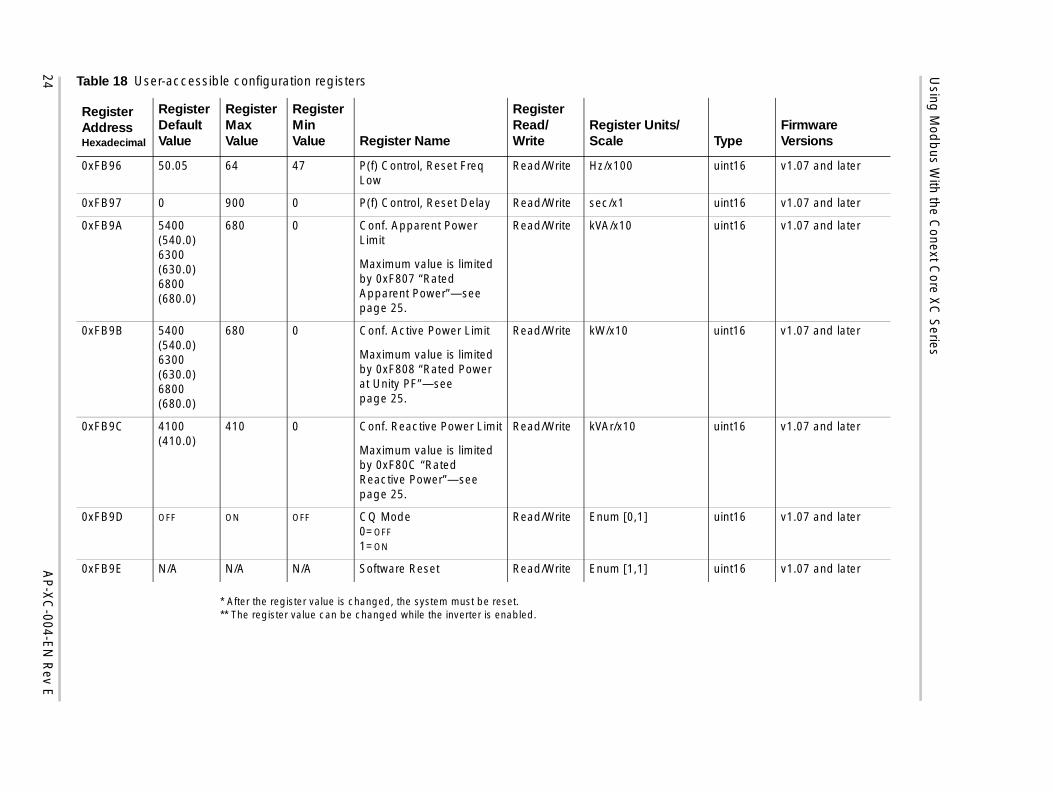
* After the register value is changed, the system must be reset.** The register value can be changed while the inverter is enabled.
0xFB96 50.05 64 47 P(f) Control, Reset Freq Low
Read/Write Hz/x100 uint16 v1.07 and later
0xFB97 0 900 0 P(f) Control, Reset Delay Read/Write sec/x1 uint16 v1.07 and later
0xFB9A 5400 (540.0)6300 (630.0)6800 (680.0)
680 0 Conf. Apparent Power Limit
Maximum value is limited by 0xF807 “Rated Apparent Power”—see page 25.
Read/Write kVA/x10 uint16 v1.07 and later
0xFB9B 5400 (540.0)6300 (630.0)6800 (680.0)
680 0 Conf. Active Power Limit
Maximum value is limited by 0xF808 “Rated Power at Unity PF”—see page 25.
Read/Write kW/x10 uint16 v1.07 and later
0xFB9C 4100 (410.0)
410 0 Conf. Reactive Power Limit
Maximum value is limited by 0xF80C “Rated Reactive Power”—see page 25.
Read/Write kVAr/x10 uint16 v1.07 and later
0xFB9D OFF ON OFF CQ Mode0=OFF
1=ON
Read/Write Enum [0,1] uint16 v1.07 and later
0xFB9E N/A N/A N/A Software Reset Read/Write Enum [1,1] uint16 v1.07 and later
Table 18 User-accessible configuration registers
Register Address Hexadecimal
Register Default Value
Register Max Value
Register Min Value Register Name
Register Read/Write
Register Units/Scale Type
Firmware Versions

Using Modbus With the Conext Core XC Series
AP-XC-004-EN Rev E 25
Read-Only Configuration Registers
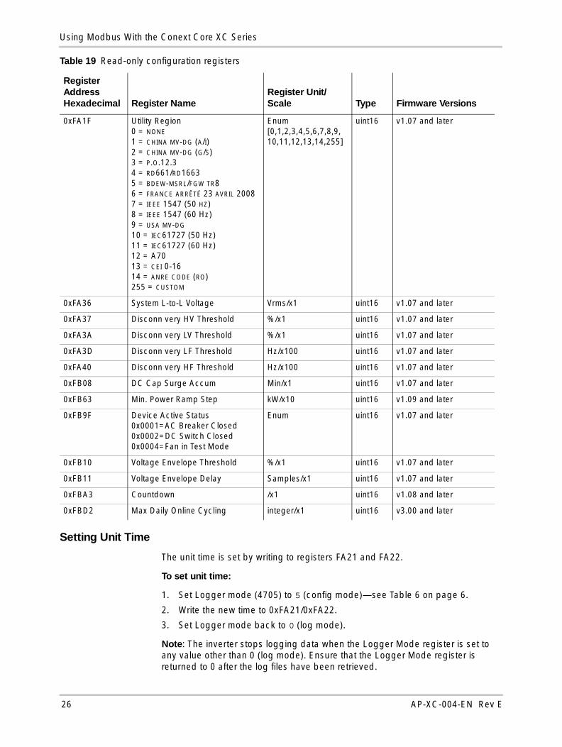
The read-only configuration registers are listed in Table 19. These registers are not accessible to users.
Table 19 Read-only configuration registers
Register Address Hexadecimal Register Name
Register Unit/Scale Type Firmware Versions
0x4009 Day Log Rate Min/x1 uint16 v1.07 and later
0x400A First Daytime Hour Hours/x1 uint16 v1.07 and later
0x400B Night Log Rate Min/x1 uint16 v1.07 and later
0x400C First Nighttime Hour Hours/x1 uint16 v1.07 and later
0x405C Grid Voltage 12 Gain Calibration x1000 uint16 v3.00 and later
0x405D Grid Voltage 23 Gain Calibration x1000 uint16 v3.00 and later
0x405E Grid Voltage 31 Gain Calibration x1000 uint16 v3.00 and later
0x405F Grid Voltage 12 Offset Calibration V/x10 sint16 v3.00 and later
0x4060 Grid Voltage 23 Offset Calibration V/x10 sint16 v3.00 and later
0x4061 Grid Voltage 31 Offset Calibration V/x10 sint16 v3.00 and later
0x4062 Gain kVAr Inductive (V2/kVAr*Hz)/x10 uint16 v3.00 and later
0x4063 Gain kVAr Capacitive (V2/kVAr*Hz)/x10 uint16 v3.00 and later
0xF801 Rated Input (PV) Current A/x1 uint16 v1.07 and later
0xF802 Maximum Input (PV) Voltage VDC/x1 uint16 v1.07 and later
0xF805 Max PV OC Voltage VDC/x1 uint16 v1.07 and later
0xF806 Max STC PV-SC Current ADC/x1 uint16 v1.07 and later
0xF807 Rated Apparent Power kVA/x10 uint16 v1.07 and later
0xF808 Rated Power at Unity PF kW/x10 sint16 v1.07 and later
0xF809 Min Input (PV) Voltage VDC/x1 uint16 v1.07 and later
0xF80A Nominal L-to-L Voltage Vrms/x1 uint16 v1.07 and later
0xF80B Nominal Line Current Arms/x1 uint16 v1.07 and later
0xF80C Rated Reactive Power kVAr/x10 sint16 v1.07 and later
0xFA0B Disconn HV Threshold %/x1 uint16 v1.07 and later
0xFA0C Disconn LV Threshold %/x1 uint16 v1.07 and later
0xFA0F Disconn HF Threshold Hz/x100 uint16 v1.07 and later
0xFA10 Disconn LF Threshold Hz/x100 uint16 v1.07 and later
0xFA1A Active Anti-Islanding Function0 = OFF
1 = ON
Enum [0,1] uint16 v1.07 and later
Using Modbus With the Conext Core XC Series
26 AP-XC-004-EN Rev E
Setting Unit Time
The unit time is set by writing to registers FA21 and FA22.
To set unit time:
1. Set Logger mode (4705) to 5 (config mode)—see Table 6 on page 6.
2. Write the new time to 0xFA21/0xFA22.
3. Set Logger mode back to 0 (log mode).
Note: The inverter stops logging data when the Logger Mode register is set to any value other than 0 (log mode). Ensure that the Logger Mode register is returned to 0 after the log files have been retrieved.
0xFA1F Utility Region0 = NONE
1 = CHINA MV-DG (A/I)2 = CHINA MV-DG (G/S)3 = P.O.12.34 = RD661/RD16635 = BDEW-MSRL/FGW TR86 = FRANCE ARRÊTÉ 23 AVRIL 2008 7 = IEEE 1547 (50 HZ)8 = IEEE 1547 (60 Hz)9 = USA MV-DG
10 = IEC61727 (50 Hz)11 = IEC61727 (60 Hz)12 = A7013 = CEI 0-1614 = ANRE CODE (RO)255 = CUSTOM
Enum [0,1,2,3,4,5,6,7,8,9,10,11,12,13,14,255]
uint16 v1.07 and later
0xFA36 System L-to-L Voltage Vrms/x1 uint16 v1.07 and later
0xFA37 Disconn very HV Threshold %/x1 uint16 v1.07 and later
0xFA3A Disconn very LV Threshold %/x1 uint16 v1.07 and later
0xFA3D Disconn very LF Threshold Hz/x100 uint16 v1.07 and later
0xFA40 Disconn very HF Threshold Hz/x100 uint16 v1.07 and later
0xFB08 DC Cap Surge Accum Min/x1 uint16 v1.07 and later
0xFB63 Min. Power Ramp Step kW/x10 uint16 v1.09 and later
0xFB9F Device Active Status0x0001=AC Breaker Closed0x0002=DC Switch Closed0x0004=Fan in Test Mode
Enum uint16 v1.07 and later
0xFB10 Voltage Envelope Threshold %/x1 uint16 v1.07 and later
0xFB11 Voltage Envelope Delay Samples/x1 uint16 v1.07 and later
0xFBA3 Countdown /x1 uint16 v1.08 and later
0xFBD2 Max Daily Online Cycling integer/x1 uint16 v3.00 and later
Table 19 Read-only configuration registers
Register Address Hexadecimal Register Name
Register Unit/Scale Type Firmware Versions

Using Modbus With the Conext Core XC Series
AP-XC-004-EN Rev E 27
Vigilohm IM400 Device Modbus MapThe Vigilohm IM400 insulation monitoring device is used only in ungrounded (floating) systems and is configured as a Modbus slave with its own Modbus address. The RS-485 Modbus interface uses the communication parameters listed in Table 20.
All Conext Core XC Series devices must be configured to use the same communication parameters. To configure the communication parameters, from the home screen of the IM400 device, select Menu > Settings > Modbus.
The registers listed in Table 21 allow you to monitor the status of the IM400 device. For complete details about the Modbus map for this device, see the Vigilohm IM400 Insulation Monitoring Device User Manual.
Table 20 IM400 Device RS-485 communication parameters
Parameter Default Value Other Values
Address 1 1...247
Auto Config OFF ON/OFF
Baud rate 19200 480096001920038400
Parity Even NoneOddEven
Table 21 IM400 read-only registers
Register Address Hexadecimal
Register Name Description Type
0x006D Product status 0x00 Normal operation0x01 Self-test0x02 Insulation fault0x03 Disconnected injection detected0x04 Over-limit capacitance0x05 inoperative product0x07 Overvoltage
uint16
0x03E8 Resistance Resistance (in Ω): When injection is inhibited, the value NaN (not a number) 0xFFC00000 is returned during a self-test
Float32
0x03EA Capacitance Capacitance (in F): When injection is inhibited, the value NaN (not a number) 0xFFC00000 is returned during a self-test
Float32
0x03F0 Injection status 0 = injection activated1 = injection deactivated
uint16

Using Modbus With the Conext Core XC Series
28 AP-XC-004-EN Rev E
Copyright © 2014 Schneider Electric. All Rights Reserved.
All trademarks are owned by Schneider Electric Industries SAS or its affiliated companies.
Exclusion for DocumentationUNLESS SPECIFICALLY AGREED TO IN WRITING, SELLER
(A) MAKES NO WARRANTY AS TO THE ACCURACY, SUFFICIENCY OR SUITABILITY OF ANY TECHNICAL OR OTHER INFORMATION PROVIDED IN ITS MANUALS OR OTHER DOCUMENTATION; (B)ASSUMES NO RESPONSIBILITY OR LIABILITY FOR LOSSES, DAMAGES, COSTS OR EXPENSES, WHETHER SPECIAL, DIRECT, INDIRECT, CONSEQUENTIAL OR INCIDENTAL, WHICH MIGHT ARISE OUT OF THE USE OF SUCH INFORMATION. THE USE OF ANY SUCH INFORMATION WILL BE ENTIRELY AT THE USER’S RISK; AND (C)REMINDS YOU THAT IF THIS DOCUMENTATION IS IN ANY LANGUAGE OTHER THAN ENGLISH, ALTHOUGH STEPS HAVE BEEN TAKEN TO MAINTAIN THE ACCURACY OF THE TRANSLATION, THE ACCURACY CANNOT BE GUARANTEED. APPROVED CONTENT IS CONTAINED WITH THE ENGLISH LANGUAGE VERSION WHICH IS POSTED AT WWW.SESOLAR.COM.
Date: June 2014 Revision: Rev E Document Number: AP-XC-004-EN
Contact InformationFor other country details please contact your local Schneider Electric Sales Representative or visit the Schneider Electric Solar website at www.sesolar.com.
0x044C Insulation alarm status
0 = no insulation alarm1 = insulation alarm active2 = preventive insulation alarm active4 = transient insulation alarm8 = insulation alarm acknowledged
uint16
Table 21 IM400 read-only registers
Register Address Hexadecimal
Register Name Description Type