Application Note - fastcomtec.com · Charge trapping happens when the transistor is in “on”...
12
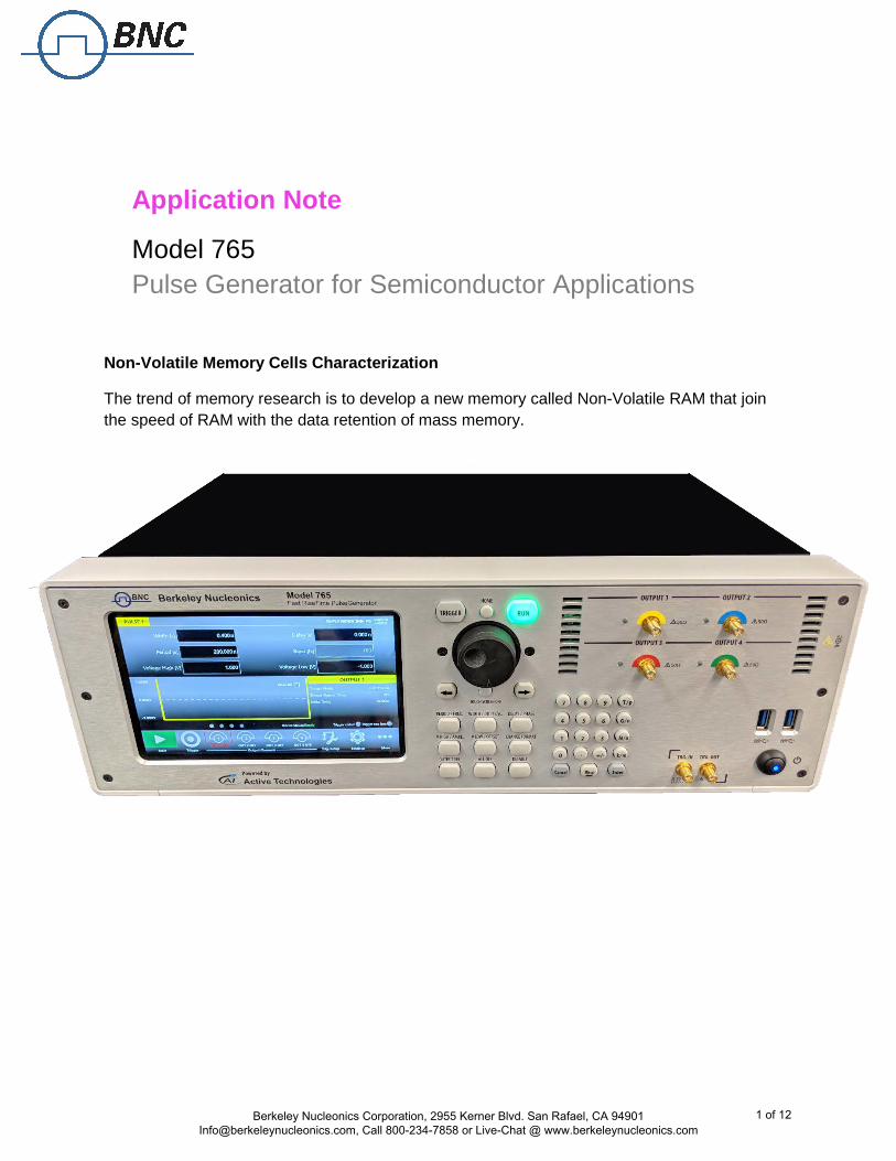
Application Note Model 765 Pulse Generator for Semiconductor Applications Non-Volatile Memory Cells Characterization The trend of memory research is to develop a new memory called Non-Volatile RAM that join the speed of RAM with the data retention of mass memory. Berkeley Nucleonics Corporation, 2955 Kerner Blvd. San Rafael, CA 94901 [email protected], Call 800-234-7858 or Live-Chat @ www.berkeleynucleonics.com 1 of 12
Transcript of Application Note - fastcomtec.com · Charge trapping happens when the transistor is in “on”...
Application Note
Model 765 Pulse Generator for Semiconductor Applications
Non-Volatile Memory Cells Characterization
The trend of memory research is to develop a new memory called Non-Volatile RAM that join the speed of RAM with the data retention of mass memory.
Berkeley Nucleonics Corporation, 2955 Kerner Blvd. San Rafael, CA 94901 [email protected], Call 800-234-7858 or Live-Chat @ www.berkeleynucleonics.com
1 of 12

There are many proposal of new cell types, for example FeRAM (Ferroelectric RAM), ReRAM (Resistive RAM), MRAM (Magnetoresistive Ram), STT-MRAM (Spin-Transfer Torque Magnetoresistive Ram) and PCM (Phase Change Memory).
Those types of memories are based on the changing of conductivity of a material using different physical principle, for example formation and destruction of a thin wire into a material stack, or the change of the material structure from amorphous to polycrystalline or the alignment of the magnetic field.
In this application note we will show how to test a STT-MRAM cell using a pulse generator.
MRAM memory cells uses Magnetic Tunnel Junctions (MTJ) that consists of two ferromagnets separated by a thin insulator. If the magnetic fields of the two ferromagnets are oriented in the same direction, electrons can tunnel from one ferromagnet to other through insulator layer. The first ferromagnet has a fixed magnetic field, while the field of the second one can be changed applying a current pulse, so inverting the magnetic field orientation changes the conductivity of the stack.
To program or erase a bit, a current pulse is applied through the stack; the assumed orientation of magnetic field depends on the current pulse direction. The efficiency of program and erase process depends on the duration and amplitude of the pulse, so during research and developing stages on this technology, it can be useful to test different combination of pulse width and amplitude: a simple way to do this is to use a pulse generator, that allow to change the width, the amplitude and the repetition rate.
Figure 1: SimpleRider PG setup to program or erase a single cell: pulse characteristics: 50 ns @ 3.3V
Berkeley Nucleonics Corporation, 2955 Kerner Blvd. San Rafael, CA 94901 [email protected], Call 800-234-7858 or Live-Chat @ www.berkeleynucleonics.com
2 of 12

Figure 2: SimpleRider PG setup to program or erase an array of cells: pulse characteristics: 100 ns @ 3.3V
Figure 3: in this example, the pulse generator supplies pulses of 50 ns @ 3.3V to simulate the program or erase of a cell.On the second channel it supplies 100 ns @ 3.3V to program or erase of a cell array.
Berkeley Nucleonics Corporation, 2955 Kerner Blvd. San Rafael, CA 94901 [email protected], Call 800-234-7858 or Live-Chat @ www.berkeleynucleonics.com
3 of 12

PCM memory cell is based on amorphous to crystalline phase changing of chalcogenide material, when the material is in amorphous phase the resistance is high and when it is in crystalline phase the resistance is lower.
To program or erase a bit it is necessary to change the phase of the material: a large but low voltage pulse changes the phase from amorphous to crystalline, on the contrary a short but higher voltage pulse changes the phase from crystalline to amorphous.
As you can see in the image the control of amplitude and width of pulses is fundamental, the Model 765 pulse generators powered by Active Technologies offer a time resolution of 10 ps and a vertical resolution of 10 mV.
Newer technologies applied on the Non-Volatile RAM require faster pulses every day: The Model 765 with transition time under 70 ps and an amplitude up to 5 Vpp is the perfect choice for those kinds of requirements.
Berkeley Nucleonics Corporation, 2955 Kerner Blvd. San Rafael, CA 94901 [email protected], Call 800-234-7858 or Live-Chat @ www.berkeleynucleonics.com
4 of 12
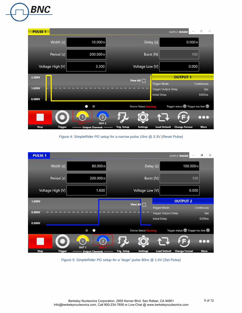
Figure 4: SimpleRider PG setup for a narrow pulse 10ns @ 3.3V (Reset Pulse)
Figure 5: SimpleRider PG setup for a “large” pulse 80ns @ 1.6V (Set Pulse)
Berkeley Nucleonics Corporation, 2955 Kerner Blvd. San Rafael, CA 94901 [email protected], Call 800-234-7858 or Live-Chat @ www.berkeleynucleonics.com
5 of 12

Figure 6: in this example, the pulse generatore supplies pulses of 10 ns @ 3.3V and 80 n @ 1.6V to simulate the erase and the program of a cell.
MOSFET Test
Developing modern MOSFET transistor, the challenge is to use high κ material for the dielectric in MOS capacitor, this give the advantage of reduce the leakage current through the isolator but at same time, it causes some problem due to charge trapping, like voltage threshold instability, carrier channel mobility degradation and finally a reduction of reliability.
Charge trapping happens when the transistor is in “on” state and a bit of channel charge are accumulated into isolation layer creating a built-in potential that changes the threshold.
The charge trapping phenomena depends on various physic parameters of gate stack such as the thickness, the type of dielectric and the technology process, but also depend on gate voltage and pulse duty cycle.
It is clear that is very important to understand the charge trapping mechanism to improve this technology.
Berkeley Nucleonics Corporation, 2955 Kerner Blvd. San Rafael, CA 94901 [email protected], Call 800-234-7858 or Live-Chat @ www.berkeleynucleonics.com
6 of 12

The order of magnitude of this phenomenon varies from under 1 µs to dozens of milliseconds then the DC measure are unreliable, therefore different type of pulsed I-V measurements are used.
All types of Id Vg measurements are obtained biasing the drain terminal and supplying pulse into the gate terminal, depending on the type of pulse it is possible to divide the measurements into 3 main categories:
• DC Id Vg curves: gate signal is a DC level, repeating the measurement for many bias point, the curve is achieved. In this way, the results depend on the charge trapping effects due to the biasing, and this measurement isn’t reliable for devices developed for switch at high rate.
• Short Pulse Id Vg curves: Supplying pulses with fast edges and a width in the order of nanoseconds, it is possible to analyze the response of intrinsic device, because the charge doesn’t have time to accumulate into dielectric layer. Finally, repeating the measurement for different bias points is possible to obtain the curve. This measure doesn’t give information about the charge trapping phenomenon.
• Slow Pulse Id Vg curves: This technique consists into supply only a long pulse (in the order of microseconds) with ramped edges. In this way, if the ramp is enough fast the result is directly the Id Vg curve of the device because the charge doesn’t have the time to accumulate in the MOS stack. The long pulse is required to measure the drain current degradation over the time and then observe the trapping charge effect, then if the goal is to study the charge trapping effect at a defined bias point, the slew rate of the edges doesn’t matter but it is only important that the rising edge is very fast. If the edges are enough fast, the obtained results are directly comparable to both DC and Short Pulse curves in that bias point because immediately after the leading edge of the gate voltage the drain current is comparable to that obtained from pulsed measurements, then the drain current start to decrease over the time until it arrives at the value measured through DC measurements. The Slow Pulse technique can also be used to predict the life time of devices developed for switching by studying the increment of charge trapping effects before and after switching stress.
Berkeley Nucleonics Corporation, 2955 Kerner Blvd. San Rafael, CA 94901 [email protected], Call 800-234-7858 or Live-Chat @ www.berkeleynucleonics.com
7 of 12

Figure 1: Principle scheme of a set-up for the Id-Vg measurement.
Figure 7: Example of comparison among the different measurement solutions.
The Model 765 pulse generator supply fast edges under 70 ps, an amplitude up to 5 Vpp, a baseline offset of +-2.5 V and a pulse width from 300 ps up to 1 s, so it may be the ideal instrument to generate the pulses for Short and Slow Pulse tests.
Berkeley Nucleonics Corporation, 2955 Kerner Blvd. San Rafael, CA 94901 [email protected], Call 800-234-7858 or Live-Chat @ www.berkeleynucleonics.com
8 of 12

Figure 8: Screen UI “short pulse” baseline -1V, max 2V2 (amplitude 3,2V) duration 30 ns single mode
Figure 9: Oscilloscope screenshot of gate pulse for short pulse MOSFET characterization
Berkeley Nucleonics Corporation, 2955 Kerner Blvd. San Rafael, CA 94901 [email protected], Call 800-234-7858 or Live-Chat @ www.berkeleynucleonics.com
9 of 12

Figure 10: Screen UI “slow pulse” baseline -1V, max 2V2 (amplitude 3,2V) duration 60 us single mode
Berkeley Nucleonics Corporation, 2955 Kerner Blvd. San Rafael, CA 94901 [email protected], Call 800-234-7858 or Live-Chat @ www.berkeleynucleonics.com
10 of 12

Figure 11: Oscilloscope screenshot of gate pulse for spct MOSFET characterization
Berkeley Nucleonics Corporation, 2955 Kerner Blvd. San Rafael, CA 94901 [email protected], Call 800-234-7858 or Live-Chat @ www.berkeleynucleonics.com
11 of 12
About Active Technologies Active Technologies is an Italian company expert in semiconductor test equipment and electronic instrumentation design.
About Berkeley Nucleonics Corporation Berkeley Nucleonics Corporation (BNC) is a leading manufacturer of precision electronic instrumentation for test, measurement, and nuclear research. Our corporate headquarters are in San Rafael, California, with additional manufacturing facilities and sales offices located throughout the United States.
The Pulse Rider Series offers premium signal integrity with the easiest to use touch screen display interface (SimpleRider™). The Generation of pulses requires only a few screen touches. Its innovative hardware architecture provides the possibility to generate multiple pulse sequences, such as double, triple or quad pulses, with fully independent timing parameters.
Berkeley Nucleonics Corporation, 2955 Kerner Blvd. San Rafael, CA 94901 [email protected], Call 800-234-7858 or Live-Chat @ www.berkeleynucleonics.com
12 of 12