Application Note: ATA6824 and ATmega88IAR EWAVR 4.20A 1 180 bytes 335 bytes All routines are...
14
Atmel ATA6824 and Atmel ATmega88: DC Motor Control in High Temperature Environment 1. Introduction The purpose of this document is to explain Atmel ® ’s High Temperature H-bridge Motor Control System. The demand for driver solutions in “under-the-hood” environments is rapidly increasing, and in particular, the use of applications such as turbo chargers, EGR, or AGR calls for new solutions. Figure 1-1. Atmel ATA6824 and Atmel ATmega88 Atmel ATA6824 and Atmel ATmega88 Application Note 9102B–AUTO–03/11
Transcript of Application Note: ATA6824 and ATmega88IAR EWAVR 4.20A 1 180 bytes 335 bytes All routines are...

Atmel ATA6824 and Atmel ATmega88:DC Motor Control in High Temperature
Environment
1. IntroductionThe purpose of this document is to explain Atmel®’s High Temperature H-bridge MotorControl System. The demand for driver solutions in “under-the-hood” environments israpidly increasing, and in particular, the use of applications such as turbo chargers,EGR, or AGR calls for new solutions.
Figure 1-1. Atmel ATA6824 and Atmel ATmega88
Atmel ATA6824 and Atmel ATmega88
Application Note
9102B–AUTO–03/11

29102B–AUTO–03/11
Atmel ATA6824/ATmega88
2. H-bridge Motor Control System
Figure 2-1. Fully Integrated H-bridge Motor Control Application
The system consists of two integrated circuits: the Atmel® microcontroller ATmega88 and theAtmel H-bridge DC Motor Driver ATA6824.
The Atmel ATA6824 features gate drivers to drive H-bridge FETs, voltage regulator, watch-dog, and serial IO interface. An integrated charge pump controls the NMOS FETs for low-sideand high-side switches. In addition, the charge pump voltage is capable of providing alow-drop inverse voltage protection. Therefore, only a NMOS FET in the source drain directionis necessary.
The Atmel ATA6824 switches the outputs off in the event of short circuits, voltage failures, andovertemperature. Temperature prewarning and charge pump failures are also indicated. Theapplication circuit includes a current shunt, which can react at different current levels. The cur-rent signal is prepared for the microcontroller by an amplifier.
The Atmel ATmega88 generates the PWM speed signal to run various movement profiles asrequired for the load.
SIO WD Timer
CC Timer
Gate Driver Low Side 2
Gate Driver Low Side 1
Gate Driver High Side 1
Gate Driver High Side 2
CP13V
Regulator
3.3V/5V VCC Regulator
Supervisor: Short Circuit Open Load
Over Temperature Under Voltage
Logic Control
ATA6824PCINT
Interrupt Pins
PWM Timer
I/Os
UART Input
Capture
ADC + Analog
Comparator
AVR ATmega88 VCC
DG1
DG2DG3
PWM
DIR
WD
/RESET
RX
TX
SIO
SIO RWD CC GNDPGND
L2
L1
S1
H1
S2
H2
VBAT
3.3V/5V VCC Regulator
VMODE VINT VG CPLO CPHI VRES PBAT
VBAT
+-
M

39102B–AUTO–03/11
Atmel ATA6824/ATmega88
2.1 Cooling Area DesignThe Atmel® driver IC ATA6824 is housed in a QFN package. QFN packages are particularlysuitable for power applications because of the exposed die pad. To make use of this advan-tage, the heat slug must be completely soldered to the PCB.
To reduce thermal resistance, vias etched down to the soldering layer are required. An ade-quate ground plane must be placed on the soldering layer to eliminate the thermal energy.
A via diameter of 0.3mm to 0.4mm with a spacing of 1mm to 1.5mm has proven to be mostsuitable. Care should be taken of the copper area's planarity to avoid, in particular, any solderbumps arising at the thermal vias.
3. High Ambient TemperatureThe application is designed for high temperature environments. The Atmel ATmega88 and theAtmel driver ATA6824 are qualified up to an ambient temperature of 150°C. Under thermaloverload conditions, the Atmel ATA6824 switches off. If the temperature exceeds the prewarn-ing threshold, the microcontroller can reduce the output power.
Capacitance material on X8R quality is necessary to ensure high ambient temperatures.
Mounted connectors, a switch, and a potentiometer on the board, enable prototyping; how-ever, these components are not qualified for use under high temperatures. The board can beintegrated into high-temperature environments using wires.
4. The Application BoardThe application board is run-capable when connected to nominal 12V at the battery connector(see Figure 4-1 on page 4). The board can be connected to the automotive environment overan SIO bus.
A mounted switch (DIR) for run/stop, clockwise, and counterclockwise movement and a poten-tiometer (SPEED) for variable speed (PWM) input are available on the application board toenable stand-alone prototyping.
An optional feedback loop from the DC motor to the Atmel ATmega88 can be establishedusing Hall sensor(s). The two Hall inputs can be linked to the connector HALL as well as the5V supply for the Hall sensors. There is also an on-board shunt current sensor to detectover-currents (using Atmel ATmega88’s analog comparator) and to measure motor current.
4.1 On Board FeaturesThe application board provides the following features:
• Atmel ATmega88 QFN32
– MCU
• Atmel ATA6824 QFN
– 5V/3.3V voltage regulator (fixed on-board to 5V)
– Low drop voltage protection management
– H-bridge driver with diagnostics
– Serial link transceiver to connect board to external environment
– Watchdog

49102B–AUTO–03/11
Atmel ATA6824/ATmega88
• On-Off-On switch
– Stand-alone commands interface: Run/stop, clockwise, and counterclockwise
• Potentiometer
– Standalone speed variation command (PWM ratio)
• System clock
– MCU internal RC oscillator
• Power H-bridge (4 power FET)
• Human interface
– Diagnostics signaling/latching through LED and unlatching through push button
• Connectors
– Power supply (battery voltage) and SIO
– DC motor connector
– Hall sensor inputs and supply (2 filtered inputs and 5V regulated supply voltage)
– SP/debugWire connector, for on-chip in-situ programming (ISP) and for on-chip debugging using JTAG ICE supported by AVR Studio® interface(1)
• Dimensions: 45mm × 90mm
Note: 1. The Atmel ATmega88 is supported by AVR Studio, version 4.12 or higher. For up-to-date information on this and other AVR® tool products, please consult our web site. The newest version of AVR Studio, AVR tools, and user guide can be found in the AVR section of the Atmel web site, http://www.atmel.com
Figure 4-1. Application Board Top View, and Connector Usage
Motor Out 1
Motor Out 2
PGND
SIO
Vbat
CWStopCCW
Speed
1 23 45 6
JP1
ISP MK2 Header
MISOSCK
NRES
MOSI
VCC 5V
GND

59102B–AUTO–03/11
Atmel ATA6824/ATmega88
5. Software DescriptionAll code is implemented in C language. Source code can be compiled using IAR® EWAVR4.20A as well as AVR-GCC (WinAVR-20060421 with AVR Studio).
HTML documentation is included in the package. Use the High_temp_brushed_DC.html file inthe root directory to start viewing the documentation.
5.1 Motor Management• Motor stopped
– PWM ratio is set to zero
– Command switch inputs are monitored to start motor or keep it stopped.
• Motor running
– Atmel® ATA6824 DIR pin is set according to command direction. PWM ratio is refreshed constantly according to speed of the potentiometer ADC input.
– Command switch inputs are monitored to stop motor or keep it stopped.
• Degraded “mode”:
– Atmel ATA6824 detects a short circuit: H-bridge short-circuited and FET is switched off until next PWM rising edge. This default is reported to software through a diagnostic feature: an interrupt occurs on DG1 MCU input pin, which internally latches a failure. Apart from switching on the DG1 LED, no action is taken by the software in response to this event. In a customer application, this should be managed, eventually by the interrupt sub-routine, especially in case of a 100% PWM ratio where no rising edge appears at the Atmel ATA6824 PWM input to make a retry. Care should be taken in motor transient state (e.g. motor start-up). An accelerating curve is preferable from 0% to 100% PWM ratio transition, which may be mistaken for a short-circuit condition. Without management, in the worst case scenario, the motor will not start as the outputs are switched off, and short circuit will be shown on DG1 pin.
– Atmel ATA6824 detects an over-temperature warning: an interrupt occurs on the MCU. This diagnostic doesn’t need to be software latched as it remains high until the temperature decreases. The application software toggles an LED.
– Atmel ATA6824 detects an under-voltage, an over-voltage, or a charge pump failure. Then, an interrupt occurs on DG2 MCU input PIN. This diagnostic is latched by software and an LED is switched on.
– An overcurrent is detected by the analog comparator. An interrupt is generated. The output PWM is then disabled until the current decreases bellow the over-current limit.
5.2 Resources
Table 5-1. Code, Data, and CPU Resources (without Compiler Optimizations)
Compiler/Resources Code Size (Flash) Data Size (Ram) CPU Load
IAR EWAVR 4.20A 1 180 bytes 335 bytesAll routines are
constantly executed in main loop
AVR-GCC 1724 bytes 15 bytes

69102B–AUTO–03/11
Atmel ATA6824/ATmega88
The following MCU peripherals are used:
• Timer 0
– PWM generation through output compare 0B (OC0B pin)
• ADC channels 0, 6, and 7
– Resp. current, battery supply voltage and desired speed (potentiometer) value acquisitions.
• Pin change interrupts
– DG1, DG2 and DG3 diagnostic pins interrupts
– Optional hall sensors
• Analog comparator
– Generates over-current interrupts
• I/O
– LEDs, switch and push-button operations, watchdog trigger, motor direction command
• Additional (not managed by this stand-alone software)
– UART for SIO implementation (communication through high-voltage serial interface).
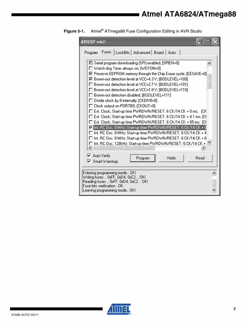
5.3 Caution about Atmel ATmega88 Start-up Time (Fuse Configuration)ATA6824 uses a windowed watchdog, which can reset the Atmel® ATmega88 using the resetpin.
• Atmel ATmega88 is configured by default (fuse configuration) with a start-up time of 65ms after a power-on reset. With tolerances, this value can increase up to 69ms.
• Atmel ATA6824 waits for a watchdog trigger within 68ms after the reset signal has been released.
Such an additional 65ms delay is unnecessary and could cause the application not to start.Atmel ATA6824 ensures an adequate VCC through its power-on delay. Atmel ATmega88default fuse configuration should be over-written with a smaller start-up time. The start-up timecan be set to 4.1ms or 0ms. The start-up settings in the fuse configuration can be changed bysetting the SUTx and CKSELx fuse bits. Further details about fuses can be found in the AtmelATmega88 datasheet and in the AVR Studio Help: AVR Tools user’s guide.
79102B–AUTO–03/11
Atmel ATA6824/ATmega88
Figure 5-1. Atmel® ATmega88 Fuse Configuration Editing in AVR Studio

89102B–AUTO–03/11
Atmel ATA6824/ATmega88
5.4 Diagrams
Figure 5-2. Flowchart for Analog Comparator (Over-current) ISR
Figure 5-3. Flowchart for Optional Hall Sensors ISR
Figure 5-4. Flowchart for Diagnostic Interrupt Pins
YN
Over-current ISR (Analog Comparator ISR)
Current Over Limit?
Latch Over Current
Report Over Current
Disable Output PWM
Clear Over-current Report
Re-enable Output PWM
Pin Change Interrupt 0 (Hall Sensor ISR)
Optional Code Can Be Put in it
Y
Pin Change Interrupt 1 (Diagnostic 1, 2 and 3 ISR
DG1 set? Latch DG1 Failure
DG2 set?
DG3 set?
Clear DG3 Warning
Latch DG2 Failure
Report DG3 Warning
Y
Y
N
N
N

99102B–AUTO–03/11
Atmel ATA6824/ATmega88
Figure 5-5. Main Loop Flowchart
5.5 Modulesvoid ADC_Init(); (void)
Sets up ADC to acquire desired speed from potentiometer.
void Timer0_start(void)
Configures timer 1 for PWM on Output compare 0 B pin.
void AN_compare_init(void)
Configures Analog comparator to detect over-currents by interrupts.
void Hall_sensors_ISR_init(void)
Sets up pin change interrupts on hall sensors inputs.
void Diag_inputs_ISR_init(void)
Sets up interrupts on Diagnostic pins.
void ADC_task(void)
Schedules ADC acquisitions: desired speed, Vbat, and Motor current. It is called in back-ground (main loop).
unsigned int adc_get_speed(void)
Returns last acquired desired speed from potentiometer.
unsigned int adc_get_current(void)
Returns last acquired motor current.
unsigned int adc_get_V_bat(void)
Returns last acquired supply voltage measurement.
void manage_time_base(void)
Main Loop (Background)
ADC Scheduler
Time Base Management
Watchdog Refresh Task
Motor Management
Diagnostic Display on LED
Initialize I/O, ATA6824 WD, ADC, Hall Sensors ISR, Diagnostic ISR, Timer0-PWM

109102B–AUTO–03/11
Atmel ATA6824/ATmega88
Manages a general purpose time base by monitoring Timer0 overflows (used by watchdogrefresh routine, LED toggling…).
void refresh_ATA6824_watchdog(void)
Refreshes ATA6824 according to hardware fixed period and software time base. It is called inbackground (main loop).
void clear_faults(void)
Clears software latched faults (from diagnostics pins) only when they have disappeared.
TIMER0_SET_OC0B_PWM (val)
This macro changes PWM ratio.
DISABLE_OCB0()
This macro disables PWM output by changing pin multiplexing back to general I/Oconfiguration.
RE_ENABLE_OCB0()
This macro enables PWM output by giving pin control to Output compare 0 B (Timer 0 PWMoutput).

119102B–AUTO–03/11
Atmel ATA6824/ATmega88
6. Application Board Full Description
Figure 6-1. BLDC Application Board Schematic
VBATSW
VBAT
PVBAT
VCC
PGND
L1
L2
NC
DIR
PWM
DG1
NC
RX
DG3
DG2
TX32
31
30
29
28
27
26
25
32
31
30
29
28
27
26
25
WD_TRIG
SIO_TXD
SIO_RXD
Mot_Dir
Diag3
Diag2
Diag1
9
10
11
12
13
14
15
16
9
10
11
12
13
14
15
16
Mot_PWM
V_Protect
VSHUNT
DG3_Fault
DG2_Fault
DG1_Fault
MOSI
MISO
SIO_TX
Mot_Dir
Mot_PWM
SIO_RXD
Diag3
Diag2
Diag3
BZX84-C5V1
PD2(INT0/PCINT18)
PD1(TXD/PCINT17)
PD0(RXD/PCINT16)
PC5(ADC5/SCL/PCINT13)
PC2(ADC2/PCINT10)
PC3(ADC3/PCINT11)
PC4(ADC4/SDA/PCINT12)
PC6(RESET/PCINT14)
H-b
ridg
e D
rive
rV
olta
ge R
egul
ator
Wat
chdo
g
U1
ATA
6824
U1
AT
meg
a88
51kΩ
R12
10kΩ
R8
470k
Ω
R3
330Ω
R5
47kΩ
R11
10kΩR1
10Ω
R18
10kΩ
R13
1 2V
MO
DE
VIN
T
RW
D
CC
RE
SE
T
WD
GN
D
SIO
3 4 5W
D_R
ES
ET
WD
_TR
IG
SIO
OR
: Net
Tie
6 7 8
1S
WIT
CH
_CC
W
Hal
l2_S
2.5V
Hal
l1_S
SW
ITC
H_C
W2 3 4 5 6 7 8
24 23 22 21 20 19 18 17
24R
ELE
AS
E_B
P
VS
HU
NT
Spe
ed_S
et
Vba
t_M
eas
SC
K
23 22 21 20 19 18 17
VR
ES
HS
ide2
Cm
d
Mot
Sid
e2
HS
ideC
md
Mot
Sid
e1
PC
1(A
DC
1/P
CIN
T9)
PC
0(A
DC
0/P
CIN
T8)
AD
C7
GN
D
AR
EF
PB
5(S
CK
/PC
INT
5)
AV
CC
AD
C6
PD
3(IN
T1/
OC
2B/P
CIN
T19
)
PD
4(T
0/X
CK
/PC
INT
20)
GN
D
VC
C
GN
D
PB
7(T
OS
C2/
XTA
L2/P
CIN
T7)
PB
6(T
OS
C1/
XTA
L1/P
CIN
T6)
VC
C
PD5(T1/OC0B/PCINT21)
PD6(AIN0/OC0A/PCINT22)
PD7(AIN1/PCINT23)
PB0(ICP1/CLKO/PCINT0)
PB1(OC1A/PCINT1)
PB2(OC1B/SS/PCINT2)
PB4(MISO/PCINT4)
PB3(MOSI/OC2A1/PCINT3)
GN
D
DIR
GN
D
GN
D
AG
ND
AG
ND
SW
ITC
H_C
CW
ON
/OF
F/O
N S
witc
hR
ight
Ang
le
SW
ITC
H_C
W
RE
LEA
SE
BP
RE
LEA
SE
SIO
3
PG
ND
12
1 21234
C1
C3
100n
F50
V
C5
2.2µ
F
D1
GF
1GC
2
C17
220n
F
C19
330p
F
Pba
t
Pba
t
Pba
t
L1 6µH
10µF
50V
C6
100µ
F/ 5
0V
C27
100n
F
C18
220n
F
C10
C8
100n
F
C33
100n
F
C21
HS
ide1
Cm
d
Mot
_Sid
e1
Hal
l1_S
Hal
l2_S
Mot
_Sid
e1
Mot
_Sid
e2M
ot_S
ide2
Mot
_Sid
e1M
ot_S
ide2
HS
ide2
Cm
d
10nF
C22
10nF
C23
35 2
1
4.7n
F
C4
D2
100n
F
100n
F
C13
470n
F
C16
1nF
C15
1nF
C20
100n
F
C14
D3
BA
S16
Q2
BC
817-
4047
0nF
100n
F50
V
PG
ND
PG
ND
PG
ND
AG
ND
AG
ND
AG
ND
DG
2
LED
CM
S R
ed
AG
ND
AG
ND
AG
ND
GN
D
GN
D
PG
ND
PG
ND
PG
ND
GN
D
TP
1
Q1
SU
D50
N04
Q3
SU
D50
N04
Q4
SU
D50
N04
VR
ES
VC
C/ 5
V
VC
C/ 5
V
VC
C/ 5
VP
bat
PG
ND
GN
D
GN
D
GN
D
GN
D
LSid
e2C
md
LSid
e1C
md
+
OR
: Net
Tie
VC
C/ 5
V
PG
ND
Vba
tV
bat
Bat
and
SIO
MO
SI
MIS
OS
CK
NR
ES
JP1
2
GN
D
64
1 53
ISP
MK
2 H
eade
r
GN
D
SP
EE
D
GN
D
VC
C/ 5
V
HA
LL
MP
T4
VG
CP
LO
CP
HI
VR
ES
H2
S2
H1
S1
10kΩ
100k
ΩS
peed
Set
PW
RLE
D C
MS
Gre
en
R9
VC
C/ 5
VV
CC
/ 5V
VC
C/ 5
V
VC
C/ 5
V
VC
C/ 5
VU
3O
PA33
3
VS
HU
NT
DG
2_Fa
ult
Vba
t
Sup
ply
Vol
tage
Mea
sure
men
t
H-B
ridg
e D
iagn
ostic
Dis
play
Low
Dro
p R
ever
se V
olta
ge P
rote
ctio
n
VB
at_M
eas
WD
_RE
SE
T
WD
NR
ES
Pba
t
MO
T_C
W
MO
T_C
W
Mot
or R
otat
ing
Dire
ctio
n
Opt
iona
l Hal
l Sen
sors
Ove
r C
urre
nt C
ompa
re
LED
CM
S Y
ello
w
LED
CM
S B
lue
V+
+ -V
-
R2
120k
Ω
R21
470k
ΩR
2047
0kΩ
R16
4.7Ω
C24
4.7n
F
R17
4.7Ω
R4
10kΩ
R6
10kΩ
AG
ND
AG
ND
10Ω
R19
1kΩ
R15
10Ω
R22
C29
LSid
e1C
md
LSid
e2C
md
10nF
C28
10nF
C25
4.7n
F
Q5
SU
D50
N04
Q6
SU
D50
N04
C32
100n
F
C30
100p
F
R25
470k
ΩR
2647
0kΩ
R29
10kΩ
R7
47kΩ
R10
47kΩ
R32
10kΩ
R27
4.7Ω
R33
249k
Ω
R14
120k
Ω
R35
120k
Ω
R30
SH
UN
T 5
mΩ
C26
4.7n
F
C31 1n
F
R28
4.7Ω
2.2k
ΩR
31
330Ω
R36
249k
Ω
R24
DG
1
LED
CM
S R
ed
DG
1_Fa
ult
Shu
nt o
f 5m
Ω --
> G
ain
= 2
5D
efec
t > 2
0A
VS
hunt
= 1
00m
V
VA
mpl
= 2
.5V
330Ω
R34
DG
3
LED
CM
S R
ed
DG
3_Fa
ult
330Ω
R37
10Ω
R23
4
VC
C/ 5
V
VC
C/ 5
V
VC
C/ 5
V
MO
T

129102B–AUTO–03/11
Atmel ATA6824/ATmega88
Figure 6-2. BLDC Application Board Top View and Component Placement
Figure 6-3. BLDC Application Board Bottom View

Atmel Corporation2325 Orchard ParkwaySan Jose, CA 95131USATel: (+1)(408) 441-0311Fax: (+1)(408) 487-2600
Atmel Asia LimitedUnit 01-5 & 16, 19/FBEA Tower, Millennium City 5418 Kwun Tong RoadKwun Tong, KowloonHONG KONGTel: (+852) 2245-6100Fax: (+852) 2722-1369
Atmel Munich GmbHBusiness CampusParkring 4D-85748 Garching b. MunichGERMANYTel: (+49) 89-31970-0Fax: (+49) 89-3194621
Atmel Japan9F, Tonetsu Shinkawa Bldg.1-24-8 ShinkawaChuo-ku, Tokyo 104-0033JAPANTel: (+81) (3) 3523-3551Fax: (+81) (3) 3523-7581
© 2011 Atmel Corporation. All rights reserved. / Rev.: 9102B–AUTO–03/11
Atmel®, Atmel logo and combinations thereof, AVR®, AVR® logo, AVR Studio® and others are registered trademarks or trademarks of Atmel Cor-poration or its subsidiaries. Other terms and product names may be trademarks of others.
Disclaimer: The information in this document is provided in connection with Atmel products. No license, express or implied, by estoppel or otherwise, to any intellec-tual property right is granted by this document or in connection with the sale of Atmel products. EXCEPT AS SET FORTH IN THE ATMEL TERMS AND CONDITIONSOF SALES LOCATED ON THE ATMEL WEBSITE, ATMEL ASSUMES NO LIABILITY WHATSOEVER AND DISCLAIMS ANY EXPRESS, IMPLIED OR STATUTORYWARRANTY RELATING TO ITS PRODUCTS INCLUDING, BUT NOT LIMITED TO, THE IMPLIED WARRANTY OF MERCHANTABILITY, FITNESS FOR A PARTICU-LAR PURPOSE, OR NON-INFRINGEMENT. IN NO EVENT SHALL ATMEL BE LIABLE FOR ANY DIRECT, INDIRECT, CONSEQUENTIAL, PUNITIVE, SPECIAL ORINCIDENTAL DAMAGES (INCLUDING, WITHOUT LIMITATION, DAMAGES FOR LOSS AND PROFITS, BUSINESS INTERRUPTION, OR LOSS OF INFORMATION)ARISING OUT OF THE USE OR INABILITY TO USE THIS DOCUMENT, EVEN IF ATMEL HAS BEEN ADVISED OF THE POSSIBILITY OF SUCH DAMAGES. Atmelmakes no representations or warranties with respect to the accuracy or completeness of the contents of this document and reserves the right to make changes tospecifications and products descriptions at any time without notice. Atmel does not make any commitment to update the information contained herein. Unless specif-ically provided otherwise, Atmel products are not suitable for, and shall not be used in, automotive applications. Atmel products are not intended, authorized, or war-ranted for use as components in applications intended to support or sustain life.

Mouser Electronics
Authorized Distributor
Click to View Pricing, Inventory, Delivery & Lifecycle Information: Atmel:
ATA6824-DK