Application Note AN-1162 - Széchenyi István Egyetemszeliz/Teljesitmenyelektronika/LTSpice/Buck...
36
www.irf.com 1 AN-1162 Application Note AN-1162 Compensator Design Procedure for Buck Converter with Voltage-Mode Error-Amplifier By: Amir M. Rahimi, Parviz Parto, and Peyman Asadi Table of Contents Page 1. Introduction to Synchronous Buck Converter ................................... 2 2. Loop Gain of the System.................................................................. 5 3. Step by Step Compensator Design Procedure................................. 6 4. Type II Compensator Design............................................................ 7 4.1 Design Example of Type II Compensator ....................................... 11 5. Type III Compensator ....................................................................... 13 5.1 Type III- A Compensator ................................................................ 14 5.2 Design Example of Type III-A Compensator .................................. 16 5.3 Type III- B Compensator ................................................................ 19 5.4 Design Example of Type III-B Compensator .................................. 20 6. Conclusion ....................................................................................... 23 Appendices: Designing the Power Stage of the Synchronous Buck Converter ........ 24 Some Special Cases of Compensator Design ..................................... 28 Loop Response Measurement ............................................................. 33
-
Upload
nguyendien -
Category
Documents
-
view
219 -
download
0
Transcript of Application Note AN-1162 - Széchenyi István Egyetemszeliz/Teljesitmenyelektronika/LTSpice/Buck...
www.irf.com 1AN-1162
Application Note AN-1162
Compensator Design Procedure for Buck Converter with Voltage-Mode Error-Amplifier
By: Amir M. Rahimi, Parviz Parto, and Peyman Asadi
Table of Contents
Page 1. Introduction to Synchronous Buck Converter ...................................2 2. Loop Gain of the System..................................................................5 3. Step by Step Compensator Design Procedure.................................6 4. Type II Compensator Design............................................................7 4.1 Design Example of Type II Compensator.......................................11 5. Type III Compensator.......................................................................13 5.1 Type III- A Compensator ................................................................14 5.2 Design Example of Type III-A Compensator ..................................16 5.3 Type III- B Compensator ................................................................19 5.4 Design Example of Type III-B Compensator ..................................20 6. Conclusion .......................................................................................23 Appendices: Designing the Power Stage of the Synchronous Buck Converter ........24 Some Special Cases of Compensator Design .....................................28 Loop Response Measurement .............................................................33
www.irf.com 2AN-1162
Compensator Design Procedure for Buck Converter
with Voltage-Mode Error-Amplifier
Synchronous buck converters have received great attention in low voltage DC/DC
converter applications because they can offer high efficiency; provide more precise
output voltage and also meet the size requirement constraints. International Rectifier Inc.
has developed a series of integrated buck regulators (SupIRBuckTM) to accommodate all
the above. These regulators combine IR’s latest MOSFET technology with high
performance process technology for IC controller. These regulators use a PWM voltage
mode control scheme with external loop compensation to provide good noise immunity
and maximum flexibility in selecting inductor values and capacitor types. The switching
frequency can be programmed from 250kHz to above 1.5MHz to provide the capability
of optimizing the design in terms of size and performance.
In this application note stabilizing the buck converter with voltage-mode error amplifier
is discussed. The goal is to highlight the advantage of this control scheme and illustrate
how a high performance feedback loop that allows fast load transient response and
accurate steady state output can be achieved.
1. Introduction to Synchronous Buck Converter with Voltage-Mode Error-
Amplifier
A buck converter with voltage-mode control and voltage-mode error amplifier can be
stabilized with a proportional-integral (PI) type of compensator. However, to have high
performance a more sophisticated compensation network is required, especially when
MLCC (Multi Layer Ceramic Capacitor) capacitors are used. MLCC capacitors are
widely used at the output of low voltage DC/DC converters because of their low
equivalent series resistance (ESR) and low equivalent series inductance (ESL). Low ESL,
which results in high resonance frequency, makes the MLCC capacitors desirable at high
switching frequencies. Besides, low ESL and low ESR make the output voltage switching
ripple smaller which is very desirable. On the other hand, stabilizing a DC/DC converter

www.irf.com 3AN-1162
with MLCC output capacitors requires more attention as compared to stabilizing a
converter with electrolytic output capacitors. Depending on the type/size of the
components of output filter which are used and the design parameters (switching
frequency, bandwidth, etc), different compensation networks might be required. In
addition, to achieve the desired performance, the parameters of the compensation
network must be adjusted properly. This document provides guidelines to design
appropriate compensation network in various conditions. In addition, the procedure of
compensator design has been explained with examples.
Figure 1 shows a typical synchronous buck converter with voltage-mode control and
voltage-mode error-amplifier.
Gate Drivers
RLoad
Co
ESR
LoRL
Vin+-
Output Inductor
Output Capacitor
Control FET
Sync FET
Vosc
+-
PWM Generator
-+ Vref
Error Amplifier
Compensation Network
Vout
Ve
Figure 1 - Simplified circuit diagram of a synchronous buck converter with a voltage-
mode error-amplifier
In Figure 1, LR is the inherent resistance of the output inductor and ESR is the equivalent
series resistance of the output capacitor. To make the analysis simpler, the ESL of the
output capacitors is neglected. The circuit shown in Figure 1 can be modeled with three
blocks as presented in Figure 2. The power stage (Gp(s)) includes the switches, the
drivers and the output inductor and capacitor. The model of the PWM generator is simply
oscV/1 [2], where oscV is the peak to peak amplitude of the oscillator voltage (saw-tooth)

www.irf.com 4AN-1162
listed in the datasheet. The compensator block (H(s)) represents the error-amplifier with
the compensation network.
Vref H(s)
Compensator
Ve
oscV
1
PWM Generator
d(duty cycle)
+-
GP(s)G(s)
Vout
Power Stage
k
1
Figure 2 - The block diagram model of the synchronous buck converter
The transfer function of the power stage can be simplified as follows:
inLoadoLoadoLoadoo
oLoadoutP V
R)ESRCRL(s)ESRR(sCL
)sESRC(R)s(
d
V)s(G
2
1 (1)
The ‘s’ indicates that the transfer function varies as a function of the frequency. For
simplicity the transfer functions of the PWM generator and the power stage can be
combined:
oscP V
)s(G)s(G1
(2)
Therefore, G(s) is usually referred to as the transfer function of the power stage. The
roots of the polynomial in the denominator of (1) are called the poles of the transfer
function of the power stage. Similarly the roots of the numerator of (1) are the zeros of
the transfer function of the power stage. The transfer function of the power stage is a
second order system with a double pole at the resonance frequency (of the LC filter) and
a zero produced by the ESR of the output capacitor. The resonance frequency and the
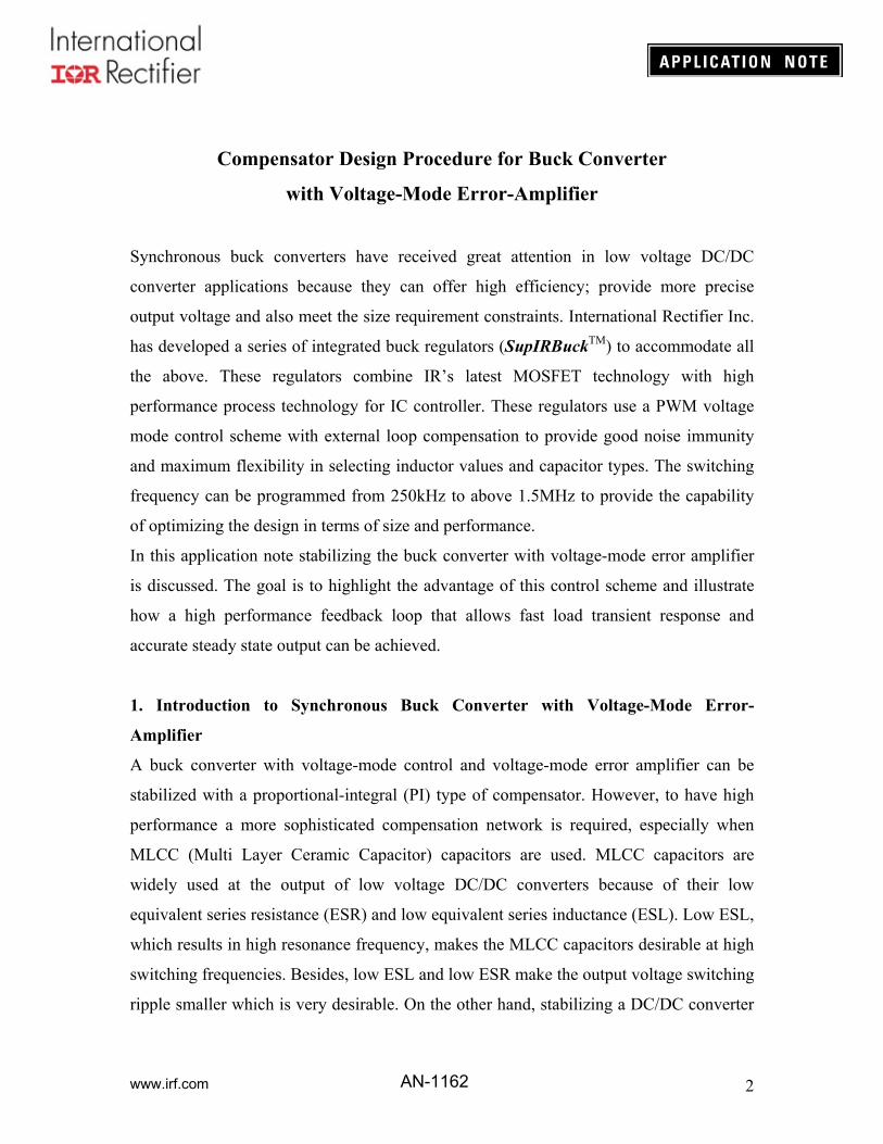
zero frequency associated with the ESR are given by (3) and (4). The approximate Bode
plot of the power stage is sketched in Figure 3. The double pole causes the gain to fall
with a slope of -40dB/dec up to the zero frequency ( ESRF ) which compensates one of the
poles. The zero frequency is a characteristic parameter of the output capacitor and is
dependant on the type of the capacitor used. This frequency can be as low as a few kHz
www.irf.com 5AN-1162
for an electrolytic capacitor to as high as a few MHz for a ceramic capacitor. More
information about designing the power stage is provided in Appendix A.
oo
LCCLπ
F
2
1 (frequency of the double poles) (3)
oESR CESRπ
F
2
1 (frequency of the zero) (4)
Phase
-40dB
-20dB
Magnitude
FESR
FLC
osc
in
VV
-180°
-90°
0
Figure 3 - The bode plot of the power stage of the buck converter
2. Loop Gain of the system
The loop gain of system is defined as the product of transfer functions along the closed
control loop. Using Figure 2, the loop gain is defined as:
)s(G)s(Hk
)s(GV
)s(Hk
)s(M Posc
111
(5)
Where k1 represents the gain of the resistor divider which is used in the feedback loop
when refout VV . For some configurations of compensation network, as the ones
discussed in the next sections, this term ( k1 ) is canceled out and does not appear in the
loop-gain equation.
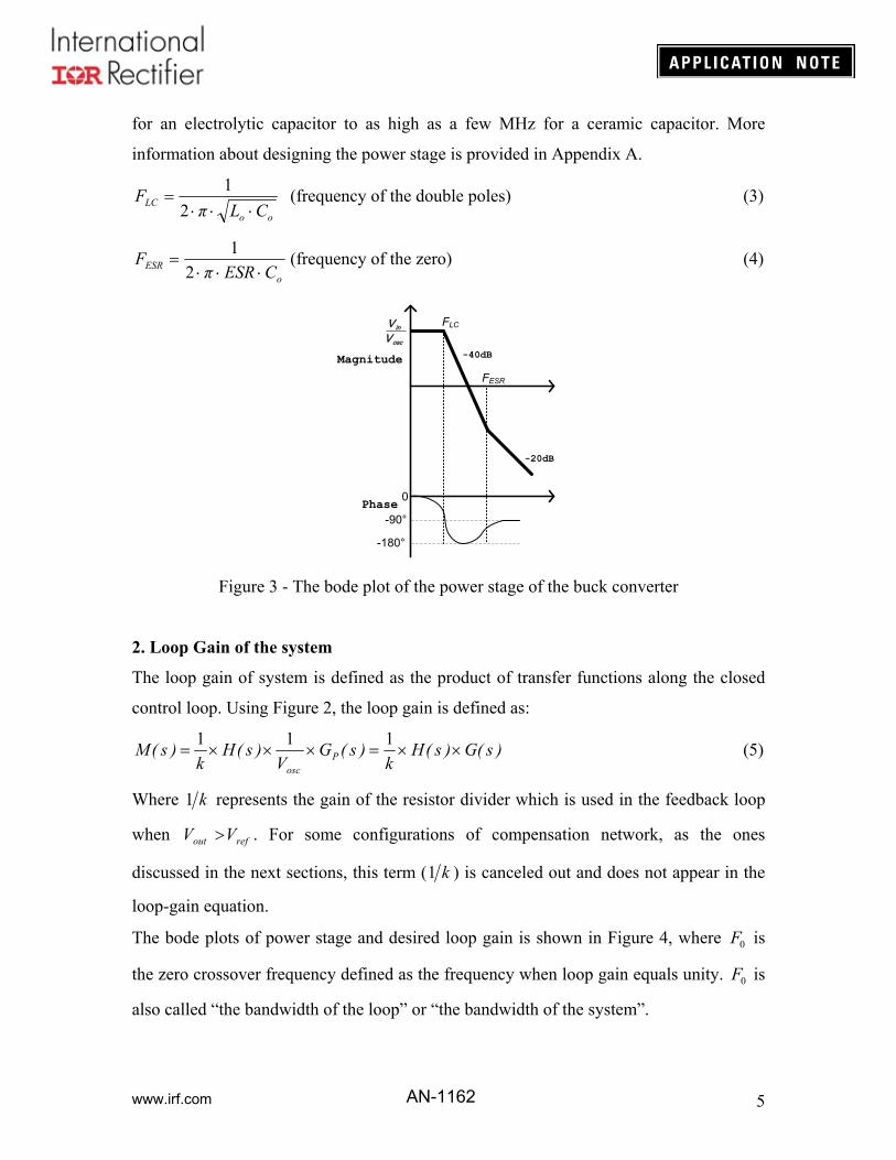
The bode plots of power stage and desired loop gain is shown in Figure 4, where 0F is
the zero crossover frequency defined as the frequency when loop gain equals unity. 0F is
also called “the bandwidth of the loop” or “the bandwidth of the system”.
www.irf.com 6AN-1162
Typically, 0F can be set to 1/10~1/5 of the switching frequency. The speed of the system
response to load transients is determined by 0F . In other words, the higher the crossover
frequency, the faster the load transient response would be. However, the crossover
frequency should be low enough to allow attenuation of switching noise. The slope of the
loop gain at 0F should be about –20dB in order to ensure a stable system. The phase
margin should be greater than 45º for overall stability.
osc
in
VV
Figure 4 - Bode plot of the power stage, desired loop gain, and loop phase
3. Step by step compensator design procedure
As mentioned in the Introduction, to have a stable closed loop buck converter with
appropriate performance, a properly designed compensator is required. The typical
procedure of compensator design is as follows:
Step 1 - Collect system parameters such as input voltage, output voltage, maximum
load/output current, switching frequency, input and output capacitance, and output
inductance.
Step 2 - Using (3) and (4) determine the power stage poles and zero
Step 3 - Determine the zero crossover frequency of the loop, 0F . Usually this frequency
is chosen equal to 1/10 to 1/5 of the switching frequency.

www.irf.com 7AN-1162
SF)/~/(F 511010 (6)
Step 4 - Determine the compensation type. The compensation type is determined by the
location of zero crossover frequency and characteristics of the output capacitor as shown
in Table 1.
Step 5 - Determine the desired location of the poles and zeros of the selected
compensator (this will be explained for each type of compensator).
Step 6 - Calculate the real parameters (resistors and capacitors) for the selected
compensator so that the desired poles/zeros are achieved. Choose the standard values for
resistors and capacitors such that they are as close to the calculated values as possible.
Table 1 - The compensation type and location of zero crossover frequency.
Compensator Type Relative location of the crossover
and power-stage frequencies Typical Output Capacitor
Type II (PI) 2/0 SESRLC FFFF Electrolytic, POS-Cap, SP-Cap
Type III-A (PID) 2/0 SESRLC FFFF POS-Cap, SP-Cap
Type III-B (PID) ESRSLC FFFF 2/0 Ceramic
4. Type II Compensator Design
Type II compensation is used for applications where the frequency of the zero caused by
output capacitor and its ESR ( ESRF ) is smaller than the closed loop bandwidth ( 0F ) as
shown below:
20 /FFFF SESRLC (7)
This condition is usually met when the output capacitor is of electrolytic type. The ESRF
(refer to (4)) for this type of capacitor is in the range of a few kHz.
The schematic of the type II compensator is depicted in Figure 5.

www.irf.com 8AN-1162
E/A+
-
Rf2
Rf1
Vref
Rc1
Vout
Cc1
Cc2
Zc
Ve
Figure 5 - Type II compensator
Assuming the gain/band-width of the error-amplifier (E/A) is very high, the transfer
function of this compensator is given by:
)sCC
CCR()CC(sR
sCR)s(
V
V)s(H
CC
CCCCC
CC
out
e
1
1
21
211211f
11
(8)
The capacitor 2CC is chosen so that 12 CC CC . Therefore:
)sCR(CsR
sCR)s(H
CCC
CC
1
1
2111f
11
(9)
The root of the numerator in (8) is the zero of compensator and the roots of the
denominator are the poles of the compensator. Therefore, the compensator has a pole at
the origin (an integrator) and another pole and one zero as given below:
111 2
1
CCZ CRπ
F
(10)
212 2
1
CCP CRπ
F
(11)
The approximate bode-plot of the power stage, the Type II compensator, and the desired
loop gain has been drawn in Figure 6.
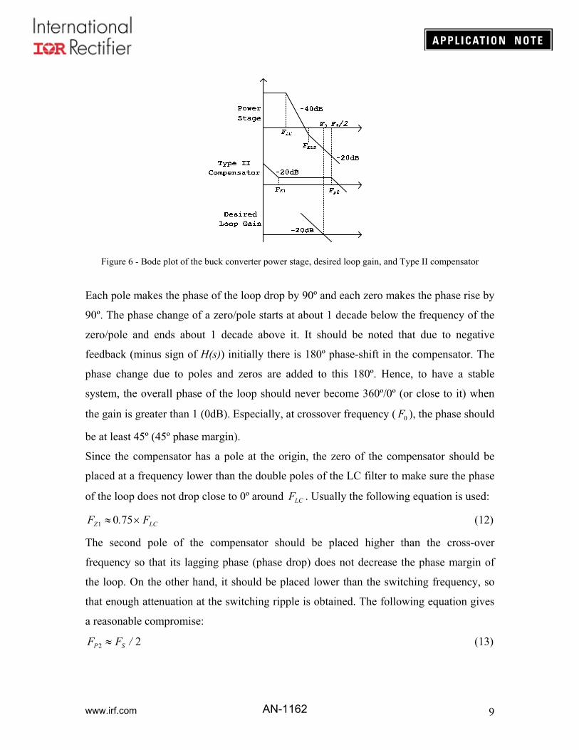
www.irf.com 9AN-1162
Figure 6 - Bode plot of the buck converter power stage, desired loop gain, and Type II compensator
Each pole makes the phase of the loop drop by 90º and each zero makes the phase rise by
90º. The phase change of a zero/pole starts at about 1 decade below the frequency of the
zero/pole and ends about 1 decade above it. It should be noted that due to negative
feedback (minus sign of H(s)) initially there is 180º phase-shift in the compensator. The
phase change due to poles and zeros are added to this 180º. Hence, to have a stable
system, the overall phase of the loop should never become 360º/0º (or close to it) when
the gain is greater than 1 (0dB). Especially, at crossover frequency ( 0F ), the phase should
be at least 45º (45º phase margin).
Since the compensator has a pole at the origin, the zero of the compensator should be
placed at a frequency lower than the double poles of the LC filter to make sure the phase
of the loop does not drop close to 0º around LCF . Usually the following equation is used:
LCZ F.F 7501 (12)
The second pole of the compensator should be placed higher than the cross-over
frequency so that its lagging phase (phase drop) does not decrease the phase margin of
the loop. On the other hand, it should be placed lower than the switching frequency, so
that enough attenuation at the switching ripple is obtained. The following equation gives
a reasonable compromise:
22 /FF SP (13)

www.irf.com 10AN-1162
After 1ZF and 2pF are selected the values of the components of the compensator can be
calculated.
There is one degree of freedom in calculating the values of the parameters of the
compensator. The procedure can be started by selecting a reasonable value for 1fR . A
value of a few kΩ should be a good starting point. Since 1fR and f2R are used to set the
output voltage (Figure 5), f2R can be calculated using the following equation:
)VV(
VRR
refout
ref
1f
2f (14)
The transfer function from the output of the error amplifier to the output voltage is:
LoadoLoadoLoadoo
oLoad
osc
in
e
out
RESRCRLsESRRsCL
sESRCR
V
Vs
V
VsG
)()(
)1()()(
2 (15)
In the above equation, oscV is the amplitude of the saw-tooth/triangular modulator signal
The amplitude of the loop-gain at crossover frequency is equal to one. Therefore,
1)()(0
FfsGsH (16)
Using the (9), (15), and (16) 1CR is calculated:
201f
1LCin
oscESRC FV
FVFRR
(17)
Since 1ZF was chosen and 1CR was calculated, 1CC can be calculated:
LCCZCC FRπ.FRπ
C
111
1 51
1
2
1 (18)
Similarly, 2CC can be calculated:
SCPCC FRπFRπ
C
121
2
1
2
1 (19)

www.irf.com 11AN-1162
4.1 Design example of Type II compensator
For this design an IR3840 regulator is used. The schematic of the design is given in
Figure 7.
Boot
Vcc
Fb
CompGnd PGnd
SW
OCSet
SS / SD
4.5 V < Vcc<5.5V
Vout
PGood
PGood
Enable
Rt
Vin =12 V
Vin
Seq
Rf1
Lo
ROCSet
3.24k
C60. 1 uF
CSS
0. 1 uF
Cin = 4 X 10 uF +330 uF
Rt23.2k
RPG
10K
R1
49.9K
R2
6.8K
IR3840
1 uF
CVcc1.8V
Co=2x470µF, 10mΩ eachRf2
1.2kΩ 1%
768Ω 1%
Cc2
530nH
Cc1
Rc1
POSCAP 7.15kΩ
4.7nF
68pF
+-
Figure 7 - Application of IR3840 with type II compensator for a 12A, 1.8V regulator
Step 1 - Collect the system information such as input and output voltage and the
switching frequency:
A(max)I
KHzF
eachmCESR
FμC
nHL
V.V
V.V
V.V
VV
o
S
o
o
o
osc
ref
out
in
12
600
10)(
4702
530
81
70
81
12
Step 2 - Calculate the poles and zero of the power stage. Using (3), the double pole of the
power stage is at:
KHz.FμnHπCLπ
Foo
LC 179405302
1
2
1

www.irf.com 12AN-1162
The zero caused by the ESR of the output capacitor can be calculated using (4):
kHz.FμmπCESRπ
Fo
ESR 833470102
1
2
1
Step 3 - Select crossover frequency to be 1/10 of the switching frequency:
KHzF 600
Step 4 - Select the type of compensator. Since 20 /FFFF SESRLC , Type II
compensator is suitable for this application.
Step 5 - Select the pole and zero of the compensator. Using (13) and (12):
kHz/kHz/FF
kHz.kHz..F.F
SP
LCZ
30026002
33517750750
2
1
Step 6 - Calculate the parameters (resistors and capacitors) of the compensator. Select
KR 2.11f . 2fR is calculated using (14):
764)7.08.1(
7.02.12f VV
VkR
Select 7682fR . Calculate 1CR using (17):
k.
)kHz.(V
kHzV.kHz.k.RC 247
1712
60818332121
Choose k.RC 1571 . Calculate 1CC using (18):
nF.kHz.k.π
CC 243351572
11
Choose nF.CC 741 . Calculate 2CC using (19):
pFkHzk.π
CC 743001572
12
Choose pFCC 682 . The experimentally measured Bode plot of the loop for this design
is shown in Figure 8. The resulting crossover frequency is about 61kHz and the phase
margin is about 54º.

www.irf.com 13AN-1162
Figure 8 - The bode plot of the loop for the example with Type II compensator
5. Type III Compensator
For a general solution for unconditional stability for any type of output capacitors, and a
wide range of ESR values, local feedback should be implemented with a type III
compensation network. Specially, when ESRFF 0 type II compensator is not useful and
type III compensator must be used. The typically type III compensation network which is
used for a voltage-mode PWM converter is shown in figure 9.
E/A+
-
OUTRf2
Rf1
Vref
Rc1
Vout
Cc1
Cc2
Zc
Cf3
Rf3
Zf
Ve
Figure 9 - Type III compensator
The transfer function of type III compensator is given by:
f
)(Z
Z
V
VsH C
out
e (20)

www.irf.com 14AN-1162
)1()](1[)(
)](1[)1()(
3f3f21
211211f
3f1f3f11
CRsCC
CCRsCCRs
RRCsCRssH
CC
CCCCC
CC
(21)
The pole which is generated by 2CC and 1CR is usually set at a much higher frequency as
compared with the frequency of the zero generated by 1CC and 1CR . This means:
12 CC CC . Therefore:
)1()1(
)](1[)1()(
3f3f2111f
3f1f3f11
CRssCRCRs
RRCssCRsH
CCC
CC
(22)
The compensator has two zeros and three poles as given below:
111 2
1
CCZ CR
F
(23)
)(2
1
3f1f3f2 RRC
FZ
(24)
01 pF (25)
3f3f2 2
1
RCFp
(26)
213 2
1
CCp CR
F
(27)
Depending upon the relative location of ESRF , type III compensator design is divided into
two categories: Type III-A and Type III-B compensators.
5.1 Type III- A Compensator
If the zero cased by the ESR is below half of the switching frequency, that is if (28) is
valid, Type III-A compensation method is used.
2/0 SESRLC FFFF (28)
Condition (28) might happen when OSCON, POS-cap or SP-Cap types of capacitors are
used at the output of the DC/DC converter. If this happens, the poles and zeros of the
compensator will be placed as follows:

www.irf.com 15AN-1162
LCZ FF 2 (29)
LCZZ FFF 75.075.0 21 (30)
ESRp FF 2 (31)
2/3 Sp FF (32)
The approximate bode-plot of the power stage for the Type III-A compensator and the
desired loop gain has been drawn in Figure 10.
Type III-ACompensator
FZ2 Fp2 Fp3=FS/2
-40dB
F0
FZ1
Desired Loop Gain
-20dB
-20dB
-20dB -20dB
PowerStage
-40dB
FESR
FLC
Figure 10 - Bode plot of the buck converter power stage, desired loop gain, and Type III-A compensator
The first zero of the compensator ( 1ZF ) compensates the phase lag of the pole which is at
the origin. The second zero ( 2ZF ) is to compensate for one of the poles of the LC filter so
that at 0F the slope of the bode plot of the loop is about -20dB/dec. The second pole of
the compensator ( 2pF ) and the zero of the ESR of the capacitor ( ESRF ) cancel each other
and the third pole ( 3pF ) is to provide more attenuation for frequencies above 2/SF .
The parameters of the compensator can be calculated as follows. First a value for 3fC is
selected (2.2nF can be a good start). Using (26) 3fR is calculated:

www.irf.com 16AN-1162
23f3f 2
1
pFCR
(33)
Using (24) 1fR is calculated:
3f23f
1f 2
1R
FCR
Z
(34)
Using (14), 2fR is calculated and 1CR is calculated using the following equation:
3f
01
2
CV
VCLFR
in
oscooC
(35)
Using (23) calculate 1CC :
111 2
1
ZCC FR
C
(36)
Using (27) calculate 2CC :
312 2
1
pCC FR
C
(37)
5.2 Design example of Type III-A compensator
For this design, as shown in Figure 11, IR3840 regulator is used.
Boot
Vcc
Fb
CompGnd PGnd
SW
OCSet
SS / SD
4.5 V < Vcc<5.5V
Vout
PGood
PGood
Enable
Rt
Vin =12 V
Vin
Seq
Rf1
Lo
ROCSet
3.24k
C60. 1 uF
CSS
0. 1 uF
Cin = 4 X 10 uF +330 uF
Rt23.2k
RPG
10K
R1
49.9K
R2
6.8K
IR3840
1 uF
CVcc1.8V
Co=2x100µF, 8mΩ eachRf2
4.64kΩ 1%
2.94kΩ 1%
Cc2
560nH
Cc1
Rc1
SP-Cap EEFSL0E101R4.22kΩ
3.9nF
120pF
Rf3402Ω
Cf3
2.2nF
+-
Figure 11 - Application of IR3840 with type III-A compensator for a 12A, 1.8V regulator

www.irf.com 17AN-1162
Step 1 - Collect the system information such as input and output voltage and the
switching frequency:
A(max)I
KHzF
eachm)C(ESR
FμC
nHL
V.V
V.V
V.V
VV
o
S
o
o
o
osc
ref
Out
in
12
600
8
1102
560
81
70
81
12
Step 2 - Using (3) and (4) calculate the poles and zero of the power stage:
KHz.FμnHπ
FLC 34142205602
1
kHzFμ/mπ
FESR 180220)28(2
1
Step 3 - Selected crossover frequency to be about 1/8 of the switching frequency:
KHzF 800
Step 4 - Select the type of compensator. Since 2/0 SESRLC FFFF , Type III-A
compensator is suitable for this application.
Step 5 - Calculate the poles and zeros of the compensator. Using (29) to (32) the poles
and zeros can be calculated:
kHz.FF LCZ 34142
kHz.kHz..FZ 81034147501
kHzFF ESRp 1802
kHz/kHzFp 30026003
Step 6 - Calculate the values of the parameters of the compensator. Choose nFC 2.23f .
Using (33):
9401180222
13f .
kHznF.πR

www.irf.com 18AN-1162
Choose 4023fR . Use (34) to calculate 1fR :
6444023414222
11f .
kHz.nF.πR
Select k.R 6441f . Using (14), 2fR can be calculated:
k.)V.V.(
V.k.R 952
7081
706442f
Select k.R 9422f . Use (35) to calculate 1CR :
k.
nF.V
V.FμnHkπRC 224
2212
812205608021
Choose k.RC 2241 . Use (36) to calculate 1CC :
nF.k.k.π
CC 4938102242
11
Choose nF.CC 931 . Use (37) to calculate 2CC :
pFkk.π
CC 1253002242
12
Choose pFCC 1202 . The experimentally measured bode plot of the loop for this design
is shown in Figure 12 which shows the loop crossover frequency is kHzF 770 and a
phase-margin is about 53º.
Figure 12 - The bode plot of the loop for the example with Type III-A compensator

www.irf.com 19AN-1162
5.3 Type III- B compensator
If the zero cased by the ESR is above half of the switching frequency, that is if (38) is
valid, Type III-B compensation method is used.
ESRSLC FFFF 2/0 (38)
Condition (38) happens when MLCC capacitors are used at the output side of the
converter. Sometimes, using POS-Cap or SP-Cap types of capacitors results in a
type III-B system as well. If this happens, the poles and zeros of the compensator will be
placed as follows:
2/3 Sp FF (39)
2ZF and 2pF pair (second pole and second zero of the compensator) are considered as a
lead-compensator and are located so that the maximum phase lead of this pair results at
crossover frequency ( 0F ). The following formulas can be used to locate 2ZF and 2pF in
order to get a maximum phase lead of θ at crossover frequency [3]:
θ1
θ102 Sin
SinFFZ
(40)
θ1
θ102 Sin
SinFFp
(41)
θ is usually chosen to be 70º and this is about the maximum practical phase-lead
obtainable from a lead compensator. The other zero of the compensator is chosen using
the following formula:
21 5.0 ZZ FF (42)
The approximate bode-plot of the power stage, the desired loop gain and the type III-B
compensator has been drawn in Figure 13. Sometimes, the value of 2pF calculated by
(41) falls above 3pF . The order of the poles is not important, however, the important fact
is that there are always two compensator poles above 0F as shown in Figure 13. 1ZF
compensates the phase lag of the pole which is at origin. 2ZF and 2pF form a lead-
compensator and provide their maximum leading phase at crossover frequency and 3pF
provides further attenuation for frequencies above 2/SF .

www.irf.com 20AN-1162
Similar to the calculation for type III-A compensator, the parameters of the compensator
can be calculated. That is, a value for 3fC is selected and then using (33) to (37) the
parameters of the compensator are calculated.
Type III-ACompensator
FZ2 Fp2 Fp3
-40dB
F0
FZ1
Desired Loop Gain
-20dB -20dB
-20dB
-20dB
PowerStage
-40dB
FESR
FLC
Figure 13 - Bode plot of the buck converter power stage, desired loop gain, and Type III-B compensator
5.4 Design example of Type III-B compensator
For this design, as shown in Figure 14, IR3842 regulator is used.
Boot
Vcc
Fb
CompGnd PGnd
SW
OCSet
SS / SD
4.5 V < Vcc<5.5V
Vout
PGood
PGood
Enable
Rt
Vin =12 V
Vin
Seq
Rf1
Lo
ROCSet
1.87k
C60. 1 uF
CSS
0. 1 uF
Cin = 2 X 10 uF +330 uF
Rt23.2k
RPG
10K
R1
49.9K
R2
6.8K
IR3842
1 uF
CVcc1.8V
Co=4x22µF, 3mΩ eachRf2
4.02kΩ 1%
2.55kΩ 1%
Cc2
1.5µH
Cc1
Rc1
MLCC
ECJ2FB0J226M2.74kΩ
6.8nF
180pF
Rf3127Ω
Cf3
2.2nF
Figure 14 - Application of IR3842 with type III-B compensator for a 4A, 1.8V regulator
www.irf.com 21AN-1162
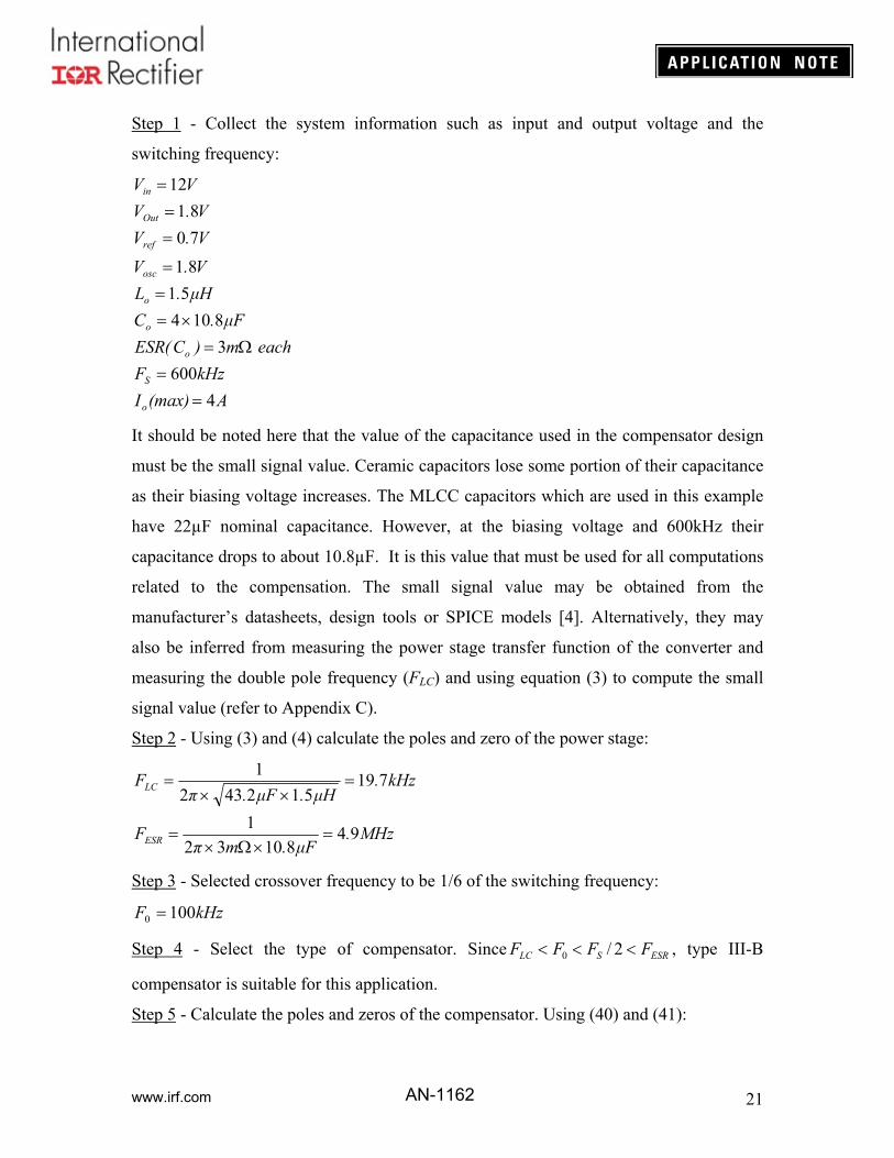
Step 1 - Collect the system information such as input and output voltage and the
switching frequency:
A(max)I
kHzF
eachm)C(ESR
Fμ.C
Hμ.L
V.V
V.V
V.V
VV
o
S
o
o
o
osc
ref
Out
in
4
600
3
8104
51
81
70
81
12
It should be noted here that the value of the capacitance used in the compensator design
must be the small signal value. Ceramic capacitors lose some portion of their capacitance
as their biasing voltage increases. The MLCC capacitors which are used in this example
have 22µF nominal capacitance. However, at the biasing voltage and 600kHz their
capacitance drops to about 10.8µF. It is this value that must be used for all computations
related to the compensation. The small signal value may be obtained from the
manufacturer’s datasheets, design tools or SPICE models [4]. Alternatively, they may
also be inferred from measuring the power stage transfer function of the converter and
measuring the double pole frequency (FLC) and using equation (3) to compute the small
signal value (refer to Appendix C).
Step 2 - Using (3) and (4) calculate the poles and zero of the power stage:
MHz.Fμ.mπ
F
kHz.Hμ.Fμ.π
F
ESR
LC
9481032
1
719512432
1
Step 3 - Selected crossover frequency to be 1/6 of the switching frequency:
kHzF 1000
Step 4 - Select the type of compensator. Since ESRSLC FFFF 2/0 , type III-B
compensator is suitable for this application.
Step 5 - Calculate the poles and zeros of the compensator. Using (40) and (41):

www.irf.com 22AN-1162
kHz.Sin
SinkHzFZ 617
701
7011002
kHzSin
SinkHzFp 567
701
7011002
Using (42):
kHz.kHz..FZ 88617501
Using (39):
kHz/kHzFp 30026003
Step 6 - Calculate the values of the parameters of the compensator. Choose nFC 2.23f .
Using (33):
6127567222
13f .
knF.πR
Choose 1273fR . Use (34) to calculate 1fR :
k.k.n.π
R 983127617222
11f
Select k.R 0241f . Using (14), 2fR can be calculated:
k.)V.V.(
V.k.R 562
7081
700242f
Choose k.R 552f2 . Use (35) to calculate 1CR :
k.
n.
.μ.μ.kπRC 772
2212
812435110021
Choose k.RC 7421 . Use (36) to calculate 1CC :
nF.k.k.π
CC 66887422
11
Choose nFCC 8.61 . Use (37) to calculate 2CC :
pFkk.π
CC 1933007422
12
Choose pFCC 1802 . The bode plot of the loop has been sketched in Figure 8 which
shows the closed loop system has a crossover frequency of kHzF 1050 and the phase-
margin of about 51º.

www.irf.com 23AN-1162
Figure 8 - The bode plot of the loop for the example with Type III-B compensator
6. Conclusion
The control loop design based on regular voltage-mode error-amplifier was discussed for
synchronous buck converter. When electrolytic capacitor or low performance tantalum
capacitors are used a simple type II compensator can be employed. For ceramic, or high
performance POS-cap or SP-Cap output capacitors, a type III compensator is usually
required. Although IR3840 and IR3842 regulators were taken as examples in this
application note, the proposed design method also applies to applications using other
types of buck regulator/control ICs which utilize a voltage-mode error-amplifier.
References
[1] M. Qiao, P. Parto, and R. Amirani, “Stabilize the Buck Converter with Transconductance
Amplifier,” IR-application note AN-1043, 2002.
[2] Ned Mohan, Tore M. Undeland, and William P. Robbins, Power Electronics: Converters,
Applications, and Design, New York: John Wiley & Sons, ISBN: 0-471-22693-9, 2003.
[3] R. W. Erickson, D. Maksimovic, Fundamentals of Power Electronics, New York: Springer
Science + Business Media, ISBN: 978-0-7923-7270-7, 2001.
[4] P. Asadi, Y. Chen, P. Parto, “Optimal Utilization of Multi Layer Ceramic Capacitors for
Synchronous Buck Converters in Point of Load Applications”, PCIM China, Shanghai,
China, June 2010, pp. 233-237.
www.irf.com 24AN-1162
Appendix A: Designing the Power Stage of the Synchronous Buck Converter
The first step in designing a switching DC/DC converter is designing the power stage.
The power stage includes the output LC filter of the converter as well as the switches and
their drivers. Many factors are involved in designing the power stage including,
efficiency, cost, space, EMI, acceptable output voltage ripple, transient response
requirement, etc. The design requirements usually compete with each other. For example,
to decrease the output voltage ripple the designer might increase the value of the inductor
and/or capacitor. Increasing the value of the capacitor increases the cost and increasing
the value of the inductor can decrease the efficiency and can make the transient response
slower. On the other hand, the output voltage ripple can be decreased by increasing the
switching frequency. However, higher switching frequency may result in less efficiency
due to increased switching losses. Therefore, the designer has to find a trade off between
different design requirements by going through a few design iterations.
Switching frequency is usually the first parameter which is selected. In selecting the
switching frequency different factors including efficiency, EMI requirements, required
closed-loop bandwidth, etc are involved. The switching frequency might even be dictated
by the system that the converter is going to be a part of.
In this appendix the procedure of designing the power stage is briefly discussed with an
example.
Suppose that the switching frequency as well as the maximum output current and the
input and output voltages are given. Depending on the maximum output current the
appropriate switching regulator is selected. The list of IR’s integrated switching
regulators and their specifications can be found on IR’s website. Among the design
requirements, usually the inductor ripple current is given. If not, starting with a 40%
current ripple is reasonable:
Max_LoadLripple I%I 40 (A1)
The inductor value can be calculated using the following equation:
Sin
out
Lripple
outino FV
V
I
VVL
1
(A2)

www.irf.com 25AN-1162
The amplitude of the overshoot/undershoot of the transient response of the converter as
well as the output voltage ripple determine the value of the output capacitor. The
amplitude of the switching ripple is usually much smaller than the permissible value if an
appropriate output capacitor combination is utilized. The minimum required amount of
output capacitor is given by the following equation:
Max_outout
Step_LoadoMin_o VV
ILC
2
2
(A3)
where Step_LoadI is the maximum step load in Amps and Max_outV is the maximum
permissible output voltage change due to transients/switching. Equation (A3) is based on
having ideal output capacitors (no ESR) and infinite control-loop band-width. The
required amount of output capacitance is usually higher than the value given by (A3)
especially when the output capacitors have a considerable amount of ESR. However, the
value calculated by (A3) is a good starting point to choose the output capacitor. Suppose
the designer intends to use a type of capacitor with the value of EC . If the ESR of the
capacitor could be neglected, the number of capacitors which is required would have
been:
EMin_oMin CC)ESR(N 0 (A4)
However, if each capacitor has an ESR equal to EESR , the minimum number of required
capacitors to have a satisfactory transient response is:
2
2)CESR
V
IL(
VLC
VI
V
ESRN EE
out
Step_Loado
Max_outoE
outStep_Load
Max_out
EMin
(A5)
Usually the first integer which is greater than the value given by (A5) should be
considered. For more information about (A5) refer to [A1].
The input capacitor of the converter should be able to handle the input current ripple:
)D(DII Max_Loadripple_in 1 (A6)
where D is the duty cycle of the converter. If the input capacitor is comprised of multiple
capacitors connected in parallel, we have:
in_Einin CNC (A7)
www.irf.com 26AN-1162
If the current ripple that each of the capacitors can handle is given by max_ripple_CI , then the
number of capacitors which should be parallel to form inC are:
max_ripple_C
ripple_inin I
IN (A8)
It is worth mentioning that values of capacitors change as temperature, bias voltage, and
operating frequency change. For example MLCC capacitors lose a considerable portion
of their capacitance as their bias voltage is increased. Therefore, in all calculations
throughout this document the effective value of the capacitors at the given operating
condition should be considered.
Design example of power stage
Consider the following data is given:
A.I
mVV
AI
AI
KHzF
V.V
VV
Lripple
Max_out
Step_Load
Max_Load
S
out
in
554
54
6
12
600
81
12
(A9)
Using (A2) the value of the inductor is calculated:
nHK
.
.
.Lo 560
600
1
12
81
554
8112
(A10)
Using (A3) the minimum required output capacitance is calculated:
Fμm.
nC Min_o 103
54812
6560 2
(A11)
Suppose the following capacitors are going to be used:
mESR
FμC
E
E
12
330 (A12)
Since Min_oE CC , it seems that one capacitor should be enough, however using (A5)
suggests:
www.irf.com 27AN-1162
71)3301281
6560(
545603302
816
54
12 2 .μm.
n
mnμ
.
m
mNMin
(A13)
Therefore, 2 capacitors with the specifications given in (A12) should be used:
mm
ESR
FμFμCo
62
12
6603302 (A14)
Suppose the capacitors which are going to be used in input side are 3.3µF capacitors
which can handle a maximum of 1.3A. The input current ripple is:
Arms.)/.(/.I ripple_in 28412811128112 (A15)
3341284 ../.Nin (A16)
Therefore, the minimum numbers of capacitors which should be paralleled at the input
are 4 capacitors.
References:
[A1] C. Qiao, J. Zhang, P. Parto, and D. Jauregui, “Output Capacitor Comparison for Low
Voltage High Current Applications,” in Proc. IEEE 35th Power Electronics Specialists
Conference, Aachen, Germany, June 2004, pp. 622-628.
www.irf.com 28AN-1162
Appendix B: Some Special Cases of Compensator Design
The guidelines provided earlier in this document on compensator design are general
guidelines which result in appropriate values for the compensator parameters in most
cases. However, sometimes fine tuning might be desirable. That is, the designer might
want to adjust the locations of the zeros and poles of the compensator (by a few design
iterations) to get better/optimized results. There might be extreme conditions where fine
tuning is necessary. In this appendix, one extreme condition in which the designer must
adjust the compensation is discussed by an example.
In some extreme conditions, the values of inductor and capacitor in the power stage may
become too large so that the resonance frequency, LCF , becomes too low compared to the
cross over frequency ( 0F ). In such conditions, if the compensator type III-B is used, the
resulting bode-plot of the loop might not be appropriate. Therefore, some modifications
in the design procedure are required. Such cases are demonstrated by an example.
Consider a synchronous buck converter with the parameters given by (B1). The designer
has been conservative in keeping the inductor current ripple and output voltage
ripple/transient very low.
kHzF
AI
KHzF
eachm)C(ESR
FμC
mR
Hμ.L
V.V
V.V
V.V
VV
Max_O
S
o
o
Lo
o
osc
ref
out
in
100
2
600
3
479
13
74
81
70
52
16
0
(B1)
At the specified output voltage, the effective value of each output capacitor is about
16µF. Therefore:

www.irf.com 29AN-1162
kHz.FμHμ.π
FLC 126169742
1
(B2)
M.mFμπ
FESR 333162
1 (B3)
Since ESRSLC F/FFF 20 , type III-B compensator is used.
Using (39)-(42) the poles and zeros of the compensator are calculated as follows:
kHz.Sin
SinkHzFZ 617
701
7011002
(B4)
kHzSin
SikHzFp 567
701
70n11002
(B5)
kHz.kHz..FZ 88617501 (B6)
kHz/kHzFp 30026003 (B7)
Now the values of the parameters of the compensator are calculated. If the value of
nF.22 is selected for 3fC , the following values are resulted:
127567222
13f knF.π
R (B8)
k.k.n.π
R 024127617222
11f (B9)
k.
n.
.μμ.kπRC 521
2216
811447410021 (B10)
nF.k.k.π
CC 820521882
11
(B11)
pFkk.π
CC 243005212
12
(B12)
It is noticed that the value of 1CR is relatively large (>20kΩ) whereas 1CC and 2CC are
relatively small. If a larger value for 3fC had been chosen, more reasonable values for
1CR , 1CC , and 2CC would have been resulted. Apart from this, considering the bode plot
of the loop, which is obtained by simulation and is presented in Figure B1, it is clear that
the behavior of the phase of the loop is not appropriate. The phase drops to below 0º at
about 9kHz which makes the system conditionally stable.

www.irf.com 30AN-1162
It should be noted that the bode-plot sketched in Figure B1 is based on the average model
for the buck converter. Therefore, it is valid only up to half of the switching frequency.
95,700-60
-50
-40
-30
-20
-10
0
10
20
30
40
50
60
70
80
100 1,000 10,000 100,000 1,000,000
Frequency (Hz)
Gai
n (
db
)
-180
-150
-120
-90
-60
-30
0
30
60
90
120
150
180
Ph
ase
(Deg
ree)
Figure B1 - The bode plot of the loop for the example with Type III-B compensator
shows a bandwidth of 95.7kHz and a phase margin of 50º
The reason for the phase drop at about 9kHz is that the pole and zero selection has been
done to secure enough phase-margin at the loop cross-over frequency. The cross-over
frequency is much higher than the resonance frequency ( LCF or double-pole frequency).
Consequently, both zeros of the compensator are above the resonance frequency where
the double pole causes 180 degrees phase-drop. Technically, it is required to have the
zeros at about LCF or even at lower frequencies. Therefore, when the procedure of type
III-B compensator design is followed, if the calculated zeros of the compensator are both
above LCF , modifications in the procedure are required as follows:
- Design for lower loop Bandwidth (1/10 of the switching frequency).
- Place the zeros of the compensator according to type III-A compensator design
procedure.
There are two reasons to design for lower loop bandwidth. First, due to relatively large
value of the selected output capacitors, usually there is no need to design for a high loop
www.irf.com 31AN-1162
bandwidth to achieve satisfactory transient response. Second, when the resonance
frequency of the regulator is much lower than the designed loop bandwidth, a relatively
high gain-bandwidth is demanded from the error amplifier. Therefore, to avoid running
into the gain-bandwidth-product limitation of the error amplifier, it is recommended to
design for a lower loop bandwidth. In this case, we design the loop for a BW of 60kHz.
Placing the zeros of the compensator according to the type III-A compensator design
procedure, moves the zeros to lower frequencies. This, in turn, reduces the gain at low
frequencies. However, according to Figure B1, the low-frequency gain is relatively large
(G(100Hz)>60dB), therefore, reducing the low-frequency gain is acceptable. Equations
(B5) or (41) can still be used to calculate the location of the second pole of the
compensator. The poles and zeros of the compensator which is going to be designed are:
kHz.FZ 262 (B13)
kHzFp 3402 (B14)
kHz.kHz..FZ 654267501 (B15)
kHz/kHzFp 30026003 (B16)
The design procedure is started with nF.C 223f . Now, the values of the components
can be calculated:
pFC
nF.C
k.R
k.R
k.R
R
nF.C
C
C
C
f
f
f
f
43
72
412
424
511
215
22
2
1
1
2
1
3
3
(B17)
With the above component values for the compensator, the bode plot of the loop is
measured and presented in Figure B2. The bode plot shows that the phase-dip around
9kHz does not go below 45º and the phase margin has increased by 9º.

www.irf.com 32AN-1162
Figure B2 - The bode plot of the loop for the example with modified Type III compensator shows a bandwidth of 62kHz and a phase margin of 59º
www.irf.com 33AN-1162
Appendix C: Loop Response Measurement
A properly measured loop response will allow measurement of control bandwidth and
phase margin. In addition, it allows estimation of actual or effective output capacitance in
a circuit. Control bandwidth indicates the speed of the system in responding to load
transients and phase margin is a very important indication of robustness of stability of the
closed loop system.
A PWM DC-DC converter exhibits time-varying effects above half of the switching
frequency and any measurements at such frequencies have no basis for comparison with
averaged model designs and predictions which do not account for the time-varying
effects. This implies that it does not serve any purpose to measure the loop response at
frequencies approaching or exceeding half of the switching frequency.
At very low frequencies and at very high frequencies, the measurement is susceptible to
noise, because of the very high and very low loop gains respectively. For typical values
of L and C used in POL designs, the LC resonant poles lie between 1 kHz and 30 kHz,
and any loop measurement must clearly show this region. For a switching frequency of
600 kHz, used in IR’s integrated buck regulator designs (SupIRBuckTM) for most POL
applications, loop response measurement in the range of 1kHz -150 kHz is sufficient.
Figure C1 shows the general schematic for a family of SupIRBucks. This schematic is
used to show how the loop response in measured. The measurement technique can
similarly be used for any other IR’s SupIRBucks. The three test points (A, B, and C)
which are used for loop-response measurement have been indicated by solid circles. To
measure the loop response the following steps should be taken:
• Using a network analyzer, apply a 15mV-30mV perturbation signal between test
points A and B.
• Set up the network analyzer to measure v(B)/v(A).
• Set the frequency range of measurement between 1 kHz and 150 kHz.
• Measure the control bandwidth as the frequency at which the loop gain response
crosses 0 dB.

www.irf.com 34AN-1162
• Measure the phase margin as the loop phase response at the loop gain crossover
frequency.
Seq./VDDQ
1
+ C21 + C22
Vin
C140.1uFC31
0.1uF
Vcc-
1
C10
L1
1 2
R28
C24
C26
C130.1uF
R19
R14
Vout
Vcc+
1
C2C5
R9
R1
R10
0
C3
R16
R3
R4R2
C4
Q1
C15
R6
C16
C25
C17
R12
C9
C18C19C20
VCC
U1
IR384x/3xE
nabl
e14
Bo
ot13
AG
nd2
15
SW11
PG
ood
8
COMP3
OC
set
7
PGnd10
SS6
Seq/Vp1
FB2
AGnd14
Vcc
9
Vin12
Rt5
R18
+C1
C27
VCC
C8
C70.1uF
VCC
R15
C28C29C30
R17
C11
C6
A B
C
Figure C1 - The typical schematic of a family of IR’s SupIRBucks and the associated test points which are used for frequency response measurements.
Figure C2 shows the result of a typical frequency response measurement. The figure
shows that the control loop bandwidth is 100.98kHz and the phase-margin is 47.975º.
Control bandwidth=100.98 kHz Phase margin=47.9750
Figure C2 - The result of loop frequency-response measurement for a typical POL application which is the amplitude and phase of v(B)/v(A) versus frequency

www.irf.com 35AN-1162
Ideally the loop frequency response should not depend on the output current of the rail.
However, due to the dead-times of the switches and some other factors, the frequency
response changes with load current to some extent. Usually the loop response should be
measured at nominal current of the rail. In addition, at the current that the loop response
is measured the converter must operate without jitter.
Another frequency response which provides useful information is the power stage
frequency response. To measure the frequency response of the power stage the following
procedure should be followed:
• Using a network analyzer, apply a 15mV-30mV perturbation signal between test
points A and B.
• Set up the network analyzer to measure v(B)/v(C).
• Set the frequency range of measurement between 1 kHz and 150 kHz.
• Measure the resonant frequency fLC of the LC output filter.
• Measure the amplitude of the frequency response at low frequencies
(G_Power_Stage_DC). This value is measured in dB scale.
• With L known, compute the effective value of output capacitance using (C1).
• Use (C2) to estimate the amplitude of the ramp signal in the modulator.
LfπC
LC
o 224
1 (C1)
)DC_Stage_Power_G
(osc
VinV
2010
(C2)
Using (C1) the effective / small-signal value of the output capacitance is obtained. This
value should be used in all computations related to compensator design. Obtaining the
effective value of the output capacitance is especially important when ceramic capacitors
are used, since ceramic capacitors considerably loose their capacitance as bias voltage is
increased. The small signal value of the output capacitors may also be obtained from the
manufacturer’s datasheets and design tools. The amplitude of the ramp signal, oscV , is
also required in the process of compensator design. This value can be obtained from the
datasheet as well. Figure C3 shows the frequency response of a typical power stage.

www.irf.com 36AN-1162
Figure C3 - The frequency response of a typical power stage showing the resonance frequency
If, for instance, a 1µH inductor is used, the effective value of the output capacitance is:
F104H1(15.61kHz)4π
122
μμ
Co (C3)
Figure C3 shows that at low frequencies the gain of the power stage is about 16.98dB.
Therefore, assuming the input voltage is 12V, the amplitude of the ramp signal will be:
V.Vosc 71
10
12)
20
16.98(
(C4)