Application Note 898 Audio Amplifiers Utilizing: … Peak Instantaneous Temperature Limiting (SPiKe)...
10
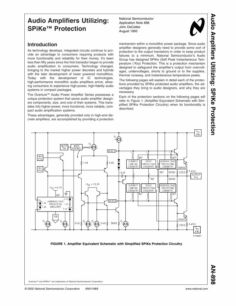
Audio Amplifiers Utilizing: SPiKe ™ Protection Introduction As technology develops, integrated circuits continue to pro- vide an advantage to consumers requiring products with more functionality and reliability for their money. It’s been less than fifty years since the first transistor began to provide audio amplification to consumers. Technology changed, bringing to the market higher power discretes and hybrids with the later development of lower powered monolithics. Today with the development of IC technologies, high-performance monolithic audio amplifiers arrive, allow- ing consumers to experience high-power, high-fidelity audio systems in compact packages. The Overture™ Audio Power Amplifier Series possesses a unique protection system that saves audio amplifier design- ers components, size, and cost of their systems. This trans- lates into higher-power, more functional, more reliable, com- pact audio amplification systems. These advantages, generally provided only in high-end dis- crete amplifiers, are accomplished by providing a protection mechanism within a monolithic power package. Since audio amplifier designers generally need to provide some sort of protection to the output transistors in order to keep product failures to a minimum, National Semiconductor’s Audio Group has designed SPiKe (Self Peak Instantaneous Tem- perature (˚Ke)) Protection. This is a protection mechanism designed to safeguard the amplifier’s output from overvolt- ages, undervoltages, shorts to ground or to the supplies, thermal runaway, and instantaneous temperature peaks. The following pages will explain in detail each of the protec- tions provided by SPiKe protected audio amplifiers, the ad- vantages they bring to audio designers, and why they are necessary. Each of the protection sections on the following pages will refer to Figure 1. (Amplifier Equivalent Schematic with Sim- plified SPiKe Protection Circuitry) when its functionality is described. Overture™ and SPiKe™ are trademarks of National Semiconductor Corporation. 01186901 FIGURE 1. Amplifier Equivalent Schematic with Simplified SPiKe Protection Circuitry National Semiconductor Application Note 898 John DeCelles August 1993 Audio Amplifiers Utilizing: SPiKe Protection AN-898 © 2002 National Semiconductor Corporation AN011869 www.national.com
Transcript of Application Note 898 Audio Amplifiers Utilizing: … Peak Instantaneous Temperature Limiting (SPiKe)...
Audio Amplifiers Utilizing:SPiKe™ Protection
IntroductionAs technology develops, integrated circuits continue to pro-vide an advantage to consumers requiring products withmore functionality and reliability for their money. It’s beenless than fifty years since the first transistor began to provideaudio amplification to consumers. Technology changed,bringing to the market higher power discretes and hybridswith the later development of lower powered monolithics.Today with the development of IC technologies,high-performance monolithic audio amplifiers arrive, allow-ing consumers to experience high-power, high-fidelity audiosystems in compact packages.
The Overture™ Audio Power Amplifier Series possesses aunique protection system that saves audio amplifier design-ers components, size, and cost of their systems. This trans-lates into higher-power, more functional, more reliable, com-pact audio amplification systems.
These advantages, generally provided only in high-end dis-crete amplifiers, are accomplished by providing a protection
mechanism within a monolithic power package. Since audioamplifier designers generally need to provide some sort ofprotection to the output transistors in order to keep productfailures to a minimum, National Semiconductor’s AudioGroup has designed SPiKe (Self Peak Instantaneous Tem-perature (˚Ke)) Protection. This is a protection mechanismdesigned to safeguard the amplifier’s output from overvolt-ages, undervoltages, shorts to ground or to the supplies,thermal runaway, and instantaneous temperature peaks.
The following pages will explain in detail each of the protec-tions provided by SPiKe protected audio amplifiers, the ad-vantages they bring to audio designers, and why they arenecessary.
Each of the protection sections on the following pages willrefer to Figure 1. (Amplifier Equivalent Schematic with Sim-plified SPiKe Protection Circuitry) when its functionality isdescribed.
Overture™ and SPiKe™ are trademarks of National Semiconductor Corporation.
01186901
FIGURE 1. Amplifier Equivalent Schematic with Simplified SPiKe Protection Circuitry
National SemiconductorApplication Note 898John DeCellesAugust 1993
Audio
Am
plifiersU
tilizing:S
PiK
eP
rotectionA
N-898
© 2002 National Semiconductor Corporation AN011869 www.national.com
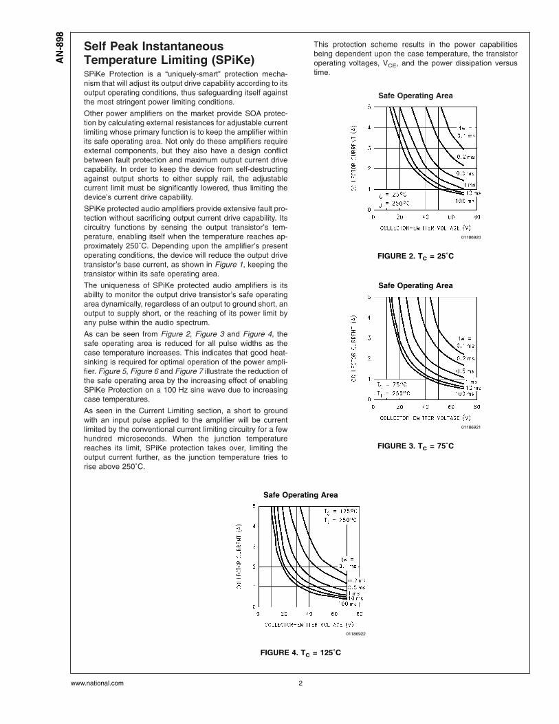
Self Peak InstantaneousTemperature Limiting (SPiKe)SPiKe Protection is a “uniquely-smart” protection mecha-nism that will adjust its output drive capability according to itsoutput operating conditions, thus safeguarding itself againstthe most stringent power limiting conditions.
Other power amplifiers on the market provide SOA protec-tion by calculating external resistances for adjustable currentlimiting whose primary function is to keep the amplifier withinits safe operating area. Not only do these amplifiers requireexternal components, but they aiso have a design conflictbetween fault protection and maximum output current drivecapability. In order to keep the device from self-destructingagainst output shorts to either supply rail, the adjustablecurrent limit must be significantly lowered, thus limiting thedevice’s current drive capability.
SPiKe protected audio amplifiers provide extensive fault pro-tection without sacrificing output current drive capability. Itscircuitry functions by sensing the output transistor’s tem-perature, enabling itself when the temperature reaches ap-proximately 250˚C. Depending upon the amplifier’s presentoperating conditions, the device will reduce the output drivetransistor’s base current, as shown in Figure 1, keeping thetransistor within its safe operating area.
The uniqueness of SPiKe protected audio amplifiers is itsabillty to monitor the output drive transistor’s safe operatingarea dynamically, regardless of an output to ground short, anoutput to supply short, or the reaching of its power limit byany pulse within the audio spectrum.
As can be seen from Figure 2, Figure 3 and Figure 4, thesafe operating area is reduced for all pulse widths as thecase temperature increases. This indicates that good heat-sinking is required for optimal operation of the power ampli-fier. Figure 5, Figure 6 and Figure 7 illustrate the reduction ofthe safe operating area by the increasing effect of enablingSPiKe Protection on a 100 Hz sine wave due to increasingcase temperatures.
As seen in the Current Limiting section, a short to groundwith an input pulse applied to the amplifier will be currentlimited by the conventional current limiting circuitry for a fewhundred microseconds. When the junction temperaturereaches its limit, SPiKe protection takes over, limiting theoutput current further, as the junction temperature tries torise above 250˚C.
This protection scheme results in the power capabilitiesbeing dependent upon the case temperature, the transistoroperating voltages, VCE, and the power dissipation versustime.
Safe Operating Area
01186920
FIGURE 2. TC = 25˚C
Safe Operating Area
01186921
FIGURE 3. TC = 75˚C
Safe Operating Area
01186922
FIGURE 4. TC = 125˚C
AN
-898
www.national.com 2
Self Peak InstantaneousTemperature Limiting (SPiKe)(Continued)
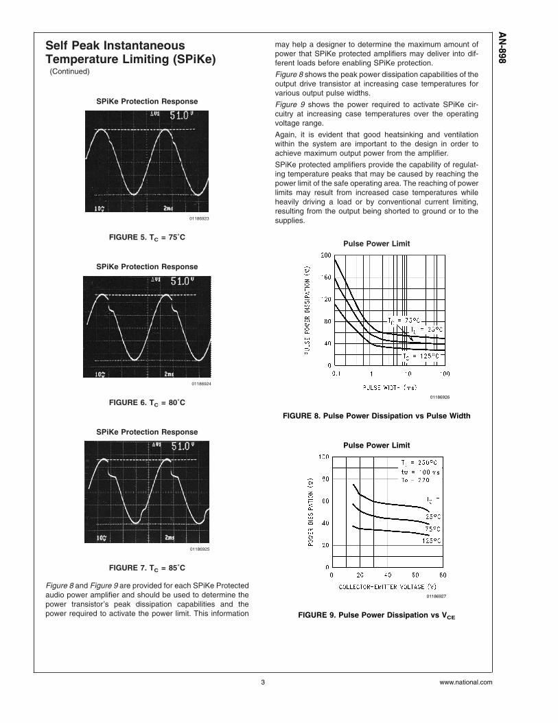
Figure 8 and Figure 9 are provided for each SPiKe Protectedaudio power amplifier and should be used to determine thepower transistor’s peak dissipation capabilities and thepower required to activate the power limit. This information
may help a designer to determine the maximum amount ofpower that SPiKe protected amplifiers may deliver into dif-ferent loads before enabling SPiKe protection.
Figure 8 shows the peak power dissipation capabilities of theoutput drive transistor at increasing case temperatures forvarious output pulse widths.
Figure 9 shows the power required to activate SPiKe cir-cuitry at increasing case temperatures over the operatingvoltage range.
Again, it is evident that good heatsinking and ventilationwithin the system are important to the design in order toachieve maximum output power from the amplifier.
SPiKe protected amplifiers provide the capability of regulat-ing temperature peaks that may be caused by reaching thepower limit of the safe operating area. The reaching of powerlimits may result from increased case temperatures whileheavily driving a load or by conventional current limiting,resulting from the output being shorted to ground or to thesupplies.
SPiKe Protection Response
01186923
FIGURE 5. TC = 75˚C
SPiKe Protection Response
01186924
FIGURE 6. TC = 80˚C
SPiKe Protection Response
01186925
FIGURE 7. TC = 85˚C
Pulse Power Limit
01186926
FIGURE 8. Pulse Power Dissipation vs Pulse Width
Pulse Power Limit
01186927
FIGURE 9. Pulse Power Dissipation vs VCE
AN
-898
www.national.com3
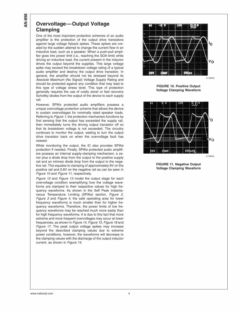
Overvoltage—Output VoltageClampingOne of the most important protection schemes of an audioamplifier is the protection of the output drive transistorsagainst large voltage flyback spikes. These spikes are cre-ated by the sudden attempt to change the current flow in aninductive load, such as a speaker. When a push-pull ampli-fier goes into power limit (i.e., reaching the SOA limit) whiledriving an inductive load, the current present in the inductordrives the output beyond the supplies. This large voltagespike may exceed the breakdown voltage rating of a typicalaudio amplifier and destroy the output drive transistor. Ingeneral, the amplifier should not be stressed beyond itsAbsolute Maximum (No Signal) Voltage Supply Rating andshould be protected against any condition that may lead tothis type of voltage stress level. This type of protectiongenerally requires the use of costly zener or fast recoverySchottky diodes from the output of the device to each supplyrail.
However, SPiKe protected audio amplifiers possess aunique overvoltage protection scheme that allows the deviceto sustain overvoltages for nominally rated speaker loads.Referring to Figure 1, the protection mechanism functions byfirst sensing that the output has exceeded the supply rail,then immediately turns the driving output transistor off sothat its breakdown voltage is not exceeded. The circuitrycontinues to monitor the output, waiting to turn the outputdrive transistor back on when the overvoltage fault hasceased.
While monitoring the output, the IC also provides SPiKeprotection if needed. Finally, SPiKe protected audio amplifi-ers possess an internal supply-clamping mechanism; a ze-ner plus a diode drop from the output to the positive supplyrail and an intrinsic diode drop from the output to the nega-tive rail. This equates to clamping of approximately 8V on thepositive rail and 0.8V on the negative rail as can be seen inFigure 10 and Figure 11, respectively.
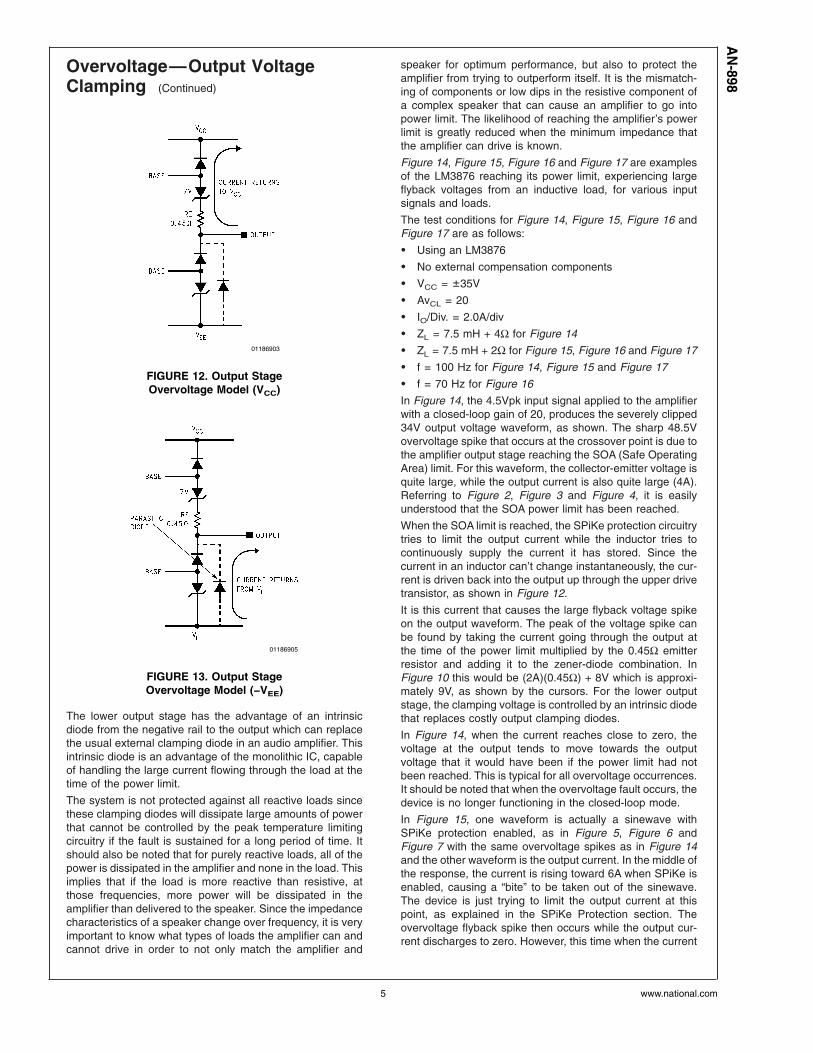
Figure 12 and Figure 13 model the output stage for eachovervoltage condition exemplifying how the voltage wave-forms are clamped to their respective values for high fre-quency waveforms. As shown in the Self Peak Instanta-neous Temperature Limiting (SPiKe) section, Figure 2,Figure 3 and Figure 4, the safe operating area for lowerfrequency waveforms is much smaller than for higher fre-quency waveforms. Therefore, the power limits of low fre-quency waveforms may be reached much more easily thanfor high frequency waveforms. It is due to this fact that moreextreme and more frequent overvoltages may occur at lowerfrequencies, as shown in Figure 14, Figure 15, Figure 16 andFigure 17. The peak output voltage spikes may increasebeyond the described clamping values due to extremepower conditions, however, the waveforms will decrease tothe clamping values with the discharge of the output inductorcurrent, as shown in Figure 14.
01186902
FIGURE 10. Positive OutputVoltage Clamping Waveform
01186904
FIGURE 11. Negative OutputVoltage Clamping Waveform
AN
-898
www.national.com 4
Overvoltage—Output VoltageClamping (Continued)
The lower output stage has the advantage of an intrinsicdiode from the negative rail to the output which can replacethe usual external clamping diode in an audio amplifier. Thisintrinsic diode is an advantage of the monolithic IC, capableof handling the large current flowing through the load at thetime of the power limit.
The system is not protected against all reactive loads sincethese clamping diodes will dissipate large amounts of powerthat cannot be controlled by the peak temperature limitingcircuitry if the fault is sustained for a long period of time. Itshould also be noted that for purely reactive loads, all of thepower is dissipated in the amplifier and none in the load. Thisimplies that if the load is more reactive than resistive, atthose frequencies, more power will be dissipated in theamplifier than delivered to the speaker. Since the impedancecharacteristics of a speaker change over frequency, it is veryimportant to know what types of loads the amplifier can andcannot drive in order to not only match the amplifier and
speaker for optimum performance, but also to protect theamplifier from trying to outperform itself. It is the mismatch-ing of components or low dips in the resistive component ofa complex speaker that can cause an amplifier to go intopower limit. The likelihood of reaching the amplifier’s powerlimit is greatly reduced when the minimum impedance thatthe amplifier can drive is known.
Figure 14, Figure 15, Figure 16 and Figure 17 are examplesof the LM3876 reaching its power limit, experiencing largeflyback voltages from an inductive load, for various inputsignals and loads.
The test conditions for Figure 14, Figure 15, Figure 16 andFigure 17 are as follows:
• Using an LM3876
• No external compensation components
• VCC = ±35V
• AvCL = 20
• IO/Div. = 2.0A/div
• ZL = 7.5 mH + 4Ω for Figure 14
• ZL = 7.5 mH + 2Ω for Figure 15, Figure 16 and Figure 17
• f = 100 Hz for Figure 14, Figure 15 and Figure 17
• f = 70 Hz for Figure 16
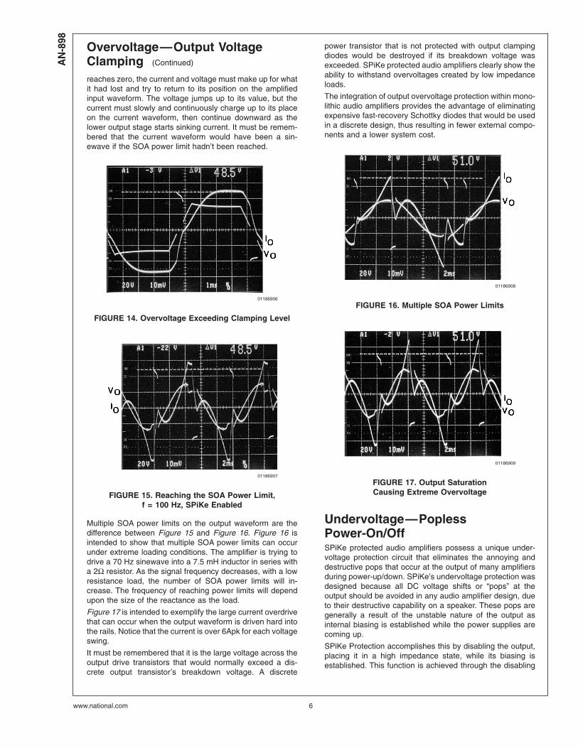
In Figure 14, the 4.5Vpk input signal applied to the amplifierwith a closed-loop gain of 20, produces the severely clipped34V output voltage waveform, as shown. The sharp 48.5Vovervoltage spike that occurs at the crossover point is due tothe amplifier output stage reaching the SOA (Safe OperatingArea) limit. For this waveform, the collector-emitter voltage isquite large, while the output current is also quite large (4A).Referring to Figure 2, Figure 3 and Figure 4, it is easilyunderstood that the SOA power limit has been reached.
When the SOA limit is reached, the SPiKe protection circuitrytries to limit the output current while the inductor tries tocontinuously supply the current it has stored. Since thecurrent in an inductor can’t change instantaneously, the cur-rent is driven back into the output up through the upper drivetransistor, as shown in Figure 12.
It is this current that causes the large flyback voltage spikeon the output waveform. The peak of the voltage spike canbe found by taking the current going through the output atthe time of the power limit multiplied by the 0.45Ω emitterresistor and adding it to the zener-diode combination. InFigure 10 this would be (2A)(0.45Ω) + 8V which is approxi-mately 9V, as shown by the cursors. For the lower outputstage, the clamping voltage is controlled by an intrinsic diodethat replaces costly output clamping diodes.
In Figure 14, when the current reaches close to zero, thevoltage at the output tends to move towards the outputvoltage that it would have been if the power limit had notbeen reached. This is typical for all overvoltage occurrences.It should be noted that when the overvoltage fault occurs, thedevice is no longer functioning in the closed-loop mode.
In Figure 15, one waveform is actually a sinewave withSPiKe protection enabled, as in Figure 5, Figure 6 andFigure 7 with the same overvoltage spikes as in Figure 14and the other waveform is the output current. In the middle ofthe response, the current is rising toward 6A when SPiKe isenabled, causing a “bite” to be taken out of the sinewave.The device is just trying to limit the output current at thispoint, as explained in the SPiKe Protection section. Theovervoltage flyback spike then occurs while the output cur-rent discharges to zero. However, this time when the current
01186903
FIGURE 12. Output StageOvervoltage Model (VCC)
01186905
FIGURE 13. Output StageOvervoltage Model (−VEE)
AN
-898
www.national.com5
Overvoltage—Output VoltageClamping (Continued)
reaches zero, the current and voltage must make up for whatit had lost and try to return to its position on the amplifiedinput waveform. The voltage jumps up to its value, but thecurrent must slowly and continuously charge up to its placeon the current waveform, then continue downward as thelower output stage starts sinking current. It must be remem-bered that the current waveform would have been a sin-ewave if the SOA power limit hadn’t been reached.
Multiple SOA power limits on the output waveform are thedifference between Figure 15 and Figure 16. Figure 16 isintended to show that multiple SOA power limits can occurunder extreme loading conditions. The amplifier is trying todrive a 70 Hz sinewave into a 7.5 mH inductor in series witha 2Ω resistor. As the signal frequency decreases, with a lowresistance load, the number of SOA power limits will in-crease. The frequency of reaching power limits will dependupon the size of the reactance as the load.
Figure 17 is intended to exemplify the large current overdrivethat can occur when the output waveform is driven hard intothe rails. Notice that the current is over 6Apk for each voltageswing.
It must be remembered that it is the large voltage across theoutput drive transistors that would normally exceed a dis-crete output transistor’s breakdown voltage. A discrete
power transistor that is not protected with output clampingdiodes would be destroyed if its breakdown voltage wasexceeded. SPiKe protected audio amplifiers clearly show theability to withstand overvoltages created by low impedanceloads.
The integration of output overvoltage protection within mono-lithic audio amplifiers provides the advantage of eliminatingexpensive fast-recovery Schottky diodes that would be usedin a discrete design, thus resulting in fewer external compo-nents and a lower system cost.
Undervoltage—PoplessPower-On/OffSPiKe protected audio amplifiers possess a unique under-voltage protection circuit that eliminates the annoying anddestructive pops that occur at the output of many amplifiersduring power-up/down. SPiKe’s undervoltage protection wasdesigned because all DC voltage shifts or “pops” at theoutput should be avoided in any audio amplifier design, dueto their destructive capability on a speaker. These pops aregenerally a result of the unstable nature of the output asinternal biasing is established while the power supplies arecoming up.
SPiKe Protection accomplishes this by disabling the output,placing it in a high impedance state, while its biasing isestablished. This function is achieved through the disabling
01186906
FIGURE 14. Overvoltage Exceeding Clamping Level
01186907
FIGURE 15. Reaching the SOA Power Limit,f = 100 Hz, SPiKe Enabled
01186908
FIGURE 16. Multiple SOA Power Limits
01186909
FIGURE 17. Output SaturationCausing Extreme Overvoltage
AN
-898
www.national.com 6
Undervoltage—PoplessPower-On/Off (Continued)
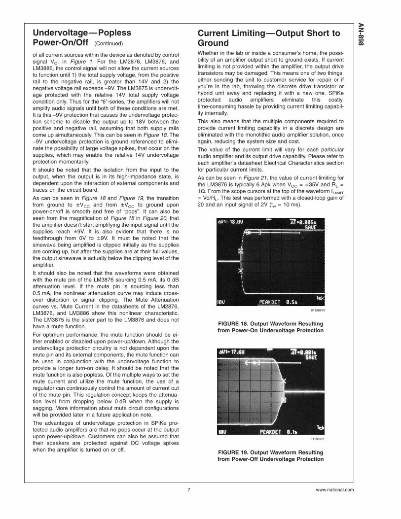
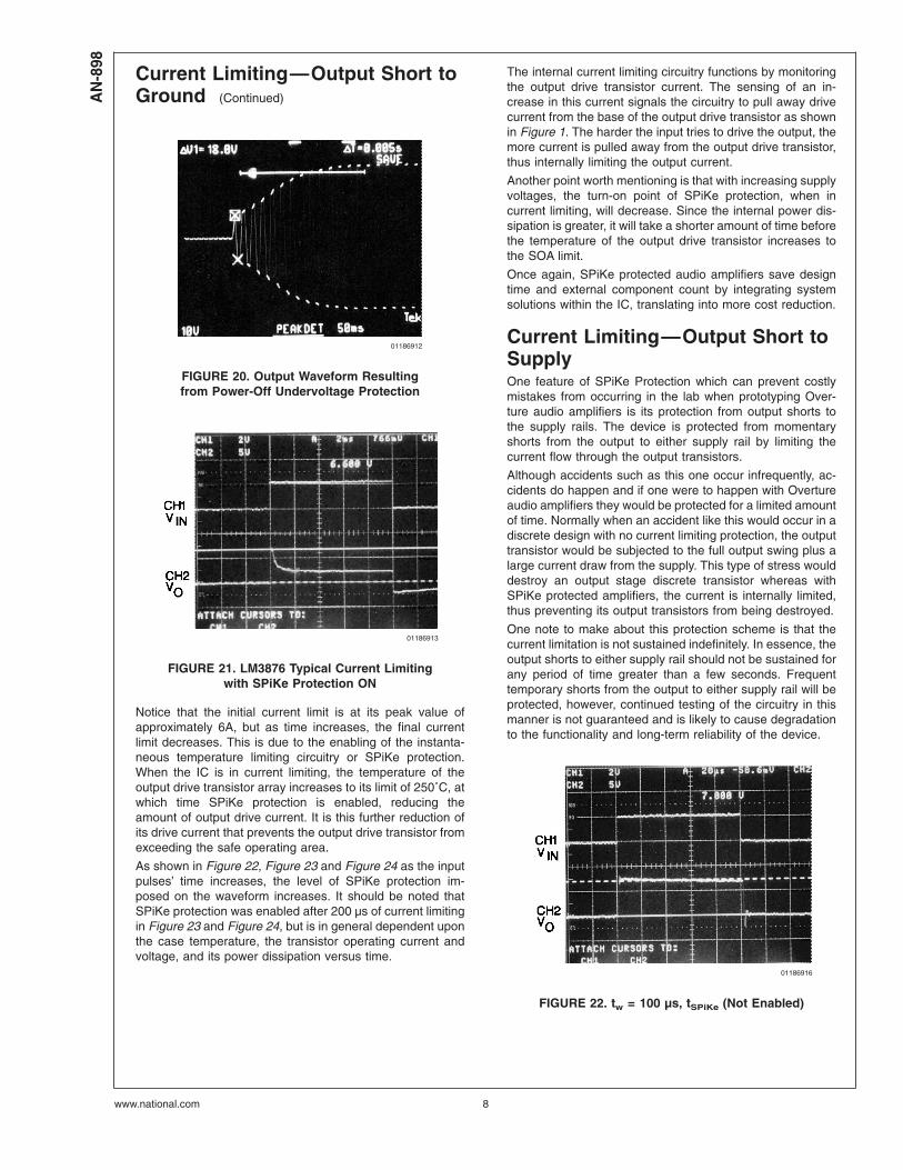
of all current sources within the device as denoted by controlsignal VC, in Figure 1. For the LM2876, LM3876, andLM3886, the control signal will not allow the current sourcesto function until 1) the total supply voltage, from the positiverail to the negative rail, is greater than 14V and 2) thenegative voltage rail exceeds −9V. The LM3875 is undervolt-age protected with the relative 14V total supply voltagecondition only. Thus for the “6”-series, the amplifiers will notamplify audio signals until both of these conditions are met.It is this −9V protection that causes the undervoltage protec-tion scheme to disable the output up to 18V between thepositive and negative rail, assuming that both supply railscome up simultaneously. This can be seen in Figure 18. The−9V undervoltage protection is ground referenced to elimi-nate the possibility of large voltage spikes, that occur on thesupplies, which may enable the relative 14V undervoltageprotection momentarily.
It should be noted that the isolation from the input to theoutput, when the output is in its high-impedance state, isdependent upon the interaction of external components andtraces on the circuit board.
As can be seen in Figure 18 and Figure 19, the transitionfrom ground to ±VCC and from ±VCC to ground uponpower-on/off is smooth and free of “pops”. It can also beseen from the magnification of Figure 18 in Figure 20, thatthe amplifier doesn’t start amplifying the input signal until thesupplies reach ±9V. It is also evident that there is nofeedthrough from 0V to ±9V. It must be noted that thesinewave being amplified is clipped initially as the suppliesare coming up, but after the supplies are at their full values,the output sinewave is actually below the clipping level of theamplifier.
It should also be noted that the waveforms were obtainedwith the mute pin of the LM3876 sourcing 0.5 mA, its 0 dBattenuation level. If the mute pin is sourcing less than0.5 mA, the nonlinear attenuation curve may induce cross-over distortion or signal clipping. The Mute Attenuationcurves vs. Mute Current in the datasheets of the LM2876,LM3876, and LM3886 show this nonlinear characteristic.The LM3875 is the sister part to the LM3876 and does nothave a mute function.
For optimum performance, the mute function should be ei-ther enabled or disabled upon power-up/down. Although theundervoltage protection circuitry is not dependent upon themute pin and its external components, the mute function canbe used in conjunction with the undervoltage function toprovide a longer turn-on delay. It should be noted that themute function is also popless. Of the multiple ways to set themute current and utilize the mute function, the use of aregulator can continuously control the amount of current outof the mute pin. This regulation concept keeps the attenua-tion level from dropping below 0 dB when the supply issagging. More information about mute circuit configurationswill be provided later in a future application note.
The advantages of undervoltage protection in SPiKe pro-tected audio amplifers are that no pops occur at the outputupon power-up/down. Customers can also be assured thattheir speakers are protected against DC voltage spikeswhen the amplifier is turned on or off.
Current Limiting—Output Short toGroundWhether in the lab or inside a consumer’s home, the possi-bility of an amplifier output short to ground exists. If currentlimiting is not provided within the amplifier, the output drivetransistors may be damaged. This means one of two things,either sending the unit to customer service for repair or ifyou’re in the lab, throwing the discrete drive transistor orhybrid unit away and replacing it with a new one. SPiKeprotected audio amplifiers eliminate this costly,time-consuming hassle by providing current limiting capabil-ity internally.
This also means that the multiple components required toprovide current limiting capability in a discrete design areeliminated with the monolithic audio amplifier solution, onceagain, reducing the system size and cost.
The value of the current limit will vary for each particularaudio amplifier and its output drive capability. Please refer toeach amplifier’s datasheet Electrical Characteristics sectionfor particular current limits.
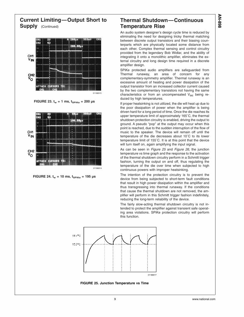
As can be seen in Figure 21, the value of current limiting forthe LM3876 is typically 6 Apk when VCC = ±35V and RL =1Ω. From the scope cursors at the top of the waveform ILIMIT
= Vo/RL. This test was performed with a closed-loop gain of20 and an input signal of 2V (tw = 10 ms).
01186910
FIGURE 18. Output Waveform Resultingfrom Power-On Undervoltage Protection
01186911
FIGURE 19. Output Waveform Resultingfrom Power-Off Undervoltage Protection
AN
-898
www.national.com7
Current Limiting—Output Short toGround (Continued)
Notice that the initial current limit is at its peak value ofapproximately 6A, but as time increases, the final currentlimit decreases. This is due to the enabling of the instanta-neous temperature limiting circuitry or SPiKe protection.When the IC is in current limiting, the temperature of theoutput drive transistor array increases to its limit of 250˚C, atwhich time SPiKe protection is enabled, reducing theamount of output drive current. It is this further reduction ofits drive current that prevents the output drive transistor fromexceeding the safe operating area.
As shown in Figure 22, Figure 23 and Figure 24 as the inputpulses’ time increases, the level of SPiKe protection im-posed on the waveform increases. It should be noted thatSPiKe protection was enabled after 200 µs of current limitingin Figure 23 and Figure 24, but is in general dependent uponthe case temperature, the transistor operating current andvoltage, and its power dissipation versus time.
The internal current limiting circuitry functions by monitoringthe output drive transistor current. The sensing of an in-crease in this current signals the circuitry to pull away drivecurrent from the base of the output drive transistor as shownin Figure 1. The harder the input tries to drive the output, themore current is pulled away from the output drive transistor,thus internally limiting the output current.
Another point worth mentioning is that with increasing supplyvoltages, the turn-on point of SPiKe protection, when incurrent limiting, will decrease. Since the internal power dis-sipation is greater, it will take a shorter amount of time beforethe temperature of the output drive transistor increases tothe SOA limit.
Once again, SPiKe protected audio amplifiers save designtime and external component count by integrating systemsolutions within the IC, translating into more cost reduction.
Current Limiting—Output Short toSupplyOne feature of SPiKe Protection which can prevent costlymistakes from occurring in the lab when prototyping Over-ture audio amplifiers is its protection from output shorts tothe supply rails. The device is protected from momentaryshorts from the output to either supply rail by limiting thecurrent flow through the output transistors.
Although accidents such as this one occur infrequently, ac-cidents do happen and if one were to happen with Overtureaudio amplifiers they would be protected for a limited amountof time. Normally when an accident like this would occur in adiscrete design with no current limiting protection, the outputtransistor would be subjected to the full output swing plus alarge current draw from the supply. This type of stress woulddestroy an output stage discrete transistor whereas withSPiKe protected amplifiers, the current is internally limited,thus preventing its output transistors from being destroyed.
One note to make about this protection scheme is that thecurrent limitation is not sustained indefinitely. In essence, theoutput shorts to either supply rail should not be sustained forany period of time greater than a few seconds. Frequenttemporary shorts from the output to either supply rail will beprotected, however, continued testing of the circuitry in thismanner is not guaranteed and is likely to cause degradationto the functionality and long-term reliability of the device.
01186912
FIGURE 20. Output Waveform Resultingfrom Power-Off Undervoltage Protection
01186913
FIGURE 21. LM3876 Typical Current Limitingwith SPiKe Protection ON
01186916
FIGURE 22. tw = 100 µs, tSPiKe (Not Enabled)
AN
-898
www.national.com 8
Current Limiting—Output Short toSupply (Continued)
Thermal Shutdown—ContinuousTemperature RiseAn audio system designer’s design cycle time is reduced byeliminating the need for designing tricky thermal matchingbetween discrete output transistors and their biasing coun-terparts which are physically located some distance fromeach other. Complex thermal sensing and control circuitryprovided from the legendary Bob Widlar, and the ability ofintegrating it onto a monolithic amplifier, eliminates the ex-ternal circuitry and long design time required in a discreteamplifier design.
SPiKe protected audio amplifiers are safeguarded fromThermal runaway, an area of concern for anycomplementary-symmetry amplifier. Thermal runaway is anexcessive amount of heating and power dissipation of theoutput transistor from an increased collector current causedby the two complementary transistors not having the samecharacteristics or from an uncompensated VBE being re-duced by high temperatures.
If proper heatsinking is not utilized, the die will heat up due tothe poor dissipation of power when the amplifier is beingdriven hard for a long period of time. Once the die reaches itsupper temperature limit of approximately 165˚C, the thermalshutdown protection circuitry is enabled, driving the output toground. A pseudo “pop” at the output may occur when thispoint is reached, due to the sudden interruption of the flow ofmusic to the speaker. The device will remain off until thetemperature of the die decreases about 10˚C to its lowertemperature limit of 155˚C. It is at this point that the devicewill turn itself on, again amplifying the input signal.
As can be seen in Figure 25 and Figure 26, the junctiontemperature vs time graph and the response to the activationof the thermal shutdown circuitry perform in a Schmitt triggerfashion, turning the output on and off, thus regulating thetemperature of the die over time when subjected to highcontinuous powers with improper heatsinking.
The intention of the protection circuitry is to prevent thedevice from being subjected to short-term fault conditionsthat result in high power dissipation within the amplifier andthus transgressing into thermal runaway. If the conditionsthat cause the thermal shutdown are not removed, the am-plifier will perform in this Schmitt trigger fashion indefinitely,reducing the long-term reliability of the device.
The fairly slow-acting thermal shutdown circuitry is not in-tended to protect the amplifier against transient safe operat-ing area violations. SPiKe protection circuitry will performthis function.
01186915
FIGURE 23. tw = 1 ms, tSPiKe = 200 µs
01186914
FIGURE 24. tw = 10 ms, tSPiKe = 195 µs
01186917
FIGURE 25. Junction Temperature vs Time
AN
-898
www.national.com9
Thermal Shutdown—Continuous Temperature Rise (Continued)
LIFE SUPPORT POLICY
NATIONAL’S PRODUCTS ARE NOT AUTHORIZED FOR USE AS CRITICAL COMPONENTS IN LIFE SUPPORTDEVICES OR SYSTEMS WITHOUT THE EXPRESS WRITTEN APPROVAL OF THE PRESIDENT AND GENERALCOUNSEL OF NATIONAL SEMICONDUCTOR CORPORATION. As used herein:
1. Life support devices or systems are devices orsystems which, (a) are intended for surgical implantinto the body, or (b) support or sustain life, andwhose failure to perform when properly used inaccordance with instructions for use provided in thelabeling, can be reasonably expected to result in asignificant injury to the user.
2. A critical component is any component of a lifesupport device or system whose failure to performcan be reasonably expected to cause the failure ofthe life support device or system, or to affect itssafety or effectiveness.
National SemiconductorCorporationAmericasEmail: [email protected]
National SemiconductorEurope
Fax: +49 (0) 180-530 85 86Email: [email protected]
Deutsch Tel: +49 (0) 69 9508 6208English Tel: +44 (0) 870 24 0 2171Français Tel: +33 (0) 1 41 91 8790
National SemiconductorAsia Pacific CustomerResponse GroupTel: 65-2544466Fax: 65-2504466Email: [email protected]
National SemiconductorJapan Ltd.Tel: 81-3-5639-7560Fax: 81-3-5639-7507
www.national.com
01186918
FIGURE 26. Thermal Shutdown Waveform
01186919
FIGURE 27. Actual Thermal Shutdown Waveform
AN
-898
Aud
ioA
mpl
ifier
sU
tiliz
ing:
SP
iKe
Pro
tect
ion
National does not assume any responsibility for use of any circuitry described, no circuit patent licenses are implied and National reserves the right at any time without notice to change said circuitry and specifications.