Application Brief GaN Switching Loss Simulation using LTSpice · circuit in LTSpice The simulation...
11
GaN Systems 1 Application Brief GaN Switching Loss Simulation using LTSpice Apr 28, 2017
Transcript of Application Brief GaN Switching Loss Simulation using LTSpice · circuit in LTSpice The simulation...

GaN Systems 1
Application BriefGaN Switching Loss Simulation using LTSpice
Apr 28, 2017

GaN Systems 2
Overview
▪ GaN Systems provides Pspice/LTSpice simulation models for GaN Enhancement
mode HEMT.
▪ In this presentation, a half bridge double pulse test circuit in LTSpice will be
introduced and used as the test bench to evaluate switching performance under
different electrical parameters.
▪ Switching losses were simulated and compared with Lab measurement

GaN Systems 3
Half Bridge Double Pulse Test bench in LTSpice
HS/LS Gate driver circuit
DUT
ID
VDS

GaN Systems 4
Half Bridge Double Pulse Test bench in LTSpice
Set up the simulation parameters:
.param VBUS = 400; DC bus voltage
.param ISW = 30; Switching Current
.param RGON =10; Turn-on Gate Resistor
.param RGOFF = 2; Turn-off Gate Resistor
.param VDRV_P = 6; Turn-on gate voltage
.param VDRV_N = 3; Turn-off negative gate voltage
.param DT = 100n; dead time
.param T_ON = 2U; Turn-on period
.param L_DPT = VBUS * (T_ON-2*DT) / ISW ; calculated L for switching current setting
.param T_P = 2.5U; total period
.param L_GATE =3N; gate inductance
.param LS_EX= 10p; external source inductance
.param L_DS =3N; power loop inductance
Switching test parameters
Parasitic Inductances
.option temp=25 ; Junction temperature setting, adjust between 25 and 150C

GaN Systems 5
Gate waveforms (Simulated vs Measured)
▪ Good correlation between simulated and measured waveforms.▪ Parasitics: L_DS = 3nH, L_GATE = 3nH
VGS-3V
6V
VSW
-7V
0V
<0V
MeasurementLTSpice SimulationVGS spike on free-wheeling
device induced by dv/dt
(miller feedback)

GaN Systems 6
Half Bridge Double Pulse Test bench in LTSpice
Double Pulse Simulation Results (400V/30A)
VDS
ID
30A Turn-off
30A Turn-on
400V/30A Hard switch-off
400V/30A Hard switch-on

GaN Systems 7
Half Bridge Double Pulse Test bench in LTSpiceSwitching Loss Calculation using LTSpice
EON = 106uJ
400V/30A Turn-on 400V/30A Turn-off
EOFF = 8uJPSW = VDS*ID
PSW = VDS*ID
GaN Systems 8
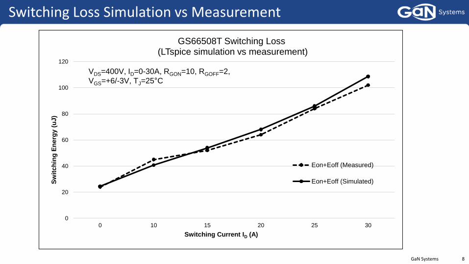
Switching Loss Simulation vs Measurement
0
20
40
60
80
100
120
0 10 15 20 25 30
Sw
itch
ing
En
erg
y (
uJ)
Switching Current ID (A)
GS66508T Switching Loss(LTspice simulation vs measurement)
Eon+Eoff (Measured)
Eon+Eoff (Simulated)
VDS=400V, ID=0-30A, RGON=10, RGOFF=2,
VGS=+6/-3V, TJ=25°C

GaN Systems 9
Simulated Switching Loss
▪ Turn-on loss increases with TJ due to the reduced trans-
conductance at higher temperature
▪ Turn-off for GaN is small and less temperature dependent
0
50
100
150
200
250
10 15 20 25 30
To
tal S
witch
ing
En
erg
y L
oss E
ON+
EO
FF
(uJ)
Switching Current ID (A)
Switching Loss vs. TJ (GS66508T)
VDS = 400V, RGON = 10Ω, RGOFF = 2Ω
0
10
20
30
40
50
60
70
80
0 5 10 15 20 25 30
Sw
itchin
g E
nerg
y (u
J)
Gate Resistance RG (Ω)
EON and EOFF vs RG (GS66508T)
VDS = 400V, ID = 15A, TJ=25°C
EON
EOFF
▪ Switching Loss increases with RG.

GaN Systems 10
Summary
▪ GaN E-HEMT switching losses were simulated by using a half bridge double pulse test circuit in LTSpice
▪ The simulation results were verified by the lab measurement. Although the real world measurement can be affected by many other factors, we have achieved reasonably good agreement between the simulation model and measurement.
▪ This LTSpice test circuit can be a convenient tool for end users to get started with simulation and be familiar with GaN switching characteristics to assist their design.
▪ This simulation test bench can also be used to easily evaluate GaN switching performance under different electrical parameters
Click to download LTSpice simulation file

GaN Systems 11
www.gansystems.com • North America • Europe • Asia
Tomorrow’s power todayTM