APPENDIX C. MICROSYSTEMS RESEARCH IN THE UNITED · PDF file132 Appendix C. Microsystems...
50
Appendix C. Microsystems Research in the United States: A Critical Overview 132 APPENDIX C. MICROSYSTEMS RESEARCH IN THE UNITED STATES: A CRITICAL OVERVIEW 1 INTRODUCTION The field of microelectromechanical systems (MEMS) has developed rapidly since its beginnings in the 1980s, with a worldwide industry becoming well established by the year 2000. The range of MEMS applications has broadened from an early focus on silicon sensors for physical variables such as pressure and acceleration, to encompass a wide range of sensing and actuating functions. Over the past five years, the technology has matured to the point where the emphasis has shifted from device technology and design to the integration of sensing, actuating, computation, and communication into a microsystem that implements a useful function. The names of two major U.S. National Science Foundation (NSF) academic research centers reflect this shift in emphasis. The Berkeley Sensor & Actuator Center (BSAC), was originally called the Berkeley Integrated Sensor Center when founded in 1986 and was renamed in 1989 with the increasing importance of silicon actuator research. The Wireless Integrated Microsystems Center (WIMS), an NSF Engineering Research Center, was founded in 2000 and is led by the University of Michigan. Although much research on the scientific fundamentals of MEMS remains to be done and the level of maturity in device technology and design models is uneven across the wide range of applications, the future of both research and commercialization lies in the creation of microsystems. Under the auspices of JTEC, Prof. Kensall Wise from the University of Michigan led a study of MEMS in Japan in 1994. The resulting report was widely circulated and had a significant impact on the research priorities of the NSF, one of the sponsors of the study. The 2001 WTEC Japan Microsystems Study is sponsored by the NSF, with additional support from the U.S. Defense Advanced Research Projects Agency (DARPA), the National Institute of Standards and Technology (NIST), and the Office of Naval Research (ONR). Both the MEMS and the microfluidic and molecular systems programs of the DARPA Microsystems Technology Office (MTO) are helping to support the study. The sponsors are interested broadly in defining the long-term research strategies for microsystems technologies, with a specific interest in the interface between the microsystems and nanotechnology fields. A sample of the microsystems applications of interest to the sponsors include the basic science foundation, bio-actuators, modeling the bio- electronic interface, microfluidics, bio-compatible microsystems materials, non-silicon microsystems fabrication, single molecule detection sensors, power issues in microsystems, wireless communications, optical communications, heterogeneous integration technologies, and self-assembly processes. Given the long-term perspective of this study, the sponsors are interested in new directions in both biological and physical microsystems research. Finally, the NSF is interested in Japanese activities in microsystems education and in encouraging interest in science and technology among pre-college students. The panel members look forward to a vigorous interchange of ideas with Japanese researchers on the future of microsystems technology, which we are confident will prove to be of mutual benefit. With the applications of microsystems in biology especially promising, we are interested in sharing perspectives on all aspects of this still largely unexplored area. Understanding the intersection between nanotechnology and microsystems technology in Japanese research strategy is a high priority. We would also like to understand the state of the infrastructure for microsystems research and development, including fabrication equipment, foundry services, design tools, and encapsulation processes. We also would like to discuss Japanese perspectives on the barriers to microsystems commercialization. Finally, the panel is interested in exploring areas where collaboration between Japanese and U.S. research efforts can prove fruitful. 1 Prior to travelling to Japan, the WTEC panel members prepared the following summary of U.S. activities in Japan. This reflects the status in the United States as of the date it was completed, in October 2001.
Transcript of APPENDIX C. MICROSYSTEMS RESEARCH IN THE UNITED · PDF file132 Appendix C. Microsystems...
Appendix C. Microsystems Research in the United States: A Critical Overview 132
APPENDIX C. MICROSYSTEMS RESEARCH IN THE UNITED STATES: A CRITICAL OVERVIEW1
INTRODUCTION
The field of microelectromechanical systems (MEMS) has developed rapidly since its beginnings in the 1980s, with a worldwide industry becoming well established by the year 2000. The range of MEMS applications has broadened from an early focus on silicon sensors for physical variables such as pressure and acceleration, to encompass a wide range of sensing and actuating functions. Over the past five years, the technology has matured to the point where the emphasis has shifted from device technology and design to the integration of sensing, actuating, computation, and communication into a microsystem that implements a useful function. The names of two major U.S. National Science Foundation (NSF) academic research centers reflect this shift in emphasis. The Berkeley Sensor & Actuator Center (BSAC), was originally called the Berkeley Integrated Sensor Center when founded in 1986 and was renamed in 1989 with the increasing importance of silicon actuator research. The Wireless Integrated Microsystems Center (WIMS), an NSF Engineering Research Center, was founded in 2000 and is led by the University of Michigan. Although much research on the scientific fundamentals of MEMS remains to be done and the level of maturity in device technology and design models is uneven across the wide range of applications, the future of both research and commercialization lies in the creation of microsystems.
Under the auspices of JTEC, Prof. Kensall Wise from the University of Michigan led a study of MEMS in Japan in 1994. The resulting report was widely circulated and had a significant impact on the research priorities of the NSF, one of the sponsors of the study. The 2001 WTEC Japan Microsystems Study is sponsored by the NSF, with additional support from the U.S. Defense Advanced Research Projects Agency (DARPA), the National Institute of Standards and Technology (NIST), and the Office of Naval Research (ONR). Both the MEMS and the microfluidic and molecular systems programs of the DARPA Microsystems Technology Office (MTO) are helping to support the study. The sponsors are interested broadly in defining the long-term research strategies for microsystems technologies, with a specific interest in the interface between the microsystems and nanotechnology fields. A sample of the microsystems applications of interest to the sponsors include the basic science foundation, bio-actuators, modeling the bio-electronic interface, microfluidics, bio-compatible microsystems materials, non-silicon microsystems fabrication, single molecule detection sensors, power issues in microsystems, wireless communications, optical communications, heterogeneous integration technologies, and self-assembly processes. Given the long-term perspective of this study, the sponsors are interested in new directions in both biological and physical microsystems research. Finally, the NSF is interested in Japanese activities in microsystems education and in encouraging interest in science and technology among pre-college students.
The panel members look forward to a vigorous interchange of ideas with Japanese researchers on the future of microsystems technology, which we are confident will prove to be of mutual benefit.
With the applications of microsystems in biology especially promising, we are interested in sharing perspectives on all aspects of this still largely unexplored area. Understanding the intersection between nanotechnology and microsystems technology in Japanese research strategy is a high priority. We would also like to understand the state of the infrastructure for microsystems research and development, including fabrication equipment, foundry services, design tools, and encapsulation processes. We also would like to discuss Japanese perspectives on the barriers to microsystems commercialization. Finally, the panel is interested in exploring areas where collaboration between Japanese and U.S. research efforts can prove fruitful.
1 Prior to travelling to Japan, the WTEC panel members prepared the following summary of U.S. activities in Japan. This reflects the status in the United States as of the date it was completed, in October 2001.
Appendix C. Microsystems Research in the United States: A Critical Overview 133
In this report, we present an overview of the status of microsystems research and development in the United States, with an emphasis on emerging trends. Micro and nano fabrication technology, including materials, planar and 3-D processes, assembly, and integration processes are discussed first. Microsensors and microactuators continue to be a primary focus of academic and industrial research: we review research in biomimetic actuators, microactuators in wireless systems, optical switches, and fluid control. Progress in microsensors for physical, chemical, and biomolecules is described. Integrated circuits for sensing and control are also reviewed. The MEMS/microsystems industry in the United States has been volatile, with some areas experiencing consolidation. References to U.S. industry data are provided. Packaging and encapsulation technologies are surveyed�both are crucial to the success of microsystems and are receiving increasing industrial and academic attention in the United States of late.
MICRO AND NANO FABRICATION RESEARCH
Planar Process Technology
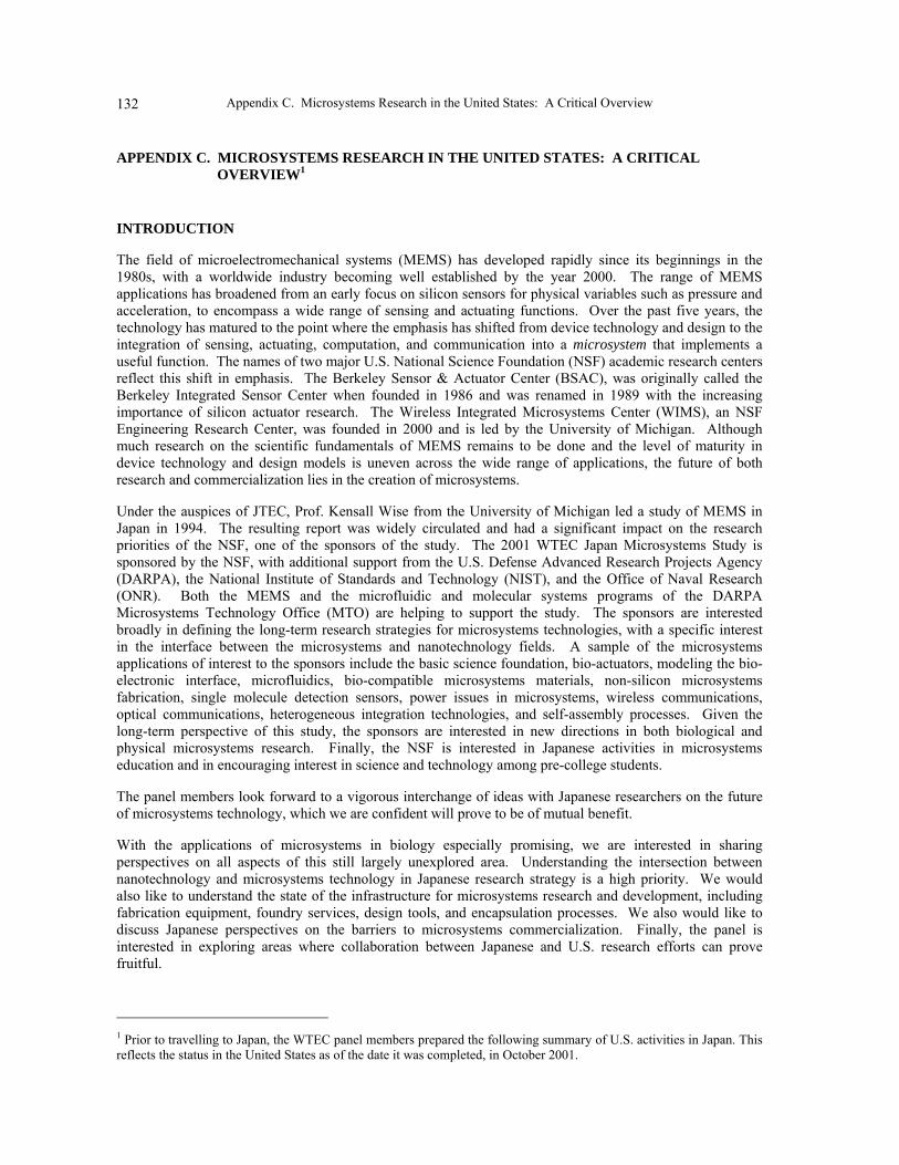
Radio frequency mechanical resonators and filters have motivated research on fabricating structures with lateral actuating gaps that are 100 nm or smaller�beyond the state of the art in optical lithography and etching processes. One approach is to use sacrificial layers defined by sidewall spacers (Hsu 2001), as shown in Fig. C.1. This resonator is the first MEMS micromechanical device capable of operation at 150 MHz with a Q approaching 10,000. The polysilicon disk is patterned by optical lithography, after which a conformal oxide film is defined that will later be etched. The oxide layer provides electrical isolation for the plating base for a nickel drive electrode. Although the sidewall technique is limited in its application, it will play an important role in the precise definition of offsets in micro/nano structures.
µmechanical DiskResonator
MetalElectrode
MetalElectrode
R
Anchor
Figure C.1. SEM of a micromachined disc resonator with submicron gaps. This resonator is the first MEMS
device capable of operation at 150 MHz with a Q approaching 10,000.
Many emerging applications also require the definition of fine features (< 1 µm) on devices for RF MEMS, bio-MEMS, high-density interconnects, and nano-mechanical systems. Many groups are using many of the standard submicron lithography techniques such as electron beams. However, e-beam lithography is still mostly a research tool that may not find its way to production too easily. As the integrated circuit (IC) industry develops deep-UV based lithography technologies for submicron IC manufacturing, these technologies are being increasingly used by the MEMS community to produce MEMS at reasonable cost. Therefore, it is expected that for the foreseeable future MEMS will continue to ride the wave of shrinking features that the IC industry has generated.
Appendix C. Microsystems Research in the United States: A Critical Overview 134
It is worth noting that one technology, namely focused ion beam (FIB) etching and deposition, is finding increasing use in MEMS and NEMS. Focused ion beams have been used for a long time by some in the IC industry for diagnostics and testing. The MEMS community has recently started to use this technique since it provides the capability to etch and deposit various materials with small and well-defined dimensions in situ without the need for lithography.
Three-Dimensional Micromachining Processes
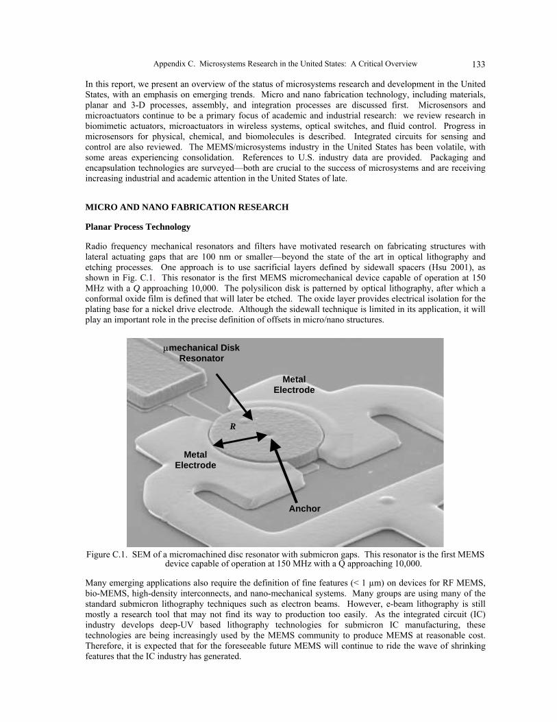
The trend in the United States has been for 3-D micromachining strategies to be rooted in the existing expertise and momentum of planar surface micromachining. An early example of this was hinged surface micromachined structures, which have now found a marketable application in optical switching (Fig. C.2(a)). Numerous techniques have been developed to actuate these structures out of plane without manual manipulation.
The surface micromachining process itself has been extended up to five levels of polysilicon in the commercially available Sandia SUMMiT-V process (Fig. C.2(b)).
(a) (b) (c)
Figure C.2. Examples of 3-D MEMS: (a) 8 x 8 switching array of digital micromirrors from Optical Micro Machines, Inc. (b) Complex 3-D integration of planar parts in the SUMMiT-V process from Sandia
National Labs. (c) The combustor and turbine elements of the MIT micro turbine engine.
More recently, Bosch deep-trench etching has dominated U.S. MEMS research. Although, most Bosch-etched structures have tended to be simply extruded versions of previous surface-micromachined designs, key advantages of the thicker designs are increased capacitance and mechanical rigidity. The latter benefit is particularly suitable for optical mirrors (Conant 2000). To achieve more truly 3-D structures from this technique, stacks of multiple wafers have been bonded. An extreme example of this is the MIT microturbine project (Figure C.2(c)), in which up to seven wafers are bonded at various stages of the process flow. Other techniques include multi-level Bosch etches in a single wafer, sometimes from both sides (Last et al. 2002), or serial assembly of Bosch-etched parts using mechanical interlocking connections (Zhou et al. 2002).
LIGA-like molding processes have seen comparatively less attention in the United States recently, in comparison to Bosch-etched silicon. Of note, however, is the great amount of attention given to molded polymers for biological microfluidics applications (Boone et al. 1998). Professor Stephen Quake at Caltech has achieved 3-D channel networks with integrated pumps and valves, using stacks of silicone elastomer simply molded off of photoresist (Unger et al.
In U.S. MEMS research, truly 3-D microstructures have not been the focus of much research, due to the reluctance of most research groups to pursue serial machining techniques or to utilize serial assembly. Momentum is beginning to build, however, in the use of batch assembly techniques, such as parallel transfer or stochastic self-assembly. Although the focus on batch processes could be viewed as restrictive, it may be argued that the resulting devices have been more amenable to low-cost mass production.
Appendix C. Microsystems Research in the United States: A Critical Overview 135
Parallel Assembly Processes
Through the 80s and early 90s, the United States favored a MEMS paradigm that emphasized batch processes and monolithic integration. From a manufacturing standpoint, it is very attractive to avoid serial assembly of system components, instead having all elements fabricated in place, as defined lithographically. However, the design space of systems that can be realized in such a manner is limited, particularly in the case of 3-D structures or the use of non-IC materials. In addition, a completely monolithic process may not be the most economically efficient. For example, one would not want to consume a large amount of die space in a high-performance CMOS process for use as a simple proof mass.
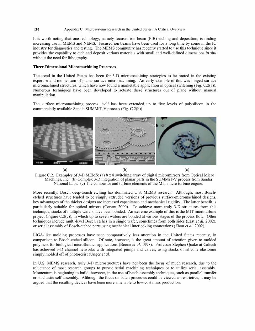
It is generally recognized that for many microsystems, some assembly is required. The desire for batch manufacturing remains, however; and so in recent years, there has been much U.S. research on parallel or self-assembly processes. Kris Pister showed that 3-D structures could be assembled from surface micromachined parts using hinges (Pister et al. 1992) (Fig. C.3(a)). The power of this technique to build complex structures is illustrated in the miniature model of the University of California, Berkeley, campanile clock tower (Hui et al. 2000) shown in Fig. C.3(b). This structure is a good example of design for assembly. The many elements, as fabricated, are arranged and constrained in such a manner that rotating a single element by 180° assembles the entire structure. Fold-up structures have been batch assembled, for example, using solder balls patterned on the structure (Kladitis et al. 2001) (Fig. C.3(c)) or with ultrasonic vibration (Kaajakari and Lal 2001) (Fig. C.3(d)).
(a) (b) (c) (d) Figure C.3. Examples of assembled 3-D structures: (a) first hinged plate, (b) micro-scale model of Berkeley
campanile clock tower, (c) reflowed solder balls used to self-assemble fan blades, and (d) batch assembly of fold-up mirrors by ultrasonic vibration.
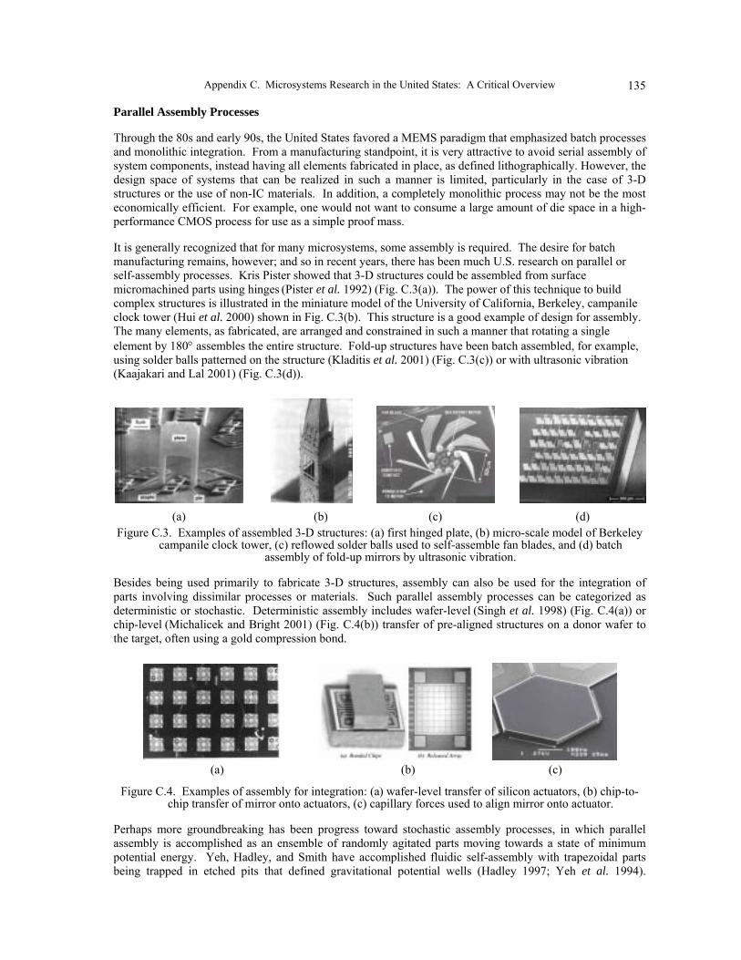
Besides being used primarily to fabricate 3-D structures, assembly can also be used for the integration of parts involving dissimilar processes or materials. Such parallel assembly processes can be categorized as deterministic or stochastic. Deterministic assembly includes wafer-level (Singh et al. 1998) (Fig. C.4(a)) or chip-level (Michalicek and Bright 2001) (Fig. C.4(b)) transfer of pre-aligned structures on a donor wafer to the target, often using a gold compression bond.
(a) (b) (c)
Figure C.4. Examples of assembly for integration: (a) wafer-level transfer of silicon actuators, (b) chip-to-chip transfer of mirror onto actuators, (c) capillary forces used to align mirror onto actuator.
Perhaps more groundbreaking has been progress toward stochastic assembly processes, in which parallel assembly is accomplished as an ensemble of randomly agitated parts moving towards a state of minimum potential energy. Yeh, Hadley, and Smith have accomplished fluidic self-assembly with trapezoidal parts being trapped in etched pits that defined gravitational potential wells (Hadley 1997; Yeh et al. 1994).
Appendix C. Microsystems Research in the United States: A Critical Overview 136
Through the patterning of self-assembled monolayers, potential wells from capillary forces have been applied for the assembly of bulk micromachined mirrors onto surface micromachined actuators (Srinivasan et al. 2000) (Fig. C.4(c)). In addition, stochastic assembly has been accomplished in a dry environment through the use of piezoelectric vibration, coupled with electrostatic potential wells (Bohringer et al. 1997), to break sticking forces.
MEMS/CMOS Integration Strategies
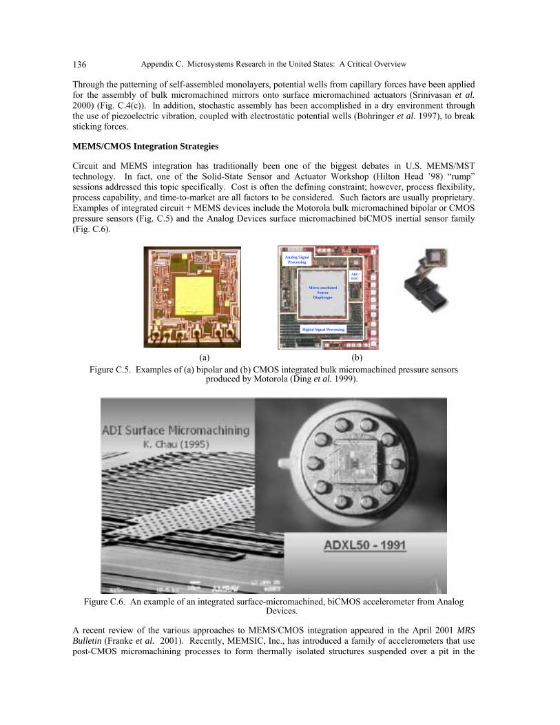
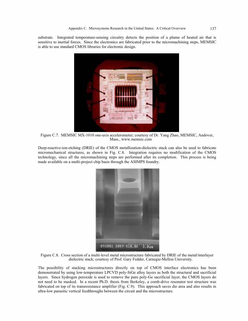
Circuit and MEMS integration has traditionally been one of the biggest debates in U.S. MEMS/MST technology. In fact, one of the Solid-State Sensor and Actuator Workshop (Hilton Head �98) �rump� sessions addressed this topic specifically. Cost is often the defining constraint; however, process flexibility, process capability, and time-to-market are all factors to be considered. Such factors are usually proprietary. Examples of integrated circuit + MEMS devices include the Motorola bulk micromachined bipolar or CMOS pressure sensors (Fig. C.5) and the Analog Devices surface micromachined biCMOS inertial sensor family (Fig. C.6).
Micro-machinedSensor
Diaphragm
Analog SignalProcessing
ADC/DAC
Digital Signal Processing
(a) (b)
Figure C.5. Examples of (a) bipolar and (b) CMOS integrated bulk micromachined pressure sensors produced by Motorola (Ding et al. 1999).
Figure C.6. An example of an integrated surface-micromachined, biCMOS accelerometer from Analog
Devices.
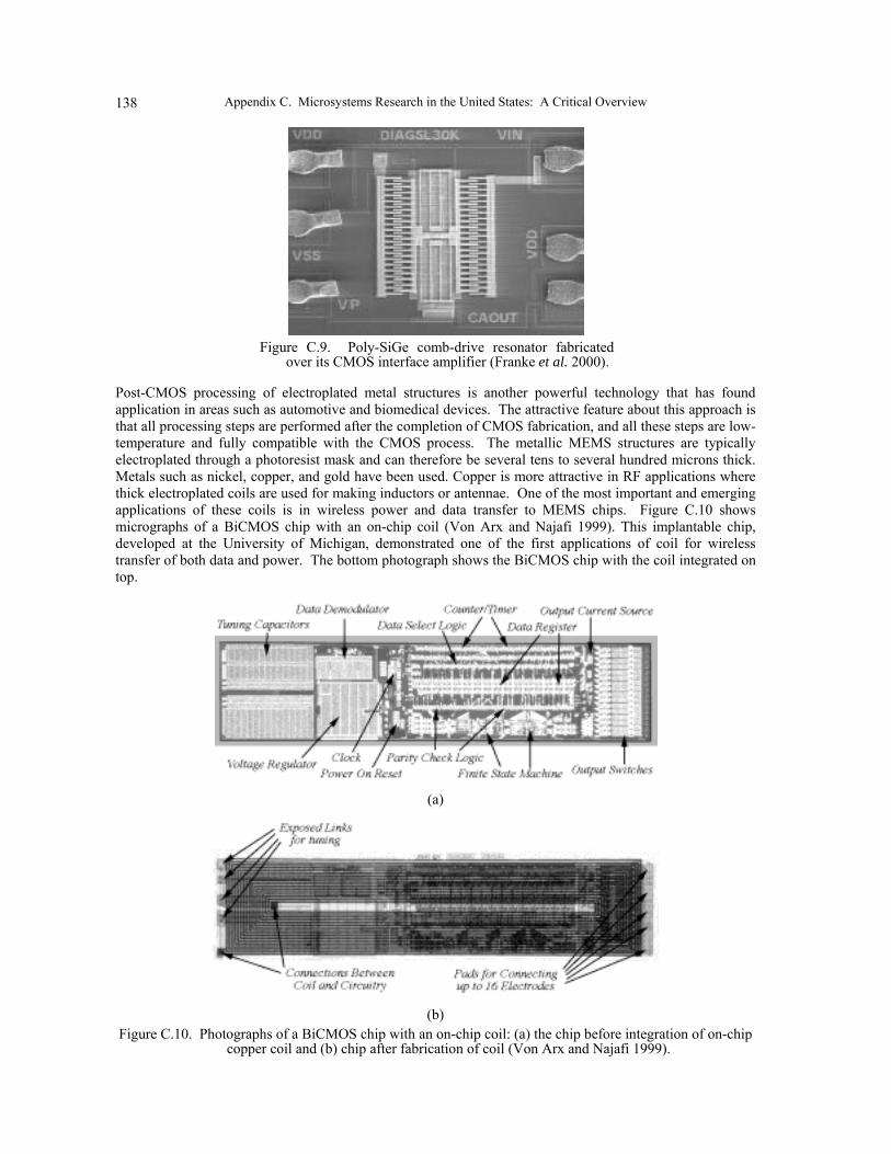
A recent review of the various approaches to MEMS/CMOS integration appeared in the April 2001 MRS Bulletin (Franke et al. 2001). Recently, MEMSIC, Inc., has introduced a family of accelerometers that use post-CMOS micromachining processes to form thermally isolated structures suspended over a pit in the
Appendix C. Microsystems Research in the United States: A Critical Overview 137
substrate. Integrated temperature-sensing circuitry detects the position of a plume of heated air that is sensitive to inertial forces. Since the electronics are fabricated prior to the micromachining steps, MEMSIC is able to use standard CMOS libraries for electronic design.
Figure C.7. MEMSIC MX-1010 one-axis accelerometer; courtesy of Dr. Yang Zhao, MEMSIC, Andover,
Mass., www.memsic.com
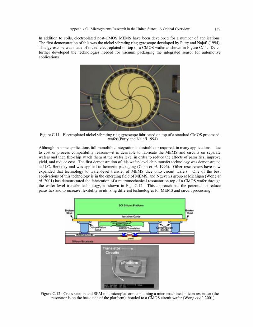
Deep-reactive-ion-etching (DRIE) of the CMOS metallization-dielectric stack can also be used to fabricate micromechanical structures, as shown in Fig. C.8. Integration requires no modification of the CMOS technology, since all the micromachining steps are performed after its completion. This process is being made available on a multi-project chip basis through the ASIMPS foundry.
Figure C.8. Cross section of a multi-level metal microstructure fabricated by DRIE of the metal/interlayer
dielectric stack; courtesy of Prof. Gary Fedder, Carnegie-Mellon University.
The possibility of stacking microstructures directly on top of CMOS interface electronics has been demonstrated by using low-temperature LPCVD poly-SiGe alloy layers as both the structural and sacrificial layers. Since hydrogen peroxide is used to remove the pure poly-Ge sacrificial layer, the CMOS layers do not need to be masked. In a recent Ph.D. thesis from Berkeley, a comb-drive resonator test structure was fabricated on top of its transresistance amplifier (Fig. C.9). This approach saves die area and also results in ultra-low parasitic vertical feedthroughs between the circuit and the microstructure.
Appendix C. Microsystems Research in the United States: A Critical Overview 138
Figure C.9. Poly-SiGe comb-drive resonator fabricated
over its CMOS interface amplifier (Franke et al. 2000).
Post-CMOS processing of electroplated metal structures is another powerful technology that has found application in areas such as automotive and biomedical devices. The attractive feature about this approach is that all processing steps are performed after the completion of CMOS fabrication, and all these steps are low-temperature and fully compatible with the CMOS process. The metallic MEMS structures are typically electroplated through a photoresist mask and can therefore be several tens to several hundred microns thick. Metals such as nickel, copper, and gold have been used. Copper is more attractive in RF applications where thick electroplated coils are used for making inductors or antennae. One of the most important and emerging applications of these coils is in wireless power and data transfer to MEMS chips. Figure C.10 shows micrographs of a BiCMOS chip with an on-chip coil (Von Arx and Najafi 1999). This implantable chip, developed at the University of Michigan, demonstrated one of the first applications of coil for wireless transfer of both data and power. The bottom photograph shows the BiCMOS chip with the coil integrated on top.
(a)
(b)
Figure C.10. Photographs of a BiCMOS chip with an on-chip coil: (a) the chip before integration of on-chip copper coil and (b) chip after fabrication of coil (Von Arx and Najafi 1999).
Appendix C. Microsystems Research in the United States: A Critical Overview 139
In addition to coils, electroplated post-CMOS MEMS have been developed for a number of applications. The first demonstration of this was the nickel vibrating ring gyroscope developed by Putty and Najafi (1994). This gyroscope was made of nickel electroplated on top of a CMOS wafer as shown in Figure C.11. Delco further developed the technologies needed for vacuum packaging the integrated sensor for automotive applications.
Figure C.11. Electroplated nickel vibrating ring gyroscope fabricated on top of a standard CMOS processed
wafer (Putty and Najafi 1994).
Although in some applications full monolithic integration is desirable or required, in many applications�due to cost or process compatibility reasons�it is desirable to fabricate the MEMS and circuits on separate wafers and then flip-chip attach them at the wafer level in order to reduce the effects of parasitics, improve yield, and reduce cost. The first demonstration of this wafer-level chip transfer technology was demonstrated at U.C. Berkeley and was applied to hermetic packaging (Cohn et al. 1996). Other researchers have now expanded that technology to wafer-level transfer of MEMS dice onto circuit wafers. One of the best applications of this technology is in the emerging field of MEMS, and Nguyen's group at Michigan (Wong et al. 2001) has demonstrated the fabrication of a micromechanical resonator on top of a CMOS wafer through the wafer level transfer technology, as shown in Fig. C.12. This approach has the potential to reduce parasitics and to increase flexibility in utilizing different technologies for MEMS and circuit processing.
Figure C.12. Cross section and SEM of a microplatform containing a micromachined silicon resonator (the
resonator is on the back side of the platform), bonded to a CMOS circuit wafer (Wong et al. 2001).
Appendix C. Microsystems Research in the United States: A Critical Overview 140
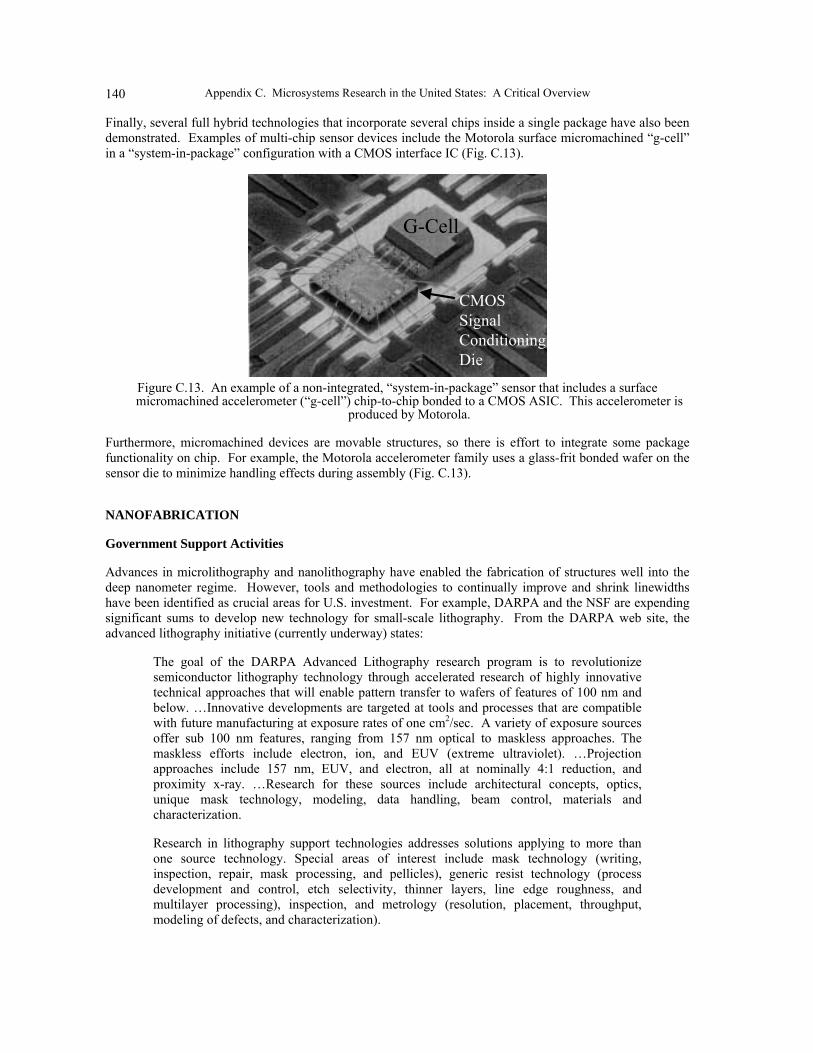
Finally, several full hybrid technologies that incorporate several chips inside a single package have also been demonstrated. Examples of multi-chip sensor devices include the Motorola surface micromachined �g-cell� in a �system-in-package� configuration with a CMOS interface IC (Fig. C.13).
G-Cell
CMOSSignal ConditioningDie
Figure C.13. An example of a non-integrated, �system-in-package� sensor that includes a surface micromachined accelerometer (�g-cell�) chip-to-chip bonded to a CMOS ASIC. This accelerometer is
produced by Motorola.
Furthermore, micromachined devices are movable structures, so there is effort to integrate some package functionality on chip. For example, the Motorola accelerometer family uses a glass-frit bonded wafer on the sensor die to minimize handling effects during assembly (Fig. C.13).
NANOFABRICATION
Government Support Activities
Advances in microlithography and nanolithography have enabled the fabrication of structures well into the deep nanometer regime. However, tools and methodologies to continually improve and shrink linewidths have been identified as crucial areas for U.S. investment. For example, DARPA and the NSF are expending significant sums to develop new technology for small-scale lithography. From the DARPA web site, the advanced lithography initiative (currently underway) states:
The goal of the DARPA Advanced Lithography research program is to revolutionize semiconductor lithography technology through accelerated research of highly innovative technical approaches that will enable pattern transfer to wafers of features of 100 nm and below. �Innovative developments are targeted at tools and processes that are compatible with future manufacturing at exposure rates of one cm2/sec. A variety of exposure sources offer sub 100 nm features, ranging from 157 nm optical to maskless approaches. The maskless efforts include electron, ion, and EUV (extreme ultraviolet). �Projection approaches include 157 nm, EUV, and electron, all at nominally 4:1 reduction, and proximity x-ray. �Research for these sources include architectural concepts, optics, unique mask technology, modeling, data handling, beam control, materials and characterization.
Research in lithography support technologies addresses solutions applying to more than one source technology. Special areas of interest include mask technology (writing, inspection, repair, mask processing, and pellicles), generic resist technology (process development and control, etch selectivity, thinner layers, line edge roughness, and multilayer processing), inspection, and metrology (resolution, placement, throughput, modeling of defects, and characterization).
Appendix C. Microsystems Research in the United States: A Critical Overview 141
Research in nanolithography technology addresses emerging devices, structures, and circuit functions that exploit features down to 10 nm and below. This includes tools or subsystems for patterning, materials, processing, 3-D device patterning, mask technology, modeling, characterization, and device demonstrations.
Additional investments into infrastructure include the U.S. National Nanofabrication Facility (NNUF), funded in large part by the NSF. The facility operates as a distributed user facility, with a distributed National Nanofabrication Users Network (NNUN), which can give users access to sophisticated nanofabrication technologies, without each user needing to acquire the capital-cost-intensive equipment that would otherwise be required to perform experimental research in this area. The NNUN is open to all users from academia, government, and industry. More from the NNUN:
The combined staffs of the NNUN have extensive experience in all phases of nanofabrication and its use in fields ranging from nanophysics to biology to electronics. We have �domain experts� in micromechanics and biology to assist users in translating their ideas into experimental reality. With the assistance of the NNUN, users can often fabricate advanced nanostructures within weeks of initial contact. The NNUN also provides outreach support to the community through its Research Experience for Undergraduates program and training workshops. Our technologies are largely based on the thin film patterning techniques so successfully employed in the microelectronics industry. Extensive development and characterization within NNUN allows us to apply these same fabrication techniques to a wide range of materials and to diverse areas of science and technology. By working with NNUN, users gain access to extensive modern equipment and staff support.
In addition to the NNUN, the NSF is sponsoring a variety of programs to develop nanotechnology. The goal of these programs is as follows:
to support fundamental research and catalyze synergistic science and engineering research and education in emerging areas of nanoscale science and technology, including biosystems at the nanoscale; nanoscale structures, novel phenomena, and quantum control; device and system architecture; design tools and nanosystems specific software; nanoscale processes in the environment; multi-scale, multi-phenomena modeling and simulation at the nanoscale; manufacturing processes at the nanoscale; and studies on the societal implications of nanoscale science and engineering.
In particular, there is currently a competition for �NIRTs� and �NERs�. Nanoscale Interdisciplinary Research Teams (NIRTs) are teams of 3-5 people from various disciplines to work together for 3-5 years on an interdisciplinary nanotechnology project. Nanoscale Exploratory Research (NERs) are typically one-year, one- or two-investigator seed programs, that allow the investigation of new nanoscale phenomena prior to investment in a full research program.
The U.S. Army Research Office (ARO) is planning substantial funding in the area of nanofabrication through the Center of Research for Nanoscience for the Soldier. This program is currently in the stages of inviting proposals to be submitted, with awards to be announced at the end of 2002. The purpose is to create a
University Affiliated Research Center (UARC) to develop nanometer-scale science and technology solutions for the soldier. A single university, along with industry partners, will host this center to emphasize revolutionary materials research toward an advanced uniform and protective ensemble concept. <�> Through this competition, the ARO expects to award a single non-fee-bearing contract having an initial performance period of five years and an estimated base cost of $50,000,000. <�> The resulting contract will include provisions for task orders for additional effort estimated to reach $20,000,000 over the five-year term.
In addition to tool and infrastructure development programs, the government is also funding application-driven research. As just one example of many, DARPA is currently funding a program on �Nano-
Appendix C. Microsystems Research in the United States: A Critical Overview 142
Mechanical Array Signal Processors� (NMASP). The goal of this program is to demonstrate arrays of nano-precision high-Quality-factor (Q on the order of 10,000) ultra-high frequency (UHF) (300 MHz to 3 GHz) mechanical resonators that will achieve radical reductions in size and power consumption over state-of-the-art RF transceivers and signal processors.
Research
Research in this area can loosely be divided into two approaches: the top-down approach, in which conventional MEMS techniques are extended into smaller and smaller realms, and the bottom-up approach, in which chemistry and self-assembly are utilized to fabricate microstructures. Although an exhaustive listing of the research programs being pursued are beyond the scope of this document, some highlights from both the top-down and bottom-up approaches are given below.
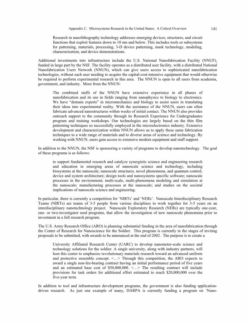
Top-down approaches are being pursued by a variety of researchers, including most notably Roukes at the California Institute of Technology and Craighead at Harvard University. Roukes has pioneered this area with nanoresonators (Fig. C.14(a)) and thermal quantization devices (Fig. C.14(b)).
(a) (b) Figure C.14. Nanostructure devices by Roukes at Caltech: (a) nanoresonator; (b) thermal quantization device
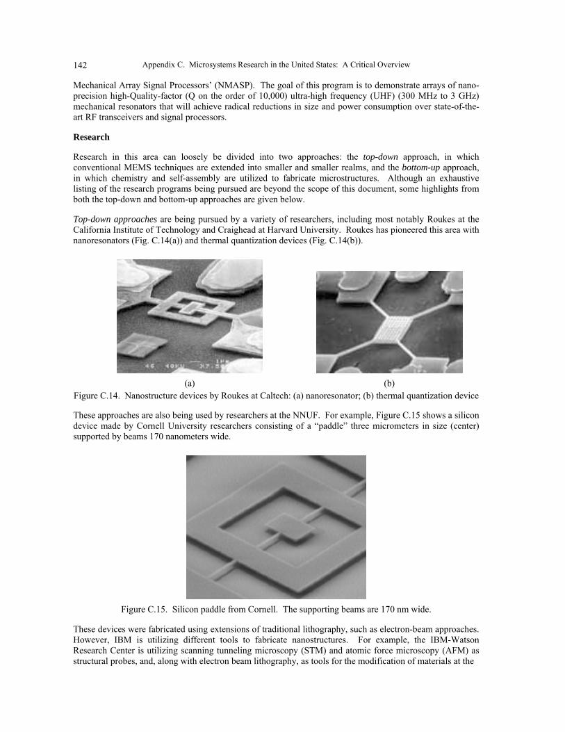
These approaches are also being used by researchers at the NNUF. For example, Figure C.15 shows a silicon device made by Cornell University researchers consisting of a �paddle� three micrometers in size (center) supported by beams 170 nanometers wide.
Figure C.15. Silicon paddle from Cornell. The supporting beams are 170 nm wide.
These devices were fabricated using extensions of traditional lithography, such as electron-beam approaches. However, IBM is utilizing different tools to fabricate nanostructures. For example, the IBM-Watson Research Center is utilizing scanning tunneling microscopy (STM) and atomic force microscopy (AFM) as structural probes, and, along with electron beam lithography, as tools for the modification of materials at the
Appendix C. Microsystems Research in the United States: A Critical Overview 143
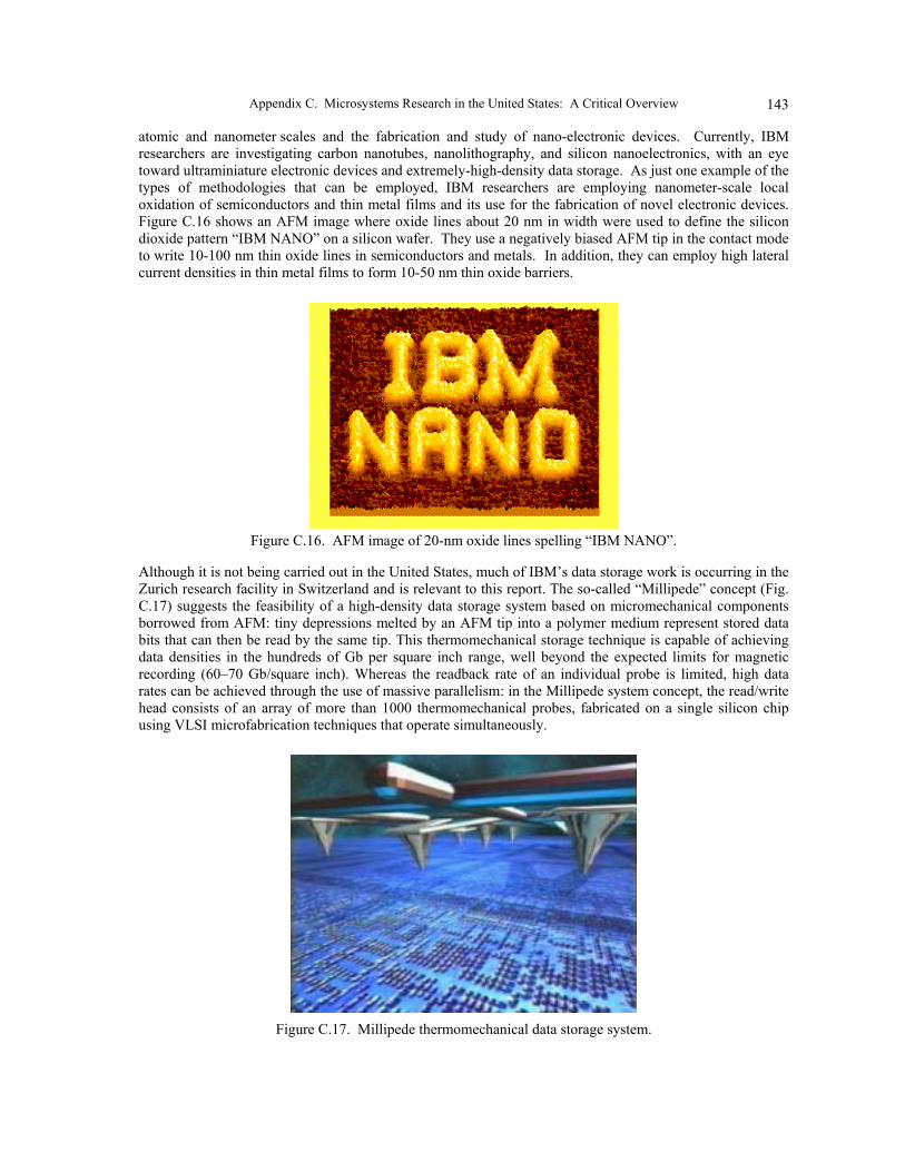
atomic and nanometer scales and the fabrication and study of nano-electronic devices. Currently, IBM researchers are investigating carbon nanotubes, nanolithography, and silicon nanoelectronics, with an eye toward ultraminiature electronic devices and extremely-high-density data storage. As just one example of the types of methodologies that can be employed, IBM researchers are employing nanometer-scale local oxidation of semiconductors and thin metal films and its use for the fabrication of novel electronic devices. Figure C.16 shows an AFM image where oxide lines about 20 nm in width were used to define the silicon dioxide pattern �IBM NANO� on a silicon wafer. They use a negatively biased AFM tip in the contact mode to write 10-100 nm thin oxide lines in semiconductors and metals. In addition, they can employ high lateral current densities in thin metal films to form 10-50 nm thin oxide barriers.
Figure C.16. AFM image of 20-nm oxide lines spelling �IBM NANO�.
Although it is not being carried out in the United States, much of IBM�s data storage work is occurring in the Zurich research facility in Switzerland and is relevant to this report. The so-called �Millipede� concept (Fig. C.17) suggests the feasibility of a high-density data storage system based on micromechanical components borrowed from AFM: tiny depressions melted by an AFM tip into a polymer medium represent stored data bits that can then be read by the same tip. This thermomechanical storage technique is capable of achieving data densities in the hundreds of Gb per square inch range, well beyond the expected limits for magnetic recording (60�70 Gb/square inch). Whereas the readback rate of an individual probe is limited, high data rates can be achieved through the use of massive parallelism: in the Millipede system concept, the read/write head consists of an array of more than 1000 thermomechanical probes, fabricated on a single silicon chip using VLSI microfabrication techniques that operate simultaneously.
Figure C.17. Millipede thermomechanical data storage system.
Appendix C. Microsystems Research in the United States: A Critical Overview 144
Bottom-Up Approaches are primarily being undertaken from the realm of chemistry. Lithography is typically used to define chemically-active regions on a surface, followed by sequential immersion in appropriate chemical solutions to grow self-assembled monolayers on the patterned surfaces. Both traditional lithography (including that used to manufacture structures as shown in the previous section) as well as so-called �soft lithography� can be used prior to self-assembly.
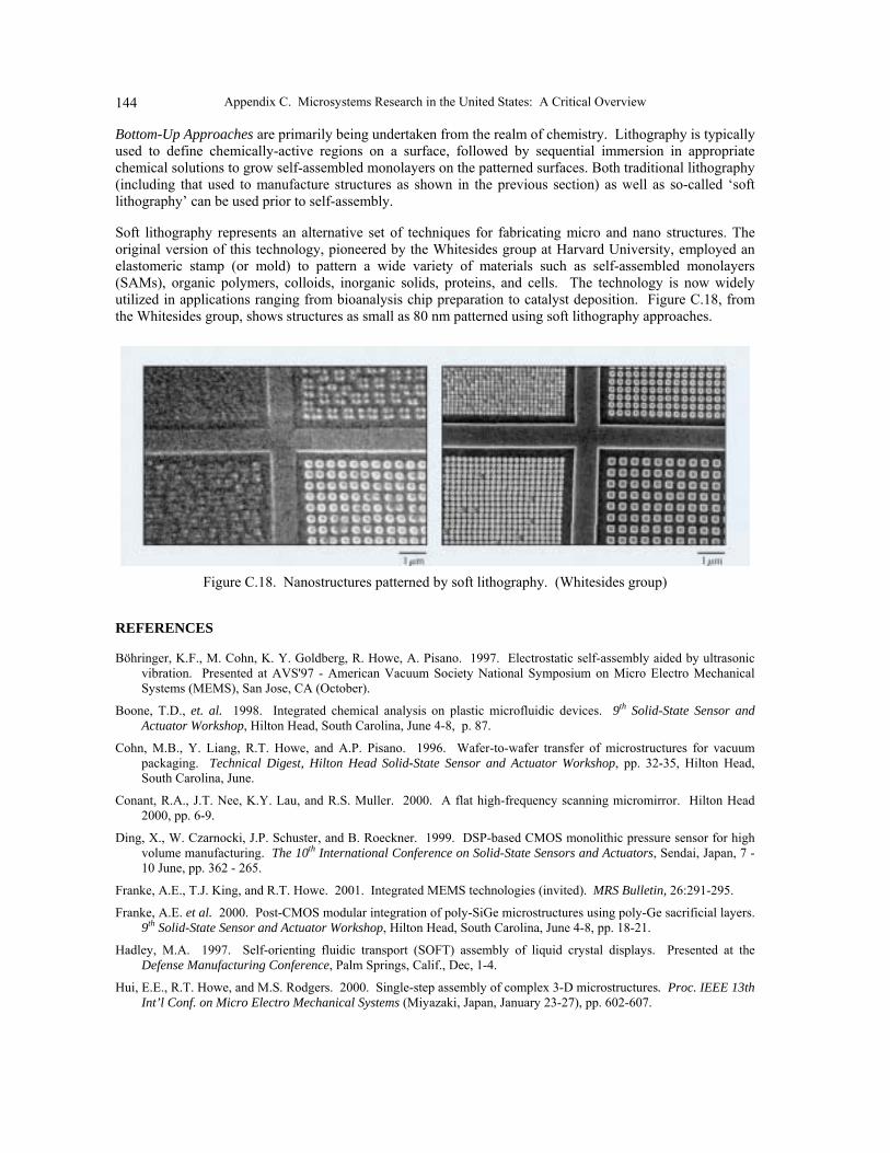
Soft lithography represents an alternative set of techniques for fabricating micro and nano structures. The original version of this technology, pioneered by the Whitesides group at Harvard University, employed an elastomeric stamp (or mold) to pattern a wide variety of materials such as self-assembled monolayers (SAMs), organic polymers, colloids, inorganic solids, proteins, and cells. The technology is now widely utilized in applications ranging from bioanalysis chip preparation to catalyst deposition. Figure C.18, from the Whitesides group, shows structures as small as 80 nm patterned using soft lithography approaches.
Figure C.18. Nanostructures patterned by soft lithography. (Whitesides group)
REFERENCES
Böhringer, K.F., M. Cohn, K. Y. Goldberg, R. Howe, A. Pisano. 1997. Electrostatic self-assembly aided by ultrasonic vibration. Presented at AVS'97 - American Vacuum Society National Symposium on Micro Electro Mechanical Systems (MEMS), San Jose, CA (October).
Boone, T.D., et. al. 1998. Integrated chemical analysis on plastic microfluidic devices. 9th Solid-State Sensor and Actuator Workshop, Hilton Head, South Carolina, June 4-8, p. 87.
Cohn, M.B., Y. Liang, R.T. Howe, and A.P. Pisano. 1996. Wafer-to-wafer transfer of microstructures for vacuum packaging. Technical Digest, Hilton Head Solid-State Sensor and Actuator Workshop, pp. 32-35, Hilton Head, South Carolina, June.
Conant, R.A., J.T. Nee, K.Y. Lau, and R.S. Muller. 2000. A flat high-frequency scanning micromirror. Hilton Head 2000, pp. 6-9.
Ding, X., W. Czarnocki, J.P. Schuster, and B. Roeckner. 1999. DSP-based CMOS monolithic pressure sensor for high volume manufacturing. The 10th International Conference on Solid-State Sensors and Actuators, Sendai, Japan, 7 - 10 June, pp. 362 - 265.
Franke, A.E., T.J. King, and R.T. Howe. 2001. Integrated MEMS technologies (invited). MRS Bulletin, 26:291-295.
Franke, A.E. et al. 2000. Post-CMOS modular integration of poly-SiGe microstructures using poly-Ge sacrificial layers. 9th Solid-State Sensor and Actuator Workshop, Hilton Head, South Carolina, June 4-8, pp. 18-21.
Hadley, M.A. 1997. Self-orienting fluidic transport (SOFT) assembly of liquid crystal displays. Presented at the Defense Manufacturing Conference, Palm Springs, Calif., Dec, 1-4.
Hui, E.E., R.T. Howe, and M.S. Rodgers. 2000. Single-step assembly of complex 3-D microstructures. Proc. IEEE 13th Int’l Conf. on Micro Electro Mechanical Systems (Miyazaki, Japan, January 23-27), pp. 602-607.
Appendix C. Microsystems Research in the United States: A Critical Overview 145
Hsu, W.T., J.R. Clark, and C.T.C. Nguyen. 2001. A sub-micron capacitive gap process for multiple-metal-electrode lateral micromechanical resonators. 14th Int. IEEE Micro Electro Mechanical Systems Conference, Interlaken, Switzerland, Jan. 21-25.
Kaajakari, V., and A. Lal. 2001. Electrostatic batch assembly of surface MEMS using ultrasonic triboelectricity. MEMS �01, pp. 10-13.
Kladitis, P.E., R.J. Linderman, and V.M. Bright. 2001. Solder self-assembled micro axial flow fan driven by a scratch drive actuator rotary motor. MEMS �01, pp. 598-601.
Last, M., et. al. 2002. To be presented at MEMS 2002 in Las Vegas, Nevada.
Michalicek, M.A., and V. M. Bright. 2001. Flip-chip fabrication of advanced micromirror arrays. MEMS �01, pp. 313-316.
Pister, K.J.S., et. al. 1992. Sensors and Actuators A, 33:249-25.
Putty, M.W., and K. Najafi. 1994. A micromachined vibrating ring gyroscope (invited paper). Technical Digest, Solid-State Sensors and Actuators Workshop, Hilton Head, SC, June, pp. 213-220,
Singh, A., D.A. Horsley, M.B. Cohn, A.P. Pisano, R.T. Howe. 1998. Batch transfer of microstructures using flip-chip solder bonding. Journal of Microelectromechanical Systems submitted 5/98.
Srinivasan, U., M.H. Helmbrecht, C. Rembe, R.S. Muller, and R.T. Howe. 2000. Fluidic self-assembly of micromirrors onto surface micromachined actuators. Proc. 2000 IEEE/LEOS Intl. Conf. on Optical MEMS, Kauai, HI, USA, Aug. 21-4, pp. 59-60.
Unger, M.A., H.P. Chou, T. Thorsen, A. Scherer, S.R. Quake. Monolithic microfabricated valves and pumps by multilayer soft lithography. Science 288: 113-116.
Von Arx, J.A., and K. Najafi. 1999. A single chip fully-integrated telemetry-powered system for peripheral nerve stimulation. Digest, IEEE Int. Conf. On Solid-State Circuits (ISSCC ‘99), pp. 214-215, San Francisco, February.
Wong, A.C., Y. Xie, and C.T.C. Nguyen. 2001. A bonded micro-platform technology for modular merging of RF MEMS and transistors. Digest, Int. Conf. On Solid-State Sensors and Actuators, Transducers 2001, Munich, Germany, June, pp. 992-995.
Yeh, H.J., and J.S. Smith. 1994. Fluidic self-assembly of microstructures and its application to the integration of GaAs on Si. Proceedings IEEE Micro Electro Mechanical Systems, Oiso, Japan, 25-28 Jan 1994 / New York: IEEE, 1994, pp.279-84.
Zhou, L., et. al. to be presented at MEMS 2002 in Las Vegas, Nevada
MICROSENSORS AND MICROACTUATORS
The authors wish to thank S. Sibbett and M. Dierks for contributions to this section
MEMS Transduction Mechanisms
MEMS activities in the United States for the most part have evolved from a background of semiconductor wafer processing, but have broadened over time to include meso-scale devices and non-silicon fabrication techniques such as soft lithography and hot embossing.
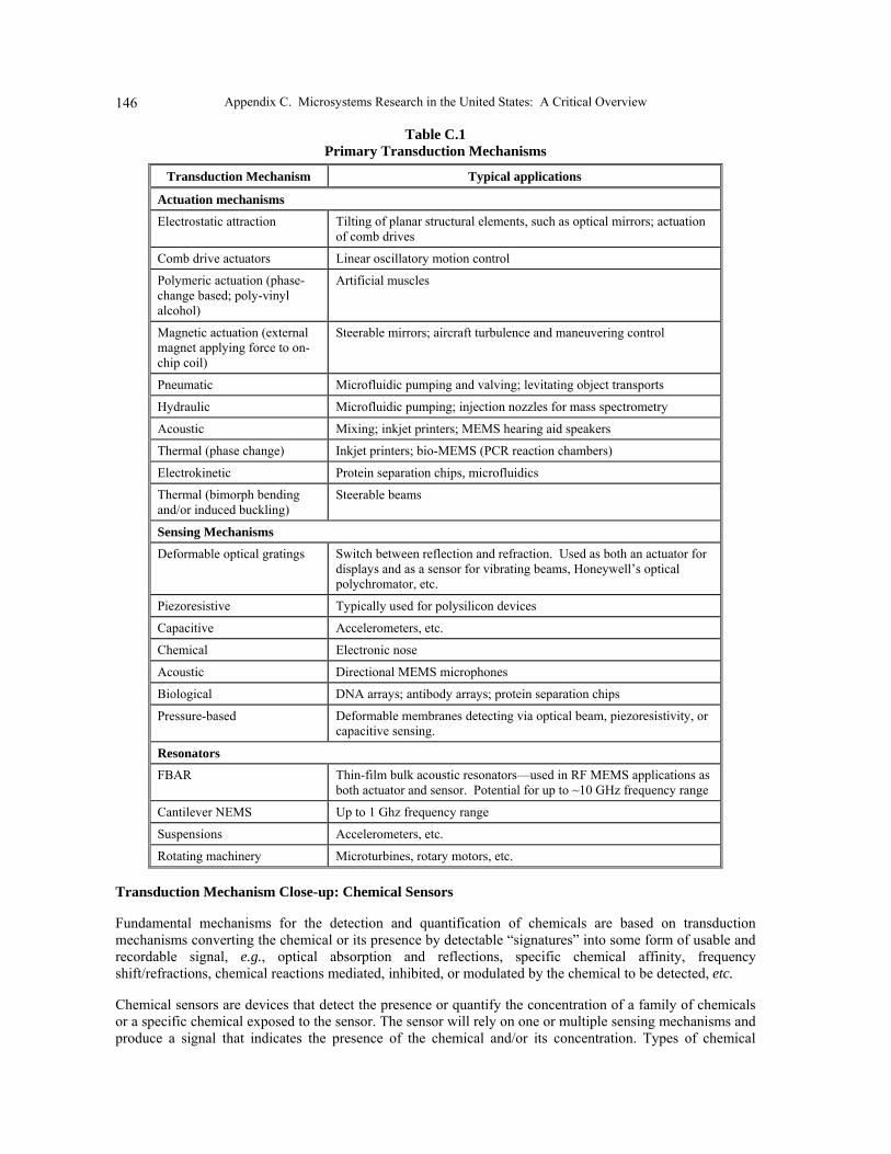
Some of the primary transduction mechanisms are listed in Table C.1
Appendix C. Microsystems Research in the United States: A Critical Overview 146
Table C.1 Primary Transduction Mechanisms
Transduction Mechanism Typical applications
Actuation mechanisms
Electrostatic attraction Tilting of planar structural elements, such as optical mirrors; actuation of comb drives
Comb drive actuators Linear oscillatory motion control
Polymeric actuation (phase-change based; poly-vinyl alcohol)
Artificial muscles
Magnetic actuation (external magnet applying force to on-chip coil)
Steerable mirrors; aircraft turbulence and maneuvering control
Pneumatic Microfluidic pumping and valving; levitating object transports
Hydraulic Microfluidic pumping; injection nozzles for mass spectrometry
Acoustic Mixing; inkjet printers; MEMS hearing aid speakers
Thermal (phase change) Inkjet printers; bio-MEMS (PCR reaction chambers)
Electrokinetic Protein separation chips, microfluidics
Thermal (bimorph bending and/or induced buckling)
Steerable beams
Sensing Mechanisms
Deformable optical gratings Switch between reflection and refraction. Used as both an actuator for displays and as a sensor for vibrating beams, Honeywell�s optical polychromator, etc.
Piezoresistive Typically used for polysilicon devices
Capacitive Accelerometers, etc.
Chemical Electronic nose
Acoustic Directional MEMS microphones
Biological DNA arrays; antibody arrays; protein separation chips
Pressure-based Deformable membranes detecting via optical beam, piezoresistivity, or capacitive sensing.
Resonators
FBAR Thin-film bulk acoustic resonators�used in RF MEMS applications as both actuator and sensor. Potential for up to ~10 GHz frequency range
Cantilever NEMS Up to 1 Ghz frequency range
Suspensions Accelerometers, etc.
Rotating machinery Microturbines, rotary motors, etc.
Transduction Mechanism Close-up: Chemical Sensors
Fundamental mechanisms for the detection and quantification of chemicals are based on transduction mechanisms converting the chemical or its presence by detectable �signatures� into some form of usable and recordable signal, e.g., optical absorption and reflections, specific chemical affinity, frequency shift/refractions, chemical reactions mediated, inhibited, or modulated by the chemical to be detected, etc.
Chemical sensors are devices that detect the presence or quantify the concentration of a family of chemicals or a specific chemical exposed to the sensor. The sensor will rely on one or multiple sensing mechanisms and produce a signal that indicates the presence of the chemical and/or its concentration. Types of chemical
Appendix C. Microsystems Research in the United States: A Critical Overview 147
sensors include electrochemical sensors, gas sensors, mass sensors, thermal/calorimetric sensors, optical sensors, biosensors (detection raging from single biomolecules, multi-molecular compounds, components of organella or cells and tissues), etc. Different sensors operate in different phases of materials, e.g., vapor/gas, liquid, sol-gel, and solid, etc. for specific applications.
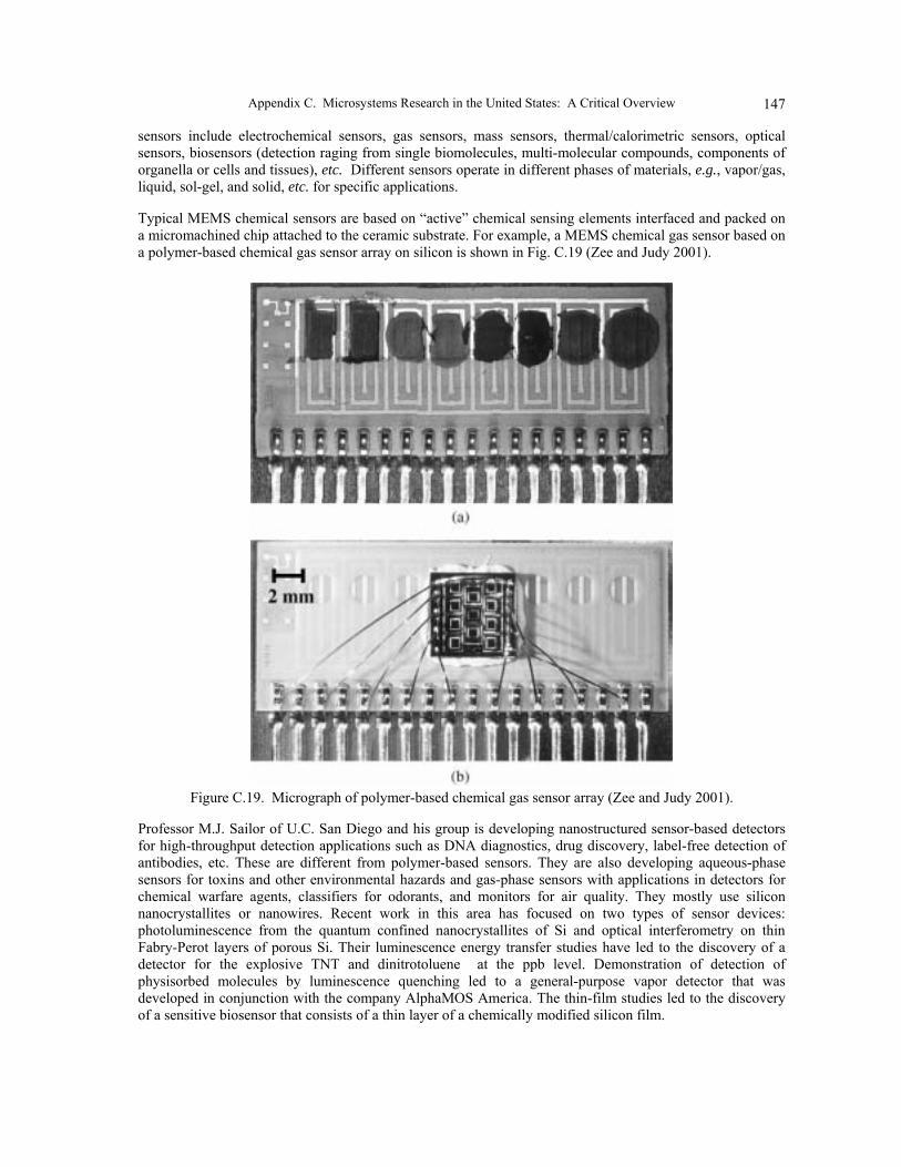
Typical MEMS chemical sensors are based on �active� chemical sensing elements interfaced and packed on a micromachined chip attached to the ceramic substrate. For example, a MEMS chemical gas sensor based on a polymer-based chemical gas sensor array on silicon is shown in Fig. C.19 (Zee and Judy 2001).
Figure C.19. Micrograph of polymer-based chemical gas sensor array (Zee and Judy 2001).
Professor M.J. Sailor of U.C. San Diego and his group is developing nanostructured sensor-based detectors for high-throughput detection applications such as DNA diagnostics, drug discovery, label-free detection of antibodies, etc. These are different from polymer-based sensors. They are also developing aqueous-phase sensors for toxins and other environmental hazards and gas-phase sensors with applications in detectors for chemical warfare agents, classifiers for odorants, and monitors for air quality. They mostly use silicon nanocrystallites or nanowires. Recent work in this area has focused on two types of sensor devices: photoluminescence from the quantum confined nanocrystallites of Si and optical interferometry on thin Fabry-Perot layers of porous Si. Their luminescence energy transfer studies have led to the discovery of a detector for the explosive TNT and dinitrotoluene at the ppb level. Demonstration of detection of physisorbed molecules by luminescence quenching led to a general-purpose vapor detector that was developed in conjunction with the company AlphaMOS America. The thin-film studies led to the discovery of a sensitive biosensor that consists of a thin layer of a chemically modified silicon film.
Appendix C. Microsystems Research in the United States: A Critical Overview 148
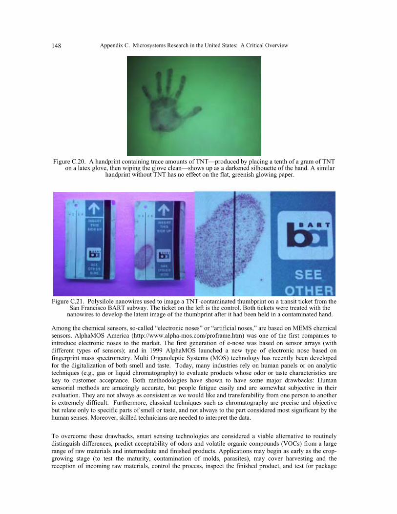
Figure C.20. A handprint containing trace amounts of TNT�produced by placing a tenth of a gram of TNT
on a latex glove, then wiping the glove clean�shows up as a darkened silhouette of the hand. A similar handprint without TNT has no effect on the flat, greenish glowing paper.
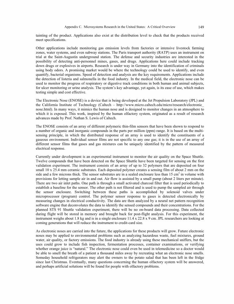
Figure C.21. Polysilole nanowires used to image a TNT-contaminated thumbprint on a transit ticket from the
San Francisco BART subway. The ticket on the left is the control. Both tickets were treated with the nanowires to develop the latent image of the thumbprint after it had been held in a contaminated hand.
Among the chemical sensors, so-called �electronic noses� or �artificial noses,� are based on MEMS chemical sensors. AlphaMOS America (http://www.alpha-mos.com/proframe.htm) was one of the first companies to introduce electronic noses to the market. The first generation of e-nose was based on sensor arrays (with different types of sensors); and in 1999 AlphaMOS launched a new type of electronic nose based on fingerprint mass spectrometry. Multi Organoleptic Systems (MOS) technology has recently been developed for the digitalization of both smell and taste. Today, many industries rely on human panels or on analytic techniques (e.g., gas or liquid chromatography) to evaluate products whose odor or taste characteristics are key to customer acceptance. Both methodologies have shown to have some major drawbacks: Human sensorial methods are amazingly accurate, but people fatigue easily and are somewhat subjective in their evaluation. They are not always as consistent as we would like and transferability from one person to another is extremely difficult. Furthermore, classical techniques such as chromatography are precise and objective but relate only to specific parts of smell or taste, and not always to the part considered most significant by the human senses. Moreover, skilled technicians are needed to interpret the data.
To overcome these drawbacks, smart sensing technologies are considered a viable alternative to routinely distinguish differences, predict acceptability of odors and volatile organic compounds (VOCs) from a large range of raw materials and intermediate and finished products. Applications may begin as early as the crop-growing stage (to test the maturity, contamination of molds, parasites), may cover harvesting and the reception of incoming raw materials, control the process, inspect the finished product, and test for package
Appendix C. Microsystems Research in the United States: A Critical Overview 149
tainting of the product. Applications also exist at the distribution level to check that the products received meet specifications.
Other applications include monitoring gas emission levels from factories or intensive livestock farming zones, water systems, and even subway stations. The Paris transport authority (RATP) uses an instrument on trial at the Saint-Augustin underground station. The defense and security industries are interested in the possibility of detecting anti-personnel mines, gases, and drugs. Applications here could include tracking down drugs or explosives in airports. Research is under way in Germany into the identification of criminals using body odors. A promising market would be where the technology could be used to identify, and even quantify, bacterial organisms. Speed of detection and analysis are the key requirements. Applications include the detection of listeria and salmonella in the food industry. In the medical field, the electronic nose can be used to monitor the progress of respiratory or digestive track conditions in both human and animal subjects, for ulcer monitoring or urine analysis. The system�s key advantage, yet again, is its ease of use, which makes testing simple and cost effective.
The Electronic Nose (ENOSE) is a device that is being developed at the Jet Propulsion Laboratory (JPL) and the California Institute of Technology (Caltech � http://www.micro.caltech.edu/micro/research/electronic_ nose.html). In many ways, it mimics the human nose and is designed to monitor changes in an atmosphere to which it is exposed. This work, inspired by the human olfactory system, originated as a result of research advances made by Prof. Nathan S. Lewis of Caltech.
The ENOSE consists of an array of different polymeric thin-film sensors that have been shown to respond to a number of organic and inorganic compounds in the parts per million (ppm) range. It is based on the multi-sensing principle, in which the distributed response of an array is used to identify the constituents of a gaseous environment. Individual sensor films are not specific to any one gas; it is in the use of an array of different sensor films that gases and gas mixtures can be uniquely identified by the pattern of measured electrical response.
Currently under development is an experimental instrument to monitor the air quality on the Space Shuttle. Twelve compounds that have been detected on the Space Shuttle have been targeted for sensing on the first validation experiment. The instrument consists of an array of up to 32 polymers that are deposited on four small 10 x 25.4 mm ceramic substrates. Each deposited polymer creates a sensing film of about 2 mm on the side and a few microns thick. The sensor substrates are in a sealed enclosure less than 15 cm3 in volume with provisions for letting sample air in and out. Air flow is assisted by a small pump (about 2 liters per minute). There are two air inlet paths. One path is through a small activated charcoal filter that is used periodically to establish a baseline for the sensor. The other path is not filtered and is used to pump the sampled air through the sensor enclosure. Switching between these paths is accomplished by solenoid valves under microprocessor (program) control. The polymer sensor response to gases is detected electronically by measuring changes in electrical conductivity. The data are then analyzed by a neural net pattern recognition software engine that deconvolutes the data to identify the sensed compounds and their concentrations. For the planned STS 91 Shuttle validation experiment, there will be no on-board data processing. Data collected during flight will be stored in memory and brought back for post-flight analysis. For this experiment, the instrument weighs about 1.8 kg and is in a single enclosure 11.4 x 22.8 x 9 cm. JPL researchers are looking at coming generations that will reduce the instrument to credit-card size.
As electronic noses are carried into the future, the applications for these products will grow. Future electronic noses may be applied to environmental problems such as analyzing hazardous waste, fuel mixtures, ground water, air quality, or factory emissions. The food industry is already using these mechanical sniffers, but the uses could grow to include fish inspection, fermentation processes, container examinations, or verifying whether orange juice is �natural.� The electronic nose could even be used in telemedicine so a doctor would be able to smell the breath of a patient a thousand miles away by recreating what an electronic nose smells. Someday household refrigerators may alert the owners to the potato salad that has been left in the fridge since last Christmas. Eventually, many questions concerning the human olfactory system will be answered, and perhaps artificial solutions will be found for people with olfactory problems.
Appendix C. Microsystems Research in the United States: A Critical Overview 150
Interface Electronics
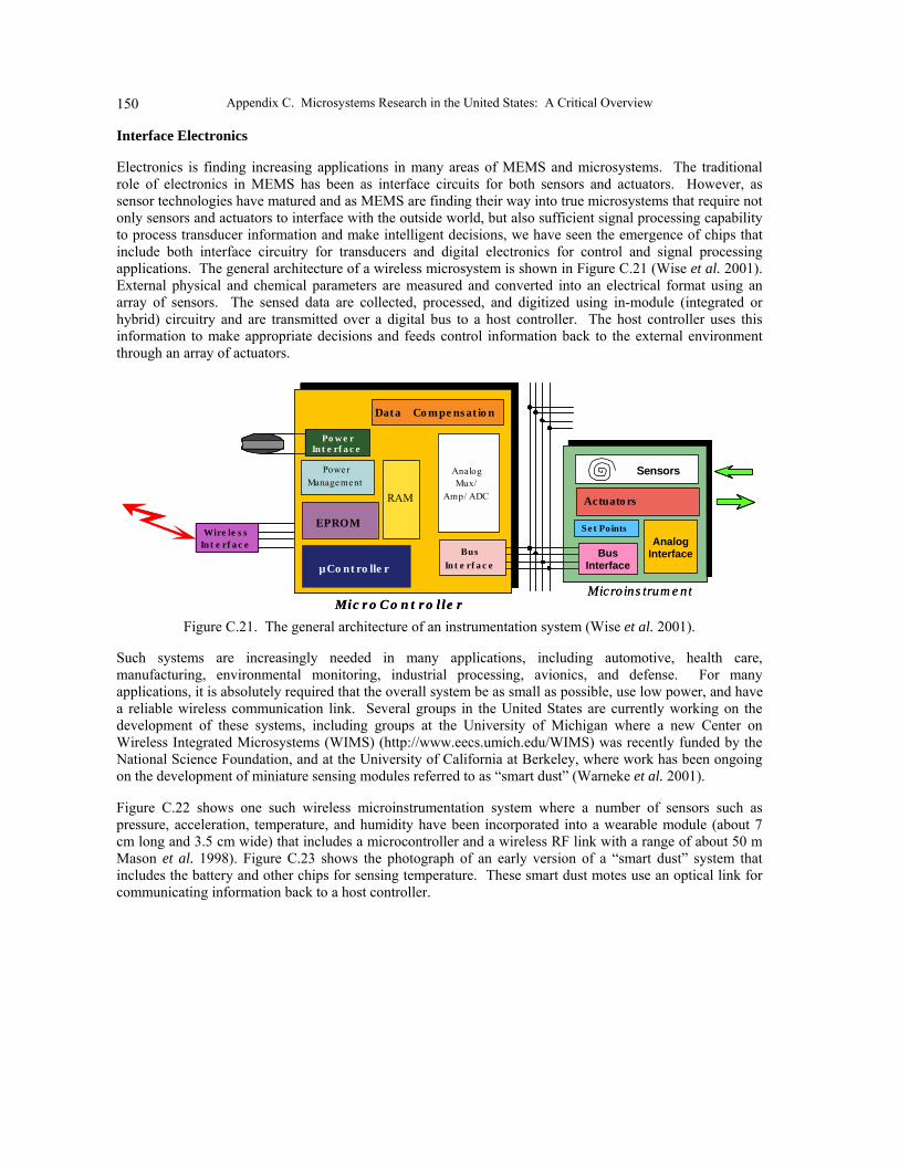
Electronics is finding increasing applications in many areas of MEMS and microsystems. The traditional role of electronics in MEMS has been as interface circuits for both sensors and actuators. However, as sensor technologies have matured and as MEMS are finding their way into true microsystems that require not only sensors and actuators to interface with the outside world, but also sufficient signal processing capability to process transducer information and make intelligent decisions, we have seen the emergence of chips that include both interface circuitry for transducers and digital electronics for control and signal processing applications. The general architecture of a wireless microsystem is shown in Figure C.21 (Wise et al. 2001). External physical and chemical parameters are measured and converted into an electrical format using an array of sensors. The sensed data are collected, processed, and digitized using in-module (integrated or hybrid) circuitry and are transmitted over a digital bus to a host controller. The host controller uses this information to make appropriate decisions and feeds control information back to the external environment through an array of actuators.
AnalogMux/
Amp/ ADC
Powe rManagement
EPROM
µCo nt ro lle r
RAM
Data Co mpe ns at io n
Po w e rIn t e rf a c e
BusIn t e rf a c e
Mic r o C o n t r o l le r
Se t Points
Sensors
Actuato rs
Microins trum e nt
AnalogInterfaceBus
Interface
Wire le s sIn t e rf a c e
AnalogMux/
Amp/ ADC
Powe rManagement
EPROM
µCo nt ro lle r
RAM
Data Co mpe ns at io n
Po w e rIn t e rf a c e
BusIn t e rf a c e
Mic r o C o n t r o l le r
Se t Points
Sensors
Actuato rs
Microins trum e nt
AnalogInterfaceBus
Interface
Wire le s sIn t e rf a c e
Figure C.21. The general architecture of an instrumentation system (Wise et al. 2001).
Such systems are increasingly needed in many applications, including automotive, health care, manufacturing, environmental monitoring, industrial processing, avionics, and defense. For many applications, it is absolutely required that the overall system be as small as possible, use low power, and have a reliable wireless communication link. Several groups in the United States are currently working on the development of these systems, including groups at the University of Michigan where a new Center on Wireless Integrated Microsystems (WIMS) (http://www.eecs.umich.edu/WIMS) was recently funded by the National Science Foundation, and at the University of California at Berkeley, where work has been ongoing on the development of miniature sensing modules referred to as �smart dust� (Warneke et al. 2001).
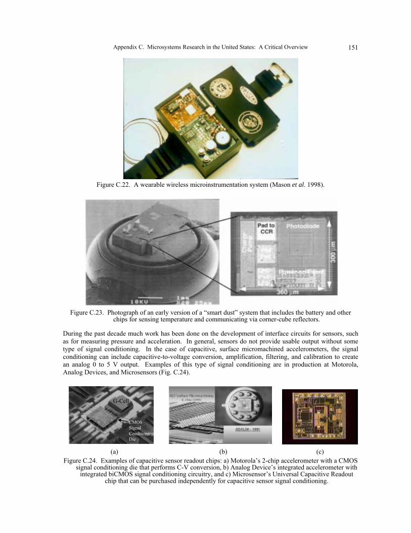
Figure C.22 shows one such wireless microinstrumentation system where a number of sensors such as pressure, acceleration, temperature, and humidity have been incorporated into a wearable module (about 7 cm long and 3.5 cm wide) that includes a microcontroller and a wireless RF link with a range of about 50 m Mason et al. 1998). Figure C.23 shows the photograph of an early version of a �smart dust� system that includes the battery and other chips for sensing temperature. These smart dust motes use an optical link for communicating information back to a host controller.
Appendix C. Microsystems Research in the United States: A Critical Overview 151
Figure C.22. A wearable wireless microinstrumentation system (Mason et al. 1998).
Figure C.23. Photograph of an early version of a �smart dust� system that includes the battery and other
chips for sensing temperature and communicating via corner-cube reflectors.
During the past decade much work has been done on the development of interface circuits for sensors, such as for measuring pressure and acceleration. In general, sensors do not provide usable output without some type of signal conditioning. In the case of capacitive, surface micromachined accelerometers, the signal conditioning can include capacitive-to-voltage conversion, amplification, filtering, and calibration to create an analog 0 to 5 V output. Examples of this type of signal conditioning are in production at Motorola, Analog Devices, and Microsensors (Fig. C.24).
G-Cell
CMOSSignal ConditioningDie
(a) (b) (c) Figure C.24. Examples of capacitive sensor readout chips: a) Motorola�s 2-chip accelerometer with a CMOS
signal conditioning die that performs C-V conversion, b) Analog Device�s integrated accelerometer with integrated biCMOS signal conditioning circuitry, and c) Microsensor�s Universal Capacitive Readout
chip that can be purchased independently for capacitive sensor signal conditioning.
Appendix C. Microsystems Research in the United States: A Critical Overview 152
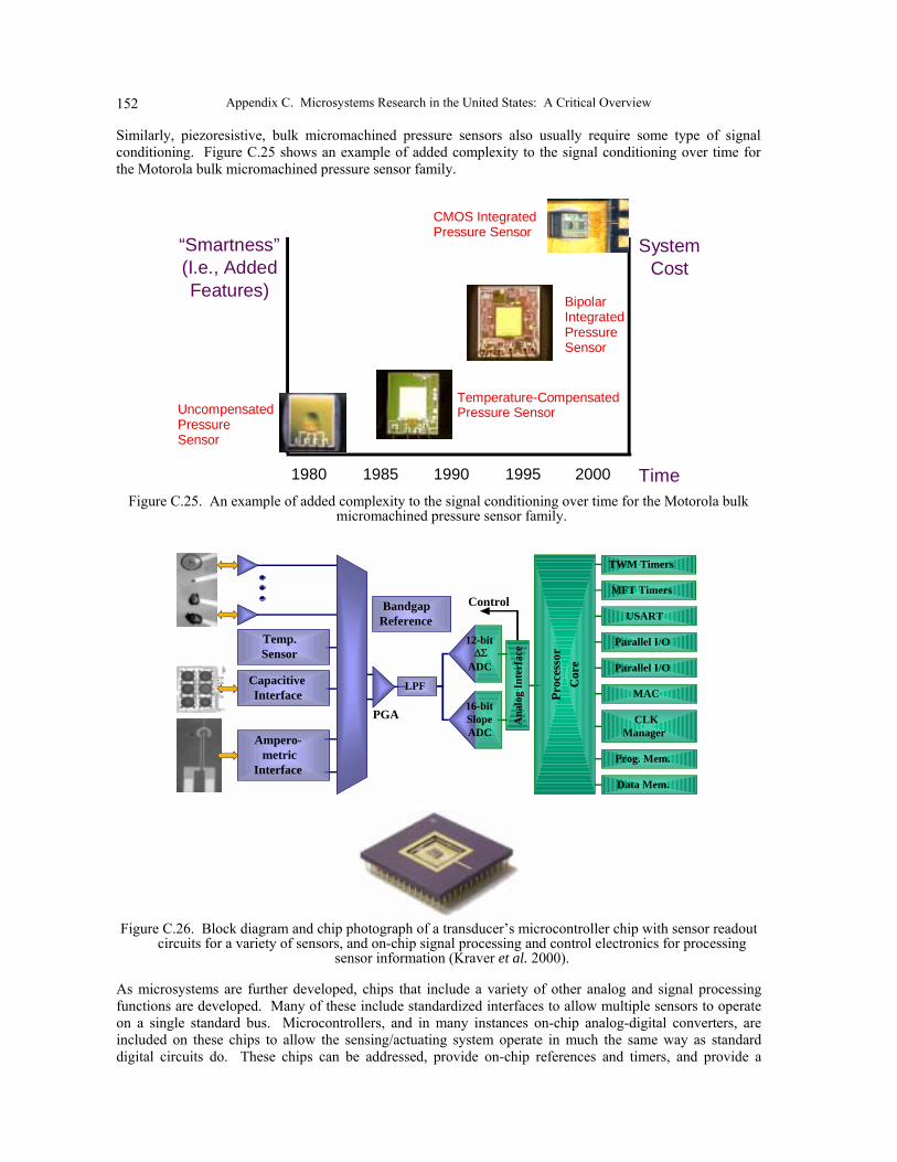
Similarly, piezoresistive, bulk micromachined pressure sensors also usually require some type of signal conditioning. Figure C.25 shows an example of added complexity to the signal conditioning over time for the Motorola bulk micromachined pressure sensor family.
“Smartness” (I.e., Added Features)
System Cost
Time 1980 1985 1990 1995 2000
Uncompensated Pressure Sensor
Temperature-Compensated Pressure Sensor
Bipolar Integrated Pressure Sensor
CMOS Integrated Pressure Sensor
Figure C.25. An example of added complexity to the signal conditioning over time for the Motorola bulk micromachined pressure sensor family.
Potentiometric Sensors
Capacitive Sensors
Amperometric Sensors
TWM Timers
MFT Timers
USART
Parallel I/O
Parallel I/O
Prog. Mem.
Data Mem.
CLKManager
MACProc
esso
rC
ore
Control
Ana
log
Inte
rfac
e
LPF
BandgapReference
PGA
12-bit∆Σ
ADC
16-bitSlopeADC
Temp.Sensor
Ampero-metric
Interface
CapacitiveInterface
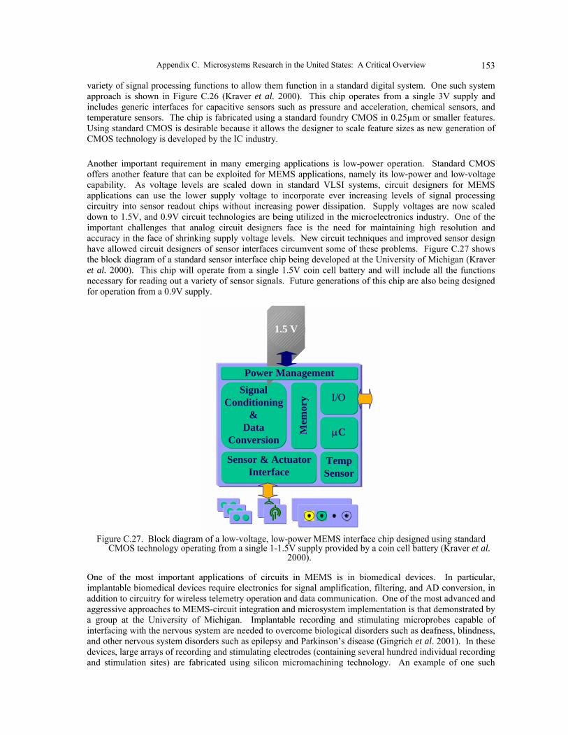
Figure C.26. Block diagram and chip photograph of a transducer�s microcontroller chip with sensor readout
circuits for a variety of sensors, and on-chip signal processing and control electronics for processing sensor information (Kraver et al. 2000).
As microsystems are further developed, chips that include a variety of other analog and signal processing functions are developed. Many of these include standardized interfaces to allow multiple sensors to operate on a single standard bus. Microcontrollers, and in many instances on-chip analog-digital converters, are included on these chips to allow the sensing/actuating system operate in much the same way as standard digital circuits do. These chips can be addressed, provide on-chip references and timers, and provide a
Appendix C. Microsystems Research in the United States: A Critical Overview 153
variety of signal processing functions to allow them function in a standard digital system. One such system approach is shown in Figure C.26 (Kraver et al. 2000). This chip operates from a single 3V supply and includes generic interfaces for capacitive sensors such as pressure and acceleration, chemical sensors, and temperature sensors. The chip is fabricated using a standard foundry CMOS in 0.25µm or smaller features. Using standard CMOS is desirable because it allows the designer to scale feature sizes as new generation of CMOS technology is developed by the IC industry.
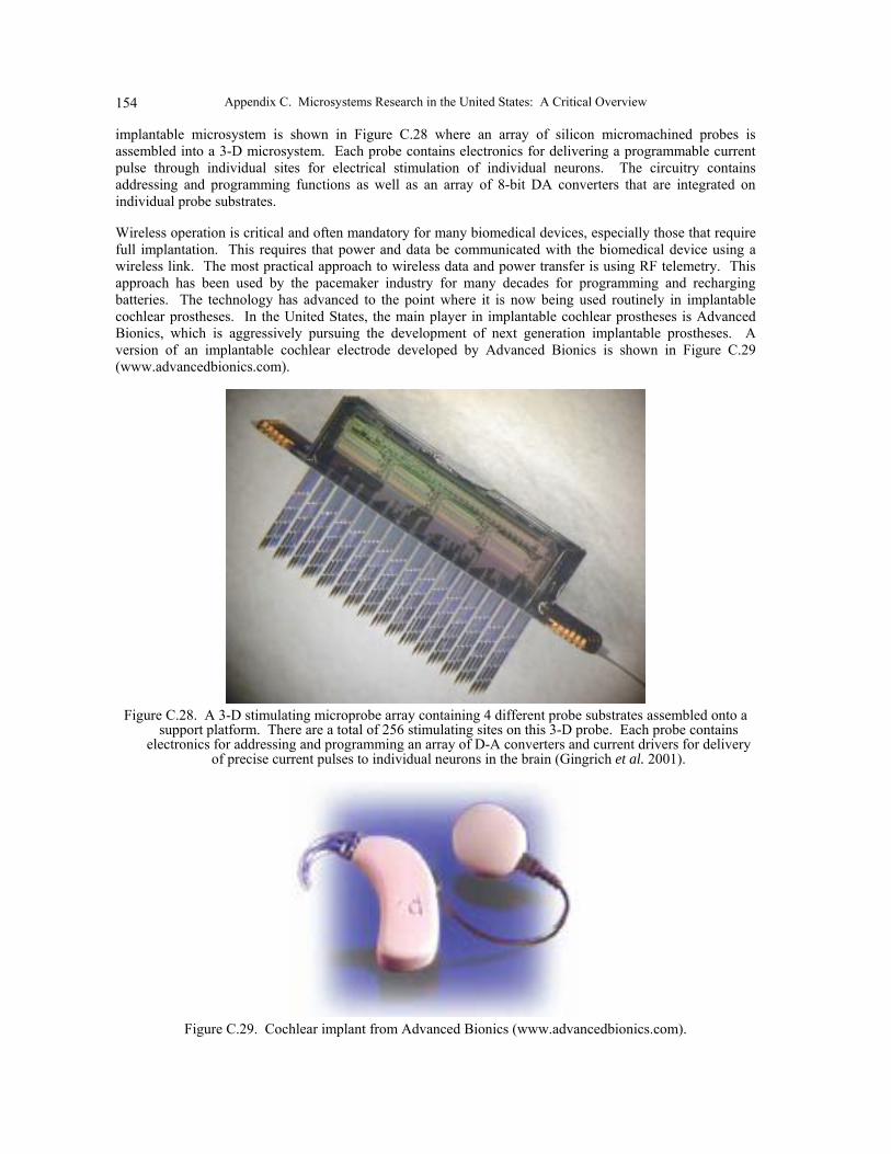
Another important requirement in many emerging applications is low-power operation. Standard CMOS offers another feature that can be exploited for MEMS applications, namely its low-power and low-voltage capability. As voltage levels are scaled down in standard VLSI systems, circuit designers for MEMS applications can use the lower supply voltage to incorporate ever increasing levels of signal processing circuitry into sensor readout chips without increasing power dissipation. Supply voltages are now scaled down to 1.5V, and 0.9V circuit technologies are being utilized in the microelectronics industry. One of the important challenges that analog circuit designers face is the need for maintaining high resolution and accuracy in the face of shrinking supply voltage levels. New circuit techniques and improved sensor design have allowed circuit designers of sensor interfaces circumvent some of these problems. Figure C.27 shows the block diagram of a standard sensor interface chip being developed at the University of Michigan (Kraver et al. 2000). This chip will operate from a single 1.5V coin cell battery and will include all the functions necessary for reading out a variety of sensor signals. Future generations of this chip are also being designed for operation from a 0.9V supply.
µC
SignalConditioning
&Data
Conversion
Ι/Ο
Sensor & ActuatorInterface
1.5 V
TempSensor
Mem
ory
Power Management
Figure C.27. Block diagram of a low-voltage, low-power MEMS interface chip designed using standard
CMOS technology operating from a single 1-1.5V supply provided by a coin cell battery (Kraver et al. 2000).
One of the most important applications of circuits in MEMS is in biomedical devices. In particular, implantable biomedical devices require electronics for signal amplification, filtering, and AD conversion, in addition to circuitry for wireless telemetry operation and data communication. One of the most advanced and aggressive approaches to MEMS-circuit integration and microsystem implementation is that demonstrated by a group at the University of Michigan. Implantable recording and stimulating microprobes capable of interfacing with the nervous system are needed to overcome biological disorders such as deafness, blindness, and other nervous system disorders such as epilepsy and Parkinson�s disease (Gingrich et al. 2001). In these devices, large arrays of recording and stimulating electrodes (containing several hundred individual recording and stimulation sites) are fabricated using silicon micromachining technology. An example of one such
Appendix C. Microsystems Research in the United States: A Critical Overview 154
implantable microsystem is shown in Figure C.28 where an array of silicon micromachined probes is assembled into a 3-D microsystem. Each probe contains electronics for delivering a programmable current pulse through individual sites for electrical stimulation of individual neurons. The circuitry contains addressing and programming functions as well as an array of 8-bit DA converters that are integrated on individual probe substrates.
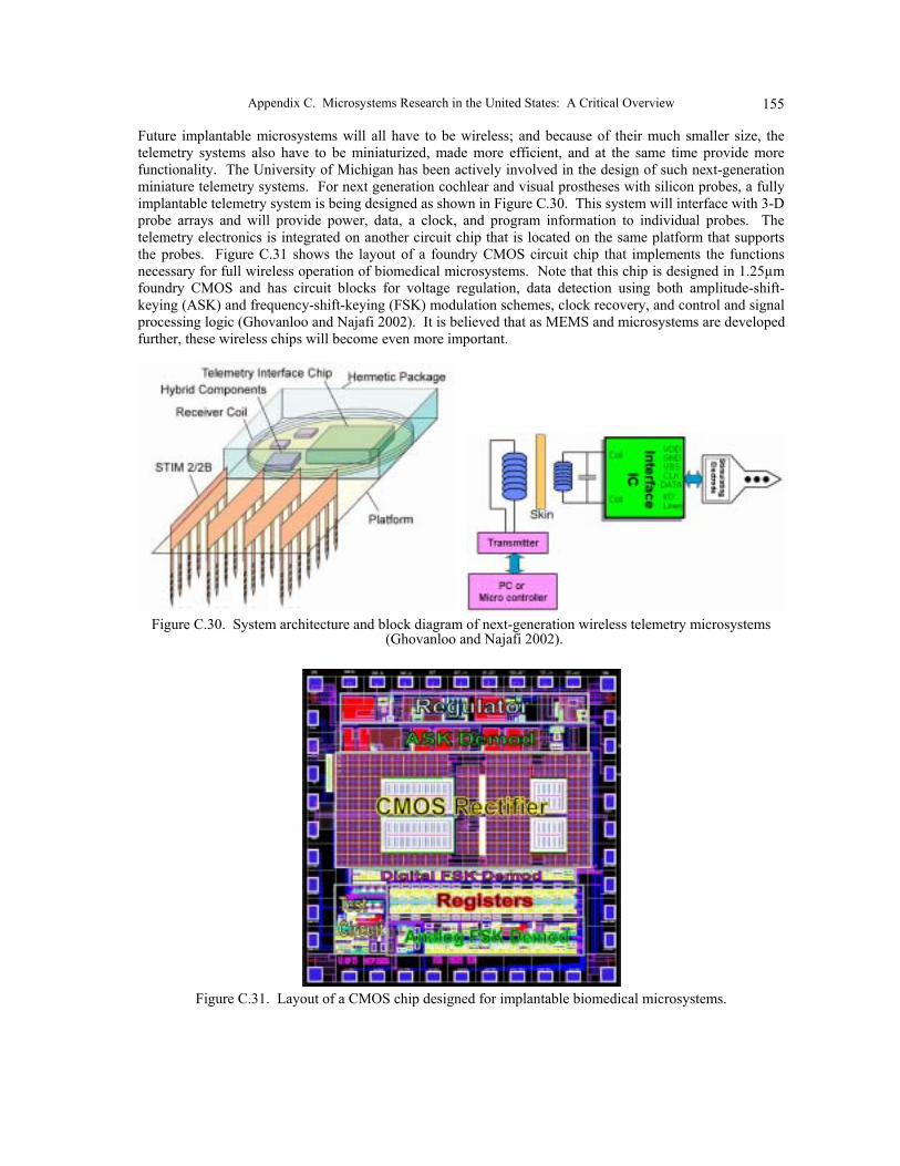
Wireless operation is critical and often mandatory for many biomedical devices, especially those that require full implantation. This requires that power and data be communicated with the biomedical device using a wireless link. The most practical approach to wireless data and power transfer is using RF telemetry. This approach has been used by the pacemaker industry for many decades for programming and recharging batteries. The technology has advanced to the point where it is now being used routinely in implantable cochlear prostheses. In the United States, the main player in implantable cochlear prostheses is Advanced Bionics, which is aggressively pursuing the development of next generation implantable prostheses. A version of an implantable cochlear electrode developed by Advanced Bionics is shown in Figure C.29 (www.advancedbionics.com).
Figure C.28. A 3-D stimulating microprobe array containing 4 different probe substrates assembled onto a
support platform. There are a total of 256 stimulating sites on this 3-D probe. Each probe contains electronics for addressing and programming an array of D-A converters and current drivers for delivery
of precise current pulses to individual neurons in the brain (Gingrich et al. 2001).
Figure C.29. Cochlear implant from Advanced Bionics (www.advancedbionics.com).
Appendix C. Microsystems Research in the United States: A Critical Overview 155
Future implantable microsystems will all have to be wireless; and because of their much smaller size, the telemetry systems also have to be miniaturized, made more efficient, and at the same time provide more functionality. The University of Michigan has been actively involved in the design of such next-generation miniature telemetry systems. For next generation cochlear and visual prostheses with silicon probes, a fully implantable telemetry system is being designed as shown in Figure C.30. This system will interface with 3-D probe arrays and will provide power, data, a clock, and program information to individual probes. The telemetry electronics is integrated on another circuit chip that is located on the same platform that supports the probes. Figure C.31 shows the layout of a foundry CMOS circuit chip that implements the functions necessary for full wireless operation of biomedical microsystems. Note that this chip is designed in 1.25µm foundry CMOS and has circuit blocks for voltage regulation, data detection using both amplitude-shift-keying (ASK) and frequency-shift-keying (FSK) modulation schemes, clock recovery, and control and signal processing logic (Ghovanloo and Najafi 2002). It is believed that as MEMS and microsystems are developed further, these wireless chips will become even more important.
Figure C.30. System architecture and block diagram of next-generation wireless telemetry microsystems
(Ghovanloo and Najafi 2002).
Figure C.31. Layout of a CMOS chip designed for implantable biomedical microsystems.
Appendix C. Microsystems Research in the United States: A Critical Overview 156
REFERENCES
Ghovanloo, M., and K. Najafi. Paper to be published in 2002. University of Michigan.
Gingrich, M.D., J.F. Hetke, D.J. Anderson, and K.D. Wise. 2001. A 256-site CMOS microelectrode array for multipoint stimulation and recording in the central nervous system. Digest, Int. Conf. On Solid-State Sensors and Actuators, Transducers 2001, pp. 416-19.
Kraver, K.L., M.R. Gutthaus, T.D. Strong, P.L. Bird, G.S. Cha, W. Hold, and R.B. Brown. 2000. A mixed-signal sensor interface microinstrument. Technical Digest, Hilton Head Solid-State Sensor and Actuator Workshop, pp. 14-17.
Mason, A.J., N. Yazdi, A.V. Chavan, K. Najafi, and K.D. Wise. 1998. A generic multi-element microsystem for portable wireless applications (invited paper). Special Issue of IEEE Proceedings, 86 (8): 1733-1746.
Warneke, B., B. Atwood, and K. S.J. Pister. 2001. Smart dust mote forerunners. Technical Digest, IEEE MEMS Conference, pp. 357-360.
Wise, K.D., K. Najafi, D.M. Aslam, R.B. Brown, J.M. Giachino, L.C. McAfee, C.T.-C. Nguyen, R.O. Warrington, and E.T. Zellers. 2001. Wireless integrated microsystems (WIMS): the coming revolution in the remote gathering of information. Digest SensorsExpo, (Symposium Keynote), Chicago, June.
Zee, F., and J.W. Judy. 2001. Micromachined polymer-based chemical gas sensor array. Sensors and Actuators B 72: 120-128.
BACKEND PROCESSES AND TECHNOLOGIES
Packaging, assembly, trimming/calibration, and testing MEMS/MST devices represent a considerable portion of the cost of MEMS/MST products. Swift (1998) and Schuster (1998) both showed that packaging and testing can represent over 50% of the product cost for a microsystem. Discussion during each of the last two �Commercialization of Microsystems� conferences has confirmed this point. In fact, often industrial MEMS engineers and managers suggest that a typical cost breakdown is roughly 33% silicon content, 33% package, and 33% test. It has been reported, in some cases, as greater than 70% packaging cost vs. silicon content (Madou 1997; Allan 1997; Reichl 1991; Song 1997; Eddy and Sparks 1998; Beardmore 1997). Furthermore, of this silicon content, often less than half the cost is due to the microsensor or actuators. The rest of the silicon content is the control or interface electronics cost.
A complete overview of the backend assembly and test technologies can be found in Chapter 7 of P. Rai-Choudhury�s MEMS and MOEMS: Technology and Applications (2000). The section represents a summary of that review. Packaging MEMS/MST devices poses unique challenges when compared with more conventional electronic packaging because the MEM device can mistake physical signals induced by the package for signals from the environment (Ristic and Shah 1996). This problem was observed very early in the development of sensors and actuators. Senturia and Smith noted, �it is necessary to design the microsensor and the package AT THE SAME TIME� (1988). They made two very important observations in this work: �Packaging people� and �sensor people� are usually not the same people, and they do not always work well together; and consideration of the package can help eliminate possible sensor designs because they would not be feasible in a particular package.
The package can play a vital functional role in the productization of a microsystem. For example, the package can isolate the induced stress from the mounting of the device (Eddy and Sparks 1998; Bicking et al. 1985); it can make the electronics compatible with the harsh environment (Eddy and Sparks 1998; Ristic and M. Shah 1996); and it can even be an integral part of the microsystem (e.g., mechatronics packaging). While MEMS engineers often discuss integration as a technique for placing transducers and electronics on the same IC chip, integration can also refer to the combination of typical package functions onto the silicon (Ristic and M. Shah 1996; Wise 1991). Wafer bonding is an example of this. In pressure sensors, an absolute vacuum reference can be integrated into the silicon device. Furthermore, many microsystems will not be integrated monolithically; therefore, multichip packaging will be required (Wise 1991).
Finally, efforts of packaging and testing for MEMS have been significantly under-represented in academic and trade publications. Considering the cost breakdown, little has been written on the assembly and test for MEMS. Much of the grant money, academic research, and publications are on the micromachined transducer
Appendix C. Microsystems Research in the United States: A Critical Overview 157
itself and not the rest of the microsystem. Recently, that point has been highlighted in several conferences (Solid-State Sensors and Actuators 1998; Commercialization of Microsystems 1996 and 1998). Publications that have summarized the slow breakthrough of microsystems into commercial application have pointed to the following limitations of the technology (Allan 1997; Commercialization of Microsystems 1996 and 1998; Detlefs 1998):
• CAD • Standards • Assembly techniques (Wise 1991) • Process tools (both front-end and back-end tools) • Test equipment, processes and standards • Harsh media compatibility (Madou 1997; Ristic and Shah 1996; Detlefs 1998) • Reliability standards and results • Packaging techniques and processes
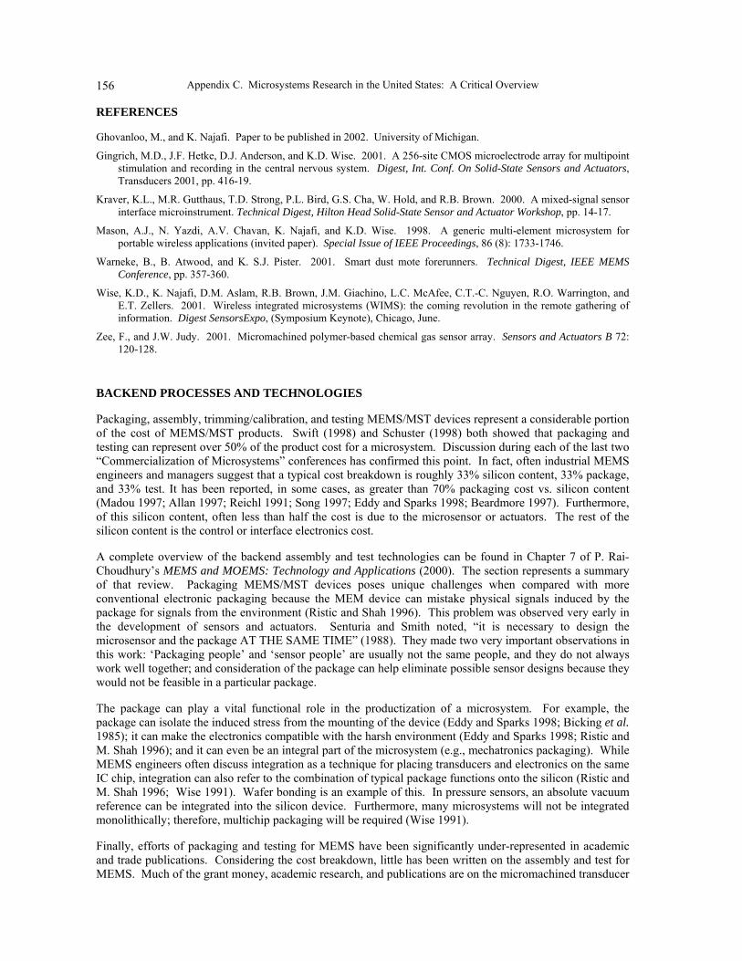
To create MEMS packages, the following common processes are used: bonding, wafer sawing/scribing, pick and place, die attach, wirebonding/interconnection, encapsulation, overmolding, trimming, and final testing. Figure C.32 shows a typical flow diagram for assembly. Specifically, this is an example of a pressure sensor assembly and test flow.
Figure C.32. An example flow diagram for a typical pressure sensor assembly process flow.
In the case of absolute pressure sensors, wafer-level packaging is used (Fig. C.33) to create an absolute vacuum reference. Similarly, some accelerometers or micromachined resonators also require wafer-level bonding to create a controlled atmosphere for the device (Fig. C.34). Complete reviews of wafer-to-wafer bonding for MEMS are given by Schmidt (1998) and Ko et al. (1985).

Appendix C. Microsystems Research in the United States: A Critical Overview 158
Figure C.33. Wafer bonding to create an absolute vacuum cavity for an absolute pressure sensor device
(Ristic 1994).
Figure C.34. Motorola two-chip accelerometer. The micromachined device is located within the wafer-
bonded die (right side). Wafer bonding is done using an adhesive glass frit for the hermetic wafer-level sealing of an accelerometer device prior to wafer saw and assembly (Ristic 1994).
Appendix C. Microsystems Research in the United States: A Critical Overview 159
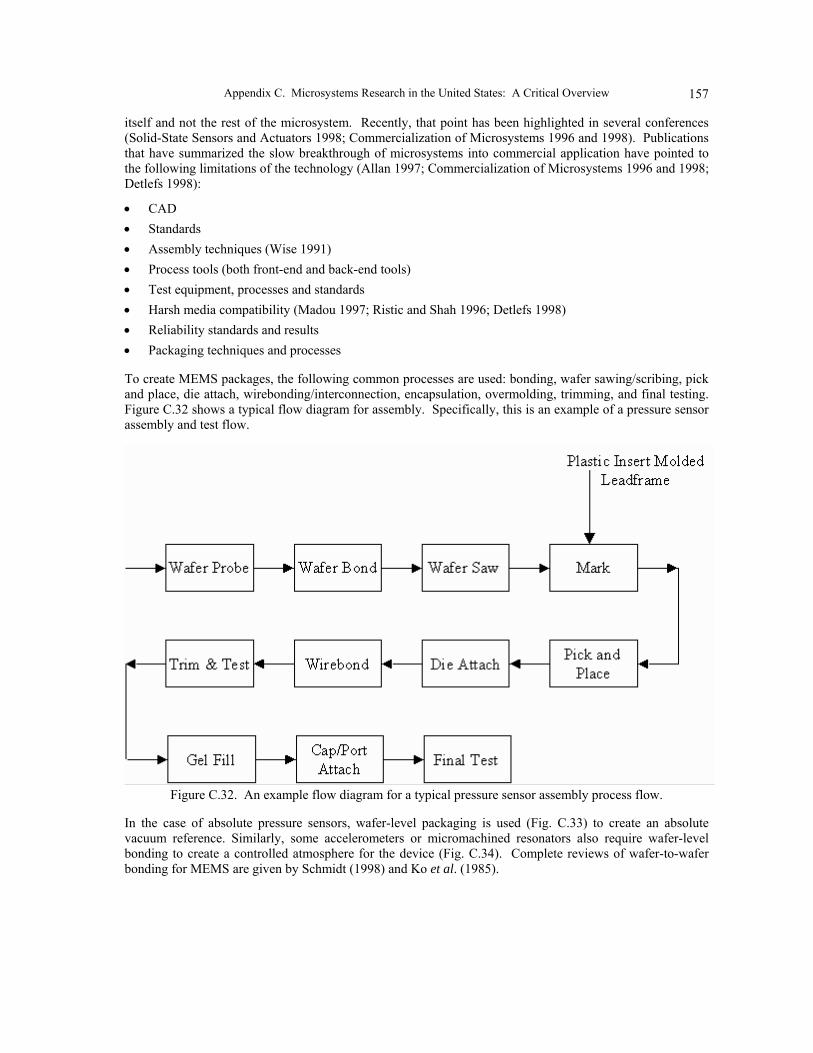
Besides protecting the device in operation, the wafer-bonded accelerometer in Figure C.34 is also protected during the assembly process, including during wafer sawing (Ristic and Shah 1996; Kniffin and Shah 1996). However, in the case of the Analog Devices production accelerometer, wafer-level packaging is not employed, so a special upside-down sawing process is used (Figure C.35).
Figure C.35. Upside-down wafer sawing process used to protect the Analog Devices accelerometer during
die separation (Chau and Sulouff 1998).
Following this die separation, a modified pick and place tool is used to minimize the disturbance of the surface micromachined structure during the operation (Chau and Sulouff 1998). Some research has been performed over the past several years in the United States to investigate the possibility of self-assembly. Yeh et al. have observed trapping of semiconductor ICs in micromachined wells (1994). Cohn et al. have modified this technique by adding electrostatic alignment of the die prior to settling into the cavities (1995). After the die is bonded onto the substrate, wirebonding and final encapsulation, sealing, or overmolding is performed. Figure C.36 shows some MEMS packages.
In high volume manufacturing, a distribution of electrical parameters from device to device is observed. The method for minimizing the effect of that variation on yield loss is called trimming. Manual calibration, laser trimming, zener zap, electronic calibration (Summers et al. 1996), polysilicon resistor trimming (Feldbaumer et al. 1995; Ryan and Bryzek 1995), E/EPROM, and other methods are used for this purpose. In the case of a Motorola bipolar pressure sensor or an Analog Devices accelerometer, the device is laser trimmed.

Appendix C. Microsystems Research in the United States: A Critical Overview 160
(a) (b)
(c) (d)
(e) (f)
(g) (h)
(i) (j)
Appendix C. Microsystems Research in the United States: A Critical Overview 161
(k) (l)
(m) (n)
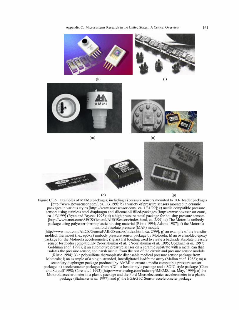
(o) (p) Figure C.36. Examples of MEMS packages, including a) pressure sensors mounted to TO-Header packages
[http://www.novasensor.com/, ca. 1/31/99]; b) a variety of pressure sensors mounted in ceramic packages in various styles [http: //www.novasensor.com/, ca. 1/31/99]; c) media compatible pressure
sensors using stainless steel diaphragm and silicone oil filled-packages [http: //www.novasensor.com/, ca. 1/31/99] (Ryan and Bryzek 1995); d) a high pressure metal package for housing pressure sensors [http://www.mot.com/AECS/General/AIEGSensors/index.html, ca. 2/99]; e) The Motorola unibody package using polyester thermoplastic housing material (Ristic 1994; Adams 1987); f) the Motorola
manifold absolute pressure (MAP) module [http://www.mot.com/AECS/General/AIEGSensors/index.html, ca. 2/99]; g) an example of the transfer-molded, thermoset (i.e., epoxy) unibody pressure sensor package by Motorola; h) an overmolded epoxy package for the Motorola accelerometer; i) glass frit bonding used to create a backside absolute pressure
sensor for media compatibility (Sooriakumar et al. ; Sooriakumar et al. 1995; Goldman et al. 1997; Goldman et al. 1998); j) an automotive pressure sensor on a ceramic substrate with a metal can that isolates the pressure sensor, and harsh media, from the rest of the circuit and pressure sensor module
(Ristic 1994); k) a polysulfone thermoplastic disposable medical pressure sensor package from Motorola; l) an example of a single-stranded, interdigitated leadframe array (Mallon et al. 1988); m) a
secondary diaphragm package produced by AMMI to create a media compatible pressure sensor package; n) accelerometer packages from ADI�a header-style package and a SOIC-style package (Chau
and Sulouff 1998; Core et al. 1993) [http://www.analog.com/industry/iMEMS/, ca. May, 1999]; o) the Motorola accelerometer in a plastic package and the Ford Microelectronics accelerometer in a plastic
package (Stalnaker et al. 1997); and p) the EG&G IC Sensor accelerometer package.
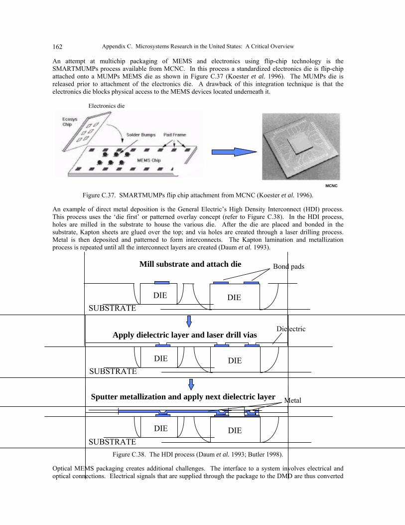
Appendix C. Microsystems Research in the United States: A Critical Overview 162
An attempt at multichip packaging of MEMS and electronics using flip-chip technology is the SMARTMUMPs process available from MCNC. In this process a standardized electronics die is flip-chip attached onto a MUMPs MEMS die as shown in Figure C.37 (Koester et al. 1996). The MUMPs die is released prior to attachment of the electronics die. A drawback of this integration technique is that the electronics die blocks physical access to the MEMS devices located underneath it.
MCNC
Electronics die
Figure C.37. SMARTMUMPs flip chip attachment from MCNC (Koester et al. 1996).
An example of direct metal deposition is the General Electric�s High Density Interconnect (HDI) process. This process uses the �die first� or patterned overlay concept (refer to Figure C.38). In the HDI process, holes are milled in the substrate to house the various die. After the die are placed and bonded in the substrate, Kapton sheets are glued over the top; and via holes are created through a laser drilling process. Metal is then deposited and patterned to form interconnects. The Kapton lamination and metallization process is repeated until all the interconnect layers are created (Daum et al. 1993).
SUBSTRATEDIE DIE
Mill substrate and attach die
Apply dielectric layer and laser drill vias
Sputter metallization and apply next dielectric layer
Bond pads
Dielectric
SUBSTRATEDIE DIE
Metal
SUBSTRATEDIE DIE
Figure C.38. The HDI process (Daum et al. 1993; Butler 1998).
Optical MEMS packaging creates additional challenges. The interface to a system involves electrical and optical connections. Electrical signals that are supplied through the package to the DMD are thus converted
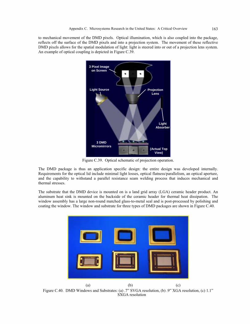
Appendix C. Microsystems Research in the United States: A Critical Overview 163
to mechanical movement of the DMD pixels. Optical illumination, which is also coupled into the package, reflects off the surface of the DMD pixels and into a projection system. The movement of these reflective DMD pixels allows for the spatial modulation of light: light is steered into or out of a projection lens system. An example of optical coupling is depicted in Figure C.39.
Light Source Projection Lens
Light Absorber
3 DMDMicromirrors
3 Pixel Image on Screen
(Actual Top View)
Light Source Projection Lens
Light Absorber
3 DMDMicromirrors
3 Pixel Image on Screen
(Actual Top View)
Figure C.39. Optical schematic of projection operation.
The DMD package is thus an application specific design: the entire design was developed internally. Requirements for the optical lid include minimal light losses, optical flatness/parallelism, an optical aperture, and the capability to withstand a parallel resistance seam welding process that induces mechanical and thermal stresses.
The substrate that the DMD device is mounted on is a land grid array (LGA) ceramic header product. An aluminum heat sink is mounted on the backside of the ceramic header for thermal heat dissipation. The window assembly has a large non-round matched glass-to-metal seal and is post-processed by polishing and coating the window. The window and substrate for three types of DMD packages are shown in Figure C.40.
(a) (b) (c)
Figure C.40. DMD Windows and Substrates: (a) .7� SVGA resolution, (b) .9� XGA resolution, (c) 1.1� SXGA resolution

Appendix C. Microsystems Research in the United States: A Critical Overview 164
The lid assembly consists of two-piece parts, a stamped kovar frame and Corning 7056 glass. Packaging material selection, especially matching coefficients of thermal expansion (CTE), is important for a mechanical and environmental robust package. Since the CTE of the metal and glass are very close, a matched glass-to-metal seal is made by means of a belt furnace with a peak temperature of approximately 1000oC. After the glass-to-metal fuse is complete, the glass of the window assembly is processed through a double-sided grinding and polishing operation. The kovar frame is then plated with 2-8 µm of nickel and a minimum of 1-2 µm of gold. It is important that the surface quality of the glass not be damaged when the polished window assembly is exposed to the chemical baths during the plating process.
Two coatings are then applied to the window assembly. First, a low reflectance coating is applied on the surface of the glass that will be on the inside of the package after the window-attach process. A photomask is applied, and this low reflectance coating is removed or etched away to form a clear window aperture. To achieve a sharp aperture edge definition (i.e., less than 20 µm protrusions), the etch chemistry and process time used during the process are critical. The purpose of the window aperture is to hide features outside of the DMD active array. Features such as bond wires are blocked from the illumination source. After the aperture coating is etched, the photomask is removed and MgF2 antireflective (AR) coatings are applied to both sides of the glass. The required average transmittance of the AR coatings is greater than 98%, and the reflectance is less than 0.5%. Finally, two getter strips are adhesively attached to the internal region of the window assembly. The purpose of the getter is to control contaminants (specifically moisture). Stiction mitigation is the primary driver for the inclusion of the getter strips: Moisture (i.e., capillary attraction) can cause the pixel to stick upon landing. The complete package is shown in Figure C.41.
Figure C.41. Side view of DMD hermetic package.
Finally, MCNC/Cronos has recently introduced a microrelay product (Figure C.42). Initial shipments are based on ceramic packages, while an injection molded plastic version is planned for future production (Paultre 1999). The package is PCM-CIA compliant and contains from two to eight switches per package. Each switch is electrically tested to insure that it conforms to specifications. Reliability tests have shown that these devices perform within specifications at over a million cycles. Their robust relay design lends itself well to conventional packaging technology and does not place unusual requirements on the packaging.
Figure C.42. Cronos Integrated Microsystems (formerly MCNC MEMS Technology Center) microrelay
product.
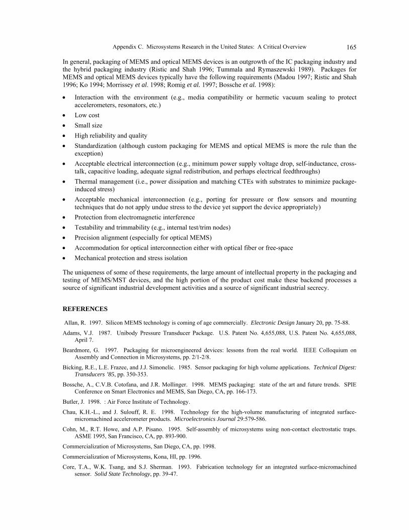
Appendix C. Microsystems Research in the United States: A Critical Overview 165
In general, packaging of MEMS and optical MEMS devices is an outgrowth of the IC packaging industry and the hybrid packaging industry (Ristic and Shah 1996; Tummala and Rymaszewski 1989). Packages for MEMS and optical MEMS devices typically have the following requirements (Madou 1997; Ristic and Shah 1996; Ko 1994; Morrissey et al. 1998; Romig et al. 1997; Bossche et al. 1998):
• Interaction with the environment (e.g., media compatibility or hermetic vacuum sealing to protect accelerometers, resonators, etc.)
• Low cost • Small size • High reliability and quality • Standardization (although custom packaging for MEMS and optical MEMS is more the rule than the
exception) • Acceptable electrical interconnection (e.g., minimum power supply voltage drop, self-inductance, cross-
talk, capacitive loading, adequate signal redistribution, and perhaps electrical feedthroughs) • Thermal management (i.e., power dissipation and matching CTEs with substrates to minimize package-
induced stress) • Acceptable mechanical interconnection (e.g., porting for pressure or flow sensors and mounting
techniques that do not apply undue stress to the device yet support the device appropriately) • Protection from electromagnetic interference • Testability and trimmability (e.g., internal test/trim nodes) • Precision alignment (especially for optical MEMS) • Accommodation for optical interconnection either with optical fiber or free-space • Mechanical protection and stress isolation
The uniqueness of some of these requirements, the large amount of intellectual property in the packaging and testing of MEMS/MST devices, and the high portion of the product cost make these backend processes a source of significant industrial development activities and a source of significant industrial secrecy.
REFERENCES
Allan, R. 1997. Silicon MEMS technology is coming of age commercially. Electronic Design January 20, pp. 75-88.
Adams, V.J. 1987. Unibody Pressure Transducer Package. U.S. Patent No. 4,655,088, U.S. Patent No. 4,655,088, April 7.
Beardmore, G. 1997. Packaging for microengineered devices: lessons from the real world. IEEE Colloquium on Assembly and Connection in Microsystems, pp. 2/1-2/8.
Bicking, R.E., L.E. Frazee, and J.J. Simonelic. 1985. Sensor packaging for high volume applications. Technical Digest: Transducers ’85, pp. 350-353.
Bossche, A., C.V.B. Cotofana, and J.R. Mollinger. 1998. MEMS packaging: state of the art and future trends. SPIE Conference on Smart Electronics and MEMS, San Diego, CA, pp. 166-173.
Butler, J. 1998. : Air Force Institute of Technology.
Chau, K.H.-L., and J. Sulouff, R. E. 1998. Technology for the high-volume manufacturing of integrated surface-micromachined accelerometer products. Microelectronics Journal 29:579-586.
Cohn, M., R.T. Howe, and A.P. Pisano. 1995. Self-assembly of microsystems using non-contact electrostatic traps. ASME 1995, San Francisco, CA, pp. 893-900.
Commercialization of Microsystems, San Diego, CA, pp. 1998.
Commercialization of Microsystems, Kona, HI, pp. 1996.
Core, T.A., W.K. Tsang, and S.J. Sherman. 1993. Fabrication technology for an integrated surface-micromachined sensor. Solid State Technology, pp. 39-47.
Appendix C. Microsystems Research in the United States: A Critical Overview 166
Daum, W., W. Burdick Jr., and R. Fillion. 1993. Overlay high-density interconnect: a chips-first multichip module technology. IEEE Computer 26:23-29.
Detlefs, B. 1998. MEMS 1998: Emerging Applications and Markets. November 19.
Eddy, D.S., and D.R. Sparks. 1998. Application of MEMS technology in automotive sensors and actuators. Proceedings of the IEEE 86: 1747-1755.
Feldbaumer, D.W., and J.A. Babcock. 1995. Theory and application of polysilicon resistor trimming. Sold-State Electronics 38:1861-1869.
Feldbaumer, D.W., J.A. Babcock, V.M. Mercier, and C.K.Y. Chun. 1995. Pulse current trimming of polysilicon resistors. IEEE Trans. Electron Devices 42:689-696.
Goldman, K., G. Gritt, I. Baskett, K. Sooriakumar, D. Wallace, D. Hughes, and M. Shah. 1997. A vertically integrated media-isolated absolute pressure sensor. Transducers ’97: 1997 International Conference on Solid-State Sensors and Actuators, Chicago, IL, pp. 1501-1504.
Goldman, K., G. Gritt, I. Baskett, W. Czarnocki, A. Ramirez, C. Brown, D. Hughes, D. Wallace, and M. Shah. 1998. A vertically integrated media-isolated absolute pressure sensor. Sensors and Actuators A 66:155-159.
Kniffin, M.L., and M. Shah. 1996. Packaging for silicon micromachined accelerometers. The International Journal of Microcircuits and Electronic Packaging 19:75-86.
Ko, W.H. 1994. Packaging of microsensors. Microsystems Technologies ’94: Proc. 4th International Conference and Exhibition on Micro Electro Mechanical Systems and Components, pp. 477-480.
Ko, W.H., J.T. Suminto, and G.J. Yeh. 1985. Bonding techniques for microsensors. In Micromachining and Micropackaging of Transducers, C.D. Fung, P.W. Cheung, W.H. Ko, and D.G. Fleming, Eds. Amsterdam: Elsevier Science Publishers B. V., pp. 41-61.
Koester, D., R. Mahadevan, A. Shishkoff, and K. Markus. 1996. Multi-user MEMS processes (MUMPS) introduction and design rules, rev. 4. July 15.
Madou, M. 1997. Fundamentals of Microfabrication. Boca Raton, FL: CRC Press.
Mallon, J., J. Bryzek, J. Ramsey, G. Tomblin, and F. Pourahmadi. 1988. Low-cost, high-volume packaging techniques for silicon sensors and actuators. Presented at the IEEE Solid-State Sensor and Actuator Workshop, Hilton Head Island, S.C., pp. 123-124.
Morrissey, A., G. Kelly, and J. Alderman. 1998. Low-stress 3-D packaging of a microsystem. Sensors and Actuators A 68:404-409.
Paultre, A. 1999. Microrelay brings MEMS technology to commercial market. Electronic Products Magazine February: p. 28.
Rai-Choudhury, P. 2000. MEMS and MOEMS: Technology and Applications. SPIE Press Monograph.
Reichl, H. 1991. Packaging and interconnection of sensors. Sensors and Actuators, A25- A27: 63-71.
Ristic, L. 1994. Sensor technology and devices. Boston, MA: Artech House, p. 524.
Ristic, L., and M. Shah. 1996. Trends in MEMS technology. WESCON 96 Conference Proceedings, Anaheim, CA, pp. 64-72.
Romig, J., A.D., P.V. Dressendorfer, and D.W. Palmer. 1997. High performance microsystem packaging: a perspective. Microelectron. Reliab. 37:1771-1781.
Ryan, K., and J. Bryzek. 1995. Packaging technology for low-cost media isolated pressure sensors. Sensor 95, Kongreßband, pp. 685-690.
Schmidt, M.A. 1998. Wafer-to-wafer bonding for microstructure formation. Proceedings of the IEEE 86:1575-1585.
Schuster, J. 1998. Rump Session. Solid-state Sensors and Actuators Workshop, Hilton Head Island, S.C., pp. 1998.
Senturia, S.D., and R.L. Smith. 1988. Microsensor packaging and system partitioning. Sensors and Actuators 15:221-234.
Solid-State Sensors and Actuators Workshop, Hilton Head Island, S.C., pp. 1998.
Song, C. 1997. Commercial vision of silicon based inertial sensors. Transducers '97: International Conference on Solid-State Sensors and Actuators, Chicago, IL, pp. 839-842.
Sooriakumar, K., D. J. Monk, W. K. Chan, and K. G. Goldman. Vertically Integrated Sensor Structure and Method.
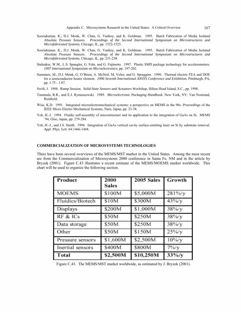
Appendix C. Microsystems Research in the United States: A Critical Overview 167
Sooriakumar, K., D.J. Monk, W. Chan, G. Vanhoy, and K. Goldman. 1995. Batch Fabrication of Media Isolated Absolute Pressure Sensors. Proceedings of the Second International Symposium on Microstructures and Microfabricated Systems, Chicago, IL, pp. 1522-1523.
Sooriakumar, K., D.J. Monk, W. Chan, G. Vanhoy, and K. Goldman. 1995. Batch Fabrication of Media Isolated Absolute Pressure Sensors. Proceedings of the Second International Symposium on Microstructures and Microfabricated Systems, Chicago, IL, pp. 231-238.
Stalnaker, W.M., L.S. Spangler, G. Fehr, and G. Fujimoto. 1997. Plastic SMD package technology for accelerometers. 1997 International Symposium on Microelectronics, pp. 197-202.
Summers, M., D.J. Monk, G. O�Brien, A. McNeil, M. Velez, and G. Spraggins. 1996. Thermal electric FEA and DOE for a semiconductor heater element. 1996 Seventh International ANSYS Conference and Exhibition, Pittsburgh, PA, pp. 1.75 - 1.87.
Swift, J. 1998. Rump Session. Solid-State Sensors and Actuators Workshop, Hilton Head Island, S.C., pp. 1998.
Tummala, R.R., and E.J. Rymaszewski. 1989. Microelectronic Packaging Handbook. New York, NY: Van Nostrand, Reinhold.
Wise, K.D. 1991. Integrated microelectromechanical systems: a perspective on MEMS in the 90s. Proceedings of the IEEE Micro Electro Mechanical Systems, Nara, Japan, pp. 33-38.
Yeh, H.-J. 1994. Fluidic self-assembly of microstructure and its application to the integration of GaAs on Si. MEMS �94, Oiso, Japan, pp. 279-284.
Yeh, H.-J., and J.S. Smith. 1994. Integration of GaAs vertical cavity surface-emitting laser on Si by substrate removal. Appl. Phys. Lett. 64:1466-1468.
COMMERCIALIZATION OF MICROSYSTEMS TECHNOLOGIES
There have been several overviews of the MEMS/MST market in the United States. Among the most recent are from the Commercialization of Microsystems 2000 conference in Santa Fe, NM and in the article by Bryzek (2001). Figure C.43 illustrates a recent estimate of the MEMS/MOEMS market worldwide. This chart will be used to organize the following section.
Figure C.43. The MEMS/MST market worldwide, as estimated by J. Bryzek (2001).
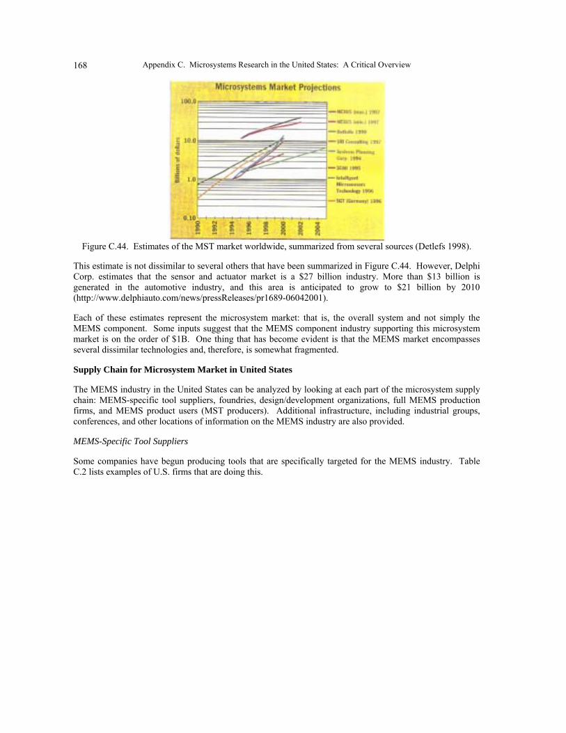
Appendix C. Microsystems Research in the United States: A Critical Overview 168
Figure C.44. Estimates of the MST market worldwide, summarized from several sources (Detlefs 1998).
This estimate is not dissimilar to several others that have been summarized in Figure C.44. However, Delphi Corp. estimates that the sensor and actuator market is a $27 billion industry. More than $13 billion is generated in the automotive industry, and this area is anticipated to grow to $21 billion by 2010 (http://www.delphiauto.com/news/pressReleases/pr1689-06042001).
Each of these estimates represent the microsystem market: that is, the overall system and not simply the MEMS component. Some inputs suggest that the MEMS component industry supporting this microsystem market is on the order of $1B. One thing that has become evident is that the MEMS market encompasses several dissimilar technologies and, therefore, is somewhat fragmented.
Supply Chain for Microsystem Market in United States
The MEMS industry in the United States can be analyzed by looking at each part of the microsystem supply chain: MEMS-specific tool suppliers, foundries, design/development organizations, full MEMS production firms, and MEMS product users (MST producers). Additional infrastructure, including industrial groups, conferences, and other locations of information on the MEMS industry are also provided.
MEMS-Specific Tool Suppliers
Some companies have begun producing tools that are specifically targeted for the MEMS industry. Table C.2 lists examples of U.S. firms that are doing this.
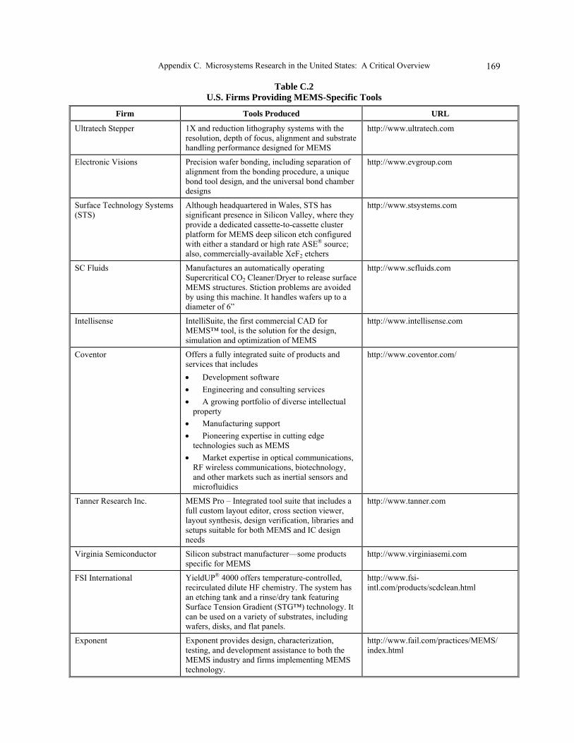
Appendix C. Microsystems Research in the United States: A Critical Overview 169
Table C.2 U.S. Firms Providing MEMS-Specific Tools
Firm Tools Produced URL
Ultratech Stepper 1X and reduction lithography systems with the resolution, depth of focus, alignment and substrate handling performance designed for MEMS
http://www.ultratech.com
Electronic Visions Precision wafer bonding, including separation of alignment from the bonding procedure, a unique bond tool design, and the universal bond chamber designs
http://www.evgroup.com
Surface Technology Systems (STS)
Although headquartered in Wales, STS has significant presence in Silicon Valley, where they provide a dedicated cassette-to-cassette cluster platform for MEMS deep silicon etch configured with either a standard or high rate ASE® source; also, commercially-available XeF2 etchers
http://www.stsystems.com
SC Fluids Manufactures an automatically operating Supercritical CO2 Cleaner/Dryer to release surface MEMS structures. Stiction problems are avoided by using this machine. It handles wafers up to a diameter of 6�
http://www.scfluids.com
Intellisense IntelliSuite, the first commercial CAD for MEMS� tool, is the solution for the design, simulation and optimization of MEMS
http://www.intellisense.com
Coventor Offers a fully integrated suite of products and services that includes • Development software • Engineering and consulting services • A growing portfolio of diverse intellectual
property • Manufacturing support • Pioneering expertise in cutting edge
technologies such as MEMS • Market expertise in optical communications,
RF wireless communications, biotechnology, and other markets such as inertial sensors and microfluidics
http://www.coventor.com/
Tanner Research Inc. MEMS Pro � Integrated tool suite that includes a full custom layout editor, cross section viewer, layout synthesis, design verification, libraries and setups suitable for both MEMS and IC design needs
http://www.tanner.com
Virginia Semiconductor Silicon substract manufacturer�some products specific for MEMS
http://www.virginiasemi.com
FSI International YieldUP® 4000 offers temperature-controlled, recirculated dilute HF chemistry. The system has an etching tank and a rinse/dry tank featuring Surface Tension Gradient (STG�) technology. It can be used on a variety of substrates, including wafers, disks, and flat panels.
http://www.fsi-intl.com/products/scdclean.html
Exponent Exponent provides design, characterization, testing, and development assistance to both the MEMS industry and firms implementing MEMS technology.
http://www.fail.com/practices/MEMS/ index.html
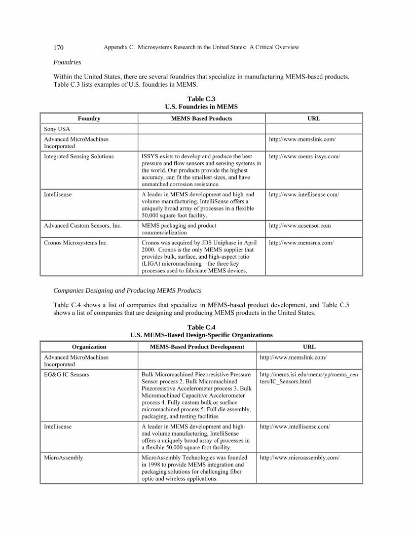
Appendix C. Microsystems Research in the United States: A Critical Overview 170
Foundries
Within the United States, there are several foundries that specialize in manufacturing MEMS-based products. Table C.3 lists examples of U.S. foundries in MEMS.
Table C.3 U.S. Foundries in MEMS
Foundry MEMS-Based Products URL
Sony USA
Advanced MicroMachines Incorporated
http://www.memslink.com/
Integrated Sensing Solutions ISSYS exists to develop and produce the best pressure and flow sensors and sensing systems in the world. Our products provide the highest accuracy, can fit the smallest sizes, and have unmatched corrosion resistance.
http://www.mems-issys.com/
Intellisense A leader in MEMS development and high-end volume manufacturing, IntelliSense offers a uniquely broad array of processes in a flexible 50,000 square foot facility.
http://www.intellisense.com/
Advanced Custom Sensors, Inc. MEMS packaging and product commercialization
http://www.acsensor.com
Cronos Microsystems Inc. Cronos was acquired by JDS Uniphase in April 2000. Cronos is the only MEMS supplier that provides bulk, surface, and high-aspect ratio (LIGA) micromachining�the three key processes used to fabricate MEMS devices.
http://www.memsrus.com/
Companies Designing and Producing MEMS Products
Table C.4 shows a list of companies that specialize in MEMS-based product development, and Table C.5 shows a list of companies that are designing and producing MEMS products in the United States.
Table C.4 U.S. MEMS-Based Design-Specific Organizations
Organization MEMS-Based Product Development URL
Advanced MicroMachines Incorporated
http://www.memslink.com/
EG&G IC Sensors Bulk Micromachined Piezoresistive Pressure Sensor process 2. Bulk Micromachined Piezoresistive Accelerometer process 3. Bulk Micromachined Capacitive Accelerometer process 4. Fully custom bulk or surface micromachined process 5. Full die assembly, packaging, and testing facilities
http://mems.isi.edu/mems/yp/mems_centers/IC_Sensors.html
Intellisense A leader in MEMS development and high-end volume manufacturing, IntelliSense offers a uniquely broad array of processes in a flexible 50,000 square foot facility.
http://www.intellisense.com/
MicroAssembly MicroAssembly Technologies was founded in 1998 to provide MEMS integration and packaging solutions for challenging fiber optic and wireless applications.
http://www.microassembly.com/
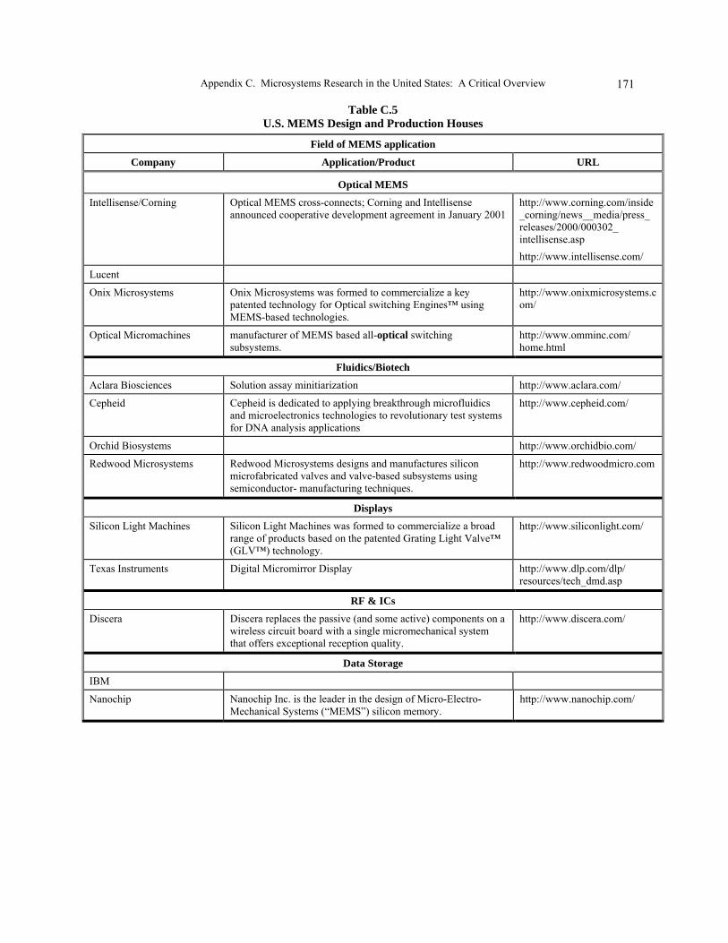
Appendix C. Microsystems Research in the United States: A Critical Overview 171
Table C.5 U.S. MEMS Design and Production Houses
Field of MEMS application
Company Application/Product URL
Optical MEMS
Intellisense/Corning Optical MEMS cross-connects; Corning and Intellisense announced cooperative development agreement in January 2001
http://www.corning.com/inside_corning/news__media/press_ releases/2000/000302_ intellisense.asp http://www.intellisense.com/
Lucent
Onix Microsystems Onix Microsystems was formed to commercialize a key patented technology for Optical switching Engines� using MEMS-based technologies.
http://www.onixmicrosystems.com/
Optical Micromachines manufacturer of MEMS based all-optical switching subsystems.
http://www.omminc.com/ home.html
Fluidics/Biotech
Aclara Biosciences Solution assay minitiarization http://www.aclara.com/
Cepheid Cepheid is dedicated to applying breakthrough microfluidics and microelectronics technologies to revolutionary test systems for DNA analysis applications
http://www.cepheid.com/
Orchid Biosystems http://www.orchidbio.com/
Redwood Microsystems Redwood Microsystems designs and manufactures silicon microfabricated valves and valve-based subsystems using semiconductor- manufacturing techniques.
http://www.redwoodmicro.com
Displays
Silicon Light Machines Silicon Light Machines was formed to commercialize a broad range of products based on the patented Grating Light Valve� (GLV�) technology.
http://www.siliconlight.com/
Texas Instruments Digital Micromirror Display http://www.dlp.com/dlp/ resources/tech_dmd.asp
RF & ICs
Discera Discera replaces the passive (and some active) components on a wireless circuit board with a single micromechanical system that offers exceptional reception quality.
http://www.discera.com/
Data Storage
IBM
Nanochip Nanochip Inc. is the leader in the design of Micro-Electro-Mechanical Systems (�MEMS�) silicon memory.
http://www.nanochip.com/
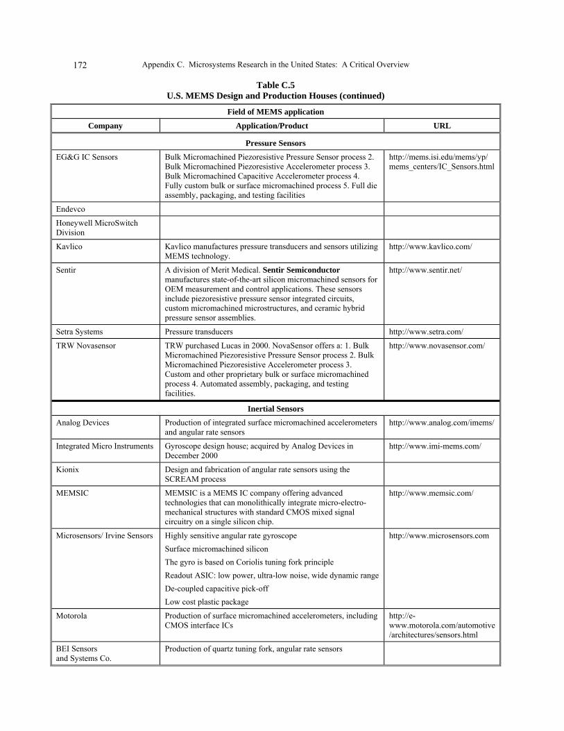
Appendix C. Microsystems Research in the United States: A Critical Overview 172
Table C.5 U.S. MEMS Design and Production Houses (continued)
Field of MEMS application
Company Application/Product URL
Pressure Sensors
EG&G IC Sensors Bulk Micromachined Piezoresistive Pressure Sensor process 2. Bulk Micromachined Piezoresistive Accelerometer process 3. Bulk Micromachined Capacitive Accelerometer process 4. Fully custom bulk or surface micromachined process 5. Full die assembly, packaging, and testing facilities
http://mems.isi.edu/mems/yp/ mems_centers/IC_Sensors.html
Endevco
Honeywell MicroSwitch Division
Kavlico Kavlico manufactures pressure transducers and sensors utilizing MEMS technology.
http://www.kavlico.com/
Sentir A division of Merit Medical. Sentir Semiconductor manufactures state-of-the-art silicon micromachined sensors for OEM measurement and control applications. These sensors include piezoresistive pressure sensor integrated circuits, custom micromachined microstructures, and ceramic hybrid pressure sensor assemblies.
http://www.sentir.net/
Setra Systems Pressure transducers http://www.setra.com/
TRW Novasensor TRW purchased Lucas in 2000. NovaSensor offers a: 1. Bulk Micromachined Piezoresistive Pressure Sensor process 2. Bulk Micromachined Piezoresistive Accelerometer process 3. Custom and other proprietary bulk or surface micromachined process 4. Automated assembly, packaging, and testing facilities.
http://www.novasensor.com/
Inertial Sensors
Analog Devices Production of integrated surface micromachined accelerometers and angular rate sensors
http://www.analog.com/imems/
Integrated Micro Instruments Gyroscope design house; acquired by Analog Devices in December 2000
http://www.imi-mems.com/
Kionix Design and fabrication of angular rate sensors using the SCREAM process
MEMSIC MEMSIC is a MEMS IC company offering advanced technologies that can monolithically integrate micro-electro-mechanical structures with standard CMOS mixed signal circuitry on a single silicon chip.
http://www.memsic.com/
Microsensors/ Irvine Sensors Highly sensitive angular rate gyroscope Surface micromachined silicon The gyro is based on Coriolis tuning fork principle Readout ASIC: low power, ultra-low noise, wide dynamic range De-coupled capacitive pick-off Low cost plastic package
http://www.microsensors.com
Motorola Production of surface micromachined accelerometers, including CMOS interface ICs
http://e-www.motorola.com/automotive/architectures/sensors.html
BEI Sensors and Systems Co.
Production of quartz tuning fork, angular rate sensors
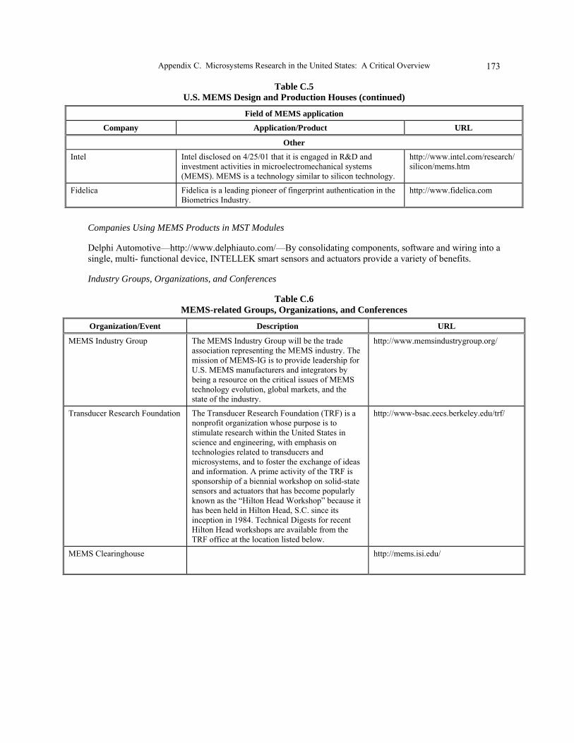
Appendix C. Microsystems Research in the United States: A Critical Overview 173
Table C.5 U.S. MEMS Design and Production Houses (continued)
Field of MEMS application
Company Application/Product URL
Other
Intel Intel disclosed on 4/25/01 that it is engaged in R&D and investment activities in microelectromechanical systems (MEMS). MEMS is a technology similar to silicon technology.
http://www.intel.com/research/silicon/mems.htm
Fidelica Fidelica is a leading pioneer of fingerprint authentication in the Biometrics Industry.
http://www.fidelica.com
Companies Using MEMS Products in MST Modules
Delphi Automotive�http://www.delphiauto.com/�By consolidating components, software and wiring into a single, multi- functional device, INTELLEK smart sensors and actuators provide a variety of benefits.
Industry Groups, Organizations, and Conferences
Table C.6 MEMS-related Groups, Organizations, and Conferences
Organization/Event Description URL
MEMS Industry Group The MEMS Industry Group will be the trade association representing the MEMS industry. The mission of MEMS-IG is to provide leadership for U.S. MEMS manufacturers and integrators by being a resource on the critical issues of MEMS technology evolution, global markets, and the state of the industry.
http://www.memsindustrygroup.org/
Transducer Research Foundation The Transducer Research Foundation (TRF) is a nonprofit organization whose purpose is to stimulate research within the United States in science and engineering, with emphasis on technologies related to transducers and microsystems, and to foster the exchange of ideas and information. A prime activity of the TRF is sponsorship of a biennial workshop on solid-state sensors and actuators that has become popularly known as the �Hilton Head Workshop� because it has been held in Hilton Head, S.C. since its inception in 1984. Technical Digests for recent Hilton Head workshops are available from the TRF office at the location listed below.
http://www-bsac.eecs.berkeley.edu/trf/
MEMS Clearinghouse http://mems.isi.edu/
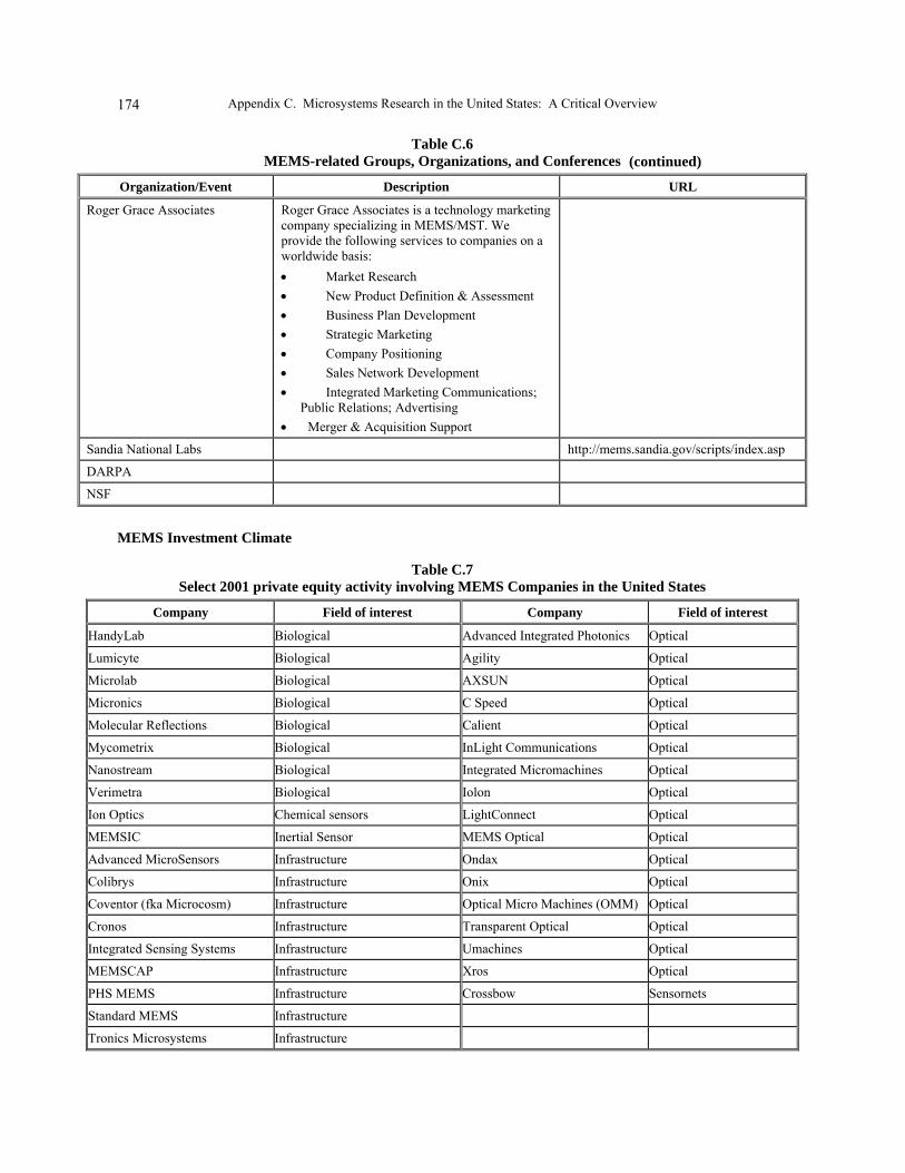
Appendix C. Microsystems Research in the United States: A Critical Overview 174
Table C.6 MEMS-related Groups, Organizations, and Conferences
Organization/Event Description URL
(continued)
Roger Grace Associates Roger Grace Associates is a technology marketing company specializing in MEMS/MST. We provide the following services to companies on a worldwide basis: • Market Research • New Product Definition & Assessment • Business Plan Development • Strategic Marketing • Company Positioning • Sales Network Development • Integrated Marketing Communications;
Public Relations; Advertising • Merger & Acquisition Support
Sandia National Labs http://mems.sandia.gov/scripts/index.asp
DARPA
NSF
MEMS Investment Climate
Table C.7 Select 2001 private equity activity involving MEMS Companies in the United States
Company Field of interest Company Field of interest
HandyLab Biological Advanced Integrated Photonics Optical
Lumicyte Biological Agility Optical
Microlab Biological AXSUN Optical
Micronics Biological C Speed Optical
Molecular Reflections Biological Calient Optical
Mycometrix Biological InLight Communications Optical
Nanostream Biological Integrated Micromachines Optical
Verimetra Biological Iolon Optical
Ion Optics Chemical sensors LightConnect Optical
MEMSIC Inertial Sensor MEMS Optical Optical
Advanced MicroSensors Infrastructure Ondax Optical
Colibrys Infrastructure Onix Optical
Coventor (fka Microcosm) Infrastructure Optical Micro Machines (OMM) Optical
Cronos Infrastructure Transparent Optical Optical
Integrated Sensing Systems Infrastructure Umachines Optical
MEMSCAP Infrastructure Xros Optical
PHS MEMS Infrastructure Crossbow Sensornets
Standard MEMS Infrastructure
Tronics Microsystems Infrastructure
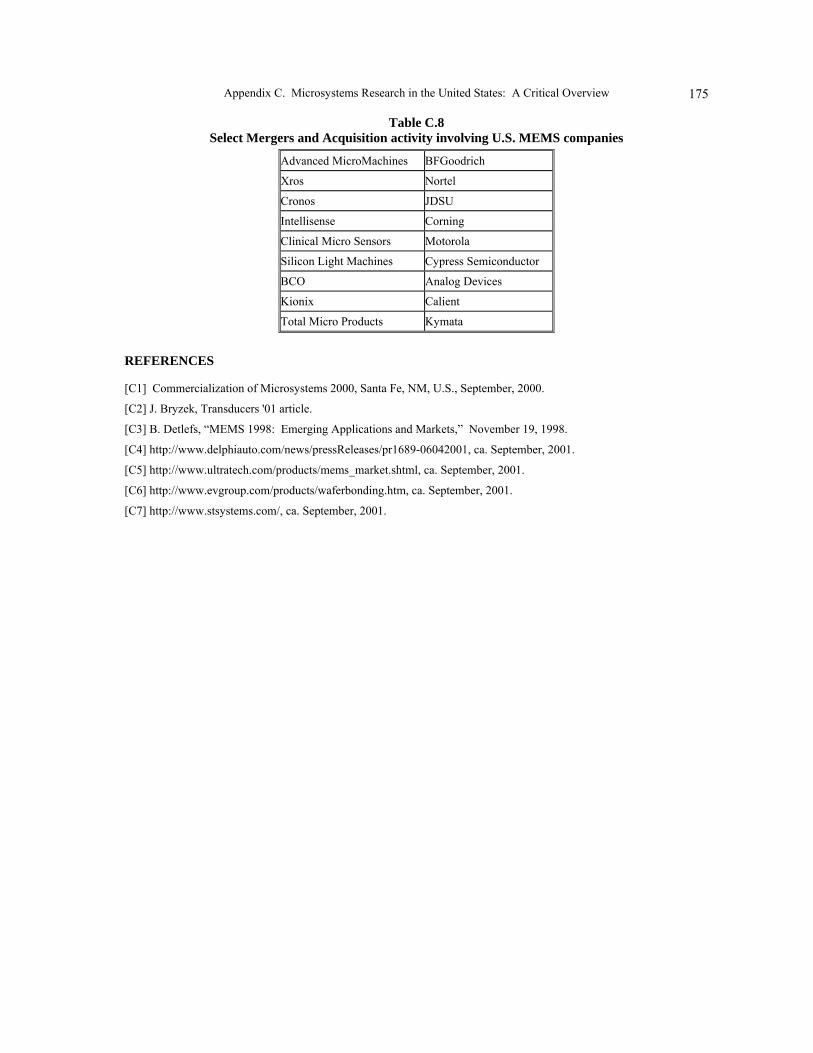
Appendix C. Microsystems Research in the United States: A Critical Overview 175
Table C.8 Select Mergers and Acquisition activity involving U.S. MEMS companies
Advanced MicroMachines BFGoodrich
Xros Nortel
Cronos JDSU
Intellisense Corning
Clinical Micro Sensors Motorola
Silicon Light Machines Cypress Semiconductor
BCO Analog Devices
Kionix Calient
Total Micro Products Kymata
REFERENCES
[C1] Commercialization of Microsystems 2000, Santa Fe, NM, U.S., September, 2000.
[C2] J. Bryzek, Transducers '01 article.
[C3] B. Detlefs, �MEMS 1998: Emerging Applications and Markets,� November 19, 1998.
[C4] http://www.delphiauto.com/news/pressReleases/pr1689-06042001, ca. September, 2001.
[C5] http://www.ultratech.com/products/mems_market.shtml, ca. September, 2001.
[C6] http://www.evgroup.com/products/waferbonding.htm, ca. September, 2001.
[C7] http://www.stsystems.com/, ca. September, 2001.
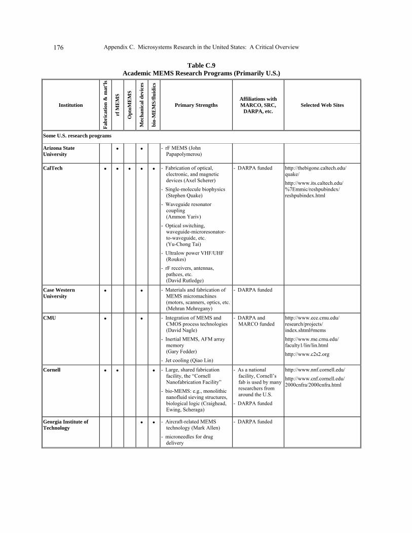
Appendix C. Microsystems Research in the United States: A Critical Overview 176
Table C.9 Academic MEMS Research Programs (Primarily U.S.)
Institution Fa
bric
atio
n &
mat
’ls
rf M
EM
S
Opt
oME
MS
Mec
hani
cal d
evic
es
bio-
ME
MS/
fluid
ics
Primary Strengths Affiliations with MARCO, SRC,
DARPA, etc. Selected Web Sites
Some U.S. research programs
Arizona State University
• • - rF MEMS (John Papapolymerou)
CalTech • • • • • - Fabrication of optical, electronic, and magnetic devices (Axel Scherer)
- Single-molecule biophysics (Stephen Quake)
- Waveguide resonator coupling (Ammon Yariv)
- Optical switching, waveguide-microresonator-to-waveguide, etc. (Yu-Chong Tai)
- Ultralow power VHF/UHF (Roukes)
- rF receivers, antennas, pathces, etc. (David Rutledge)
- DARPA funded http://thebigone.caltech.edu/ quake/
http://www.its.caltech.edu/ %7Emmic/reshpubindex/ reshpubindex.html
Case Western University
• • - Materials and fabrication of MEMS micromachines (motors, scanners, optics, etc. (Mehran Mehregany)
- DARPA funded
CMU • • - Integration of MEMS and CMOS process technologies (David Nagle)
- Inertial MEMS, AFM array memory (Gary Fedder)
- Jet cooling (Qiao Lin)
- DARPA and MARCO funded
http://www.ece.cmu.edu/ research/projects/ index.shtml#mems
http://www.me.cmu.edu/ faculty1/lin/lin.html
http://www.c2s2.org
Cornell • • • - Large, shared fabrication facility, the �Cornell Nanofabrication Facility�
- bio-MEMS: e.g., monolithic nanofluid sieving structures, biological logic (Craighead, Ewing, Scheraga)
- As a national facility, Cornell�s fab is used by many researchers from around the U.S.
- DARPA funded
http://www.nnf.cornell.edu/
http://www.cnf.cornell.edu/ 2000cnfra/2000cnfra.html
Georgia Institute of Technology
• • - Aircraft-related MEMS technology (Mark Allen)
- microneedles for drug delivery
- DARPA funded
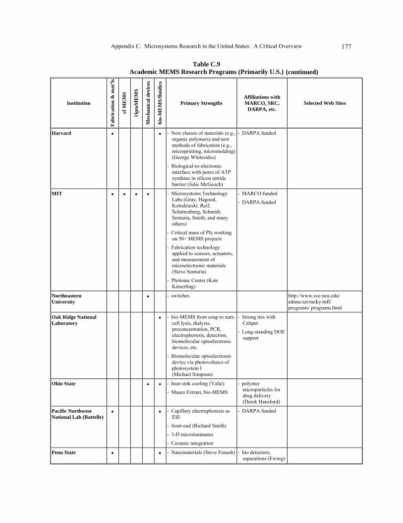
Appendix C. Microsystems Research in the United States: A Critical Overview 177
Table C.9 Academic MEMS Research Programs (Primarily U.S.)
Institution
Fabr
icat
ion
& m
at’ls
rf M
EM
S
Opt
oME
MS
Mec
hani
cal d
evic
es
bio-
ME
MS/
fluid
ics
Primary Strengths Affiliations with MARCO, SRC,
DARPA, etc. Selected Web Sites
(continued)
Harvard • • - New classes of materials (e.g., organic polymers) and new methods of fabrication (e.g., microprinting, micromolding) (George Whitesides)
- Biological-to-electronic interface with pores of ATP synthase in silicon nitride barrier (Julie McGeoch)
- DARPA funded
MIT • • • • - Microsystems Technology Labs (Gray, Hagood, Kolodzieski, Reif, Schattenburg, Schmidt, Senturia, Smith, and many others)
- Critical mass of PIs working on 50+ MEMS projects
- Fabrication technology applied to sensors, actuators, and measurement of microelectronic materials (Steve Senturia)
- Photonic Center (Kim Kimerling)
- MARCO funded
- DARPA funded
Northeastern University
• - switches http://www.ece.neu.edu/ edsnu/zavracky/mfl/ programs/ programs.html
Oak Ridge National Laboratory
• - bio-MEMS from soup to nuts: cell lysis, dialysis, preconcentration, PCR, electrophoresis, detection, biomolecular optoelectronic devices, etc.
- Biomolecular optoelectronic device via photovoltaics of photosystem I (Michael Simpson)
- Strong ties with Caliper
- Long-standing DOE support
Ohio State • • - heat-sink cooling (Vafai)
- Mauro Ferrari, bio-MEMS
- polymer microparticles for drug delivery (Derek Hansford)
Pacific Northwest National Lab (Battelle)
• • - Capillary electrophoresis as ESI
- front-end (Richard Smith)
- 3-D microlaminates
- Ceramic integration
- DARPA funded
Penn State • • - Nanomaterials (Steve Fonash) - bio detectors, separations (Ewing)
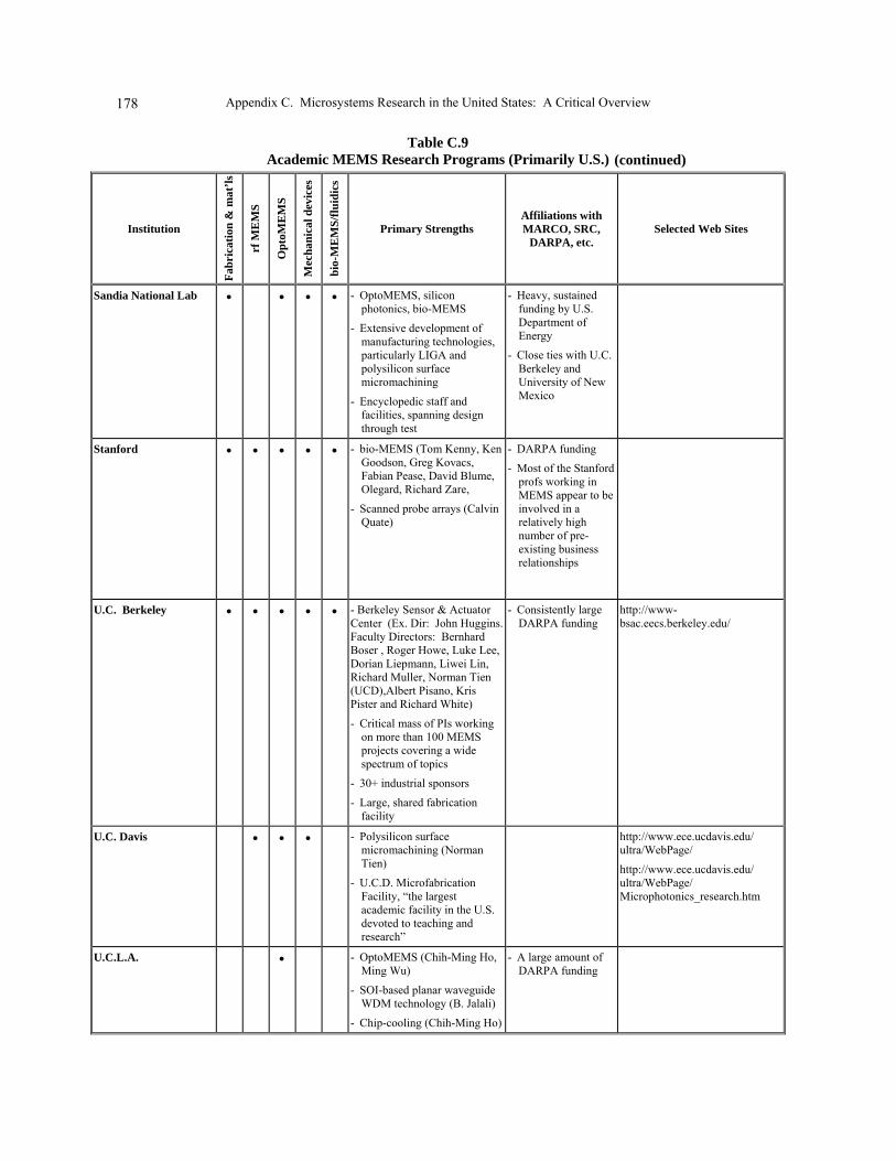
Appendix C. Microsystems Research in the United States: A Critical Overview 178
Table C.9 Academic MEMS Research Programs (Primarily U.S.)
Institution Fa
bric
atio
n &
mat
’ls
rf M
EM
S
Opt
oME
MS
Mec
hani
cal d
evic
es
bio-
ME
MS/
fluid
ics
Primary Strengths Affiliations with MARCO, SRC,
DARPA, etc. Selected Web Sites
(continued)
Sandia National Lab • • • • - OptoMEMS, silicon photonics, bio-MEMS
- Extensive development of manufacturing technologies, particularly LIGA and polysilicon surface micromachining
- Encyclopedic staff and facilities, spanning design through test
- Heavy, sustained funding by U.S. Department of Energy
- Close ties with U.C. Berkeley and University of New Mexico
Stanford • • • • • - bio-MEMS (Tom Kenny, Ken Goodson, Greg Kovacs, Fabian Pease, David Blume, Olegard, Richard Zare,
- Scanned probe arrays (Calvin Quate)
- DARPA funding
- Most of the Stanford profs working in MEMS appear to be involved in a relatively high number of pre-existing business relationships
U.C. Berkeley • • • • • - Berkeley Sensor & Actuator Center (Ex. Dir: John Huggins. Faculty Directors: Bernhard Boser , Roger Howe, Luke Lee, Dorian Liepmann, Liwei Lin, Richard Muller, Norman Tien (UCD),Albert Pisano, Kris Pister and Richard White)
- Critical mass of PIs working on more than 100 MEMS projects covering a wide spectrum of topics
- 30+ industrial sponsors
- Large, shared fabrication facility
- Consistently large DARPA funding
http://www-bsac.eecs.berkeley.edu/
U.C. Davis • • • - Polysilicon surface micromachining (Norman Tien)
- U.C.D. Microfabrication Facility, �the largest academic facility in the U.S. devoted to teaching and research�
http://www.ece.ucdavis.edu/ ultra/WebPage/
http://www.ece.ucdavis.edu/ ultra/WebPage/ Microphotonics_research.htm
U.C.L.A. • - OptoMEMS (Chih-Ming Ho, Ming Wu)
- SOI-based planar waveguide WDM technology (B. Jalali)
- Chip-cooling (Chih-Ming Ho)
- A large amount of DARPA funding
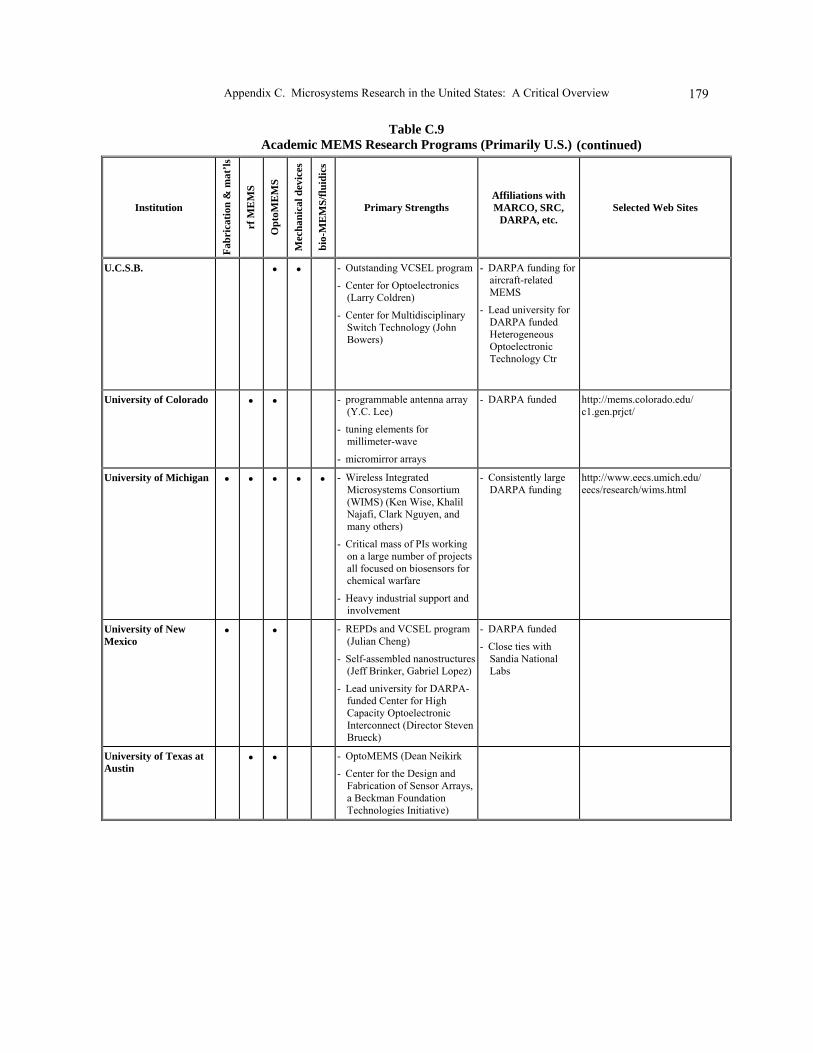
Appendix C. Microsystems Research in the United States: A Critical Overview 179
Table C.9 Academic MEMS Research Programs (Primarily U.S.)
Institution
Fabr
icat
ion
& m
at’ls
rf M
EM
S
Opt
oME
MS
Mec
hani
cal d
evic
es
bio-
ME
MS/
fluid
ics
Primary Strengths Affiliations with MARCO, SRC,
DARPA, etc. Selected Web Sites
(continued)
U.C.S.B. • • - Outstanding VCSEL program
- Center for Optoelectronics (Larry Coldren)
- Center for Multidisciplinary Switch Technology (John Bowers)
- DARPA funding for aircraft-related MEMS
- Lead university for DARPA funded Heterogeneous Optoelectronic Technology Ctr
University of Colorado • • - programmable antenna array (Y.C. Lee)
- tuning elements for millimeter-wave
- micromirror arrays
- DARPA funded http://mems.colorado.edu/ c1.gen.prjct/
University of Michigan • • • • • - Wireless Integrated Microsystems Consortium (WIMS) (Ken Wise, Khalil Najafi, Clark Nguyen, and many others)
- Critical mass of PIs working on a large number of projects all focused on biosensors for chemical warfare
- Heavy industrial support and involvement
- Consistently large DARPA funding
http://www.eecs.umich.edu/ eecs/research/wims.html
University of New Mexico
• • - REPDs and VCSEL program (Julian Cheng)
- Self-assembled nanostructures (Jeff Brinker, Gabriel Lopez)
- Lead university for DARPA-funded Center for High Capacity Optoelectronic Interconnect (Director Steven Brueck)
- DARPA funded
- Close ties with Sandia National Labs
University of Texas at Austin
• • - OptoMEMS (Dean Neikirk
- Center for the Design and Fabrication of Sensor Arrays, a Beckman Foundation Technologies Initiative)
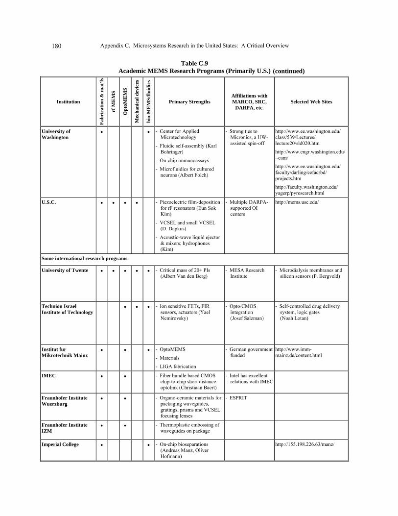
Appendix C. Microsystems Research in the United States: A Critical Overview 180
Table C.9 Academic MEMS Research Programs (Primarily U.S.)
Institution Fa
bric
atio
n &
mat
’ls
rf M
EM
S
Opt
oME
MS
Mec
hani
cal d
evic
es
bio-
ME
MS/
fluid
ics
Primary Strengths Affiliations with MARCO, SRC,
DARPA, etc. Selected Web Sites
(continued)
University of Washington
• • - Center for Applied Microtechnology
- Fluidic self-assembly (Karl Bohringer)
- On-chip immunoassays
- Microfluidics for cultured neurons (Albert Folch)
- Strong ties to Micronics, a UW-assisted spin-off
http://www.ee.washington.edu/ class/539/Lectures/ lecture20/sld020.htm
http://www.engr.washington.edu/~cam/
http://www.ee.washington.edu/ faculty/darling/eefacrbd/ projects.htm
http://faculty.washington.edu/ yagerp/pyresearch.html
U.S.C. • • • • - Piezoelectric film-deposition for rF resonators (Eun Sok Kim)
- VCSEL and small VCSEL (D. Dapkus)
- Acoustic-wave liquid ejector & mixers; hydrophones (Kim)
- Multiple DARPA-supported OI centers
http://mems.usc.edu/
Some international research programs
University of Twente • • • • • - Critical mass of 20+ PIs (Albert Van den Berg)
- MESA Research Institute
- Microdialysis membranes and silicon sensors (P. Bergveld)
Technion Israel Institute of Technology
• • • - Ion sensitive FETs, FIR sensors, actuators (Yael Nemirovsky)
- Opto/CMOS integration (Josef Salzman)
- Self-controlled drug delivery system, logic gates (Noah Lotan)
Institut fur Mikrotechnik Mainz
• • • - OptoMEMS
- Materials
- LIGA fabrication
- German government funded
http://www.imm-mainz.de/content.html
IMEC • • - Fiber bundle based CMOS chip-to-chip short distance optolink (Christiaan Baert)
- Intel has excellent relations with IMEC
Fraunhofer Institute Wuerzburg
• • - Organo-ceramic materials for packaging waveguides, gratings, prisms and VCSEL focusing lenses
- ESPRIT
Fraunhofer Institute IZM
• • - Thermoplastic embossing of waveguides on package
Imperial College • • - On-chip bioseparations (Andreas Manz, Oliver Hofmann)
http://155.198.226.63/manz/
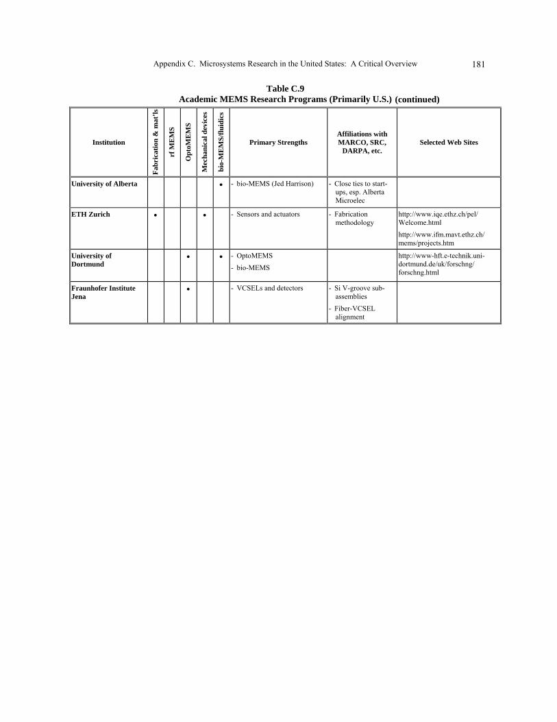
Appendix C. Microsystems Research in the United States: A Critical Overview
181
Table C.9 Academic MEMS Research Programs (Primarily U.S.)
Institution
Fabr
icat
ion
& m
at’ls
rf M
EM
S
Opt
oME
MS
Mec
hani
cal d
evic
es
bio-
ME
MS/
fluid
ics
Primary Strengths Affiliations with MARCO, SRC,
DARPA, etc. Selected Web Sites
(continued)
University of Alberta • - bio-MEMS (Jed Harrison) - Close ties to start-ups, esp. Alberta Microelec
ETH Zurich • • - Sensors and actuators - Fabrication methodology
http://www.iqe.ethz.ch/pel/ Welcome.html
http://www.ifm.mavt.ethz.ch/ mems/projects.htm
University of Dortmund
• • - OptoMEMS
- bio-MEMS
http://www-hft.e-technik.uni-dortmund.de/uk/forschng/ forschng.html
Fraunhofer Institute Jena
• - VCSELs and detectors - Si V-groove sub-assemblies
- Fiber-VCSEL alignment