app note Flatness - cyberTECHNOLOGIES€¦ · spectrometer analyzes the light intensity vs....
13
Flatness Measurement cyberTECHNOLOGIES GmbH – Georg-Kollmannsberger-Str. 3 – D-85386 Eching-Dietersheim – P: +49 89 4524666-0 Email: [email protected] - www.cybertechnologies.com
Transcript of app note Flatness - cyberTECHNOLOGIES€¦ · spectrometer analyzes the light intensity vs....

Flatness Measurement
cyberTECHNOLOGIES GmbH – Georg-Kollmannsberger-Str. 3 – D-85386 Eching-Dietersheim – P: +49 89 4524666-0
Email: [email protected] - www.cybertechnologies.com

FLATNESS MEASUREMENT
2
INTRODUCTION
With new materials and manufacturing processes engineers and developers try to reduce
tolerances and make parts smaller and more stable at the same time. Flatness and parallelism
are important parameters especially for loaded and bearing surfaces. In the electronic industry
wafer flatness and stress analysis are vital for the reliability and quality of electric devices.
Also in the aerospace and automotive industry the flatness of gaskets and bearings is
indispensable to safety and quality.
TECHNOLOGY OVERVIEW
It`s becoming more and more important to measure flatness and to detect defects ideally right
after the production process. Common methods for flatness measurements are CMM’s and
interferometer. Both methods have advantages and restrictions. A CMM is very versatile and
typically used to control all dimension of a part. The measurement process is slow and the
probe may not reach a smaller or constricted area of interest. The interferometer is a quick
method for checking flatness. Certain materials and surface reflectivity or highly contoured
parts are not suitable for the use of an interferometer. A scanning system using a high
resolution point sensor can overcome the restrictions of both of these technologies. New
confocal sensor technologies provide reliable data, independent of surface reflectivity and can
scan large surface areas fast, with up to 14 kHz data rates.
MEASUREMENT OBJECTIVE The cyberTECHNOLOGIES` CT SERIES is designed to measure flatness and other critical
dimensions on large areas. The CT 600 can handle parts or carriers up to 600 mm x 600 mm
(23.6” x 23.6”). The heart of the system is a chromatic white light sensor that takes advantage
of chromatic aberration.

FLATNESS MEASUREMENT
3
MEASUREMENT TECHNOLOGY
A very bright white light source focuses a small spot onto the sample surface with the different
wavelengths focusing on slightly different focal planes. The reflected light is collected and a
spectrometer analyzes the light intensity vs. wavelength. A height reading is generated from the
maximum intensity of a certain wavelength on the spectrometer. The sensor achieves a
resolution of 0.01 µm (10 nm).
The CT 600S massive gantry design with air bearings is moving the sensor/camera assembly
while the sample is fixed on the granite platform. This concept is ideal for precise flatness
measurement on larger parts, because the weight of the part is not affecting the accuracy of the
motion system. If the part is moved, using a traditional x-, y-stage, the weight of the part can
influence the straightness and the flatness of stage.
FLATNESS CALIBRATION
The SCAN CT Software offers the capability to calibrate the flatness of the stage for maximum
accuracy. An optical flat is used to determine and then compensate for the error of the motion
system. The CT 600S keeps an accuracy < 0.5 µm over the entire travel of 600 mm.
FLATNESS MEASUREMENT
4
SCAN SPEED
The chromatic white light sensors are available with different controller models, a LED based
controller with 2 kHz data rate, a controller using a halogen light source with 4 kHz and a 14
kHz controller based on a very bright arc lamp. With fast magnetic linear motors and 50 nm
encoder resolution, the CT SERIES can scan bidirectional. A 300 mm wafer is scanned in 3 min
and 45 second with a 1 mm step size using the 4 kHz controller.
FLATNESS MEASUREMENT ON CONTINOUS SURFACES
A good example for a continuous surface is a wafer. The procedure for this type of flatness
measurement includes only a few steps:
• Define scan area
• Scan
• Remove peaks and/or roughness
• Define measurement area
Peaks are usually caused by contamination of the surface and should be removed, because
they would affect the flatness measurement. There are 2 methods to remove peaks: A cut-off
operation or a median filter. The median filter is the preferred method. It not only removes
peaks, but can also remove other roughness effects that would affect flatness. A cut-off filter is
typically used to remove complete areas within the scan that are on a different height level and
are not relevant to the measurement at hand. Original scan showing a peak on the left side, caused by contamination
FLATNESS MEASUREMENT
5
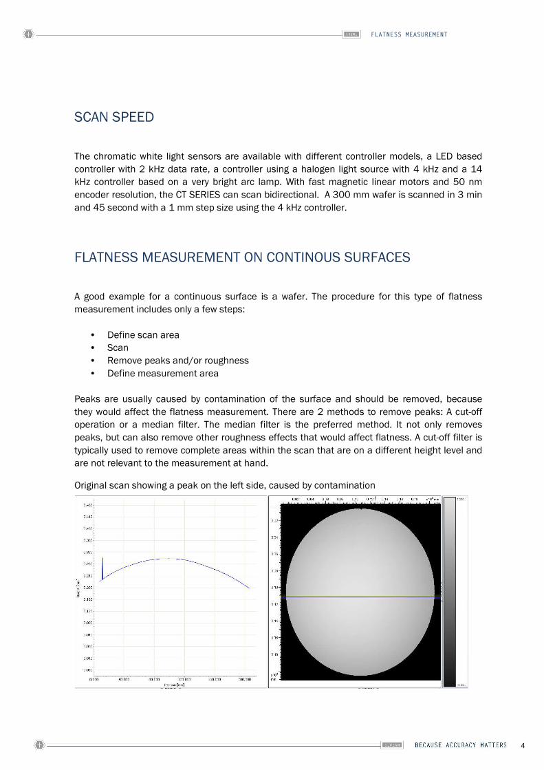
Modified scan after median filter
After removing the peaks and the roughness, the measurement cursors are placed on the scan.
For each flatness measurement it is important that a reference plane is defined. If the flatness
is measured in absolute mode, the tilt of the part is added to the flatness value. The green
reference cursor calculates a best-fit plane and the flatness is measured relative to this base
plane. The green area and the red measurement area should be located inside the area of the
wafer. The SCAN CT Software provides the ability to employ various cursor shapes. In case of
the wafer, a round cursor shape is used. Cursors are applied via simply click and drag mouse
functions.
Reference cursor Reference and measurement cursor
FLATNESS MEASUREMENT
6
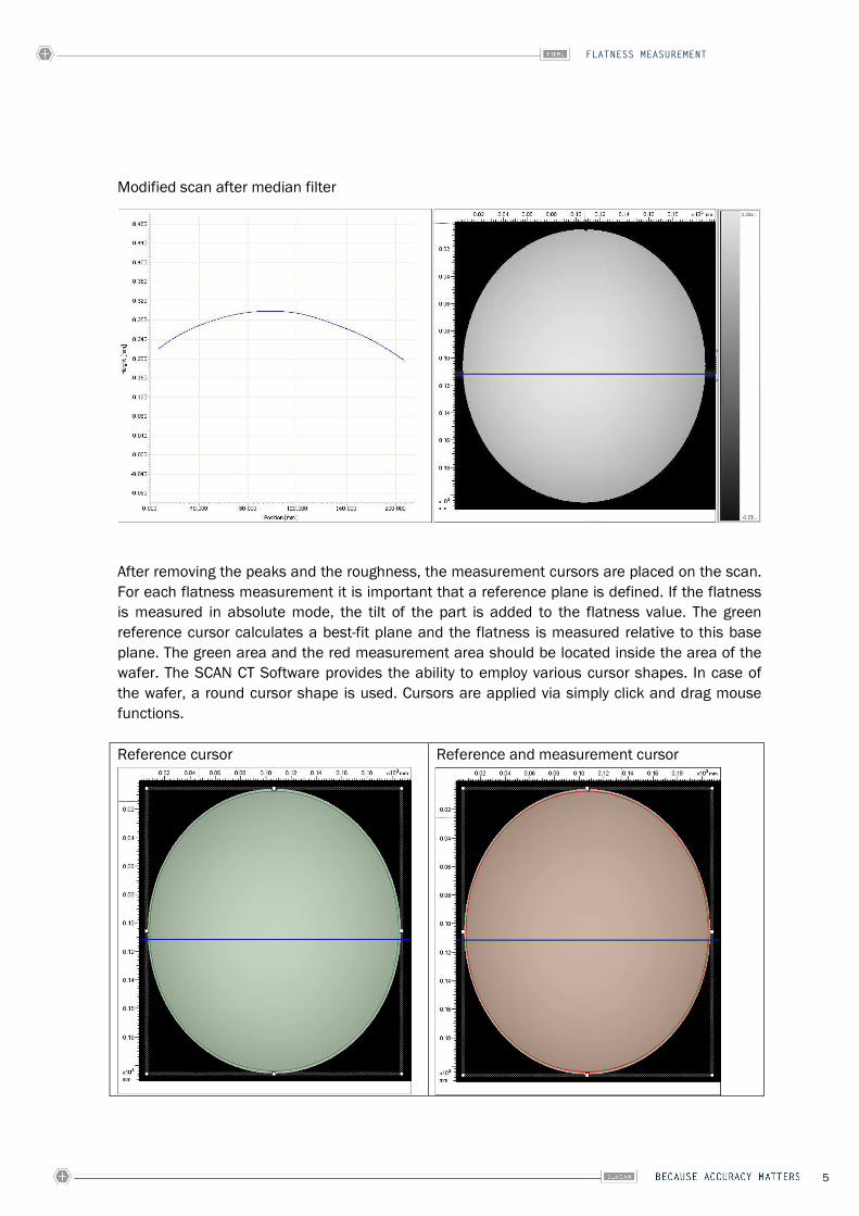
Flatness measurement showing color coded 3D map, highest and lowest point, cross-section
and histogram
3D Surface Map

FLATNESS MEASUREMENT
7
3D Contour Map
Another example is a ring shaped gaskets. These parts are used in aircraft engines, turbines
and compressors and are produced with sub-micron flatness. The gaskets are available in
different sizes and have a diameter of 500 mm or larger. To minimize the inspecting time the
cyberTECHNOLOGIES’ CT SERIES scans only the ring using circular scans not the entire area of
the gasket.
Overview Zoom

FLATNESS MEASUREMENT
8
The overview shows the entire 3D map with red dots. By clicking on the red dot the circular profile on the selected radial position is displayed. In the zoom view the density of the circular scans on the ring is more obvious. The profile shows the typical sinusoidal form that is caused by the tilt of the gasket. After normalization the tilt and the sinusoidal shape are removed.
The remaining sinus form of the profile is the real deviation from an ideally flat surface. In this example the area of interest is located in the inner part of the ring, with no surface features included. To mark this area SCAN CT allows using ring shape cursors.
3D Surface Map

FLATNESS MEASUREMENT
9
FLATNESS MEASUREMENT ON NON-CONTINUOUS SURFACES
Many mechanical parts have elevated areas or cavities and holes in the surface of interest. One
method to exclude areas that are not of interest is to use a cursor shape that simply excludes
these areas. With a few additional steps SCAN CT can remove holes and redundant areas:
• Define scan area
• Scan
• Normalize
• Delete redundant areas
• Modify edges
• Remove peaks and/or roughness
• Define measurement areas
This mechanical part shows 2 lower levels and holes within the area of interest
The first step after the scan is to normalize the raster. A few green reference cursors are placed on the surface and the software calculates the best-fit plane. “Normalizing” de-tilts the part and sets the best-fit plane to zero.

FLATNESS MEASUREMENT
10
After the normalization the lower levels are removed using a cut-off filter. Finding the correct cut-off level is now easy, because the area of interest has been set to zero. In this example SCAN CT deletes all data points which are lower than -100 µm.
In the profile on the left side it is obvious that the edges of the lower levels and the holes are still present. An edge modification filter removes the remaining data points.
Finally a median filter deletes peaks and reduces the surface roughness. After removing the edges a single measurement cursor can be used and covers the entire part.

FLATNESS MEASUREMENT
11
3D Surface
3D Contour Map

FLATNESS MEASUREMENT
12
AUTOMATION The procedures for accurate flatness measurement can be completely automated using the ASCAN Software. The operation list applies the necessary steps to the scan without user interaction.
Template
Operation List
• Fixed Cursor. Uses the template and places the green cursors.
• Normalization. De-tilts the scan and sets the reference plane to zero
• Cut-Off Filter: Removes the lower levels
• Modify Edge Regions: Removes the remaining edges left over from the cut-off filter
• Median: Deletes peaks and reduces surface roughness Since the red cursor can be sized larger as the part itself, the measurement is not sensitive lateral positioning of the sample. As long as the part is within the red box the software reports accurate flatness data. Using the ASCAN Step & Repeat function multiple parts can be placed on the stage and are measured as well as analyzed fully automatically. The data and results can simply be displayed on the screen, with indication for Go/No Go, including actual measurement results and statistics. The integrated SPC module provides the ability to control trends and access every data set individually, with user defined warn, control and specification limits. All data can also be stored or exported in a large variety of data formats and automatically imported into external production control systems.

FLATNESS MEASUREMENT
13
CONCLUSION
With their high resolution and high measurement speed, the non-contact scanning systems in
cyberTECHNOLOGIES’ CT SERIES are ideal for measuring flatness. Even parts that are as large
as 600 mm in x and y are measured with submicron accuracy.
The advanced surface analysis software makes even the most challenging measurements fast
and easy for operators, technicians or engineers alike.
For more information on cyberTECHNOLOGIES’ suite of 3D surface metrology systems please
contact us at [email protected].
cyberTECHNOLOGIES GmbH – Georg-Kollmannsberger-Str. 3 – D-85386 Eching-Dietersheim
P: +49 89 4524666-0 – F: +49 89 4524666-10 – [email protected] – www.cybertechnologies.com