ANY-RATE PRECISION CLOCKS Si5316, Si5319,Si5322, Si5323 ... · Si53xx-RM 6 Rev. 0.41 LIST OF...
156
Rev. 0.41 10/09 Copyright © 2009 by Silicon Laboratories Si53xx-RM This information applies to a product under development. Its characteristics and specifications are subject to change without notice. A NY -R ATE P RECISION C LOCKS Si5316, Si5319,Si5322, Si5323, S I 5324, Si5325, Si5326, Si5365, Si5366, Si5367, Si5368 F AMILY R EFERENCE M ANUAL
Transcript of ANY-RATE PRECISION CLOCKS Si5316, Si5319,Si5322, Si5323 ... · Si53xx-RM 6 Rev. 0.41 LIST OF...
Rev. 0.41 10/09 Copyright © 2009 by Silicon Laboratories Si53xx-RMThis information applies to a product under development. Its characteristics and specifications are subject to change without notice.
ANY-RATE PRECISION CLOCKS
Si5316, Si5319,Si5322, Si5323, SI5324, Si5325, Si5326, Si5365, Si5366, Si5367, Si5368
FAMILY REFERENCE MANUAL

Si53xx-RM
2 Rev. 0.41
Si53xx-RM
Rev. 0.41 3
TABLE OF CONTENTS
Section Page
1. Any-Rate Precision Clock Product Family Overview . . . . . . . . . . . . . . . . . . . . . . . . . . .111.1. Si5324 Introduction . . . . . . . . . . . . . . . . . . . . . . . . . . . . . . . . . . . . . . . . . . . . . . . . . .13
2. Narrowband Versus Wideband Overview . . . . . . . . . . . . . . . . . . . . . . . . . . . . . . . . . . . .143. Any-Rate Clock Family Members . . . . . . . . . . . . . . . . . . . . . . . . . . . . . . . . . . . . . . . . . . .15
3.1. Si5316 . . . . . . . . . . . . . . . . . . . . . . . . . . . . . . . . . . . . . . . . . . . . . . . . . . . . . . . . . . . .153.2. Si5319 . . . . . . . . . . . . . . . . . . . . . . . . . . . . . . . . . . . . . . . . . . . . . . . . . . . . . . . . . . . .163.3. Si5322 . . . . . . . . . . . . . . . . . . . . . . . . . . . . . . . . . . . . . . . . . . . . . . . . . . . . . . . . . . . .173.4. Si5323 . . . . . . . . . . . . . . . . . . . . . . . . . . . . . . . . . . . . . . . . . . . . . . . . . . . . . . . . . . . .183.5. Si5325 . . . . . . . . . . . . . . . . . . . . . . . . . . . . . . . . . . . . . . . . . . . . . . . . . . . . . . . . . . . .193.6. Si5326 . . . . . . . . . . . . . . . . . . . . . . . . . . . . . . . . . . . . . . . . . . . . . . . . . . . . . . . . . . . .203.7. Si5365 . . . . . . . . . . . . . . . . . . . . . . . . . . . . . . . . . . . . . . . . . . . . . . . . . . . . . . . . . . . .213.8. Si5366 . . . . . . . . . . . . . . . . . . . . . . . . . . . . . . . . . . . . . . . . . . . . . . . . . . . . . . . . . . . .223.9. Si5367 . . . . . . . . . . . . . . . . . . . . . . . . . . . . . . . . . . . . . . . . . . . . . . . . . . . . . . . . . . . .233.10. Si5368 . . . . . . . . . . . . . . . . . . . . . . . . . . . . . . . . . . . . . . . . . . . . . . . . . . . . . . . . . . .24
4. Specifications . . . . . . . . . . . . . . . . . . . . . . . . . . . . . . . . . . . . . . . . . . . . . . . . . . . . . . . . . . .255. DSPLL (All Devices) . . . . . . . . . . . . . . . . . . . . . . . . . . . . . . . . . . . . . . . . . . . . . . . . . . . . . .43
5.1. Clock Multiplication . . . . . . . . . . . . . . . . . . . . . . . . . . . . . . . . . . . . . . . . . . . . . . . . . .445.2. PLL Performance . . . . . . . . . . . . . . . . . . . . . . . . . . . . . . . . . . . . . . . . . . . . . . . . . . .45
5.2.1. Jitter Generation . . . . . . . . . . . . . . . . . . . . . . . . . . . . . . . . . . . . . . . . . . . . . . . . . . . . . . . . . . . . 455.2.2. Jitter Transfer. . . . . . . . . . . . . . . . . . . . . . . . . . . . . . . . . . . . . . . . . . . . . . . . . . . . . . . . . . . . . . . 455.2.3. Jitter Tolerance . . . . . . . . . . . . . . . . . . . . . . . . . . . . . . . . . . . . . . . . . . . . . . . . . . . . . . . . . . . . . 46
6. Pin Control Parts (Si5316, Si5322, Si5323, Si5365, Si5366) . . . . . . . . . . . . . . . . . . . . . .476.1. Clock Multiplication (Si5316, Si5322, Si5323, Si5365, Si5366) . . . . . . . . . . . . . . . .47
6.1.1. Clock Multiplication (Si5316) . . . . . . . . . . . . . . . . . . . . . . . . . . . . . . . . . . . . . . . . . . . . . . . . . . . 476.1.2. Clock Multiplication (Si5322, Si5323, Si5365, Si5366) . . . . . . . . . . . . . . . . . . . . . . . . . . . . . . . 496.1.3. CKOUT3 and CKOUT4 (Si5365 and Si5366) . . . . . . . . . . . . . . . . . . . . . . . . . . . . . . . . . . . . . . 616.1.4. Loop bandwidth (Si5316, Si5322, Si5323, Si5365, Si5366) . . . . . . . . . . . . . . . . . . . . . . . . . . . 616.1.5. Jitter Tolerance (Si5316, Si5323, Si5366) . . . . . . . . . . . . . . . . . . . . . . . . . . . . . . . . . . . . . . . . . 616.1.6. Narrowband Performance (Si5316, Si5323, Si5366). . . . . . . . . . . . . . . . . . . . . . . . . . . . . . . . . 616.1.7. Wideband Performance (Si5322 and Si5365) . . . . . . . . . . . . . . . . . . . . . . . . . . . . . . . . . . . . . . 626.1.8. Lock Detect (Si5322 and Si5365) . . . . . . . . . . . . . . . . . . . . . . . . . . . . . . . . . . . . . . . . . . . . . . . 626.1.9. Wideband Input-to-Output Skew (Si5322 and Si5365) . . . . . . . . . . . . . . . . . . . . . . . . . . . . . . . 62
6.2. PLL Self-Calibration . . . . . . . . . . . . . . . . . . . . . . . . . . . . . . . . . . . . . . . . . . . . . . . . .626.2.1. Input Clock Stability during Internal Self-Calibration (Si5316, Si5323, Si5366). . . . . . . . . . . . . 626.2.2. Self-Calibration caused by Changes in Input Frequency (Si5316, Si5322, Si5323, Si5365, Si5366) 626.2.3. Recommended Reset Guidelines (Si5316, Si5322, Si5323, Si5365, Si5366). . . . . . . . . . . . . . 626.2.4. Narrowband Input-to-Output Skew (Si5316, Si5323, Si5366) . . . . . . . . . . . . . . . . . . . . . . . . . . 62
6.3. Pin Control Input Clock Control . . . . . . . . . . . . . . . . . . . . . . . . . . . . . . . . . . . . . . . . .646.3.1. Manual Clock Selection . . . . . . . . . . . . . . . . . . . . . . . . . . . . . . . . . . . . . . . . . . . . . . . . . . . . . . . 646.3.2. Automatic Clock Selection (Si5322, Si5323, Si5365, Si5366) . . . . . . . . . . . . . . . . . . . . . . . . . . 656.3.3. Hitless Switching with Phase Build-Out (Si5323, Si5366) . . . . . . . . . . . . . . . . . . . . . . . . . . . . . 66
6.4. Digital Hold/VCO Freeze . . . . . . . . . . . . . . . . . . . . . . . . . . . . . . . . . . . . . . . . . . . . . .676.4.1. Narrowband Digital Hold (Si5316, Si5323, Si5366) . . . . . . . . . . . . . . . . . . . . . . . . . . . . . . . . . . 67
Si53xx-RM
4 Rev. 0.41
6.4.2. Recovery from Digital Hold (Si5316, Si5323, Si5366) . . . . . . . . . . . . . . . . . . . . . . . . . . . . . . . . 676.4.3. Wideband VCO Freeze (Si5322, Si5365) . . . . . . . . . . . . . . . . . . . . . . . . . . . . . . . . . . . . . . . . . 67
6.5. Frame Synchronization (Si5366) . . . . . . . . . . . . . . . . . . . . . . . . . . . . . . . . . . . . . . . .676.6. Output Phase Adjust (Si5323, Si5366) . . . . . . . . . . . . . . . . . . . . . . . . . . . . . . . . . . .68
6.6.1. FSYNC Realignment (Si5366) . . . . . . . . . . . . . . . . . . . . . . . . . . . . . . . . . . . . . . . . . . . . . . . . . . 686.6.2. Including FSYNC Inputs in Clock Selection (Si5366) . . . . . . . . . . . . . . . . . . . . . . . . . . . . . . . . 686.6.3. FS_OUT Polarity and Pulse Width Control (Si5366) . . . . . . . . . . . . . . . . . . . . . . . . . . . . . . . . . 686.6.4. Using FS_OUT as a Fifth Output Clock (Si5366) . . . . . . . . . . . . . . . . . . . . . . . . . . . . . . . . . . . 686.6.5. Disabling FS_OUT (Si5366) . . . . . . . . . . . . . . . . . . . . . . . . . . . . . . . . . . . . . . . . . . . . . . . . . . . 69
6.7. Output Clock Drivers . . . . . . . . . . . . . . . . . . . . . . . . . . . . . . . . . . . . . . . . . . . . . . . . .696.7.1. LVPECL and CMOS TQFP Output Signal Format Restrictions at 3.3 V (Si5365, Si5366) . . . . 69
6.8. PLL Bypass Mode . . . . . . . . . . . . . . . . . . . . . . . . . . . . . . . . . . . . . . . . . . . . . . . . . . .706.9. Alarms . . . . . . . . . . . . . . . . . . . . . . . . . . . . . . . . . . . . . . . . . . . . . . . . . . . . . . . . . . . .70
6.9.1. Loss-of-Signal Alarms (Si5316, Si5322, Si5323, Si5365, Si5366) . . . . . . . . . . . . . . . . . . . . . . 706.9.2. FOS Alarms (Si5365 and Si5366) . . . . . . . . . . . . . . . . . . . . . . . . . . . . . . . . . . . . . . . . . . . . . . . 706.9.3. FSYNC Align Alarm (Si5366 and CK_CONF = 1 and FRQTBL = L) . . . . . . . . . . . . . . . . . . . . . 716.9.4. C1B and C2B Alarm Outputs (Si5316, Si5322, Si5323) . . . . . . . . . . . . . . . . . . . . . . . . . . . . . . 716.9.5. C1B, C2B, C3B, and ALRMOUT Outputs (Si5365, Si5366) . . . . . . . . . . . . . . . . . . . . . . . . . . . 71
6.10. Device Reset . . . . . . . . . . . . . . . . . . . . . . . . . . . . . . . . . . . . . . . . . . . . . . . . . . . . . .726.11. DSPLLsim Configuration Software . . . . . . . . . . . . . . . . . . . . . . . . . . . . . . . . . . . . .72
7. Microprocessor Controlled Parts (Si5319, Si5325, Si5326, Si5367, Si5368) . . . . . . . . .737.1. Clock Multiplication . . . . . . . . . . . . . . . . . . . . . . . . . . . . . . . . . . . . . . . . . . . . . . . . . .73
7.1.1. Jitter Tolerance (Si5319, Si5325, Si5326, Si5367, and Si5368) . . . . . . . . . . . . . . . . . . . . . . . . 737.1.2. Wideband Mode (Si5325, Si5367) . . . . . . . . . . . . . . . . . . . . . . . . . . . . . . . . . . . . . . . . . . . . . . . 747.1.3. Narrowband Mode (Si5319, Si5326, Si5368) . . . . . . . . . . . . . . . . . . . . . . . . . . . . . . . . . . . . . . 777.1.4. Loop Bandwidth (Si5319, Si5326, Si5368) . . . . . . . . . . . . . . . . . . . . . . . . . . . . . . . . . . . . . . . . 807.1.5. Lock Detect (Si5319, Si5326, Si5368) . . . . . . . . . . . . . . . . . . . . . . . . . . . . . . . . . . . . . . . . . . . . 80
7.2. PLL Self-Calibration . . . . . . . . . . . . . . . . . . . . . . . . . . . . . . . . . . . . . . . . . . . . . . . . .817.2.1. Initiating Internal Self-Calibration . . . . . . . . . . . . . . . . . . . . . . . . . . . . . . . . . . . . . . . . . . . . . . . . 817.2.2. Input Clock Stability during Internal Self-Calibration . . . . . . . . . . . . . . . . . . . . . . . . . . . . . . . . . 817.2.3. Self-Calibration Caused by Changes in Input Frequency . . . . . . . . . . . . . . . . . . . . . . . . . . . . . 817.2.4. Narrowband Input-to-Output Skew (Si5319, Si5326, Si5368) . . . . . . . . . . . . . . . . . . . . . . . . . . 81
7.3. Input Clock Configurations (Si5367 and Si5368) . . . . . . . . . . . . . . . . . . . . . . . . . . .827.4. Microprocessor Input Clock Control . . . . . . . . . . . . . . . . . . . . . . . . . . . . . . . . . . . . .82
7.4.1. Manual Clock Selection . . . . . . . . . . . . . . . . . . . . . . . . . . . . . . . . . . . . . . . . . . . . . . . . . . . . . . . 847.4.2. Automatic Clock Selection . . . . . . . . . . . . . . . . . . . . . . . . . . . . . . . . . . . . . . . . . . . . . . . . . . . . . 847.4.3. Hitless Switching with Phase Build-Out (Si5326, Si5368) . . . . . . . . . . . . . . . . . . . . . . . . . . . . . 86
7.5. Si5319, Si5326, and Si5368 Free Run Mode . . . . . . . . . . . . . . . . . . . . . . . . . . . . . .877.5.1. Free Run Mode Programming Procedure . . . . . . . . . . . . . . . . . . . . . . . . . . . . . . . . . . . . . . . . . 877.5.2. Use of LOS_A when in Free Run Mode. . . . . . . . . . . . . . . . . . . . . . . . . . . . . . . . . . . . . . . . . . . 877.5.3. Free Run Reference Frequency Constraints . . . . . . . . . . . . . . . . . . . . . . . . . . . . . . . . . . . . . . . 887.5.4. Free Run Reference Frequency Constraints . . . . . . . . . . . . . . . . . . . . . . . . . . . . . . . . . . . . . . . 88
7.6. Digital Hold . . . . . . . . . . . . . . . . . . . . . . . . . . . . . . . . . . . . . . . . . . . . . . . . . . . . . . . .897.6.1. Narrowband Digital Hold (Si5316, Si5326, Si5368) . . . . . . . . . . . . . . . . . . . . . . . . . . . . . . . . . . 897.6.2. Recovery from Digital Hold (Si5319, Si5326, Si5368) . . . . . . . . . . . . . . . . . . . . . . . . . . . . . . . . 907.6.3. VCO Freeze (Si5319, Si5325, Si5367) . . . . . . . . . . . . . . . . . . . . . . . . . . . . . . . . . . . . . . . . . . . 91
7.7. Output Phase Adjust (Si5326, Si5368) . . . . . . . . . . . . . . . . . . . . . . . . . . . . . . . . . . .917.7.1. Coarse Skew Control (Si5326, Si5368) . . . . . . . . . . . . . . . . . . . . . . . . . . . . . . . . . . . . . . . . . . . 917.7.2. Fine Skew Control (Si5326, Si5368) . . . . . . . . . . . . . . . . . . . . . . . . . . . . . . . . . . . . . . . . . . . . . 927.7.3. Independent Skew (Si5326, Si5368) . . . . . . . . . . . . . . . . . . . . . . . . . . . . . . . . . . . . . . . . . . . . . 927.7.4. Output-to-output Skew (Si5326, Si5368) . . . . . . . . . . . . . . . . . . . . . . . . . . . . . . . . . . . . . . . . . . 92
Si53xx-RM
Rev. 0.41 5
7.8. Frame Synchronization Realignment (Si5368 and CK_CONFIG_REG = 1) . . . . . . .927.8.1. FSYNC Realignment (Si5368) . . . . . . . . . . . . . . . . . . . . . . . . . . . . . . . . . . . . . . . . . . . . . . . . . . 947.8.2. FSYNC Skew Control . . . . . . . . . . . . . . . . . . . . . . . . . . . . . . . . . . . . . . . . . . . . . . . . . . . . . . . . 957.8.3. Including FSYNC Inputs in Clock Selection (Si5368) . . . . . . . . . . . . . . . . . . . . . . . . . . . . . . . . 957.8.4. FS_OUT Polarity and Pulse Width Control (Si5368) . . . . . . . . . . . . . . . . . . . . . . . . . . . . . . . . . 967.8.5. Using FS_OUT as a Fifth Output Clock (Si5368) . . . . . . . . . . . . . . . . . . . . . . . . . . . . . . . . . . . 96
7.9. Output Clock Drivers (Si5319, Si5325, Si5326, Si5367, Si5368) . . . . . . . . . . . . . . .977.9.1. Disabling CKOUTn. . . . . . . . . . . . . . . . . . . . . . . . . . . . . . . . . . . . . . . . . . . . . . . . . . . . . . . . . . . 977.9.2. LVPECL TQFP Output Signal Format Restrictions at 3.3 V (Si536, Si5368) . . . . . . . . . . . . . . 97
7.10. PLL Bypass Mode (Si5319, Si5325, Si5326, Si5367, Si5368) . . . . . . . . . . . . . . . .977.11. Alarms (Si5319, Si5325, Si5326, Si5367, Si5368) . . . . . . . . . . . . . . . . . . . . . . . . .98
7.11.1. Loss-of-Signal Alarms (Si5319, Si5325, Si5326, Si5367, Si5368) . . . . . . . . . . . . . . . . . . . . . 987.11.2. FOS Algorithm (Si5326, Si5368) . . . . . . . . . . . . . . . . . . . . . . . . . . . . . . . . . . . . . . . . . . . . . . . 997.11.3. C1B, C2B (Si5319, Si5325, Si5326) . . . . . . . . . . . . . . . . . . . . . . . . . . . . . . . . . . . . . . . . . . . 1017.11.4. C1B, C2B, C3B, ALRMOUT (Si5367, Si5368 [CK_CONFIG_REG = 0]). . . . . . . . . . . . . . . . 1017.11.5. C1B, C2B, C3B, ALRMOUT (Si5368 [CK_CONFIG_REG = 1]) . . . . . . . . . . . . . . . . . . . . . . 1027.11.6. LOS Algorithm for Reference Clock Input (Si5326, Si5368) . . . . . . . . . . . . . . . . . . . . . . . . . 1027.11.7. LOL (Si5319, Si5326, Si5368) . . . . . . . . . . . . . . . . . . . . . . . . . . . . . . . . . . . . . . . . . . . . . . . . 1027.11.8. Device Interrupts . . . . . . . . . . . . . . . . . . . . . . . . . . . . . . . . . . . . . . . . . . . . . . . . . . . . . . . . . . 103
7.12. Device Reset . . . . . . . . . . . . . . . . . . . . . . . . . . . . . . . . . . . . . . . . . . . . . . . . . . . . .1037.13. I2C Serial Microprocessor Interface (Si5325, Si5326, Si5367, Si5368) . . . . . . . .1037.14. Serial Microprocessor Interface (SPI) . . . . . . . . . . . . . . . . . . . . . . . . . . . . . . . . . .105
7.14.1. Default Device Configuration . . . . . . . . . . . . . . . . . . . . . . . . . . . . . . . . . . . . . . . . . . . . . . . . . 1067.15. Register Descriptions . . . . . . . . . . . . . . . . . . . . . . . . . . . . . . . . . . . . . . . . . . . . . .1067.16. DSPLLsim Configuration Software . . . . . . . . . . . . . . . . . . . . . . . . . . . . . . . . . . . .106
8. High-Speed I/O . . . . . . . . . . . . . . . . . . . . . . . . . . . . . . . . . . . . . . . . . . . . . . . . . . . . . . . . .1078.1. Input Clock Buffers . . . . . . . . . . . . . . . . . . . . . . . . . . . . . . . . . . . . . . . . . . . . . . . . .1078.2. Output Clock Drivers . . . . . . . . . . . . . . . . . . . . . . . . . . . . . . . . . . . . . . . . . . . . . . . .109
8.2.1. LVPECL TQFP Output Signal Format Restrictions at 3.3 V (Si5367, Si5368) . . . . . . . . . . . . 1098.3. Crystal/Reference Clock Interfaces (Si5316, Si5319, Si5323, Si5326, Si5366, & Si5368) . . . . . . . . . . . . . . . . . . . . . . . . . . . . . . . . . . . . . . . . . . . . . . . . . . . . . . . . . . . . . .1118.4. Three-Level (3L) Input Pins (No External Resistors) . . . . . . . . . . . . . . . . . . . . . . .1138.5. Three-Level (3L) Input Pins (With External Resistors) . . . . . . . . . . . . . . . . . . . . . .114
9. Power Supply . . . . . . . . . . . . . . . . . . . . . . . . . . . . . . . . . . . . . . . . . . . . . . . . . . . . . . . . . .11510. Packages and Ordering Guide . . . . . . . . . . . . . . . . . . . . . . . . . . . . . . . . . . . . . . . . . . .116Appendix A—Narrowband References . . . . . . . . . . . . . . . . . . . . . . . . . . . . . . . . . . . . . . .117Appendix B—Frequency Plans and Jitter Performance (Si5316, Si5319, Si5323, Si5326, Si5366, Si5368) . . . . . . . . . . . . . . . . . . . . . . . . . . . . . . . .119Appendix C—Typical Phase Noise Plots . . . . . . . . . . . . . . . . . . . . . . . . . . . . . . . . . . . . . .124Appendix D—Alarm Structure . . . . . . . . . . . . . . . . . . . . . . . . . . . . . . . . . . . . . . . . . . . . . . .138Appendix E—Internal Pullup, Pulldown by Pin . . . . . . . . . . . . . . . . . . . . . . . . . . . . . . . . .141Appendix F—Typical Performance . . . . . . . . . . . . . . . . . . . . . . . . . . . . . . . . . . . . . . . . . . .146Document Change List . . . . . . . . . . . . . . . . . . . . . . . . . . . . . . . . . . . . . . . . . . . . . . . . . . . .154Contact Information . . . . . . . . . . . . . . . . . . . . . . . . . . . . . . . . . . . . . . . . . . . . . . . . . . . . . . .156
Si53xx-RM
6 Rev. 0.41
L IST OF FIGURES
1. Any-Rate Precision Clock Product Family Overview2. Narrowband Versus Wideband Overview3. Any-Rate Clock Family MembersFigure 1. Si5316 Jitter Attenuator Block Diagram . . . . . . . . . . . . . . . . . . . . . . . . . . . . . . . . . . 14Figure 2. Si5319 Clock Multiplier Block Diagram . . . . . . . . . . . . . . . . . . . . . . . . . . . . . . . . . . .15Figure 3. Si5322 Clock Multiplier Block Diagram . . . . . . . . . . . . . . . . . . . . . . . . . . . . . . . . . . 16Figure 4. Si5323 Clock Multiplier and Jitter Attenuator Block Diagram. . . . . . . . . . . . . . . . . . 17Figure 5. Si5325 Clock Multiplier Block Diagram . . . . . . . . . . . . . . . . . . . . . . . . . . . . . . . . . . 18Figure 6. Si5326 Clock Multiplier and Jitter Attenuator Block Diagram. . . . . . . . . . . . . . . . . . 19Figure 7. Si5365 Clock Multiplier Block Diagram . . . . . . . . . . . . . . . . . . . . . . . . . . . . . . . . . . 20Figure 8. Si5366 Clock Multiplier and Jitter Attenuator Block Diagram. . . . . . . . . . . . . . . . . . 21Figure 9. Si5367 Clock Multiplier Block Diagram . . . . . . . . . . . . . . . . . . . . . . . . . . . . . . . . . . 22Figure 10. Si5368 Clock Multiplier and Jitter Attenuator Block Diagram. . . . . . . . . . . . . . . . . 234. SpecificationsFigure 11. Differential Voltage Characteristics . . . . . . . . . . . . . . . . . . . . . . . . . . . . . . . . . . . . 24Figure 12. Rise/Fall Time Characteristics . . . . . . . . . . . . . . . . . . . . . . . . . . . . . . . . . . . . . . . . 24Figure 13. Frame Synchronization Timing in Level Sensitive Mode . . . . . . . . . . . . . . . . . . . . 31Figure 14. Frame Synchronization Timing in One-shot Mode. . . . . . . . . . . . . . . . . . . . . . . . . 31Figure 15. SPI Timing Diagram. . . . . . . . . . . . . . . . . . . . . . . . . . . . . . . . . . . . . . . . . . . . . . . . 415. DSPLL (All Devices)Figure 16. Any-Rate Precision Clock DSPLL Block Diagram . . . . . . . . . . . . . . . . . . . . . . . . . 42Figure 17. Clock Multiplication Circuit . . . . . . . . . . . . . . . . . . . . . . . . . . . . . . . . . . . . . . . . . . . 43Figure 18. PLL Jitter Transfer Mask/Template . . . . . . . . . . . . . . . . . . . . . . . . . . . . . . . . . . . . 44Figure 19. Jitter Tolerance Mask/Template. . . . . . . . . . . . . . . . . . . . . . . . . . . . . . . . . . . . . . . 456. Pin Control Parts (Si5316, Si5322, Si5323, Si5365, Si5366)Figure 20. Si5316 Divisor Ratios. . . . . . . . . . . . . . . . . . . . . . . . . . . . . . . . . . . . . . . . . . . . . . . 477. Microprocessor Controlled Parts (Si5319, Si5325, Si5326, Si5367, Si5368)Figure 21. Wideband PLL Divider Settings (Si5325, Si5367) . . . . . . . . . . . . . . . . . . . . . . . . . 73Figure 22. Narrowband PLL Divider Settings (Si5319, Si5326, Si5368) . . . . . . . . . . . . . . . . . 76Figure 23. Si5325 and Si5326 Input Clock Selection . . . . . . . . . . . . . . . . . . . . . . . . . . . . . . . 81Figure 24. Si5367 and Si5368 Input Clock Selection . . . . . . . . . . . . . . . . . . . . . . . . . . . . . . . 82Figure 25. Free Run Mode Block Diagram . . . . . . . . . . . . . . . . . . . . . . . . . . . . . . . . . . . . . . . .86Figure 26. Parameters in History Value of M . . . . . . . . . . . . . . . . . . . . . . . . . . . . . . . . . . . . . 88Figure 27. Frame Sync Frequencies . . . . . . . . . . . . . . . . . . . . . . . . . . . . . . . . . . . . . . . . . . . . 92Figure 28. FOS Compare . . . . . . . . . . . . . . . . . . . . . . . . . . . . . . . . . . . . . . . . . . . . . . . . . . . . 99Figure 29. I2C Command Format . . . . . . . . . . . . . . . . . . . . . . . . . . . . . . . . . . . . . . . . . . . . . 103Figure 30. SPI Write/Set Address Command . . . . . . . . . . . . . . . . . . . . . . . . . . . . . . . . . . . . 105Figure 31. SPI Read Command . . . . . . . . . . . . . . . . . . . . . . . . . . . . . . . . . . . . . . . . . . . . . . 1058. High-Speed I/OFigure 32. Differential LVPECL Termination . . . . . . . . . . . . . . . . . . . . . . . . . . . . . . . . . . . . . 106Figure 33. Single-Ended LVPECL Termination. . . . . . . . . . . . . . . . . . . . . . . . . . . . . . . . . . . 106Figure 34. CML/LVDS Termination (1.8, 2.5, 3.3 V) . . . . . . . . . . . . . . . . . . . . . . . . . . . . . . . 107Figure 35. CMOS Termination (1.8, 2.5, 3.3 V). . . . . . . . . . . . . . . . . . . . . . . . . . . . . . . . . . . 107
Si53xx-RM
Rev. 0.41 7
Figure 36. Typical Output Circuit (Not CMOS) . . . . . . . . . . . . . . . . . . . . . . . . . . . . . . . . . . . 108Figure 37. Typical CMOS Output Circuit (Tie CKOUTn+ and CKOUTn– Together) . . . . . . . 108Figure 38. Differential Input Clock . . . . . . . . . . . . . . . . . . . . . . . . . . . . . . . . . . . . . . . . . . . . . 109Figure 39. CKOUT Structure . . . . . . . . . . . . . . . . . . . . . . . . . . . . . . . . . . . . . . . . . . . . . . . . . 109Figure 40. CMOS External Reference Circuit . . . . . . . . . . . . . . . . . . . . . . . . . . . . . . . . . . . . 110Figure 41. Sinewave External Clock Circuit . . . . . . . . . . . . . . . . . . . . . . . . . . . . . . . . . . . . . 110Figure 42. Differential External Reference Input Example . . . . . . . . . . . . . . . . . . . . . . . . . . .111Figure 43. Three Level Input Pins . . . . . . . . . . . . . . . . . . . . . . . . . . . . . . . . . . . . . . . . . . . . . 112Figure 44. Three Level Input Pins . . . . . . . . . . . . . . . . . . . . . . . . . . . . . . . . . . . . . . . . . . . . . 1139. Power SupplyFigure 45. Typical Power Supply Bypass Network (TQFP Package) . . . . . . . . . . . . . . . . . . 114Figure 46. Typical Power Supply Bypass Network (QFN Package) . . . . . . . . . . . . . . . . . . . 11410. Packages and Ordering GuideAppendix A—Narrowband ReferencesFigure 47. Typical Reference Jitter Transfer Function . . . . . . . . . . . . . . . . . . . . . . . . . . . . . 117Appendix B—Frequency Plans and Jitter Performance (Si5316, Si5319, Si5323, Si5326, Si5366, Si5368)Figure 48. Jitter vs. f3 . . . . . . . . . . . . . . . . . . . . . . . . . . . . . . . . . . . . . . . . . . . . . . . . . . . . . . 118Figure 49. Jitter vs. f3 with FPGA . . . . . . . . . . . . . . . . . . . . . . . . . . . . . . . . . . . . . . . . . . . . . 119Figure 50. Reference vs. Output Frequency . . . . . . . . . . . . . . . . . . . . . . . . . . . . . . . . . . . . . 120Figure 51. Jitter vs. Reference Frequency (1 of 2) . . . . . . . . . . . . . . . . . . . . . . . . . . . . . . . . 121Figure 52. Jitter vs. Reference Frequency (2 of 2) . . . . . . . . . . . . . . . . . . . . . . . . . . . . . . . . 122Appendix C—Typical Phase Noise PlotsAppendix D—Alarm StructureFigure 53. Si5326 Alarm Diagram. . . . . . . . . . . . . . . . . . . . . . . . . . . . . . . . . . . . . . . . . . . . . 137Figure 54. Si5368 Alarm Diagram (1 of 2). . . . . . . . . . . . . . . . . . . . . . . . . . . . . . . . . . . . . . . 138Figure 55. Si5368 Alarm Diagram (2 of 2). . . . . . . . . . . . . . . . . . . . . . . . . . . . . . . . . . . . . . . 139Appendix E—Internal Pullup, Pulldown by PinAppendix F—Typical PerformanceDocument Change ListContact Information
Si53xx-RM
8 Rev. 0.41
L IST OF TABLES
1. Any-Rate Precision Clock Product Family OverviewTable 1. Product Selection Guide . . . . . . . . . . . . . . . . . . . . . . . . . . . . . . . . . . . . . . . . . . . . . . 112. Narrowband Versus Wideband Overview3. Any-Rate Clock Family Members4. SpecificationsTable 2. Recommended Operating Conditions1 . . . . . . . . . . . . . . . . . . . . . . . . . . . . . . . . . . . 24Table 3. DC Characteristics—All Parts (Current draw is independent of supply voltage). . . . 25Table 4. DC Characteristics—Microprocessor Devices (Si5319, Si5325, Si5326, Si5367, Si5368) . . . . . . . . . . . . . . . . . . . . . . . . . . . . . . . . . . . . . . . . . . . . . . . . . . . . . . . . . . . . . . . . . . . . . . . . .30Table 5. DC Characteristics—Narrowband Devices (Si5316, Si5319, Si5323, Si5326, Si5366, Si5368) . . . . . . . . . . . . . . . . . . . . . . . . . . . . . . . . . . . . . . . . . . . . . . . . . . . . . . . . . . . . . . . . . . 30Table 6. AC Characteristics—All Parts . . . . . . . . . . . . . . . . . . . . . . . . . . . . . . . . . . . . . . . . . . 32Table 7. Jitter Generation (Si5316, Si5319, Si5323, Si5326, Si5366, Si5368) . . . . . . . . . . . . 39Table 8. Jitter Generation (Si5322, Si5325, Si5365, Si5367) . . . . . . . . . . . . . . . . . . . . . . . . . 40Table 9. SPI Specifications (Si5319, Si5325, Si5326, Si5367, and Si5368) . . . . . . . . . . . . . . 40Table 10. Thermal Characteristics . . . . . . . . . . . . . . . . . . . . . . . . . . . . . . . . . . . . . . . . . . . . . 415. DSPLL (All Devices)6. Pin Control Parts (Si5316, Si5322, Si5323, Si5365, Si5366)Table 11. Si5316, Si5322, Si5323, Si5365 and Si5366 Key Features . . . . . . . . . . . . . . . . . . 46Table 12. Frequency Settings . . . . . . . . . . . . . . . . . . . . . . . . . . . . . . . . . . . . . . . . . . . . . . . . . 46Table 13. Input Divider Settings . . . . . . . . . . . . . . . . . . . . . . . . . . . . . . . . . . . . . . . . . . . . . . . 47Table 14. Si5316 BW Values . . . . . . . . . . . . . . . . . . . . . . . . . . . . . . . . . . . . . . . . . . . . . . . . . 47Table 15. SONET Clock Multiplication Settings (FRQTBL=L) . . . . . . . . . . . . . . . . . . . . . . . . 48Table 16. Datacom Clock Multiplication Settings (FRQTBL = M, CK_CONF=0) . . . . . . . . . . 53Table 17. SONET to Datacom Clock Multiplication Settings (FRQTBL = H, CK_CONF = 0) . 57Table 18. Clock Output Divider Control (DIV34) . . . . . . . . . . . . . . . . . . . . . . . . . . . . . . . . . . . 60Table 19. Si5316, Si5322, and Si5323 Pins and Reset . . . . . . . . . . . . . . . . . . . . . . . . . . . . . 62Table 20. Si5365 and Si5366 Pins and Reset. . . . . . . . . . . . . . . . . . . . . . . . . . . . . . . . . . . . . 62Table 21. Manual Input Clock Selection (Si5316, Si5322, Si5323), AUTOSEL = L . . . . . . . . 63Table 22. Manual Input Clock Selection (Si5365, Si5366), AUTOSEL = L . . . . . . . . . . . . . . . 63Table 23. Automatic/Manual Clock Selection . . . . . . . . . . . . . . . . . . . . . . . . . . . . . . . . . . . . . 64Table 24. Clock Active Indicators (AUTOSEL = M or H) (Si5322 and Si5323) . . . . . . . . . . . . 64Table 25. Clock Active Indicators (AUTOSEL = M or H) (Si5365 and Si5367) . . . . . . . . . . . . 64Table 26. Input Clock Priority for Auto Switching (Si5322, Si5323) . . . . . . . . . . . . . . . . . . . . 64Table 27. Input Clock Priority for Auto Switching (Si5365, Si5366) . . . . . . . . . . . . . . . . . . . . 65Table 28. FS_OUT Disable Control (DBLFS) . . . . . . . . . . . . . . . . . . . . . . . . . . . . . . . . . . . . . 68Table 29. Output Signal Format Selection (SFOUT). . . . . . . . . . . . . . . . . . . . . . . . . . . . . . . . 68Table 30. DSBL2/BYPASS Pin Settings . . . . . . . . . . . . . . . . . . . . . . . . . . . . . . . . . . . . . . . . . 69Table 31. Frequency Offset Control (FOS_CTL). . . . . . . . . . . . . . . . . . . . . . . . . . . . . . . . . . . 70Table 32. Alarm Output Logic Equations. . . . . . . . . . . . . . . . . . . . . . . . . . . . . . . . . . . . . . . . . 70Table 33. Lock Detect Retrigger Time. . . . . . . . . . . . . . . . . . . . . . . . . . . . . . . . . . . . . . . . . . . 717. Microprocessor Controlled Parts (Si5319, Si5325, Si5326, Si5367, Si5368)Table 34. Si5325, Si5326, Si5367 and Si5368 Key Features . . . . . . . . . . . . . . . . . . . . . . . . . 72
Si53xx-RM
Rev. 0.41 9
Table 35. Device Control Modes. . . . . . . . . . . . . . . . . . . . . . . . . . . . . . . . . . . . . . . . . . . . . . . 72Table 36. Common Divider Settings (Wideband/µP Control Mode - Si5325 and Si5367) . . . 74Table 37. Common Loop Bandwidth (MHz) (Si5325 and Si5367) . . . . . . . . . . . . . . . . . . . . . 75Table 38. Narrowband Frequency Limits . . . . . . . . . . . . . . . . . . . . . . . . . . . . . . . . . . . . . . . . 77Table 39. Dividers and Limits . . . . . . . . . . . . . . . . . . . . . . . . . . . . . . . . . . . . . . . . . . . . . . . . . 77Table 40. Common Divider Settings (Si5319, Si5326, Si5368). . . . . . . . . . . . . . . . . . . . . . . . 78Table 41. Common Loop Bandwidth Settings (Si5319, Si5326 and Si5368) . . . . . . . . . . . . . 79Table 42. Input Clock Configurations . . . . . . . . . . . . . . . . . . . . . . . . . . . . . . . . . . . . . . . . . . . 81Table 43. Manual Input Clock Selection (Si5367, Si5368) . . . . . . . . . . . . . . . . . . . . . . . . . . . 83Table 44. Manual Input Clock Selection (Si5325, Si5326) . . . . . . . . . . . . . . . . . . . . . . . . . . . 83Table 45. Automatic/Manual Clock Selection . . . . . . . . . . . . . . . . . . . . . . . . . . . . . . . . . . . . . 83Table 46. Input Clock Priority for Auto Switching in µP Control Mode . . . . . . . . . . . . . . . . . . 84Table 47. Digital Hold History Delay . . . . . . . . . . . . . . . . . . . . . . . . . . . . . . . . . . . . . . . . . . . . 88Table 48. Digital Hold History Averaging Time . . . . . . . . . . . . . . . . . . . . . . . . . . . . . . . . . . . . 89Table 49. CKIN3/CKIN4 Frequency Selection (CK_CONF = 1) . . . . . . . . . . . . . . . . . . . . . . . 92Table 50. Common NC5 Divider Settings . . . . . . . . . . . . . . . . . . . . . . . . . . . . . . . . . . . . . . . . 93Table 51. Alignment Alarm Trigger Threshold. . . . . . . . . . . . . . . . . . . . . . . . . . . . . . . . . . . . . 94Table 52. Output Signal Format Selection . . . . . . . . . . . . . . . . . . . . . . . . . . . . . . . . . . . . . . . 96Table 53. Loss-of-Signal Validation Times . . . . . . . . . . . . . . . . . . . . . . . . . . . . . . . . . . . . . . . 97Table 54. Loss-of-Signal Registers . . . . . . . . . . . . . . . . . . . . . . . . . . . . . . . . . . . . . . . . . . . . . 97Table 55. FOS Reference Clock Selection . . . . . . . . . . . . . . . . . . . . . . . . . . . . . . . . . . . . . . . 99Table 56. CLKnRATE Registers . . . . . . . . . . . . . . . . . . . . . . . . . . . . . . . . . . . . . . . . . . . . . . . 99Table 57. Alarm Output Logic Equations (Si5367 and Si5368 [CONFIG_REG = 0]) . . . . . . 100Table 58. Alarm Output Logic Equations [Si5368 and CKCONFIG_REG = 1] . . . . . . . . . . . 101Table 59. Lock Detect Retrigger Time (LOCKT) . . . . . . . . . . . . . . . . . . . . . . . . . . . . . . . . . . 102Table 60. SPI Command Format. . . . . . . . . . . . . . . . . . . . . . . . . . . . . . . . . . . . . . . . . . . . . . 1048. High-Speed I/OTable 61. Output Driver Configuration. . . . . . . . . . . . . . . . . . . . . . . . . . . . . . . . . . . . . . . . . . 108Table 62. Disabling Unused Output Driver . . . . . . . . . . . . . . . . . . . . . . . . . . . . . . . . . . . . . . 1099. Power Supply10. Packages and Ordering GuideAppendix A—Narrowband ReferencesTable 63. Approved Crystals . . . . . . . . . . . . . . . . . . . . . . . . . . . . . . . . . . . . . . . . . . . . . . . . . 116Table 64. XA/XB Reference Sources and Frequencies . . . . . . . . . . . . . . . . . . . . . . . . . . . . 116Appendix B—Frequency Plans and Jitter Performance (Si5316, Si5319, Si5323, Si5326, Si5366, Si5368)Table 65. Jitter Values for Figure 49 . . . . . . . . . . . . . . . . . . . . . . . . . . . . . . . . . . . . . . . . . . . 119Table 66. Jitter Values for Figure 50 . . . . . . . . . . . . . . . . . . . . . . . . . . . . . . . . . . . . . . . . . . . 120Appendix C—Typical Phase Noise PlotsAppendix D—Alarm StructureAppendix E—Internal Pullup, Pulldown by PinTable 67. Si5316 Pullup/down. . . . . . . . . . . . . . . . . . . . . . . . . . . . . . . . . . . . . . . . . . . . . . . . 140Table 68. Si5322 Pullup/down. . . . . . . . . . . . . . . . . . . . . . . . . . . . . . . . . . . . . . . . . . . . . . . . 140Table 69. Si5323 Pullup/down. . . . . . . . . . . . . . . . . . . . . . . . . . . . . . . . . . . . . . . . . . . . . . . . 141Table 70. Si5325 Pullup/down. . . . . . . . . . . . . . . . . . . . . . . . . . . . . . . . . . . . . . . . . . . . . . . . 141Table 71. Si5326 Pullup/down. . . . . . . . . . . . . . . . . . . . . . . . . . . . . . . . . . . . . . . . . . . . . . . . 142
Si53xx-RM
10 Rev. 0.41
Table 72. Si5365 Pullup/down. . . . . . . . . . . . . . . . . . . . . . . . . . . . . . . . . . . . . . . . . . . . . . . . 142Table 73. Si5366 Pullup/down. . . . . . . . . . . . . . . . . . . . . . . . . . . . . . . . . . . . . . . . . . . . . . . . 143Table 74. Si5367 Pullup/down. . . . . . . . . . . . . . . . . . . . . . . . . . . . . . . . . . . . . . . . . . . . . . . . 144Table 75. Si5368 Pullup/down. . . . . . . . . . . . . . . . . . . . . . . . . . . . . . . . . . . . . . . . . . . . . . . . 144Appendix F—Typical PerformanceTable 76. Output Format vs. Jitter . . . . . . . . . . . . . . . . . . . . . . . . . . . . . . . . . . . . . . . . . . . . 152Document Change ListContact Information
Si53xx-RM
Rev. 0.41 11
1. Any-Rate Precision Clock Product Family Overview
Silicon Laboratories Any-Rate Precision Clock products provide jitter attenuation and clock multiplication/clockdivision for applications requiring sub 1 ps rms jitter performance. The device product family is based on SiliconLaboratories' 3rd generation DSPLL technology, which provides any-rate frequency synthesis and jitter attenuationin a highly integrated PLL solution that eliminates the need for discrete VCXO/VCSOs and loop filter components.These devices are ideally suited for applications which require low jitter reference clocks, including OC-48/STM-16,OC-192/STM-64, OC-768/STM-256, wireless basestations, wireless point-point infrastructure, broadcast video/HDTV, test & measurement, data acquisition systems, and FPGA/ASIC reference clocking.
Table 1 provides a product selector guide for the Silicon Laboratories Any-Rate Precision Clocks. Two productfamilies are available. The Si5316, Si5319, Si5323, Si5326, Si5366, and Si5368 are jitter-attenuating clockmultipliers that provide ultra-low jitter generation as low as 0.30 ps RMS. The devices vary according to the numberof clock inputs, number of clock outputs, and control method. The Si5316 is a fixed-frequency, pin controlled jitterattenuator that can be used in clock smoothing applications. The Si5323 and Si5366 are pin-controlled jitter-attenuating clock multipliers. The frequency plan for these pin-controlled devices is selectable from frequencylookup tables and includes common frequency translations for SONET/SDH, ITU G.709 Forward Error Correction(FEC) applications (255/238, 255/237, 255/236, 238/255, 237/255, 236/255), Gigabit Ethernet, 10G Ethernet, 1G/2G/4G/8G/10G Fibre Channel, ATM and HDTV. The Si5319, Si5326, and Si5368 are microprocessor-controlleddevices that can be controlled via an I2C or SPI interface. These microprocessor-controlled devices accept clockinputs ranging from 2 kHz to 710 MHz and generate multiple independent, synchronous clock outputs ranging from2 kHz to 945 MHz and select frequencies to 1.4 GHz. Virtually any frequency translation combination across thisoperating range is supported. Independent dividers are available for every input clock and output clock, so theSi5326 and Si5368 can accept input clocks at different frequencies and generate output clocks at differentfrequencies. The Si5316, Si5319, Si5323, Si5326, Si5366, and Si5368 support a digitally programmable loopbandwidth that can range from 60 Hz to 8.4 kHz. An external (37–41 MHz, 55–61 MHz, 109–125.5 MHz, or 163–180 MHz) reference clock or a low-cost 114.285 MHz 3rd overtone crystal is required for these devices to enableultra-low jitter generation and jitter attenuation. (See "Appendix A—Narrowband References" on page 118.)
The Si5323, Si5326, Si5366, and Si5368 support hitless switching between input clocks in compliance with GR-253-CORE and GR-1244-CORE that greatly minimizes the propagation of phase transients to the clock outputsduring an input clock transition (<200 ps typ). Manual, automatic revertive and non-revertive input clock switchingoptions are available. The devices monitor the input clocks for loss-of-signal and provide a LOS alarm whenmissing pulses on any of the input clocks are detected. The devices monitor the lock status of the PLL and providea LOL alarm when the PLL is unlocked. The lock detect algorithm works by continuously monitoring the phase ofthe selected input clock in relation to the phase of the feedback clock. The Si5326, Si5366, and Si5368 monitor thefrequency of the input clocks with respect to a reference frequency applied to an input clock or the XA/XB input,and generates a frequency offset alarm (FOS) if the threshold is exceeded. This FOS feature is available forSONET/SDH applications. Both Stratum 3/3E and SONET Minimum Clock (SMC) FOS thresholds are supported.
The Si5319, Si5323, Si5326, Si5366, and Si5368 provide a digital hold capability that allows the device to continuegeneration of a stable output clock when the selected input reference is lost. During digital hold, the DSPLLgenerates an output frequency based on a historical average that existed a fixed amount of time before the errorevent occurred, eliminating the effects of phase and frequency transients that may occur immediately precedingentry into digital hold.
The Si5322, Si5325, Si5365, and Si5367 are frequency flexible, low jitter clock multipliers that provide jittergeneration as low as 0.6 ps RMS. The devices vary according to the number of clock inputs, number of clockoutputs, and control method. The Si5322 and Si5365 are pin-controlled clock multipliers. The frequency plan forthese devices is selectable from frequency lookup tables. A wide range of settings are available, but they are asubset of the frequency plans supported by the Si5323 and Si5366 jitter-attenuating clock multipliers. The Si5325and Si5367 are microprocessor-controlled devices that can be controlled via an I2C or SPI interface. Thesedevices accept clock inputs ranging from 10 MHz to 710 MHz and generate multiple independent, synchronousclock outputs ranging from 10 MHz to 945 MHz and select frequencies to 1.4 GHz. The Si5325 and Si5367 supporta subset of the frequency translations available in the Si5319, Si5326, and Si5368 jitter-attenuating clockmultipliers. The Si5325 and Si5367 can accept input clocks at different frequencies and generate output clocks atdifferent frequencies. The Si5322, Si5325, Si5365, and Si5367 support a digitally programmable loop bandwidth
Si53xx-RM
12 Rev. 0.41
that can range from 150 kHz to 1.3 MHz. No external components are required for these devices. LOS and FOSmonitoring is available for these devices, as described above.
The Any-Rate Precision Clocks have differential clock output(s) with programmable signal formats to supportLVPECL, LVDS, CML, and CMOS loads. If the CMOS signal format is selected, each differential output buffergenerates two in-phase CMOS clocks at the same frequency. For system-level debugging, a PLL Bypass Modedrives the clock output directly from the selected input clock, bypassing the internal PLL.
Silicon Laboratories offers a PC-based software utility, DSPLLsim that can be used to determine valid frequencyplans and loop bandwidth settings for the Any-Rate Precision Clock product family. For the microprocessor-controlled devices, DSPLLsim provides the optimum PLL divider settings for a given input frequency/clockmultiplication ratio combination that minimizes phase noise and power consumption. DSPLLsim can also be usedto simplify device selection and configuration. This utility can be downloaded from http://www.silabs.com/timing.Other useful documentation, including device data sheets and programming files for the microprocessor-controlleddevices are available from this website.
Table 1. Product Selection Guide
De
vic
e
Clo
ck
In
pu
ts
Clo
ck
Ou
tpu
ts
P C
on
tro
l
Max
In
pu
t F
req
(M
Hz)
1
Max
Ou
tpu
t F
req
ue
ncy
(M
Hz)
Jit
ter
Ge
ner
ati
on
(1
2 k
Hz
– 2
0 M
Hz)
LO
S
Hit
les
s S
wit
ch
ing
FO
S A
larm
LO
L A
larm
FS
YN
C R
eal
ign
men
t
36
Le
ad
6 m
m x
6 m
m Q
FN
100
Le
ad 1
4 x
14
mm
TQ
FP
1.8
, 2.5
, 3.3
V O
pe
rati
on
1.8
, 2
.5 V
Op
era
tio
n
Any-Rate Precision Clock Multipliers (Wideband)
Si5322 2 2 707 1050 0.6 ps rms typ
Si5325 2 2 710 1400 0.6 ps rms typ
Si5365 4 5 707 1050 0.6 ps rms typ
Si5367 4 5 710 1400 0.6 ps rms typ
Any-Rate Precision Clock Multipliers w/Jitter Attenuation2 (Narrowband)
Si5316 2 1 707 710 0.3 ps rms typ
Si5319 1 1 710 1400 0.3 ps rms typ
Si5323 2 2 707 1050 0.3 ps rms typ
Si5326 2 2 710 1400 0.3 ps rms typ
Si5366 4 5 707 1050 0.3 ps rms typ
Si5368 4 5 710 1400 0.3 ps rms typ Notes:
1. Maximum input and output rates may be limited by speed rating of device. See each device’s data sheet for ordering information.
2. Requires external low-cost, fixed frequency 3rd overtone 114.285 MHz crystal or reference clock. See "Table 64.XA/XB Reference Sources and Frequencies" on page 118.
Si53xx-RM
Rev. 0.41 13
1.1. Si5324 IntroductionThe Si5324 is a low loop BW version of the Si5326. As such, all of the descriptions and documentation associatedwith the Si5326 that is found in the Any-Rate Precision Clocks Family Reference Manual (this document) can beapplied to directly to the Si5324 with some exceptions. The list below specifies sections that have additional orreplacement information regarding the Si5324:
Section 7.1.4 Loop BW
Section 7.7 Output Phase Adjust
Section 7.2 PLL Self-Calibration
Appendix A Resonator/External Clock Selection
To obtain answers to Si5324 technical questions, refer to the Si5326 data sheet as well as the sections in the listabove. Please note that the sections in the list above provide information that differs from the Si5326, but is specificto the Si5324.
Si53xx-RM
14 Rev. 0.41
2. Narrowband Versus Wideband Overview
The narrowband (NB) devices offer a number of features and capabilities that are not available with the wideband(WB) devices, as outlined in the below list:
Richer set of frequency plans due to more divisor options
Hitless switching
Lower minimum clock input frequency
Lower loop BW
Digital Hold (reference-based holdover instead of VCO freeze)
Frame Sync
CLAT and FLAT (input to output skew adjust)
INC or DEC pins
LOL output
Si53xx-RM
Rev. 0.41 15
3. Any-Rate Clock Family Members
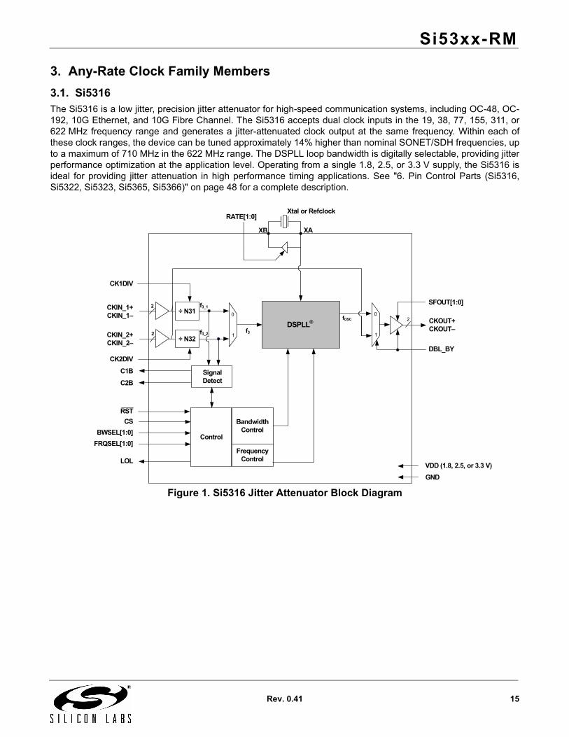
3.1. Si5316The Si5316 is a low jitter, precision jitter attenuator for high-speed communication systems, including OC-48, OC-192, 10G Ethernet, and 10G Fibre Channel. The Si5316 accepts dual clock inputs in the 19, 38, 77, 155, 311, or622 MHz frequency range and generates a jitter-attenuated clock output at the same frequency. Within each ofthese clock ranges, the device can be tuned approximately 14% higher than nominal SONET/SDH frequencies, upto a maximum of 710 MHz in the 622 MHz range. The DSPLL loop bandwidth is digitally selectable, providing jitterperformance optimization at the application level. Operating from a single 1.8, 2.5, or 3.3 V supply, the Si5316 isideal for providing jitter attenuation in high performance timing applications. See "6. Pin Control Parts (Si5316,Si5322, Si5323, Si5365, Si5366)" on page 48 for a complete description.
Figure 1. Si5316 Jitter Attenuator Block Diagram
2
DSPLL®
C1B
CS
LOL
BWSEL[1:0]
DBL_BY
Xtal or Refclock
SFOUT[1:0]
CKOUT+CKOUT–
CKIN_1+CKIN_1–
CKIN_2+CKIN_2–
Control
Signal Detect
VDD (1.8, 2.5, or 3.3 V)
GND
Frequency Control
Bandwidth Control
C2B
2
FRQSEL[1:0]
RST
0
1
RATE[1:0]
XAXB
fOSC 20
1
÷ N31
÷ N32
f3_1
f3_2
CK1DIV
CK2DIV
f3
Si53xx-RM
16 Rev. 0.41
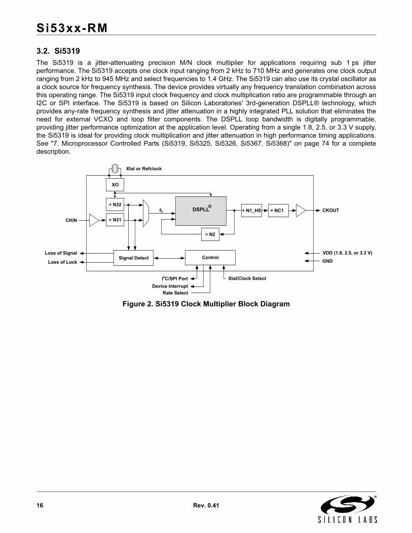
3.2. Si5319The Si5319 is a jitter-attenuating precision M/N clock multiplier for applications requiring sub 1 ps jitterperformance. The Si5319 accepts one clock input ranging from 2 kHz to 710 MHz and generates one clock outputranging from 2 kHz to 945 MHz and select frequencies to 1.4 GHz. The Si5319 can also use its crystal oscillator asa clock source for frequency synthesis. The device provides virtually any frequency translation combination acrossthis operating range. The Si5319 input clock frequency and clock multiplication ratio are programmable through anI2C or SPI interface. The Si5319 is based on Silicon Laboratories' 3rd-generation DSPLL® technology, whichprovides any-rate frequency synthesis and jitter attenuation in a highly integrated PLL solution that eliminates theneed for external VCXO and loop filter components. The DSPLL loop bandwidth is digitally programmable,providing jitter performance optimization at the application level. Operating from a single 1.8, 2.5, or 3.3 V supply,the Si5319 is ideal for providing clock multiplication and jitter attenuation in high performance timing applications.See "7. Microprocessor Controlled Parts (Si5319, Si5325, Si5326, Si5367, Si5368)" on page 74 for a completedescription.
Figure 2. Si5319 Clock Multiplier Block Diagram
DSPLL®
Loss of Signal
Xtal or Refclock
CKIN
CKOUT
÷ N31
÷ N2
Signal Detect
Device Interrupt
VDD (1.8, 2.5, or 3.3 V)
GNDLoss of Lock
Xtal/Clock SelectI2C/SPI Port
Control
Rate Select
÷ N32
XO
f3 ÷ N1_HS ÷ NC1
Si53xx-RM
Rev. 0.41 17
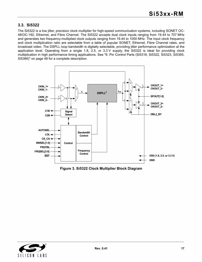
3.3. Si5322The Si5322 is a low jitter, precision clock multiplier for high-speed communication systems, including SONET OC-48/OC-192, Ethernet, and Fibre Channel. The Si5322 accepts dual clock inputs ranging from 19.44 to 707 MHzand generates two frequency-multiplied clock outputs ranging from 19.44 to 1050 MHz. The input clock frequencyand clock multiplication ratio are selectable from a table of popular SONET, Ethernet, Fibre Channel rates, andbroadcast video. The DSPLL loop bandwidth is digitally selectable, providing jitter performance optimization at theapplication level. Operating from a single 1.8, 2.5, or 3.3 V supply, the Si5322 is ideal for providing clockmultiplication in high performance timing applications. See "6. Pin Control Parts (Si5316, Si5322, Si5323, Si5365,Si5366)" on page 48 for a complete description.
Figure 3. Si5322 Clock Multiplier Block Diagram
DSPLL®
C1B
LOL
CS_CA
BWSEL[1:0]
DBL2_BY
SFOUT[1:0]
CKOUT_2+CKOUT_2–
CKIN_1+CKIN_1–
CKOUT_1+CKOUT_2–
CKIN_2+CKIN_2–
Control
AUTOSEL
FRQTBL
Signal Detect
VDD (1.8, 2.5, or 3.3 V)
GND
Frequency Control
Bandwidth Control
C2B
2
2
FRQSEL[3:0]
RST
0
1
fOSC
2
2
0
1
0
1f3
Si53xx-RM
18 Rev. 0.41
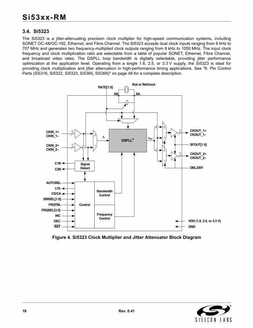
3.4. Si5323The Si5323 is a jitter-attenuating precision clock multiplier for high-speed communication systems, includingSONET OC-48/OC-192, Ethernet, and Fibre Channel. The Si5323 accepts dual clock inputs ranging from 8 kHz to707 MHz and generates two frequency-multiplied clock outputs ranging from 8 kHz to 1050 MHz. The input clockfrequency and clock multiplication ratio are selectable from a table of popular SONET, Ethernet, Fibre Channel,and broadcast video rates. The DSPLL loop bandwidth is digitally selectable, providing jitter performanceoptimization at the application level. Operating from a single 1.8, 2.5, or 3.3 V supply, the Si5323 is ideal forproviding clock multiplication and jitter attenuation in high-performance timing applications. See "6. Pin ControlParts (Si5316, Si5322, Si5323, Si5365, Si5366)" on page 48 for a complete description.
Figure 4. Si5323 Clock Multiplier and Jitter Attenuator Block Diagram
DSPLL®
C1B
LOL
CS/CA
BWSEL[1:0]
DBL2/BY
Xtal or Refclock
SFOUT[1:0]
CKOUT_2+CKOUT_2–
CKIN_1+CKIN_1–
CKOUT_1+CKOUT_1–
CKIN_2+CKIN_2–
Control
AUTOSEL
FRQTBL
Signal Detect
VDD (1.8, 2.5, or 3.3 V)
GND
Frequency Control
Bandwidth Control
C2B
2
2
FRQSEL[3:0]
INC
DEC
RST
0
1
RATE[1:0]
XAXB
fOSC
2
2
0
1
0
1f3
Si53xx-RM
Rev. 0.41 19
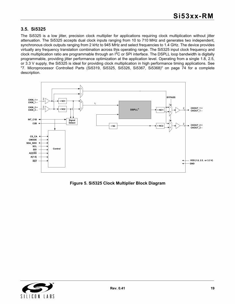
3.5. Si5325The Si5325 is a low jitter, precision clock multiplier for applications requiring clock multiplication without jitterattenuation. The Si5325 accepts dual clock inputs ranging from 10 to 710 MHz and generates two independent,synchronous clock outputs ranging from 2 kHz to 945 MHz and select frequencies to 1.4 GHz. The device providesvirtually any frequency translation combination across this operating range. The Si5325 input clock frequency andclock multiplication ratio are programmable through an I2C or SPI interface. The DSPLL loop bandwidth is digitallyprogrammable, providing jitter performance optimization at the application level. Operating from a single 1.8, 2.5,or 3.3 V supply, the Si5325 is ideal for providing clock multiplication in high performance timing applications. See"7. Microprocessor Controlled Parts (Si5319, Si5325, Si5326, Si5367, Si5368)" on page 74 for a completedescription.
Figure 5. Si5325 Clock Multiplier Block Diagram
÷ N31
INT_C1B
÷ NC1
÷ NC2
Signal Detect
VDD (1.8, 2.5, or 3.3 V)
GND
C2B
0
1
CKOUT_2 +CKOUT_2 –
CKOUT_1 +CKOUT_1 –
/
/2
2
1
0
1
0
CS_CA
SDA_SDO
RST
SCLControlSDI
A[2]/SS
A[1:0]
CMODE
CKIN_1 +CKIN_1 –
2
2CKIN_2 +CKIN_2 – ÷ N32
0
1
BYPASS
÷ N2
f3
DSPLL®
Si53xx-RM
20 Rev. 0.41
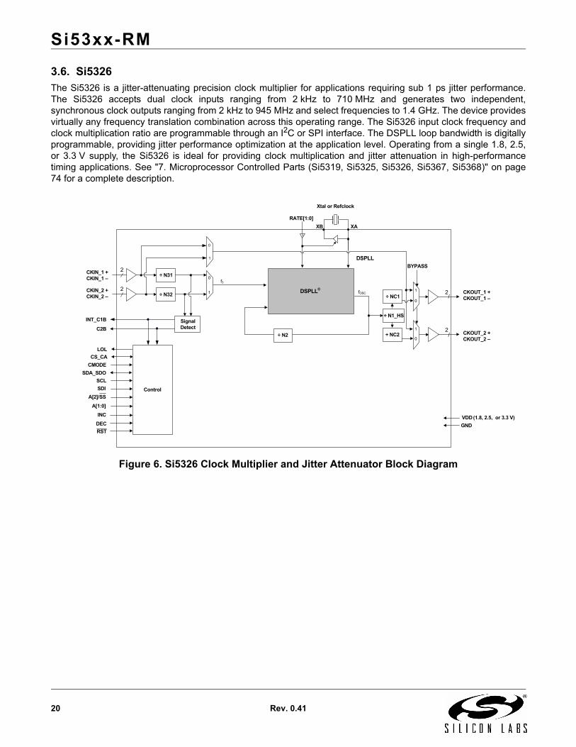
3.6. Si5326The Si5326 is a jitter-attenuating precision clock multiplier for applications requiring sub 1 ps jitter performance.The Si5326 accepts dual clock inputs ranging from 2 kHz to 710 MHz and generates two independent,synchronous clock outputs ranging from 2 kHz to 945 MHz and select frequencies to 1.4 GHz. The device providesvirtually any frequency translation combination across this operating range. The Si5326 input clock frequency andclock multiplication ratio are programmable through an I2C or SPI interface. The DSPLL loop bandwidth is digitallyprogrammable, providing jitter performance optimization at the application level. Operating from a single 1.8, 2.5,or 3.3 V supply, the Si5326 is ideal for providing clock multiplication and jitter attenuation in high-performancetiming applications. See "7. Microprocessor Controlled Parts (Si5319, Si5325, Si5326, Si5367, Si5368)" on page74 for a complete description.
Figure 6. Si5326 Clock Multiplier and Jitter Attenuator Block Diagram
÷ N31
INT_C1B
Xtal or Refclock
÷ NC1
÷ NC2
Signal Detect
VDD (1.8, 2.5, or 3.3 V)
GND
C2B
0
1
f3
CKOUT_2 +CKOUT_2 –
CKOUT_1 +CKOUT_1 –
/
/2
2
1
0
1
0
fOSC
RATE[1:0]
LOL
CS_CA
SDA_SDO
INC
DEC
RST
SCL
ControlSDI
A[2]/SS
A[1:0]
XAXB
CMODE
CKIN_1 +CKIN_1 –
2
2CKIN_2 +CKIN_2 – ÷ N32
0
1
3
BYPASS
÷ N2
DSPLL
÷ N1_HS
DSPLL®
Si53xx-RM
Rev. 0.41 21
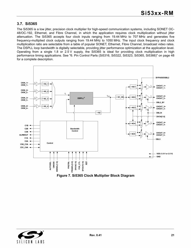
3.7. Si5365The Si5365 is a low jitter, precision clock multiplier for high-speed communication systems, including SONET OC-48/OC-192, Ethernet, and Fibre Channel, in which the application requires clock multiplication without jitterattenuation. The Si5365 accepts four clock inputs ranging from 19.44 MHz to 707 MHz and generates fivefrequency-multiplied clock outputs ranging from 19.44 MHz to 1050 MHz. The input clock frequency and clockmultiplication ratio are selectable from a table of popular SONET, Ethernet, Fibre Channel, broadcast video rates.The DSPLL loop bandwidth is digitally selectable, providing jitter performance optimization at the application level.Operating from a single 1.8 or 2.5 V supply, the Si5365 is ideal for providing clock multiplication in highperformance timing applications. See "6. Pin Control Parts (Si5316, Si5322, Si5323, Si5365, Si5366)" on page 48for a complete description.
Figure 7. Si5365 Clock Multiplier Block Diagram
C2A
CS0_C3A
C2B
CS1_C4A
ALRMOUT
C1A
CKIN_1+CKIN_1–
CKIN_2+CKIN_2–
C3B
CKIN_3+CKIN_3–
CKIN_4+CKIN_4–
C1B
VDD (1.8 V or 2.5 V)
GND
CKOUT_1+CKOUT_1–
÷ NC11
0
CKOUT_2+CKOUT_2–
÷ NC21
0
CKOUT_3+CKOUT_3–
÷ NC31
0
CKOUT_4+CKOUT_4–
÷ NC41
0
2
2
2
2
2
2
2
2
fOSC
f3
DBL2_BY
DBL34
DBL5
BW
SE
L[1
:0]
FR
QS
EL
[3:0
]
DIV
34[1
:0]
FO
S_C
TL
SF
OU
T[1
:0]
RS
T
CM
OD
E
AU
TO
SE
L
BYPASS/DSBL2
Control
÷ N3_2
÷ N3_1
Bandwidth Control
÷ N2
÷ N3_3
÷ N3_4
CKOUT_5+CKOUT_5–
÷ NC51
0
2
FR
QT
BL
DIV34[1:0]
÷ N1_HSDSPLL®
Si53xx-RM
22 Rev. 0.41
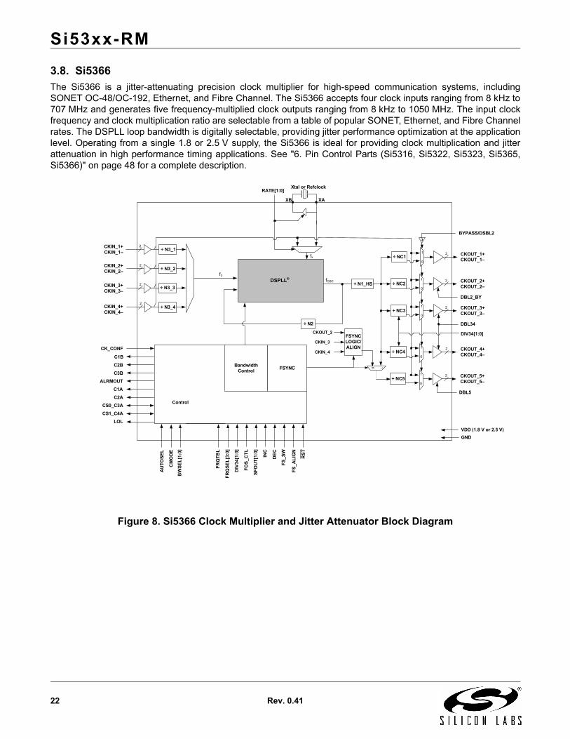
3.8. Si5366The Si5366 is a jitter-attenuating precision clock multiplier for high-speed communication systems, includingSONET OC-48/OC-192, Ethernet, and Fibre Channel. The Si5366 accepts four clock inputs ranging from 8 kHz to707 MHz and generates five frequency-multiplied clock outputs ranging from 8 kHz to 1050 MHz. The input clockfrequency and clock multiplication ratio are selectable from a table of popular SONET, Ethernet, and Fibre Channelrates. The DSPLL loop bandwidth is digitally selectable, providing jitter performance optimization at the applicationlevel. Operating from a single 1.8 or 2.5 V supply, the Si5366 is ideal for providing clock multiplication and jitterattenuation in high performance timing applications. See "6. Pin Control Parts (Si5316, Si5322, Si5323, Si5365,Si5366)" on page 48 for a complete description.
Figure 8. Si5366 Clock Multiplier and Jitter Attenuator Block Diagram
C2A
CS0_C3A
C2B
CS1_C4A
ALRMOUT
C1A
CKIN_1+CKIN_1–
CKIN_2+CKIN_2–
C3B
CKIN_3+CKIN_3–
CKIN_4+CKIN_4–
C1B
CKIN_3
CKIN_4
CKOUT_2
VDD (1.8 V or 2.5 V)
GND
CKOUT_1+CKOUT_1–
÷ NC11
0
CKOUT_2+CKOUT_2–
÷ NC21
0
CKOUT_3+CKOUT_3–
÷ NC31
0
CKOUT_4+CKOUT_4–
÷ NC41
0
2
2
2
2
2
2
2
2
fOSC
Xtal or RefclockRATE[1:0]
XAXB
fx
f3
DBL2_BY
DBL34
DBL5
FSYNCLOGIC/ALIGNCK_CONF
BW
SE
L[1
:0]
FR
QS
EL
[3:0
]
DIV
34[1
:0]
FO
S_
CT
L
SF
OU
T[1
:0]
INC
DE
C
FS
_S
W
FS
_AL
IGN
RS
T
CM
OD
E
AU
TO
SE
L
BYPASS/DSBL2
LOL
Control
÷ N3_2
÷ N3_1
Bandwidth Control
FSYNC
÷ N2
3
÷ N3_3
÷ N3_4
CKOUT_5+CKOUT_5–
÷ NC51
0
2
10
FR
QT
BL
DIV34[1:0]
÷ N1_HSDSPLL®
Si53xx-RM
Rev. 0.41 23
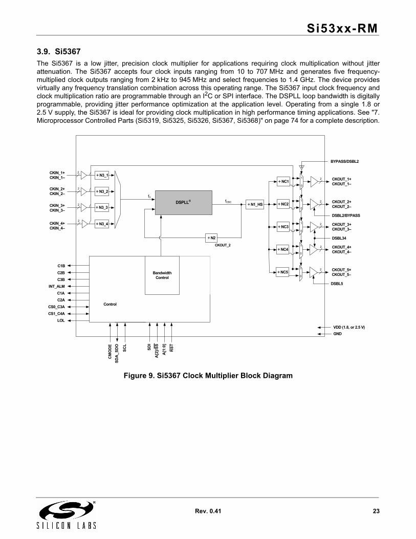
3.9. Si5367The Si5367 is a low jitter, precision clock multiplier for applications requiring clock multiplication without jitterattenuation. The Si5367 accepts four clock inputs ranging from 10 to 707 MHz and generates five frequency-multiplied clock outputs ranging from 2 kHz to 945 MHz and select frequencies to 1.4 GHz. The device providesvirtually any frequency translation combination across this operating range. The Si5367 input clock frequency andclock multiplication ratio are programmable through an I2C or SPI interface. The DSPLL loop bandwidth is digitallyprogrammable, providing jitter performance optimization at the application level. Operating from a single 1.8 or2.5 V supply, the Si5367 is ideal for providing clock multiplication in high performance timing applications. See "7.Microprocessor Controlled Parts (Si5319, Si5325, Si5326, Si5367, Si5368)" on page 74 for a complete description.
Figure 9. Si5367 Clock Multiplier Block Diagram
C2A
CS0_C3A
C2B
CS1_C4A
INT_ALM
C1A
CKIN_1+CKIN_1–
CKIN_2+CKIN_2–
C3B
CKIN_3+CKIN_3–
CKIN_4+CKIN_4–
C1B
CKOUT_2
VDD (1.8, or 2.5 V)
GND
CKOUT_1+CKOUT_1–
÷ NC11
0
CKOUT_2+CKOUT_2–
÷ NC21
0
CKOUT_3+CKOUT_3–
÷ NC31
0
CKOUT_4+CKOUT_4–
÷ NC41
0
2
2
2
2
2
2
2
2
fOSC
f3
DSBL2/BYPASS
DSBL34
DSBL5
SD
A_
SD
O
SC
L
SD
I
A[1
:0]
RS
T
CM
OD
E
BYPASS/DSBL2
LOL
Control
÷ N3_2
÷ N3_1
Bandwidth Control
÷ N2
3
÷ N3_3
÷ N3_4
CKOUT_5+CKOUT_5–
÷ NC51
0
2
A[2
]/S
S
÷ N1_HSDSPLL®
Si53xx-RM
24 Rev. 0.41
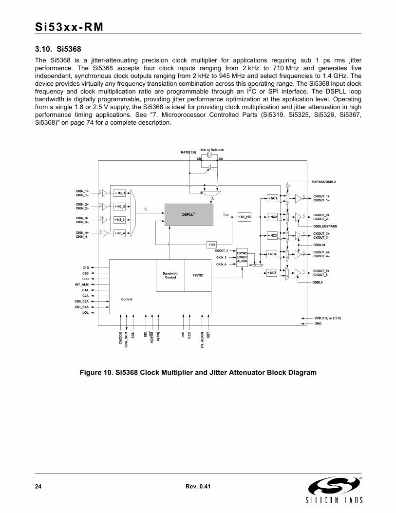
3.10. Si5368The Si5368 is a jitter-attenuating precision clock multiplier for applications requiring sub 1 ps rms jitterperformance. The Si5368 accepts four clock inputs ranging from 2 kHz to 710 MHz and generates fiveindependent, synchronous clock outputs ranging from 2 kHz to 945 MHz and select frequencies to 1.4 GHz. Thedevice provides virtually any frequency translation combination across this operating range. The Si5368 input clockfrequency and clock multiplication ratio are programmable through an I2C or SPI interface. The DSPLL loopbandwidth is digitally programmable, providing jitter performance optimization at the application level. Operatingfrom a single 1.8 or 2.5 V supply, the Si5368 is ideal for providing clock multiplication and jitter attenuation in highperformance timing applications. See "7. Microprocessor Controlled Parts (Si5319, Si5325, Si5326, Si5367,Si5368)" on page 74 for a complete description.
Figure 10. Si5368 Clock Multiplier and Jitter Attenuator Block Diagram
C2A
CS0_C3A
C2B
CS1_C4A
INT_ALM
C1A
CKIN_1+CKIN_1–
CKIN_2+CKIN_2–
C3B
CKIN_3+CKIN_3–
CKIN_4+CKIN_4–
C1B
CKIN_3
CKIN_4
CKOUT_2
VDD (1.8, or 2.5 V)
GND
CKOUT_1+CKOUT_1–
÷ NC11
0
CKOUT_2+CKOUT_2–
÷ NC21
0
CKOUT_3+CKOUT_3–
÷ NC31
0
CKOUT_4+CKOUT_4–
÷ NC41
0
2
2
2
2
2
2
2
2
fOSC
Xtal or RefclockRATE[1:0]
XAXB
fx
DSBL2/BYPASS
DSBL34
DSBL5
FSYNCLOGIC/ALIGN
SD
A_
SD
O
SC
L
SD
I
A[1
:0]
INC
DE
C
FS
_AL
IGN
RS
T
CM
OD
E
BYPASS/DSBL2
LOL
Control
÷ N3_2
÷ N3_1
Bandwidth Control
FSYNC
÷ N2
3
÷ N3_3
÷ N3_4
CKOUT_5+CKOUT_5–
÷ NC51
0
2
10
A[2
]/S
S
÷ N1_HSDSPLL®
f3
Si53xx-RM
Rev. 0.41 25
4. Specifications
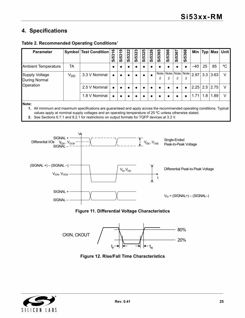
Figure 11. Differential Voltage Characteristics
Figure 12. Rise/Fall Time Characteristics
Table 2. Recommended Operating Conditions1
Parameter Symbol Test Condition
Si5
31
6
Si5
31
9
Si5
32
2
Si5
32
3
Si5
32
5
Si5
32
6
Si5
36
5
Si5
36
6
Si5
36
7
Si5
36
8 Min Typ Max Unit
Ambient Temperature TA –40 25 85 ºC
Supply Voltage During Normal Operation
VDD 3.3 V Nominal Note
2
Note
2
Note
2
Note
22.97 3.3 3.63 V
2.5 V Nominal 2.25 2.5 2.75 V
1.8 V Nominal 1.71 1.8 1.89 V
Note:1. All minimum and maximum specifications are guaranteed and apply across the recommended operating conditions. Typical
values apply at nominal supply voltages and an operating temperature of 25 ºC unless otherwise stated. 2. See Sections 6.7.1 and 8.2.1 for restrictions on output formats for TQFP devices at 3.3 V.
VISE, VOSE
VID,VOD
Differential I/Os
VICM, VOCM
Single-EndedPeak-to-Peak Voltage
Differential Peak-to-Peak Voltage
SIGNAL +
SIGNAL –
(SIGNAL +) – (SIGNAL –)
V
t
SIGNAL +
SIGNAL –VID = (SIGNAL+) – (SIGNAL–)
VICM , VOCM
tF tR
80%
20%CKIN, CKOUT
Si53xx-RM
26 Rev. 0.41
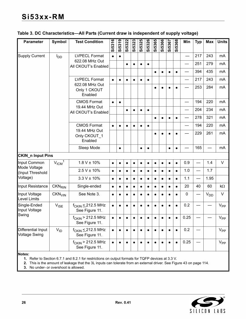
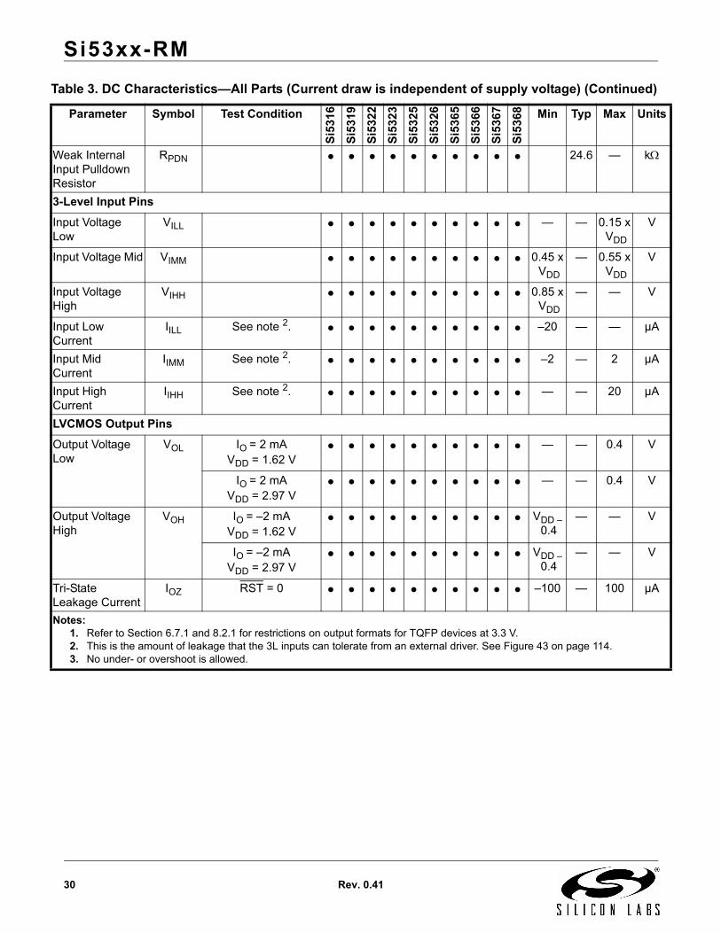
Table 3. DC Characteristics—All Parts (Current draw is independent of supply voltage)
Parameter Symbol Test Condition
Si5
316
Si5
319
Si5
322
Si5
323
Si5
325
Si5
326
Si5
365
Si5
366
Si5
367
Si5
368 Min Typ Max Units
Supply Current IDD LVPECL Format622.08 MHz Out
All CKOUT’s Enabled
— 217 243 mA
— 251 279 mA
— 394 435 mA
LVPECL Format622.08 MHz OutOnly 1 CKOUT
Enabled
— 217 243 mA
— 253 284 mA
CMOS Format19.44 MHz Out
All CKOUT’s Enabled
— 194 220 mA
— 204 234 mA
— 278 321 mA
CMOS Format19.44 MHz OutOnly CKOUT_1
Enabled
— 194 220 mA
— 229 261 mA
Sleep Mode — 165 — mA
CKIN_n Input Pins
Input Common Mode Voltage(Input Threshold Voltage)
VICM1 1.8 V ± 10% 0.9 — 1.4 V
2.5 V ± 10% 1.0 — 1.7
3.3 V ± 10% 1.1 — 1.95
Input Resistance CKNRIN Single-ended 20 40 60 k
Input Voltage Level Limits
CKNVIN See Note 3. 0 — VDD V
Single-Ended Input Voltage Swing
VISE fCKIN < 212.5 MHzSee Figure 11.
0.2 — — VPP
fCKIN > 212.5 MHzSee Figure 11.
0.25 — — VPP
Differential Input Voltage Swing
VID fCKIN < 212.5 MHzSee Figure 11.
0.2 — VPP
fCKIN > 212.5 MHzSee Figure 11.
0.25 — VPP
Notes:1. Refer to Section 6.7.1 and 8.2.1 for restrictions on output formats for TQFP devices at 3.3 V.2. This is the amount of leakage that the 3L inputs can tolerate from an external driver. See Figure 43 on page 114.3. No under- or overshoot is allowed.
Si53xx-RM
Rev. 0.41 27
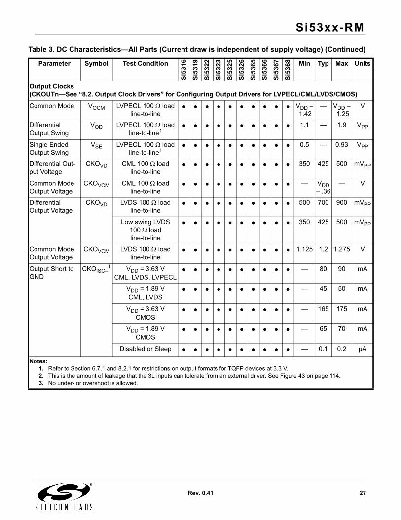
Output Clocks (CKOUTn—See “8.2. Output Clock Drivers” for Configuring Output Drivers for LVPECL/CML/LVDS/CMOS)
Common Mode VOCM LVPECL 100 load line-to-line
VDD –1.42
— VDD –1.25
V
Differential Output Swing
VOD LVPECL 100 load line-to-line1
1.1 — 1.9 VPP
Single Ended Output Swing
VSE LVPECL 100 load line-to-line1
0.5 — 0.93 VPP
Differential Out-put Voltage
CKOVD CML 100 load line-to-line
350 425 500 mVPP
Common Mode Output Voltage
CKOVCM CML 100 load line-to-line
— VDD – .36
— V
Differential Output Voltage
CKOVD LVDS 100 load line-to-line
500 700 900 mVPP
Low swing LVDS 100 load line-to-line
350 425 500 mVPP
Common Mode Output Voltage
CKOVCM LVDS 100 load line-to-line
1.125 1.2 1.275 V
Output Short to GND
CKOISC–1 VDD = 3.63 V
CML, LVDS, LVPECL — 80 90 mA
VDD = 1.89 VCML, LVDS
— 45 50 mA
VDD = 3.63 VCMOS
— 165 175 mA
VDD = 1.89 VCMOS
— 65 70 mA
Disabled or Sleep — 0.1 0.2 µA
Table 3. DC Characteristics—All Parts (Current draw is independent of supply voltage) (Continued)
Parameter Symbol Test Condition
Si5
31
6
Si5
31
9
Si5
32
2
Si5
32
3
Si5
32
5
Si5
32
6
Si5
36
5
Si5
36
6
Si5
36
7
Si5
36
8 Min Typ Max Units
Notes:1. Refer to Section 6.7.1 and 8.2.1 for restrictions on output formats for TQFP devices at 3.3 V.2. This is the amount of leakage that the 3L inputs can tolerate from an external driver. See Figure 43 on page 114.3. No under- or overshoot is allowed.
Si53xx-RM
28 Rev. 0.41
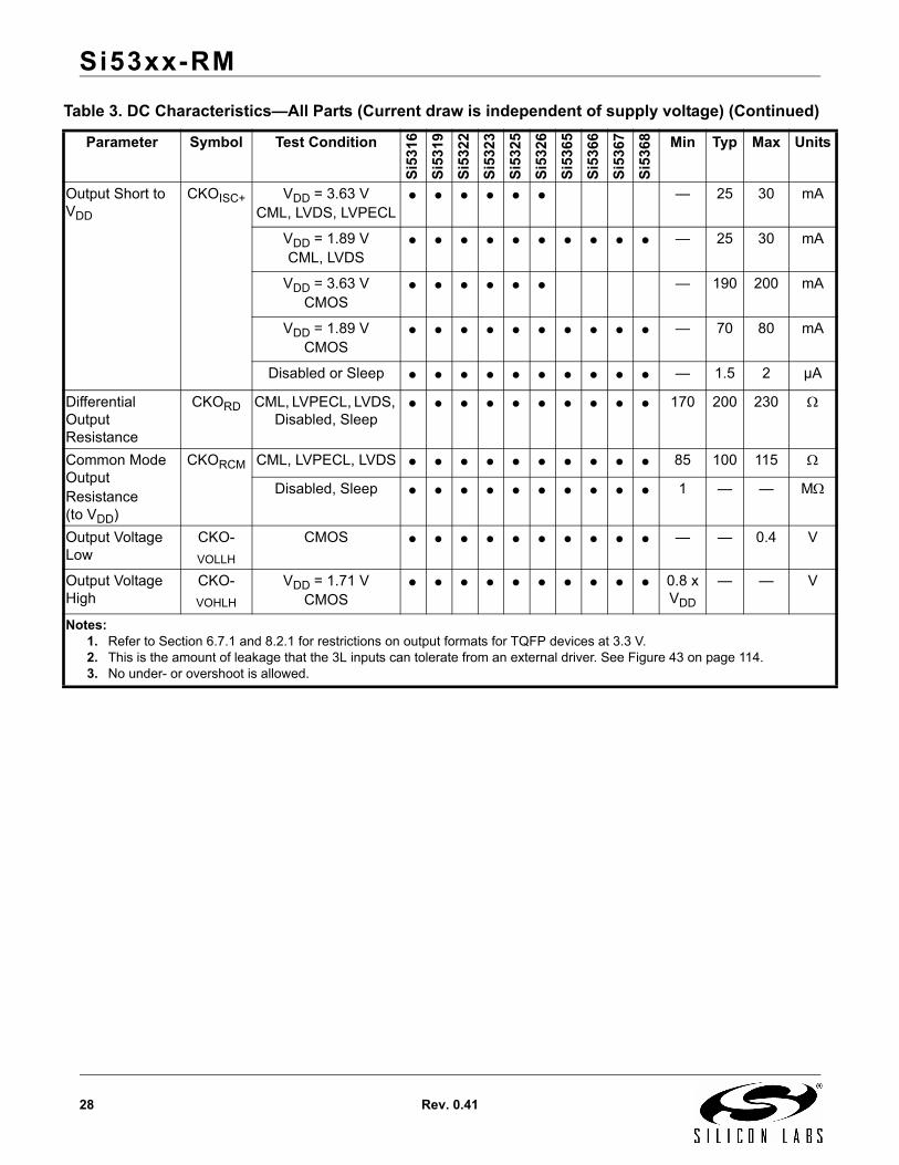
Output Short to VDD
CKOISC+ VDD = 3.63 VCML, LVDS, LVPECL
— 25 30 mA
VDD = 1.89 VCML, LVDS
— 25 30 mA
VDD = 3.63 VCMOS
— 190 200 mA
VDD = 1.89 VCMOS
— 70 80 mA
Disabled or Sleep — 1.5 2 µA
Differential Output Resistance
CKORD CML, LVPECL, LVDS, Disabled, Sleep
170 200 230
Common Mode OutputResistance (to VDD)
CKORCM CML, LVPECL, LVDS 85 100 115
Disabled, Sleep 1 — — M
Output Voltage Low
CKO-
VOLLH
CMOS — — 0.4 V
Output Voltage High
CKO-
VOHLH
VDD = 1.71 VCMOS
0.8 xVDD
— — V
Table 3. DC Characteristics—All Parts (Current draw is independent of supply voltage) (Continued)
Parameter Symbol Test Condition
Si5
31
6
Si5
31
9
Si5
32
2
Si5
32
3
Si5
32
5
Si5
32
6
Si5
36
5
Si5
36
6
Si5
36
7
Si5
36
8 Min Typ Max Units
Notes:1. Refer to Section 6.7.1 and 8.2.1 for restrictions on output formats for TQFP devices at 3.3 V.2. This is the amount of leakage that the 3L inputs can tolerate from an external driver. See Figure 43 on page 114.3. No under- or overshoot is allowed.
Si53xx-RM
Rev. 0.41 29
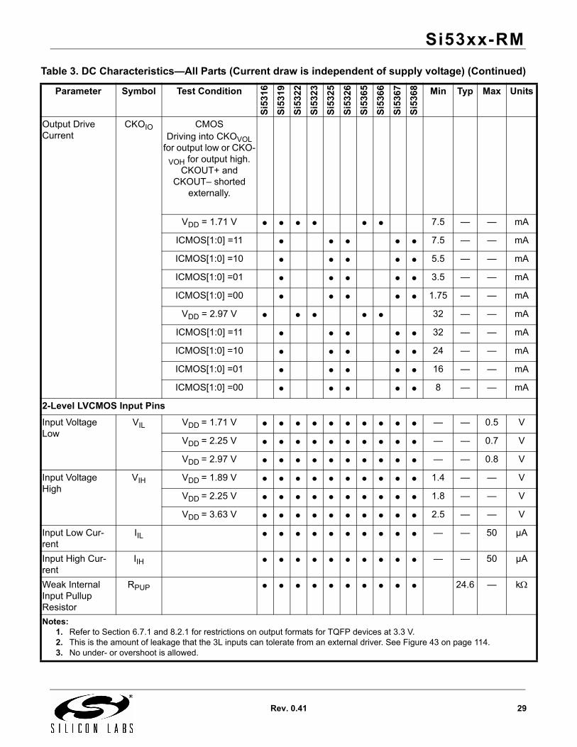
Output Drive Current
CKOIO CMOSDriving into CKOVOL
for output low or CKO-
VOH for output high. CKOUT+ and
CKOUT– shorted externally.
VDD = 1.71 V 7.5 — — mA
ICMOS[1:0] =11 7.5 — — mA
ICMOS[1:0] =10 5.5 — — mA
ICMOS[1:0] =01 3.5 — — mA
ICMOS[1:0] =00 1.75 — — mA
VDD = 2.97 V 32 — — mA
ICMOS[1:0] =11 32 — — mA
ICMOS[1:0] =10 24 — — mA
ICMOS[1:0] =01 16 — — mA
ICMOS[1:0] =00 8 — — mA
2-Level LVCMOS Input Pins
Input Voltage Low
VIL VDD = 1.71 V — — 0.5 V
VDD = 2.25 V — — 0.7 V
VDD = 2.97 V — — 0.8 V
Input Voltage High
VIH VDD = 1.89 V 1.4 — — V
VDD = 2.25 V 1.8 — — V
VDD = 3.63 V 2.5 — — V
Input Low Cur-rent
IIL — — 50 µA
Input High Cur-rent
IIH — — 50 µA
Weak Internal Input Pullup Resistor
RPUP 24.6 — k
Table 3. DC Characteristics—All Parts (Current draw is independent of supply voltage) (Continued)
Parameter Symbol Test Condition
Si5
31
6
Si5
31
9
Si5
32
2
Si5
32
3
Si5
32
5
Si5
32
6
Si5
36
5
Si5
36
6
Si5
36
7
Si5
36
8 Min Typ Max Units
Notes:1. Refer to Section 6.7.1 and 8.2.1 for restrictions on output formats for TQFP devices at 3.3 V.2. This is the amount of leakage that the 3L inputs can tolerate from an external driver. See Figure 43 on page 114.3. No under- or overshoot is allowed.
Si53xx-RM
30 Rev. 0.41
Weak Internal Input Pulldown Resistor
RPDN 24.6 — k
3-Level Input Pins
Input Voltage Low
VILL — — 0.15 xVDD
V
Input Voltage Mid VIMM 0.45 xVDD
— 0.55 xVDD
V
Input Voltage High
VIHH 0.85 xVDD
— — V
Input Low Current
IILL See note 2. –20 — — µA
Input Mid Current
IIMM See note 2. –2 — 2 µA
Input High Current
IIHH See note 2. — — 20 µA
LVCMOS Output Pins
Output Voltage Low
VOL IO = 2 mAVDD = 1.62 V
— — 0.4 V
IO = 2 mAVDD = 2.97 V
— — 0.4 V
Output Voltage High
VOH IO = –2 mAVDD = 1.62 V
VDD –0.4
— — V
IO = –2 mAVDD = 2.97 V
VDD –0.4
— — V
Tri-State Leakage Current
IOZ RST = 0 –100 — 100 µA
Table 3. DC Characteristics—All Parts (Current draw is independent of supply voltage) (Continued)
Parameter Symbol Test Condition
Si5
31
6
Si5
31
9
Si5
32
2
Si5
32
3
Si5
32
5
Si5
32
6
Si5
36
5
Si5
36
6
Si5
36
7
Si5
36
8 Min Typ Max Units
Notes:1. Refer to Section 6.7.1 and 8.2.1 for restrictions on output formats for TQFP devices at 3.3 V.2. This is the amount of leakage that the 3L inputs can tolerate from an external driver. See Figure 43 on page 114.3. No under- or overshoot is allowed.
Si53xx-RM
Rev. 0.41 31
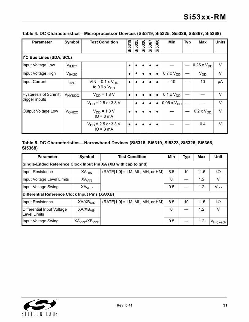
Table 4. DC Characteristics—Microprocessor Devices (Si5319, Si5325, Si5326, Si5367, Si5368)
Parameter Symbol Test Condition
Si5
319
Si5
325
Si5
326
Si5
367
Si5
368 Min Typ Max Units
I2C Bus Lines (SDA, SCL)
Input Voltage Low VILI2C — — 0.25 x VDD V
Input Voltage High VIHI2C 0.7 x VDD — VDD V
Input Current III2C VIN = 0.1 x VDDto 0.9 x VDD
–10 — 10 µA
Hysteresis of Schmitt trigger inputs
VHYSI2C VDD = 1.8 V 0.1 x VDD — — V
VDD = 2.5 or 3.3 V 0.05 x VDD — — V
Output Voltage Low VOHI2C VDD = 1.8 VIO = 3 mA
— — 0.2 x VDD V
VDD = 2.5 or 3.3 VIO = 3 mA
— — 0.4 V
Table 5. DC Characteristics—Narrowband Devices (Si5316, Si5319, Si5323, Si5326, Si5366, Si5368)
Parameter Symbol Test Condition Min Typ Max Unit
Single-Ended Reference Clock Input Pin XA (XB with cap to gnd)
Input Resistance XARIN (RATE[1:0] = LM, ML, MH, or HM) 8.5 10 11.5 k
Input Voltage Level Limits XAVIN 0 — 1.2 V
Input Voltage Swing XAVPP 0.5 — 1.2 VPP
Differential Reference Clock Input Pins (XA/XB)
Input Resistance XA/XBRIN (RATE[1:0] = LM, ML, MH, or HM) 8.5 10 11.5 k
Differential Input Voltage Level Limits
XA/XBVIN 0 — 1.2 V
Input Voltage Swing XAVPP/XBVPP 0.5 — 1.2 VPP, each
Si53xx-RM
32 Rev. 0.41
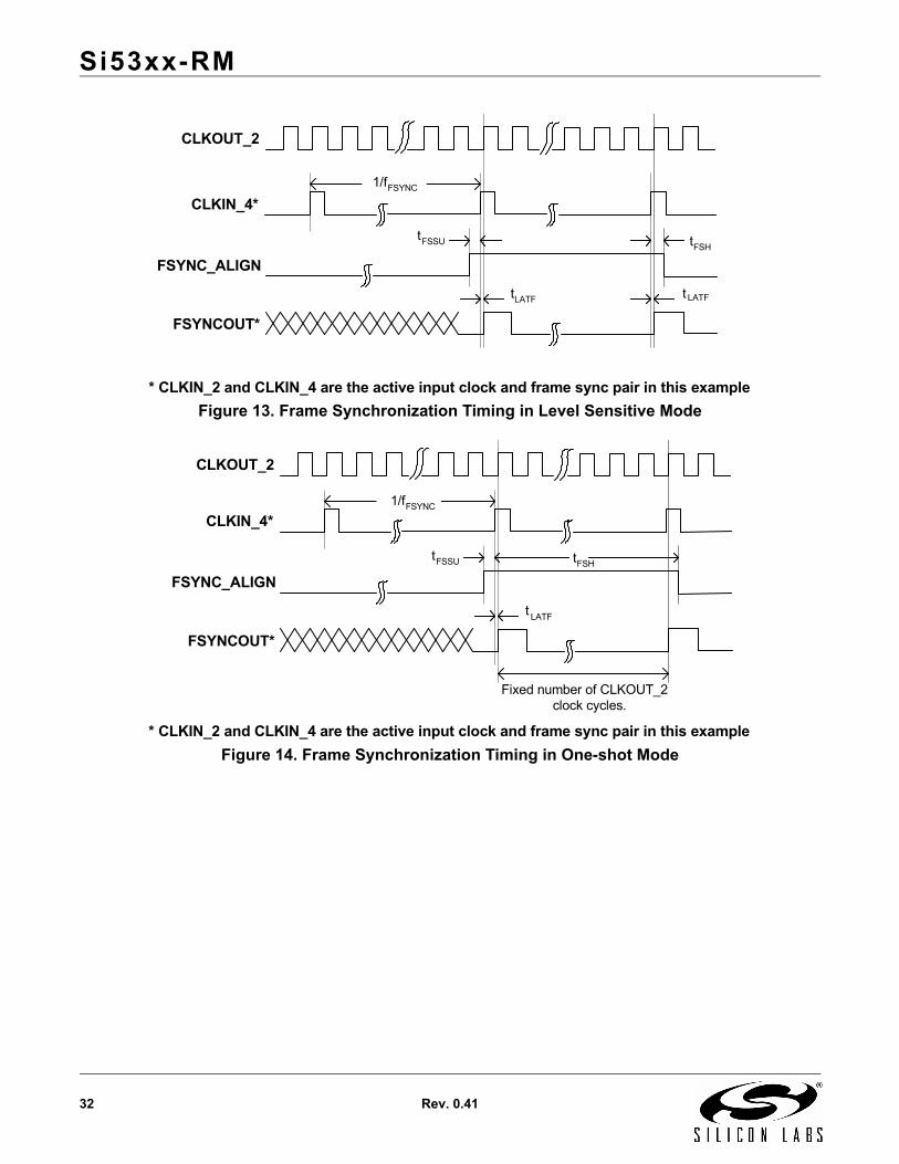
Figure 13. Frame Synchronization Timing in Level Sensitive Mode
Figure 14. Frame Synchronization Timing in One-shot Mode
CLKOUT_2
CLKIN_4*
FSYNC_ALIGN
FSYNCOUT*
* CLKIN_2 and CLKIN_4 are the active input clock and frame sync pair in this example
tFSSU tFSH
tLATF t
1/fFSYNC
LATF
CLKOUT_2
CLKIN_4*
FSYNC_ALIGN
FSYNCOUT*
* CLKIN_2 and CLKIN_4 are the active input clock and frame sync pair in this example
tFSSU tFSH
t
1/fFSYNC
Fixed number of CLKOUT_2clock cycles.
LATF
Si53xx-RM
Rev. 0.41 33
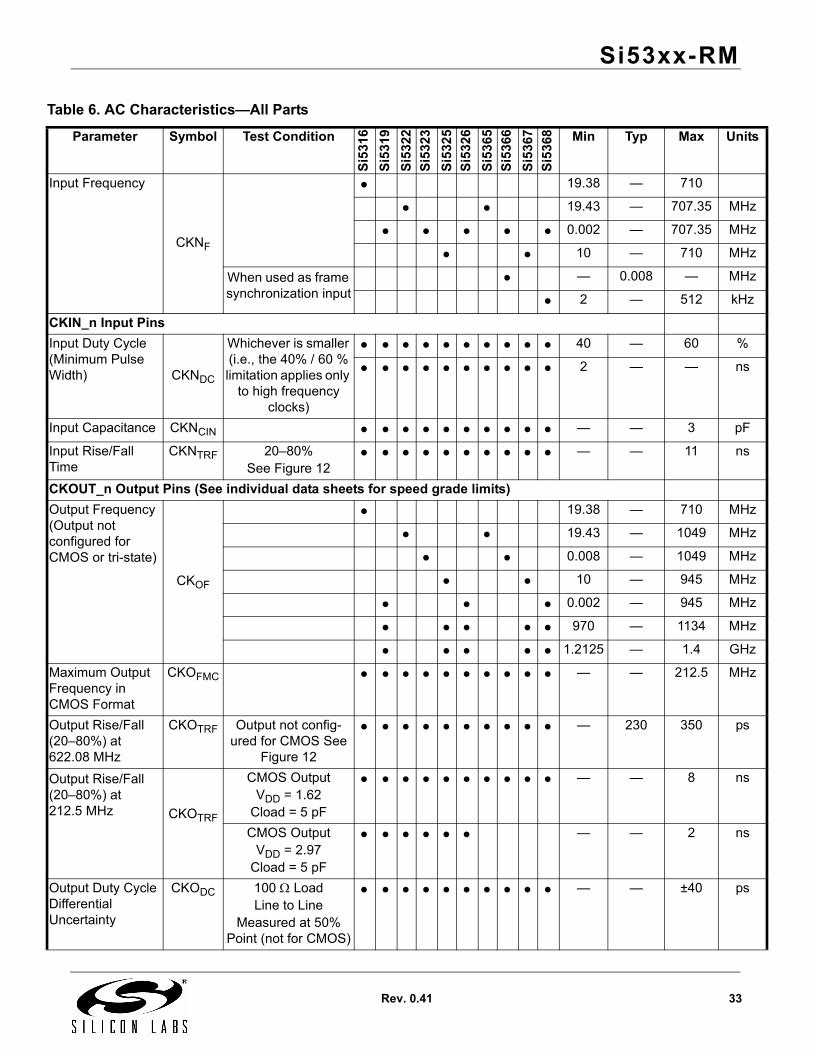
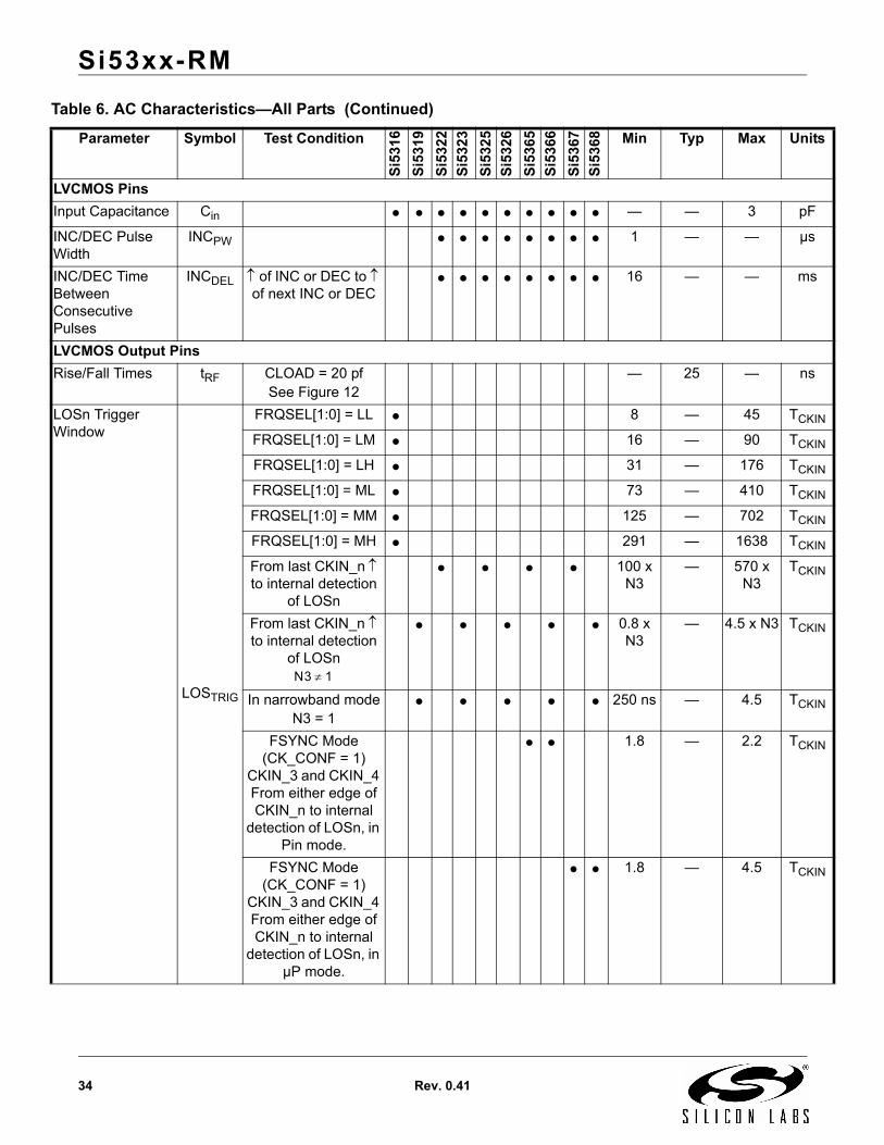
Table 6. AC Characteristics—All Parts
Parameter Symbol Test Condition
Si5
316
Si5
319
Si5
322
Si5
323
Si5
325
Si5
326
Si5
365
Si5
366
Si5
367
Si5
368 Min Typ Max Units
Input Frequency
CKNF
19.38 — 710
19.43 — 707.35 MHz
0.002 — 707.35 MHz
10 — 710 MHz
When used as frame synchronization input
— 0.008 — MHz
2 — 512 kHz
CKIN_n Input Pins
Input Duty Cycle (Minimum Pulse Width) CKNDC
Whichever is smaller (i.e., the 40% / 60 % limitation applies only
to high frequency clocks)
40 — 60 %
2 — — ns
Input Capacitance CKNCIN — — 3 pF
Input Rise/Fall Time
CKNTRF 20–80%See Figure 12
— — 11 ns
CKOUT_n Output Pins (See individual data sheets for speed grade limits)
Output Frequency (Output not configured for CMOS or tri-state)
CKOF
19.38 — 710 MHz
19.43 — 1049 MHz
0.008 — 1049 MHz
10 — 945 MHz
0.002 — 945 MHz
970 — 1134 MHz
1.2125 — 1.4 GHz
Maximum Output Frequency in CMOS Format
CKOFMC — — 212.5 MHz
Output Rise/Fall (20–80%) at 622.08 MHz
CKOTRF Output not config-ured for CMOS See
Figure 12
— 230 350 ps
Output Rise/Fall (20–80%) at 212.5 MHz CKOTRF
CMOS OutputVDD = 1.62
Cload = 5 pF
— — 8 ns
CMOS OutputVDD = 2.97
Cload = 5 pF
— — 2 ns
Output Duty Cycle Differential Uncertainty
CKODC 100 LoadLine to Line
Measured at 50% Point (not for CMOS)
— — ±40 ps
Si53xx-RM
34 Rev. 0.41
LVCMOS Pins
Input Capacitance Cin — — 3 pF
INC/DEC Pulse Width
INCPW 1 — — µs
INC/DEC Time Between Consecutive Pulses
INCDEL of INC or DEC to of next INC or DEC
16 — — ms
LVCMOS Output Pins
Rise/Fall Times tRF CLOAD = 20 pfSee Figure 12
— 25 — ns
LOSn Trigger Window
LOSTRIG
FRQSEL[1:0] = LL 8 — 45 TCKIN
FRQSEL[1:0] = LM 16 — 90 TCKIN
FRQSEL[1:0] = LH 31 — 176 TCKIN
FRQSEL[1:0] = ML 73 — 410 TCKIN
FRQSEL[1:0] = MM 125 — 702 TCKIN
FRQSEL[1:0] = MH 291 — 1638 TCKIN
From last CKIN_n to internal detection
of LOSn
100 x N3
— 570 x N3
TCKIN
From last CKIN_n to internal detection
of LOSn
0.8 x N3
— 4.5 x N3 TCKIN
In narrowband modeN3 = 1
250 ns — 4.5 TCKIN
FSYNC Mode (CK_CONF = 1)
CKIN_3 and CKIN_4 From either edge of CKIN_n to internal
detection of LOSn, in Pin mode.
1.8 — 2.2 TCKIN
FSYNC Mode (CK_CONF = 1)
CKIN_3 and CKIN_4 From either edge of CKIN_n to internal
detection of LOSn, in µP mode.
1.8 — 4.5 TCKIN
Table 6. AC Characteristics—All Parts (Continued)
Parameter Symbol Test Condition
Si5
31
6
Si5
31
9
Si5
32
2
Si5
32
3
Si5
32
5
Si5
32
6
Si5
36
5
Si5
36
6
Si5
36
7
Si5
36
8 Min Typ Max Units
N3 1
Si53xx-RM
Rev. 0.41 35
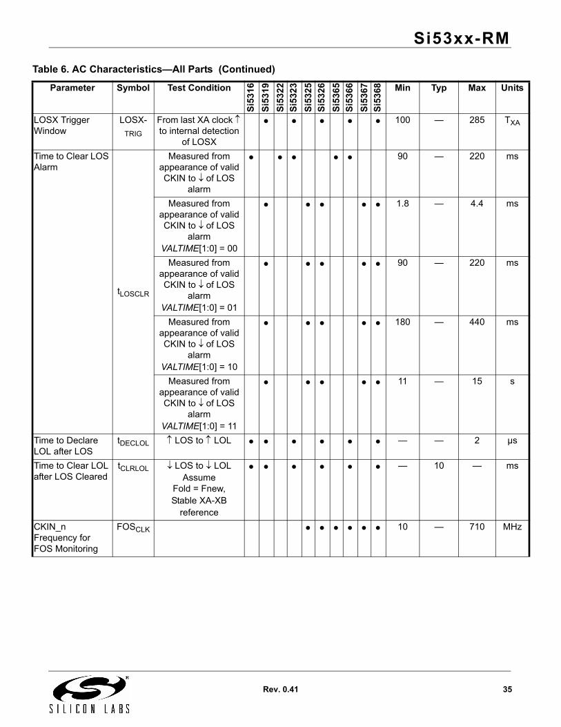
LOSX Trigger Window
LOSX-
TRIG
From last XA clock to internal detection
of LOSX
100 — 285 TXA
Time to Clear LOS Alarm
tLOSCLR
Measured from appearance of valid CKIN to of LOS
alarm
90 — 220 ms
Measured from appearance of valid CKIN to of LOS
alarmVALTIME[1:0] = 00
1.8 — 4.4 ms
Measured from appearance of valid CKIN to of LOS
alarmVALTIME[1:0] = 01
90 — 220 ms
Measured from appearance of valid CKIN to of LOS
alarmVALTIME[1:0] = 10
180 — 440 ms
Measured from appearance of valid CKIN to of LOS
alarmVALTIME[1:0] = 11
11 — 15 s
Time to Declare LOL after LOS
tDECLOL LOS to LOL — — 2 µs
Time to Clear LOL after LOS Cleared
tCLRLOL LOS to LOLAssume
Fold = Fnew, Stable XA-XB
reference
— 10 — ms
CKIN_n Frequency for FOS Monitoring
FOSCLK 10 — 710 MHz
Table 6. AC Characteristics—All Parts (Continued)
Parameter Symbol Test Condition
Si5
31
6
Si5
31
9
Si5
32
2
Si5
32
3
Si5
32
5
Si5
32
6
Si5
36
5
Si5
36
6
Si5
36
7
Si5
36
8 Min Typ Max Units
Si53xx-RM
36 Rev. 0.41
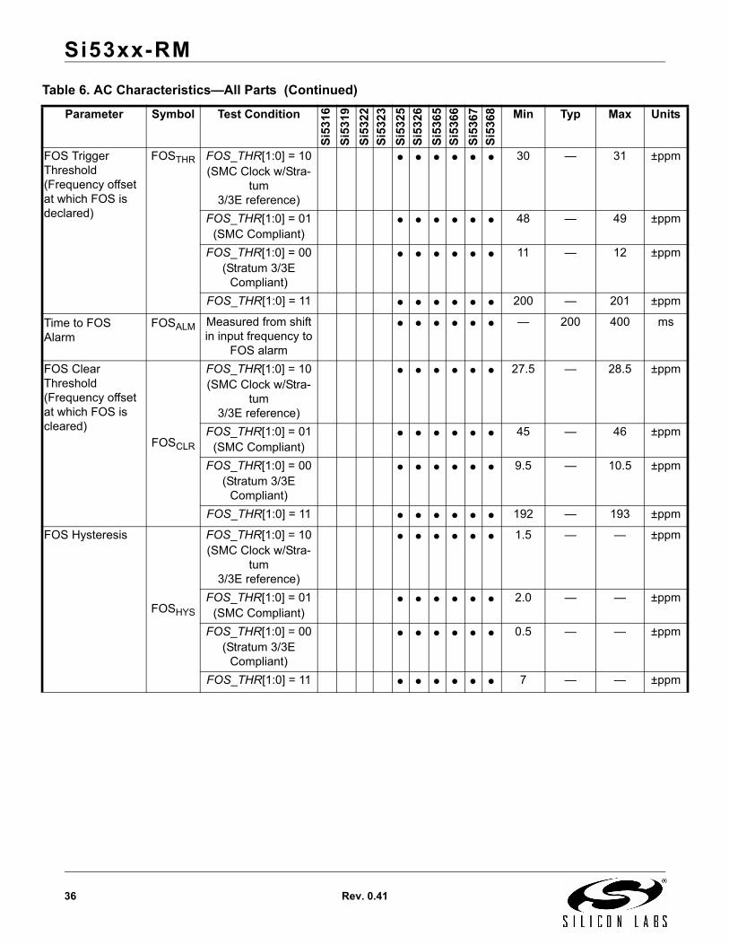
FOS Trigger Threshold (Frequency offset at which FOS is declared)
FOSTHR FOS_THR[1:0] = 10(SMC Clock w/Stra-
tum 3/3E reference)
30 — 31 ±ppm
FOS_THR[1:0] = 01(SMC Compliant)
48 — 49 ±ppm
FOS_THR[1:0] = 00(Stratum 3/3E
Compliant)
11 — 12 ±ppm
FOS_THR[1:0] = 11 200 — 201 ±ppm
Time to FOS Alarm
FOSALM Measured from shift in input frequency to
FOS alarm
— 200 400 ms
FOS Clear Threshold (Frequency offset at which FOS is cleared)
FOSCLR
FOS_THR[1:0] = 10(SMC Clock w/Stra-
tum 3/3E reference)
27.5 — 28.5 ±ppm
FOS_THR[1:0] = 01(SMC Compliant)
45 — 46 ±ppm
FOS_THR[1:0] = 00(Stratum 3/3E
Compliant)
9.5 — 10.5 ±ppm
FOS_THR[1:0] = 11 192 — 193 ±ppm
FOS Hysteresis
FOSHYS
FOS_THR[1:0] = 10(SMC Clock w/Stra-
tum 3/3E reference)
1.5 — — ±ppm
FOS_THR[1:0] = 01(SMC Compliant)
2.0 — — ±ppm
FOS_THR[1:0] = 00(Stratum 3/3E
Compliant)
0.5 — — ±ppm
FOS_THR[1:0] = 11 7 — — ±ppm
Table 6. AC Characteristics—All Parts (Continued)
Parameter Symbol Test Condition
Si5
31
6
Si5
31
9
Si5
32
2
Si5
32
3
Si5
32
5
Si5
32
6
Si5
36
5
Si5
36
6
Si5
36
7
Si5
36
8 Min Typ Max Units
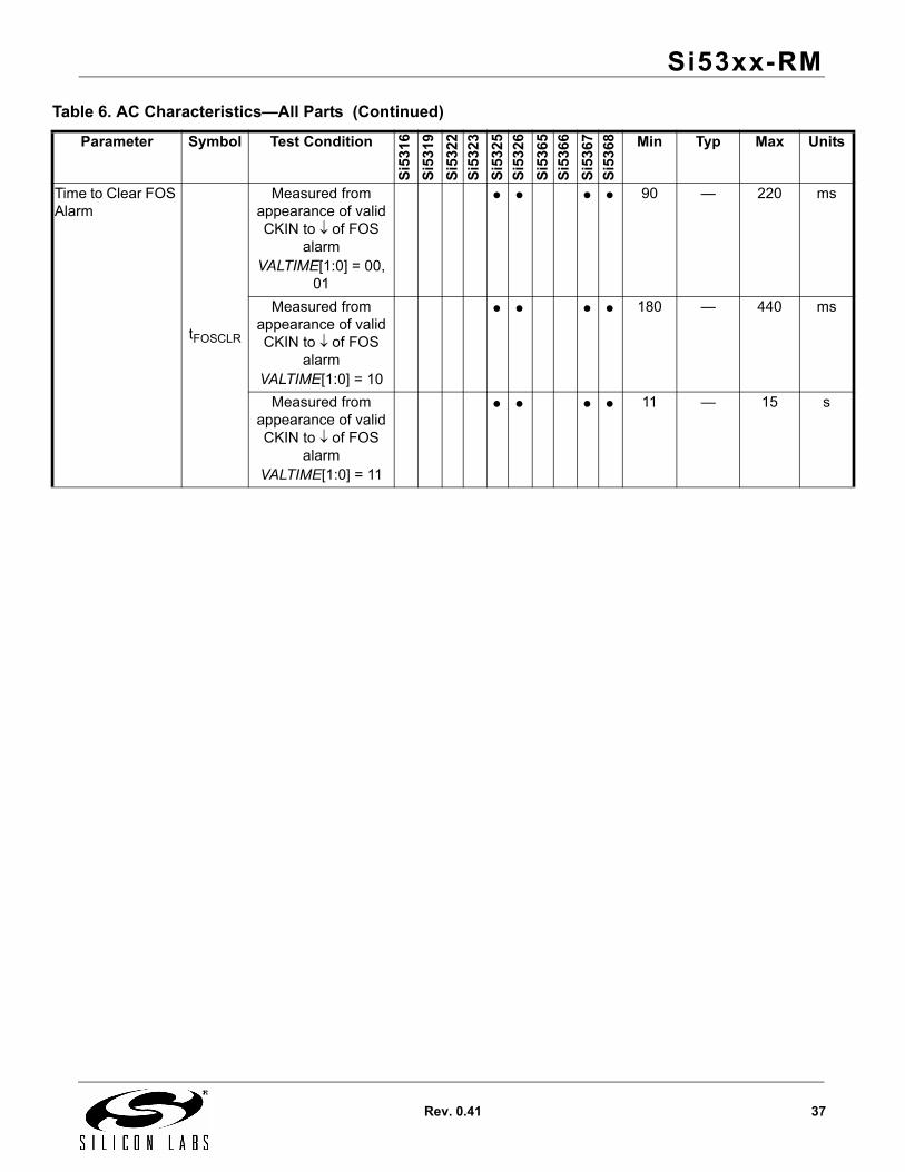
Si53xx-RM
Rev. 0.41 37
Time to Clear FOS Alarm
tFOSCLR
Measured from appearance of valid CKIN to of FOS
alarmVALTIME[1:0] = 00,
01
90 — 220 ms
Measured from appearance of valid CKIN to of FOS
alarmVALTIME[1:0] = 10
180 — 440 ms
Measured from appearance of valid CKIN to of FOS
alarmVALTIME[1:0] = 11
11 — 15 s
Table 6. AC Characteristics—All Parts (Continued)
Parameter Symbol Test Condition
Si5
31
6
Si5
31
9
Si5
32
2
Si5
32
3
Si5
32
5
Si5
32
6
Si5
36
5
Si5
36
6
Si5
36
7
Si5
36
8 Min Typ Max Units
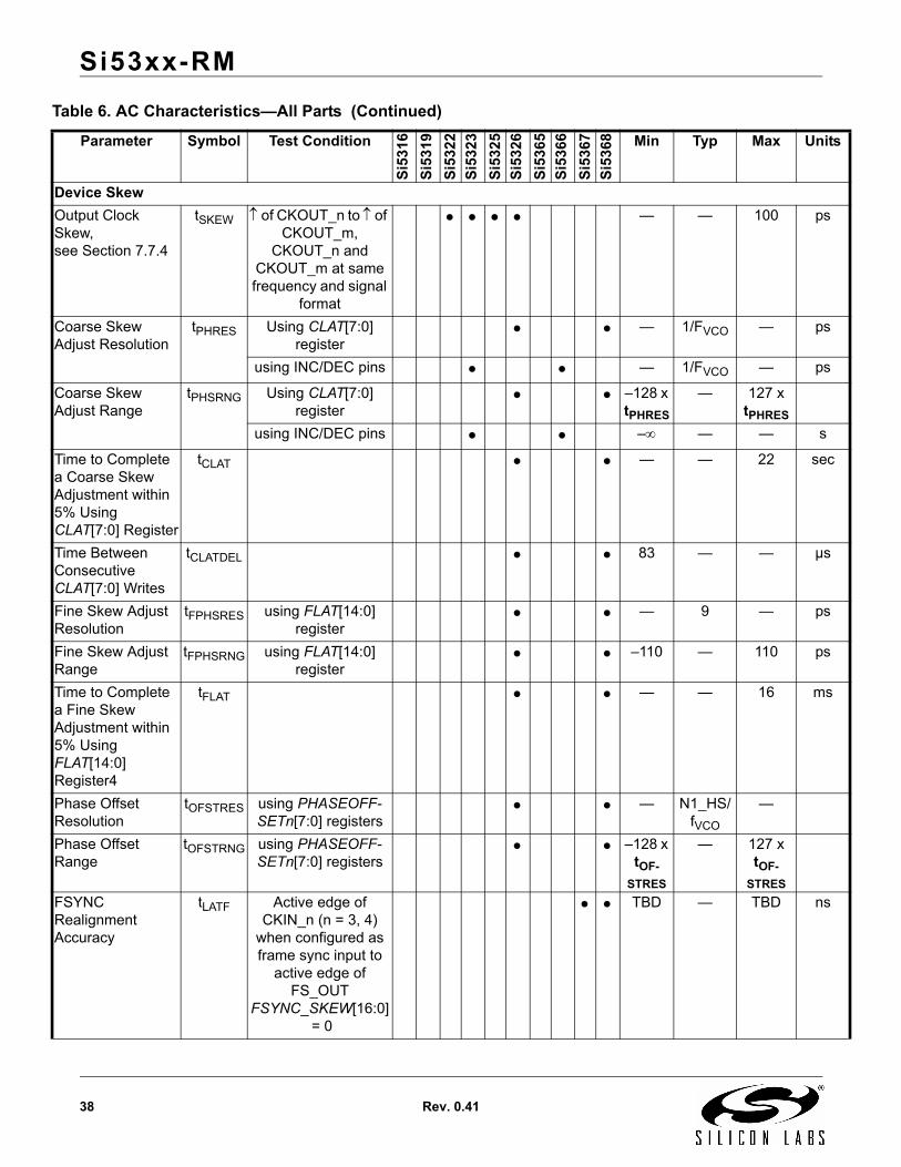
Si53xx-RM
38 Rev. 0.41
Device Skew
Output Clock Skew, see Section 7.7.4
tSKEW of CKOUT_n to of CKOUT_m,
CKOUT_n and CKOUT_m at same frequency and signal
format
— — 100 ps
Coarse Skew Adjust Resolution
tPHRES Using CLAT[7:0] register
— 1/FVCO — ps
using INC/DEC pins — 1/FVCO — ps
Coarse Skew Adjust Range
tPHSRNG Using CLAT[7:0] register
–128 x tPHRES
— 127 x tPHRES
using INC/DEC pins – — — s
Time to Complete a Coarse Skew Adjustment within 5% Using CLAT[7:0] Register
tCLAT — — 22 sec
Time Between Consecutive CLAT[7:0] Writes
tCLATDEL 83 — — µs
Fine Skew Adjust Resolution
tFPHSRES using FLAT[14:0] register
— 9 — ps
Fine Skew Adjust Range
tFPHSRNG using FLAT[14:0] register
–110 — 110 ps
Time to Complete a Fine Skew Adjustment within 5% Using FLAT[14:0] Register4
tFLAT — — 16 ms
Phase Offset Resolution
tOFSTRES using PHASEOFF-SETn[7:0] registers
— N1_HS/ fVCO
—
Phase Offset Range
tOFSTRNG using PHASEOFF-SETn[7:0] registers
–128 x tOF-
STRES
— 127 x tOF-
STRES
FSYNC Realignment Accuracy
tLATF Active edge of CKIN_n (n = 3, 4)
when configured as frame sync input to
active edge of FS_OUT
FSYNC_SKEW[16:0]= 0
TBD — TBD ns
Table 6. AC Characteristics—All Parts (Continued)
Parameter Symbol Test Condition
Si5
31
6
Si5
31
9
Si5
32
2
Si5
32
3
Si5
32
5
Si5
32
6
Si5
36
5
Si5
36
6
Si5
36
7
Si5
36
8 Min Typ Max Units
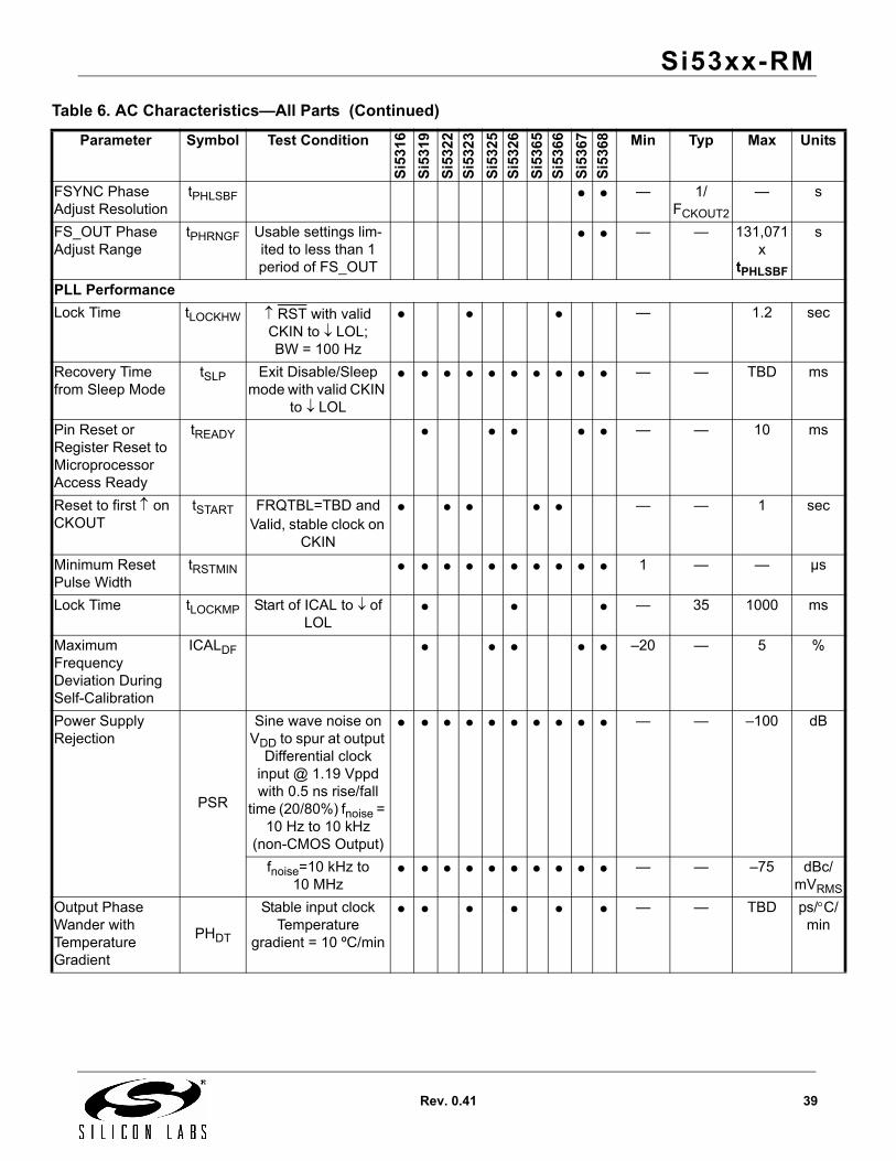
Si53xx-RM
Rev. 0.41 39
FSYNC Phase Adjust Resolution
tPHLSBF — 1/FCKOUT2
— s
FS_OUT Phase Adjust Range
tPHRNGF Usable settings lim-ited to less than 1 period of FS_OUT
— — 131,071 x
tPHLSBF
s
PLL Performance
Lock Time tLOCKHW RST with valid CKIN to LOL; BW = 100 Hz
— 1.2 sec
Recovery Time from Sleep Mode
tSLP Exit Disable/Sleep mode with valid CKIN
to LOL
— — TBD ms
Pin Reset or Register Reset to Microprocessor Access Ready
tREADY — — 10 ms
Reset to first on CKOUT
tSTART FRQTBL=TBD andValid, stable clock on
CKIN
— — 1 sec
Minimum Reset Pulse Width
tRSTMIN 1 — — µs
Lock Time tLOCKMP Start of ICAL to of LOL
— 35 1000 ms
Maximum Frequency Deviation During Self-Calibration
ICALDF –20 — 5 %
Power Supply Rejection
PSR
Sine wave noise on VDD to spur at output
Differential clock input @ 1.19 Vppd with 0.5 ns rise/fall
time (20/80%) fnoise = 10 Hz to 10 kHz
(non-CMOS Output)
— — –100 dB
fnoise=10 kHz to 10 MHz
— — –75 dBc/ mVRMS
Output Phase Wander with Temperature Gradient
PHDT
Stable input clock Temperature
gradient = 10 ºC/min
— — TBD ps/C/ min
Table 6. AC Characteristics—All Parts (Continued)
Parameter Symbol Test Condition
Si5
31
6
Si5
31
9
Si5
32
2
Si5
32
3
Si5
32
5
Si5
32
6
Si5
36
5
Si5
36
6
Si5
36
7
Si5
36
8 Min Typ Max Units
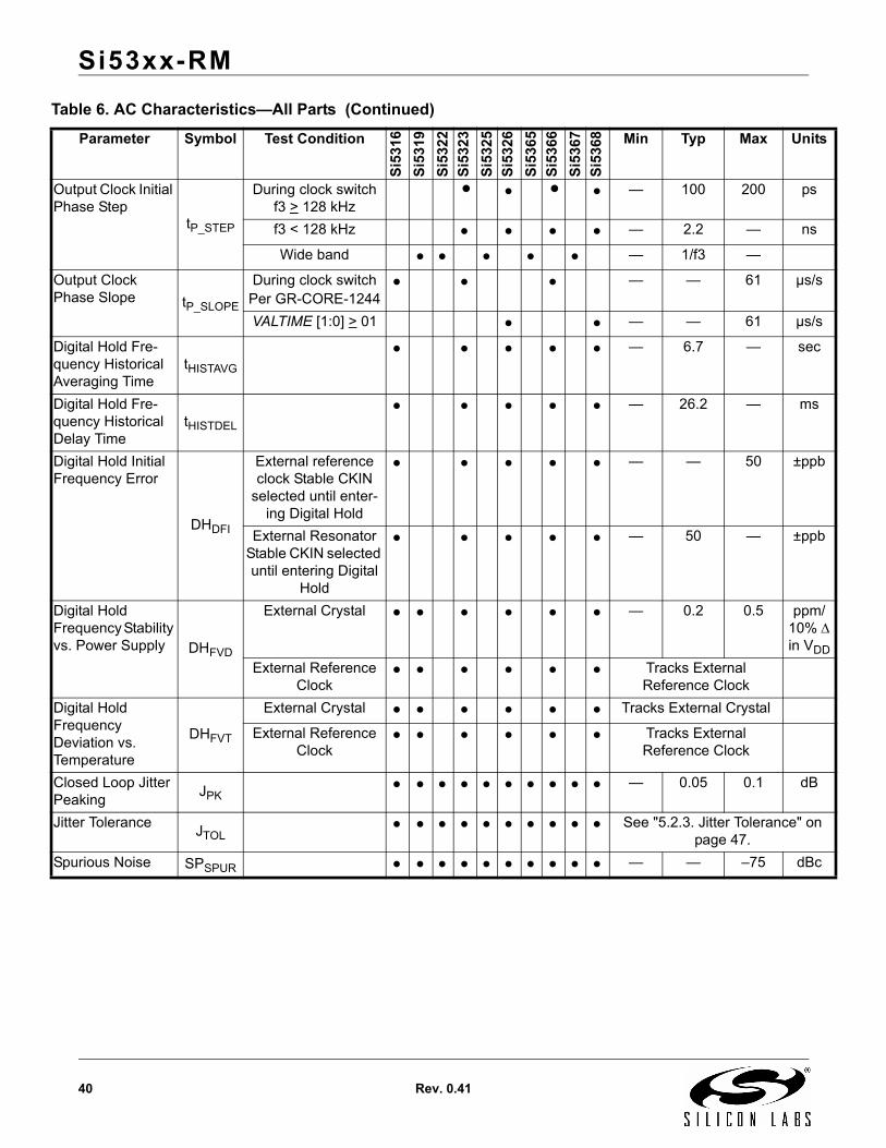
Si53xx-RM
40 Rev. 0.41
Output Clock Initial Phase Step
tP_STEP
During clock switch f3 > 128 kHz
— 100 200 ps
f3 < 128 kHz — 2.2 — ns
Wide band — 1/f3 —
Output Clock Phase Slope tP_SLOPE
During clock switchPer GR-CORE-1244
— — 61 µs/s
VALTIME [1:0] > 01 — — 61 µs/s
Digital Hold Fre-quency Historical Averaging Time
tHISTAVG
— 6.7 — sec
Digital Hold Fre-quency Historical Delay Time
tHISTDEL
— 26.2 — ms
Digital Hold Initial Frequency Error
DHDFI
External reference clock Stable CKIN
selected until enter-ing Digital Hold
— — 50 ±ppb
External Resonator Stable CKIN selected until entering Digital
Hold
— 50 — ±ppb
Digital Hold Frequency Stability vs. Power Supply DHFVD
External Crystal — 0.2 0.5 ppm/ 10% in VDD
External Reference Clock
Tracks External Reference Clock
Digital Hold Frequency Deviation vs. Temperature
DHFVT
External Crystal Tracks External Crystal
External Reference Clock
Tracks External Reference Clock
Closed Loop Jitter Peaking
JPK — 0.05 0.1 dB
Jitter ToleranceJTOL
See "5.2.3. Jitter Tolerance" on page 47.
Spurious Noise SPSPUR — — –75 dBc
Table 6. AC Characteristics—All Parts (Continued)
Parameter Symbol Test Condition
Si5
31
6
Si5
31
9
Si5
32
2
Si5
32
3
Si5
32
5
Si5
32
6
Si5
36
5
Si5
36
6
Si5
36
7
Si5
36
8 Min Typ Max Units
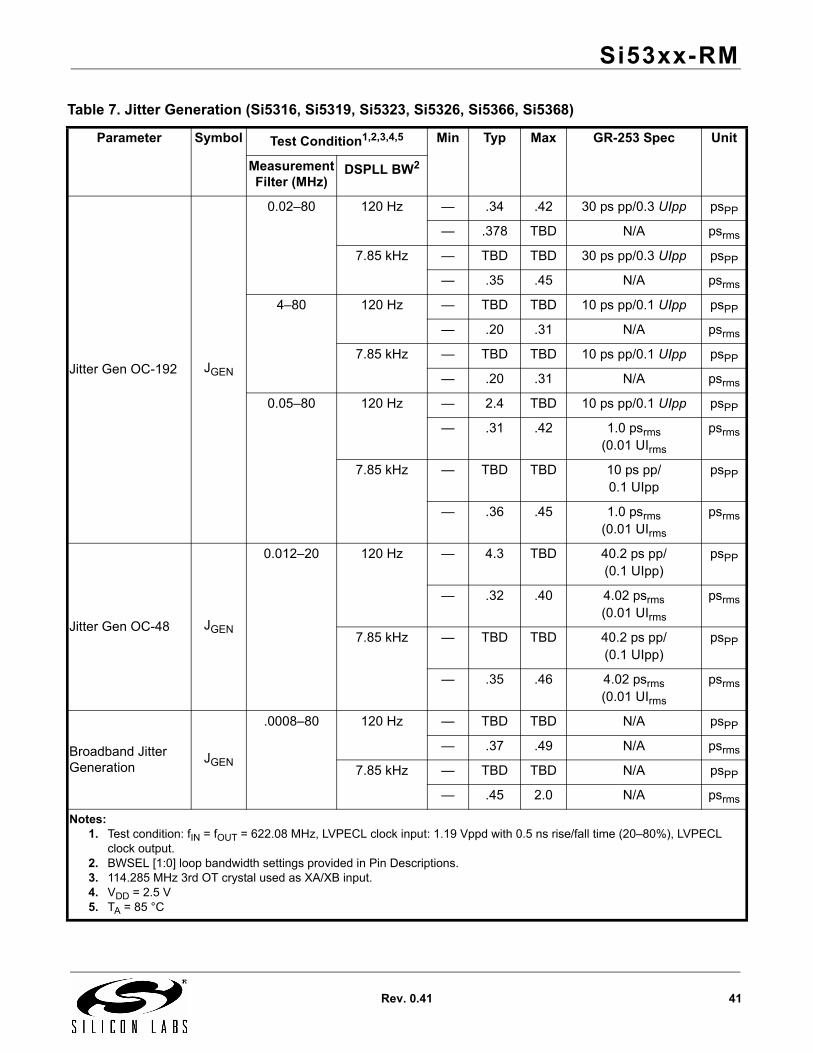
Si53xx-RM
Rev. 0.41 41
Table 7. Jitter Generation (Si5316, Si5319, Si5323, Si5326, Si5366, Si5368)
Parameter Symbol Test Condition1,2,3,4,5 Min Typ Max GR-253 Spec Unit
Measurement Filter (MHz)
DSPLL BW2
Jitter Gen OC-192 JGEN
0.02–80 120 Hz — .34 .42 30 ps pp/0.3 UIpp psPP
— .378 TBD N/A psrms
7.85 kHz — TBD TBD 30 ps pp/0.3 UIpp psPP
— .35 .45 N/A psrms
4–80 120 Hz — TBD TBD 10 ps pp/0.1 UIpp psPP
— .20 .31 N/A psrms
7.85 kHz — TBD TBD 10 ps pp/0.1 UIpp psPP
— .20 .31 N/A psrms
0.05–80 120 Hz — 2.4 TBD 10 ps pp/0.1 UIpp psPP
— .31 .42 1.0 psrms(0.01 UIrms
psrms
7.85 kHz — TBD TBD 10 ps pp/0.1 UIpp
psPP
— .36 .45 1.0 psrms(0.01 UIrms
psrms
Jitter Gen OC-48 JGEN
0.012–20 120 Hz — 4.3 TBD 40.2 ps pp/(0.1 UIpp)
psPP
— .32 .40 4.02 psrms(0.01 UIrms
psrms
7.85 kHz — TBD TBD 40.2 ps pp/(0.1 UIpp)
psPP
— .35 .46 4.02 psrms(0.01 UIrms
psrms
Broadband Jitter Generation
JGEN
.0008–80 120 Hz — TBD TBD N/A psPP
— .37 .49 N/A psrms
7.85 kHz — TBD TBD N/A psPP
— .45 2.0 N/A psrms
Notes:1. Test condition: fIN = fOUT = 622.08 MHz, LVPECL clock input: 1.19 Vppd with 0.5 ns rise/fall time (20–80%), LVPECL
clock output.2. BWSEL [1:0] loop bandwidth settings provided in Pin Descriptions.3. 114.285 MHz 3rd OT crystal used as XA/XB input.4. VDD = 2.5 V5. TA = 85 °C
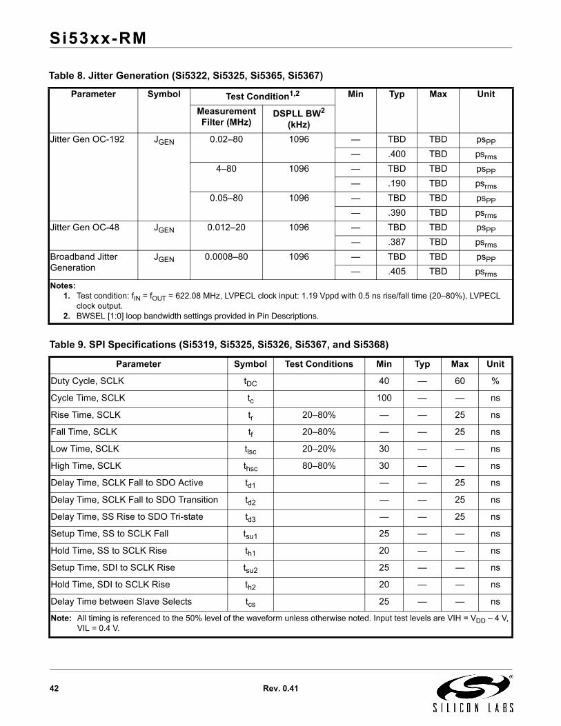
Si53xx-RM
42 Rev. 0.41
Table 8. Jitter Generation (Si5322, Si5325, Si5365, Si5367)
Parameter Symbol Test Condition1,2 Min Typ Max Unit
Measurement Filter (MHz)
DSPLL BW2 (kHz)
Jitter Gen OC-192 JGEN 0.02–80 1096 — TBD TBD psPP
— .400 TBD psrms
4–80 1096 — TBD TBD psPP
— .190 TBD psrms
0.05–80 1096 — TBD TBD psPP
— .390 TBD psrms
Jitter Gen OC-48 JGEN 0.012–20 1096 — TBD TBD psPP
— .387 TBD psrms
Broadband Jitter Generation
JGEN 0.0008–80 1096 — TBD TBD psPP
— .405 TBD psrms
Notes:1. Test condition: fIN = fOUT = 622.08 MHz, LVPECL clock input: 1.19 Vppd with 0.5 ns rise/fall time (20–80%), LVPECL
clock output.2. BWSEL [1:0] loop bandwidth settings provided in Pin Descriptions.
Table 9. SPI Specifications (Si5319, Si5325, Si5326, Si5367, and Si5368)
Parameter Symbol Test Conditions Min Typ Max Unit
Duty Cycle, SCLK tDC 40 — 60 %
Cycle Time, SCLK tc 100 — — ns
Rise Time, SCLK tr 20–80% — — 25 ns
Fall Time, SCLK tf 20–80% — — 25 ns
Low Time, SCLK tlsc 20–20% 30 — — ns
High Time, SCLK thsc 80–80% 30 — — ns
Delay Time, SCLK Fall to SDO Active td1 — — 25 ns
Delay Time, SCLK Fall to SDO Transition td2 — — 25 ns
Delay Time, SS Rise to SDO Tri-state td3 — — 25 ns
Setup Time, SS to SCLK Fall tsu1 25 — — ns
Hold Time, SS to SCLK Rise th1 20 — — ns
Setup Time, SDI to SCLK Rise tsu2 25 — — ns
Hold Time, SDI to SCLK Rise th2 20 — — ns
Delay Time between Slave Selects tcs 25 — — ns
Note: All timing is referenced to the 50% level of the waveform unless otherwise noted. Input test levels are VIH = VDD – 4 V, VIL = 0.4 V.
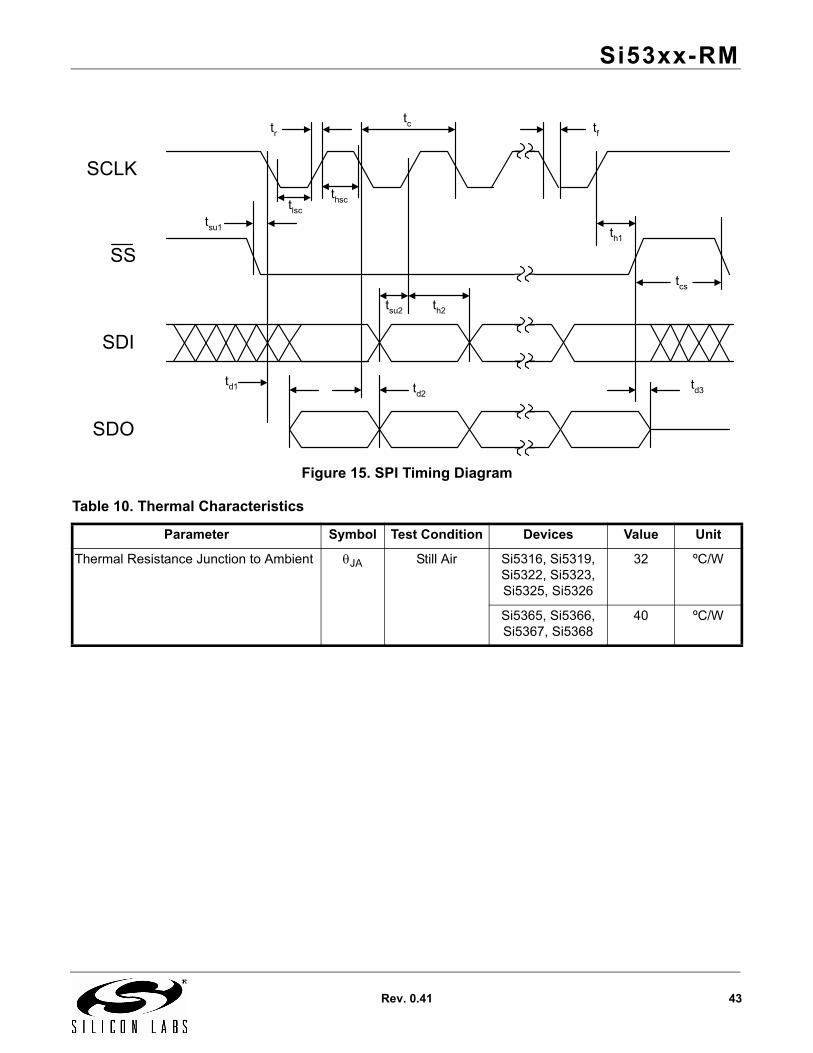
Si53xx-RM
Rev. 0.41 43
Figure 15. SPI Timing Diagram
Table 10. Thermal Characteristics
Parameter Symbol Test Condition Devices Value Unit
Thermal Resistance Junction to Ambient JA Still Air Si5316, Si5319, Si5322, Si5323, Si5325, Si5326
32 ºC/W
Si5365, Si5366, Si5367, Si5368
40 ºC/W
SCLK
SS
SDI
th1
td3
SDO
td1 td2
tsu1
tr tftc
tsu2 th2
tcs
tlsc
thsc
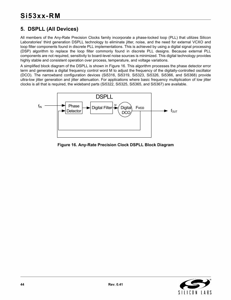
Si53xx-RM
44 Rev. 0.41
5. DSPLL (All Devices)
All members of the Any-Rate Precision Clocks family incorporate a phase-locked loop (PLL) that utilizes SiliconLaboratories' third generation DSPLL technology to eliminate jitter, noise, and the need for external VCXO andloop filter components found in discrete PLL implementations. This is achieved by using a digital signal processing(DSP) algorithm to replace the loop filter commonly found in discrete PLL designs. Because external PLLcomponents are not required, sensitivity to board-level noise sources is minimized. This digital technology provideshighly stable and consistent operation over process, temperature, and voltage variations.
A simplified block diagram of the DSPLL is shown in Figure 16. This algorithm processes the phase detector errorterm and generates a digital frequency control word M to adjust the frequency of the digitally-controlled oscillator(DCO). The narrowband configuration devices (Si5316, Si5319, Si5323, Si5326, Si5366, and Si5368) provideultra-low jitter generation and jitter attenuation. For applications where basic frequency multiplication of low jitterclocks is all that is required, the wideband parts (Si5322, Si5325, Si5365, and Si5367) are available.
Figure 16. Any-Rate Precision Clock DSPLL Block Diagram
fIN
DSPLL
PhaseDetector
DigitalDCO
Digital Filter FvcoM
fOUT
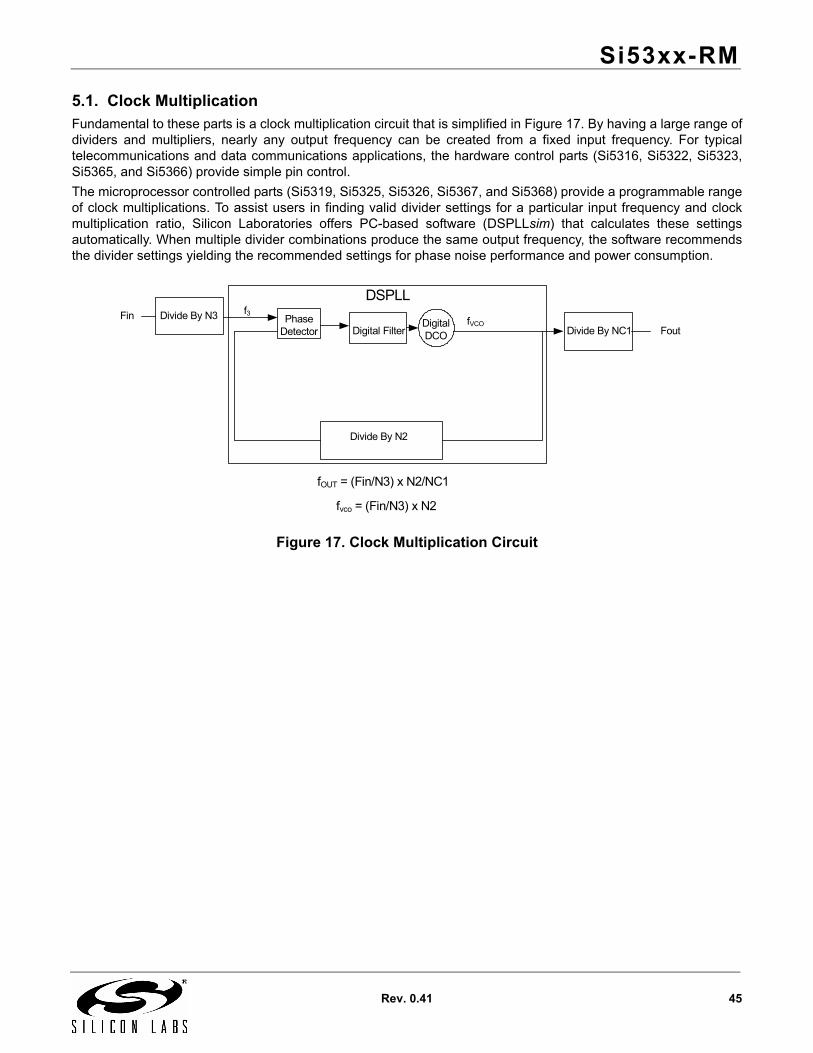
Si53xx-RM
Rev. 0.41 45
5.1. Clock MultiplicationFundamental to these parts is a clock multiplication circuit that is simplified in Figure 17. By having a large range ofdividers and multipliers, nearly any output frequency can be created from a fixed input frequency. For typicaltelecommunications and data communications applications, the hardware control parts (Si5316, Si5322, Si5323,Si5365, and Si5366) provide simple pin control.
The microprocessor controlled parts (Si5319, Si5325, Si5326, Si5367, and Si5368) provide a programmable rangeof clock multiplications. To assist users in finding valid divider settings for a particular input frequency and clockmultiplication ratio, Silicon Laboratories offers PC-based software (DSPLLsim) that calculates these settingsautomatically. When multiple divider combinations produce the same output frequency, the software recommendsthe divider settings yielding the recommended settings for phase noise performance and power consumption.
Figure 17. Clock Multiplication Circuit
Fin
DSPLL
PhaseDetector
DigitalDCODigital Filter
Divide By N2
Divide By N3
Divide By NC1 Fout
fOUT = (Fin/N3) x N2/NC1
fvco = (Fin/N3) x N2
f3fVCO
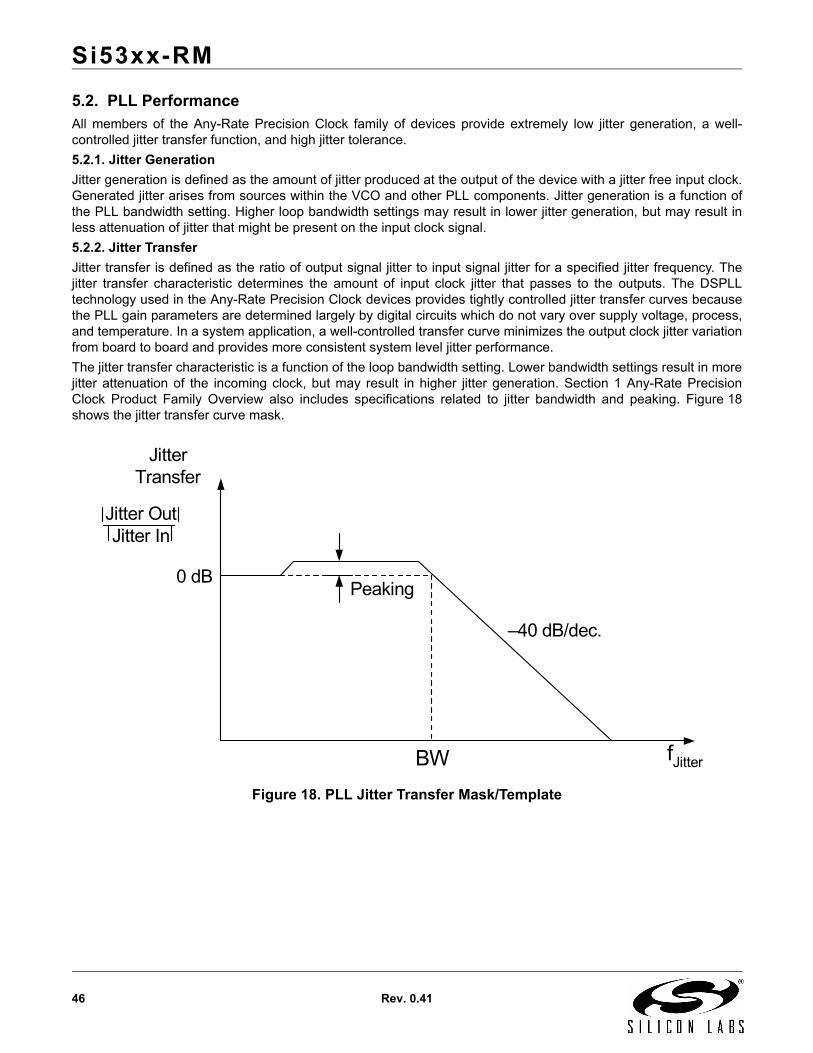
Si53xx-RM
46 Rev. 0.41
5.2. PLL PerformanceAll members of the Any-Rate Precision Clock family of devices provide extremely low jitter generation, a well-controlled jitter transfer function, and high jitter tolerance.
5.2.1. Jitter Generation
Jitter generation is defined as the amount of jitter produced at the output of the device with a jitter free input clock.Generated jitter arises from sources within the VCO and other PLL components. Jitter generation is a function ofthe PLL bandwidth setting. Higher loop bandwidth settings may result in lower jitter generation, but may result inless attenuation of jitter that might be present on the input clock signal.
5.2.2. Jitter Transfer
Jitter transfer is defined as the ratio of output signal jitter to input signal jitter for a specified jitter frequency. Thejitter transfer characteristic determines the amount of input clock jitter that passes to the outputs. The DSPLLtechnology used in the Any-Rate Precision Clock devices provides tightly controlled jitter transfer curves becausethe PLL gain parameters are determined largely by digital circuits which do not vary over supply voltage, process,and temperature. In a system application, a well-controlled transfer curve minimizes the output clock jitter variationfrom board to board and provides more consistent system level jitter performance.
The jitter transfer characteristic is a function of the loop bandwidth setting. Lower bandwidth settings result in morejitter attenuation of the incoming clock, but may result in higher jitter generation. Section 1 Any-Rate PrecisionClock Product Family Overview also includes specifications related to jitter bandwidth and peaking. Figure 18shows the jitter transfer curve mask.
Figure 18. PLL Jitter Transfer Mask/Template
JitterTransfer
0 dB
BW fJitter
Peaking
–40 dB/dec.
Jitter OutJitter In
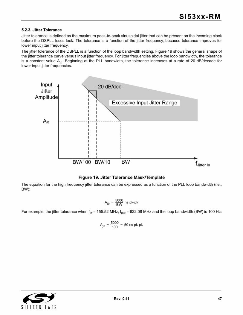
Si53xx-RM
Rev. 0.41 47
5.2.3. Jitter Tolerance
Jitter tolerance is defined as the maximum peak-to-peak sinusoidal jitter that can be present on the incoming clockbefore the DSPLL loses lock. The tolerance is a function of the jitter frequency, because tolerance improves forlower input jitter frequency.
The jitter tolerance of the DSPLL is a function of the loop bandwidth setting. Figure 19 shows the general shape ofthe jitter tolerance curve versus input jitter frequency. For jitter frequencies above the loop bandwidth, the toleranceis a constant value Aj0. Beginning at the PLL bandwidth, the tolerance increases at a rate of 20 dB/decade forlower input jitter frequencies.
Figure 19. Jitter Tolerance Mask/Template
The equation for the high frequency jitter tolerance can be expressed as a function of the PLL loop bandwidth (i.e.,BW):
For example, the jitter tolerance when fin = 155.52 MHz, fout = 622.08 MHz and the loop bandwidth (BW) is 100 Hz:
InputJitter
Amplitude
Aj0
–20 dB/dec.
fJitter In
Excessive Input Jitter Range
BW/100 BW/10 BW
Aj05000BW
------------- ns pk-pk=
Aj05000100
------------- 50 ns pk-pk= =
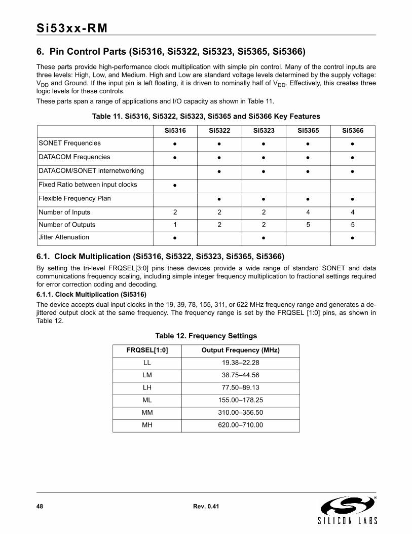
Si53xx-RM
48 Rev. 0.41
6. Pin Control Parts (Si5316, Si5322, Si5323, Si5365, Si5366)
These parts provide high-performance clock multiplication with simple pin control. Many of the control inputs arethree levels: High, Low, and Medium. High and Low are standard voltage levels determined by the supply voltage:VDD and Ground. If the input pin is left floating, it is driven to nominally half of VDD. Effectively, this creates threelogic levels for these controls.
These parts span a range of applications and I/O capacity as shown in Table 11.
6.1. Clock Multiplication (Si5316, Si5322, Si5323, Si5365, Si5366)By setting the tri-level FRQSEL[3:0] pins these devices provide a wide range of standard SONET and datacommunications frequency scaling, including simple integer frequency multiplication to fractional settings requiredfor error correction coding and decoding.
6.1.1. Clock Multiplication (Si5316)
The device accepts dual input clocks in the 19, 39, 78, 155, 311, or 622 MHz frequency range and generates a de-jittered output clock at the same frequency. The frequency range is set by the FRQSEL [1:0] pins, as shown inTable 12.
Table 11. Si5316, Si5322, Si5323, Si5365 and Si5366 Key Features
Si5316 Si5322 Si5323 Si5365 Si5366
SONET Frequencies
DATACOM Frequencies
DATACOM/SONET internetworking
Fixed Ratio between input clocks
Flexible Frequency Plan
Number of Inputs 2 2 2 4 4
Number of Outputs 1 2 2 5 5
Jitter Attenuation
Table 12. Frequency Settings
FRQSEL[1:0] Output Frequency (MHz)
LL 19.38–22.28
LM 38.75–44.56
LH 77.50–89.13
ML 155.00–178.25
MM 310.00–356.50
MH 620.00–710.00
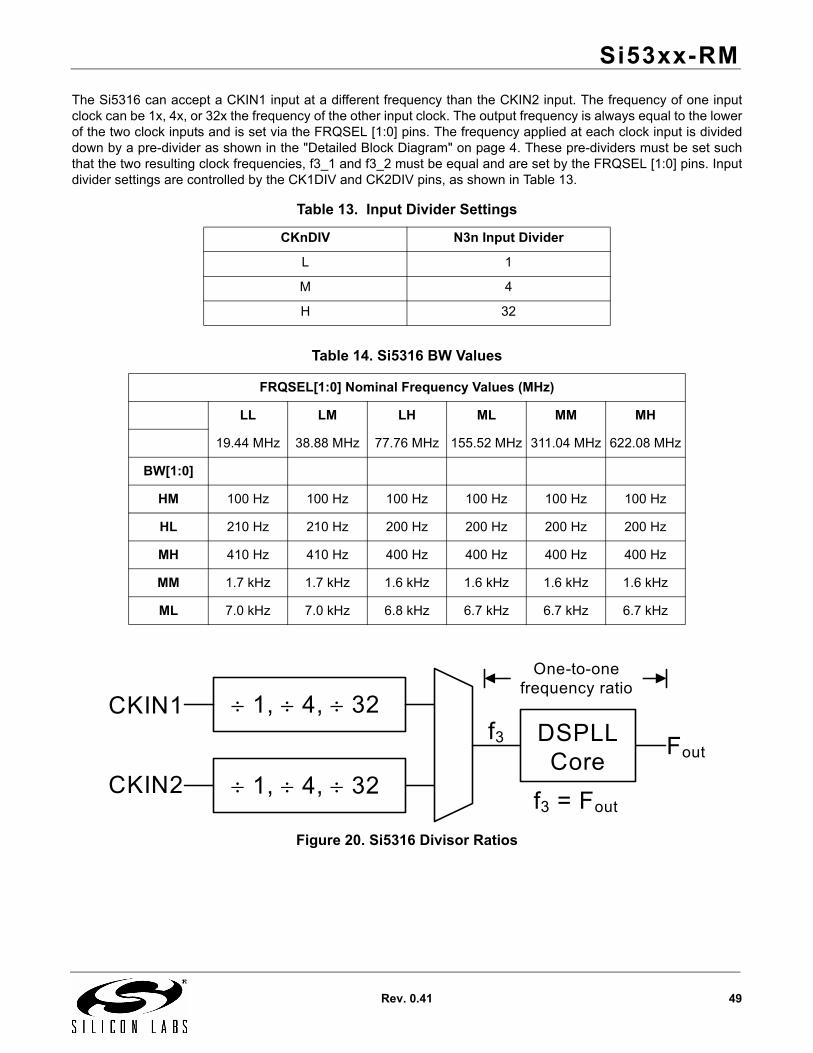
Si53xx-RM
Rev. 0.41 49
The Si5316 can accept a CKIN1 input at a different frequency than the CKIN2 input. The frequency of one inputclock can be 1x, 4x, or 32x the frequency of the other input clock. The output frequency is always equal to the lowerof the two clock inputs and is set via the FRQSEL [1:0] pins. The frequency applied at each clock input is divideddown by a pre-divider as shown in the "Detailed Block Diagram" on page 4. These pre-dividers must be set suchthat the two resulting clock frequencies, f3_1 and f3_2 must be equal and are set by the FRQSEL [1:0] pins. Inputdivider settings are controlled by the CK1DIV and CK2DIV pins, as shown in Table 13.
Figure 20. Si5316 Divisor Ratios
Table 13. Input Divider Settings
CKnDIV N3n Input Divider
L 1
M 4
H 32
Table 14. Si5316 BW Values
FRQSEL[1:0] Nominal Frequency Values (MHz)
LL LM LH ML MM MH
19.44 MHz 38.88 MHz 77.76 MHz 155.52 MHz 311.04 MHz 622.08 MHz
BW[1:0]
HM 100 Hz 100 Hz 100 Hz 100 Hz 100 Hz 100 Hz
HL 210 Hz 210 Hz 200 Hz 200 Hz 200 Hz 200 Hz
MH 410 Hz 410 Hz 400 Hz 400 Hz 400 Hz 400 Hz
MM 1.7 kHz 1.7 kHz 1.6 kHz 1.6 kHz 1.6 kHz 1.6 kHz
ML 7.0 kHz 7.0 kHz 6.8 kHz 6.7 kHz 6.7 kHz 6.7 kHz
1, 4, 32
1, 4, 32
CKIN1
CKIN2
DSPLLCore
Fout
f3 = Fout
f3
One-to-one frequency ratio
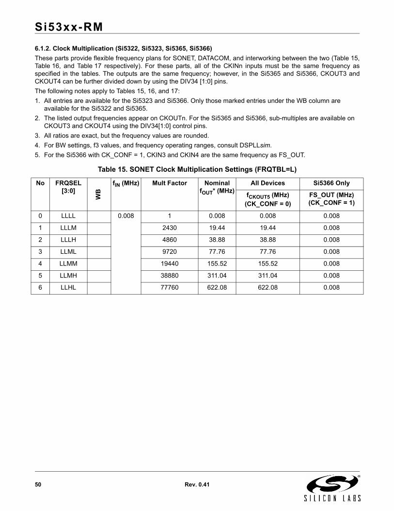
Si53xx-RM
50 Rev. 0.41
6.1.2. Clock Multiplication (Si5322, Si5323, Si5365, Si5366)
These parts provide flexible frequency plans for SONET, DATACOM, and interworking between the two (Table 15,Table 16, and Table 17 respectively). For these parts, all of the CKINn inputs must be the same frequency asspecified in the tables. The outputs are the same frequency; however, in the Si5365 and Si5366, CKOUT3 andCKOUT4 can be further divided down by using the DIV34 [1:0] pins.
The following notes apply to Tables 15, 16, and 17:
1. All entries are available for the Si5323 and Si5366. Only those marked entries under the WB column are available for the Si5322 and Si5365.
2. The listed output frequencies appear on CKOUTn. For the Si5365 and Si5366, sub-multiples are available on CKOUT3 and CKOUT4 using the DIV34[1:0] control pins.
3. All ratios are exact, but the frequency values are rounded.
4. For BW settings, f3 values, and frequency operating ranges, consult DSPLLsim.
5. For the Si5366 with CK_CONF = 1, CKIN3 and CKIN4 are the same frequency as FS_OUT.
Table 15. SONET Clock Multiplication Settings (FRQTBL=L)
No FRQSEL[3:0]
WB
fIN (MHz) Mult Factor Nominal fOUT* (MHz)
All Devices Si5366 Only
fCKOUT5 (MHz)(CK_CONF = 0)
FS_OUT (MHz)(CK_CONF = 1)
0 LLLL 0.008 1 0.008 0.008 0.008
1 LLLM 2430 19.44 19.44 0.008
2 LLLH 4860 38.88 38.88 0.008
3 LLML 9720 77.76 77.76 0.008
4 LLMM 19440 155.52 155.52 0.008
5 LLMH 38880 311.04 311.04 0.008
6 LLHL 77760 622.08 622.08 0.008
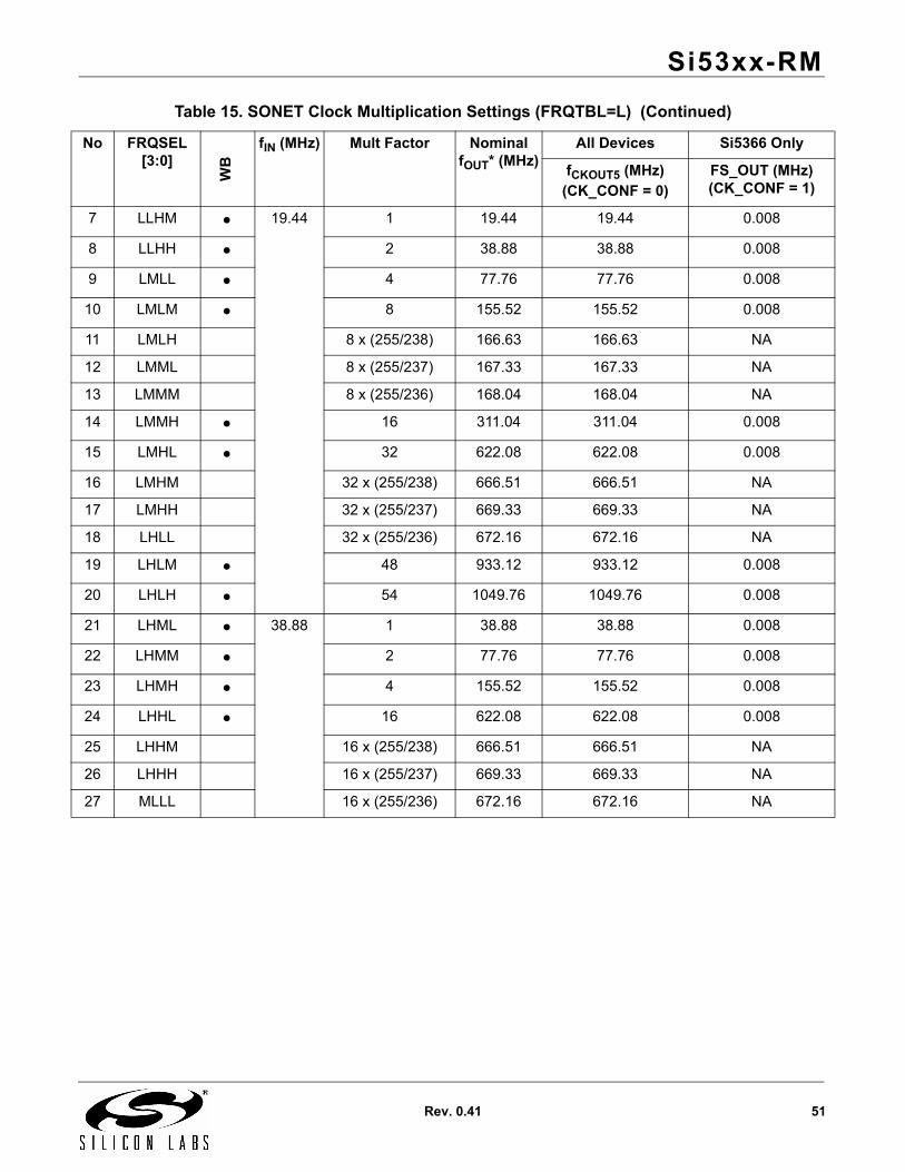
Si53xx-RM
Rev. 0.41 51
7 LLHM 19.44 1 19.44 19.44 0.008
8 LLHH 2 38.88 38.88 0.008
9 LMLL 4 77.76 77.76 0.008
10 LMLM 8 155.52 155.52 0.008
11 LMLH 8 x (255/238) 166.63 166.63 NA
12 LMML 8 x (255/237) 167.33 167.33 NA
13 LMMM 8 x (255/236) 168.04 168.04 NA
14 LMMH 16 311.04 311.04 0.008
15 LMHL 32 622.08 622.08 0.008
16 LMHM 32 x (255/238) 666.51 666.51 NA
17 LMHH 32 x (255/237) 669.33 669.33 NA
18 LHLL 32 x (255/236) 672.16 672.16 NA
19 LHLM 48 933.12 933.12 0.008
20 LHLH 54 1049.76 1049.76 0.008
21 LHML 38.88 1 38.88 38.88 0.008
22 LHMM 2 77.76 77.76 0.008
23 LHMH 4 155.52 155.52 0.008
24 LHHL 16 622.08 622.08 0.008
25 LHHM 16 x (255/238) 666.51 666.51 NA
26 LHHH 16 x (255/237) 669.33 669.33 NA
27 MLLL 16 x (255/236) 672.16 672.16 NA
Table 15. SONET Clock Multiplication Settings (FRQTBL=L) (Continued)
No FRQSEL[3:0]
WB
fIN (MHz) Mult Factor Nominal fOUT* (MHz)
All Devices Si5366 Only
fCKOUT5 (MHz)(CK_CONF = 0)
FS_OUT (MHz)(CK_CONF = 1)
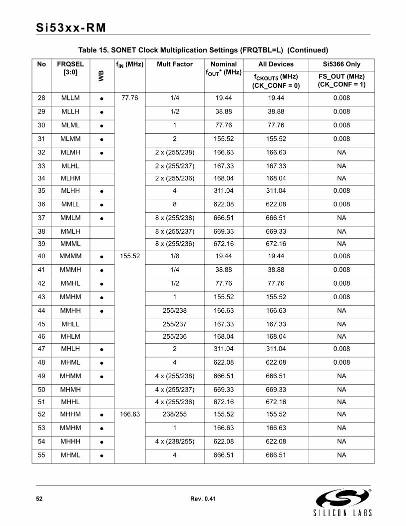
Si53xx-RM
52 Rev. 0.41
28 MLLM 77.76 1/4 19.44 19.44 0.008
29 MLLH 1/2 38.88 38.88 0.008
30 MLML 1 77.76 77.76 0.008
31 MLMM 2 155.52 155.52 0.008
32 MLMH 2 x (255/238) 166.63 166.63 NA
33 MLHL 2 x (255/237) 167.33 167.33 NA
34 MLHM 2 x (255/236) 168.04 168.04 NA
35 MLHH 4 311.04 311.04 0.008
36 MMLL 8 622.08 622.08 0.008
37 MMLM 8 x (255/238) 666.51 666.51 NA
38 MMLH 8 x (255/237) 669.33 669.33 NA
39 MMML 8 x (255/236) 672.16 672.16 NA
40 MMMM 155.52 1/8 19.44 19.44 0.008
41 MMMH 1/4 38.88 38.88 0.008
42 MMHL 1/2 77.76 77.76 0.008
43 MMHM 1 155.52 155.52 0.008
44 MMHH 255/238 166.63 166.63 NA
45 MHLL 255/237 167.33 167.33 NA
46 MHLM 255/236 168.04 168.04 NA
47 MHLH 2 311.04 311.04 0.008
48 MHML 4 622.08 622.08 0.008
49 MHMM 4 x (255/238) 666.51 666.51 NA
50 MHMH 4 x (255/237) 669.33 669.33 NA
51 MHHL 4 x (255/236) 672.16 672.16 NA
52 MHHM 166.63 238/255 155.52 155.52 NA
53 MMHM 1 166.63 166.63 NA
54 MHHH 4 x (238/255) 622.08 622.08 NA
55 MHML 4 666.51 666.51 NA
Table 15. SONET Clock Multiplication Settings (FRQTBL=L) (Continued)
No FRQSEL[3:0]
WB
fIN (MHz) Mult Factor Nominal fOUT* (MHz)
All Devices Si5366 Only
fCKOUT5 (MHz)(CK_CONF = 0)
FS_OUT (MHz)(CK_CONF = 1)
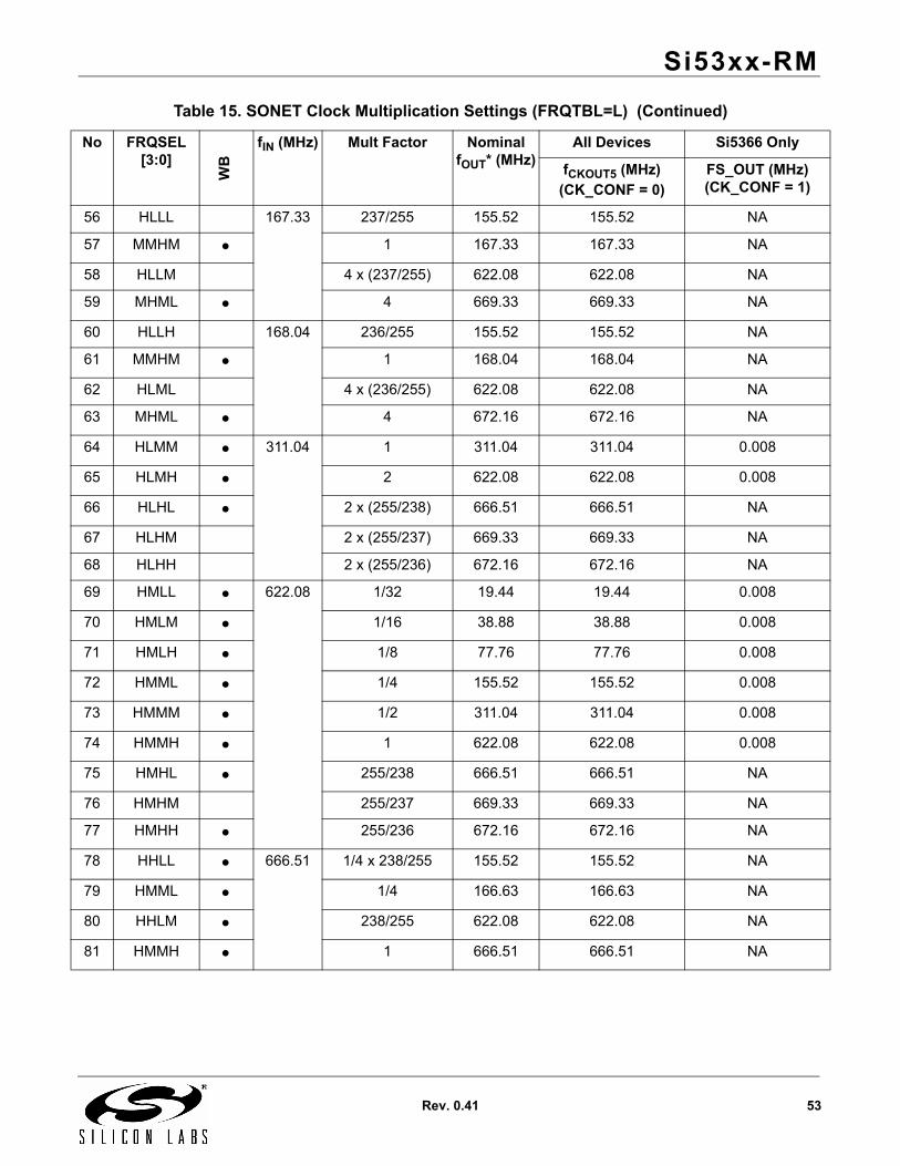
Si53xx-RM
Rev. 0.41 53
56 HLLL 167.33 237/255 155.52 155.52 NA
57 MMHM 1 167.33 167.33 NA
58 HLLM 4 x (237/255) 622.08 622.08 NA
59 MHML 4 669.33 669.33 NA
60 HLLH 168.04 236/255 155.52 155.52 NA
61 MMHM 1 168.04 168.04 NA
62 HLML 4 x (236/255) 622.08 622.08 NA
63 MHML 4 672.16 672.16 NA
64 HLMM 311.04 1 311.04 311.04 0.008
65 HLMH 2 622.08 622.08 0.008
66 HLHL 2 x (255/238) 666.51 666.51 NA
67 HLHM 2 x (255/237) 669.33 669.33 NA
68 HLHH 2 x (255/236) 672.16 672.16 NA
69 HMLL 622.08 1/32 19.44 19.44 0.008
70 HMLM 1/16 38.88 38.88 0.008
71 HMLH 1/8 77.76 77.76 0.008
72 HMML 1/4 155.52 155.52 0.008
73 HMMM 1/2 311.04 311.04 0.008
74 HMMH 1 622.08 622.08 0.008
75 HMHL 255/238 666.51 666.51 NA
76 HMHM 255/237 669.33 669.33 NA
77 HMHH 255/236 672.16 672.16 NA
78 HHLL 666.51 1/4 x 238/255 155.52 155.52 NA
79 HMML 1/4 166.63 166.63 NA
80 HHLM 238/255 622.08 622.08 NA
81 HMMH 1 666.51 666.51 NA
Table 15. SONET Clock Multiplication Settings (FRQTBL=L) (Continued)
No FRQSEL[3:0]
WB
fIN (MHz) Mult Factor Nominal fOUT* (MHz)
All Devices Si5366 Only
fCKOUT5 (MHz)(CK_CONF = 0)
FS_OUT (MHz)(CK_CONF = 1)
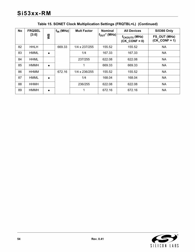
Si53xx-RM
54 Rev. 0.41
82 HHLH 669.33 1/4 x 237/255 155.52 155.52 NA
83 HMML 1/4 167.33 167.33 NA
84 HHML 237/255 622.08 622.08 NA
85 HMMH 1 669.33 669.33 NA
86 HHMM 672.16 1/4 x 236/255 155.52 155.52 NA
87 HMML 1/4 168.04 168.04 NA
88 HHMH 236/255 622.08 622.08 NA
89 HMMH 1 672.16 672.16 NA
Table 15. SONET Clock Multiplication Settings (FRQTBL=L) (Continued)
No FRQSEL[3:0]
WB
fIN (MHz) Mult Factor Nominal fOUT* (MHz)
All Devices Si5366 Only
fCKOUT5 (MHz)(CK_CONF = 0)
FS_OUT (MHz)(CK_CONF = 1)
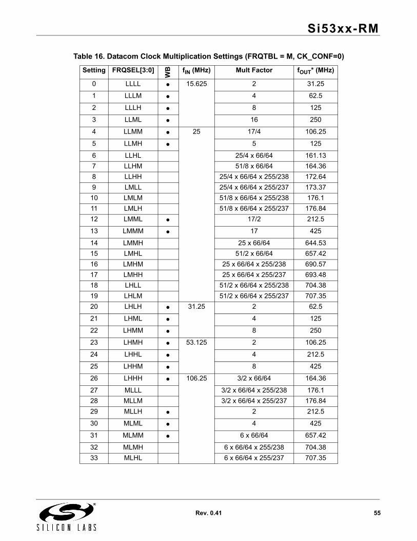
Si53xx-RM
Rev. 0.41 55
Table 16. Datacom Clock Multiplication Settings (FRQTBL = M, CK_CONF=0)
Setting FRQSEL[3:0]
WB fIN (MHz) Mult Factor fOUT* (MHz)
0 LLLL 15.625 2 31.25
1 LLLM 4 62.5
2 LLLH 8 125
3 LLML 16 250
4 LLMM 25 17/4 106.25
5 LLMH 5 125
6 LLHL 25/4 x 66/64 161.13
7 LLHM 51/8 x 66/64 164.36
8 LLHH 25/4 x 66/64 x 255/238 172.64
9 LMLL 25/4 x 66/64 x 255/237 173.37
10 LMLM 51/8 x 66/64 x 255/238 176.1
11 LMLH 51/8 x 66/64 x 255/237 176.84
12 LMML 17/2 212.5
13 LMMM 17 425
14 LMMH 25 x 66/64 644.53
15 LMHL 51/2 x 66/64 657.42
16 LMHM 25 x 66/64 x 255/238 690.57
17 LMHH 25 x 66/64 x 255/237 693.48
18 LHLL 51/2 x 66/64 x 255/238 704.38
19 LHLM 51/2 x 66/64 x 255/237 707.35
20 LHLH 31.25 2 62.5
21 LHML 4 125
22 LHMM 8 250
23 LHMH 53.125 2 106.25
24 LHHL 4 212.5
25 LHHM 8 425
26 LHHH 106.25 3/2 x 66/64 164.36
27 MLLL 3/2 x 66/64 x 255/238 176.1
28 MLLM 3/2 x 66/64 x 255/237 176.84
29 MLLH 2 212.5
30 MLML 4 425
31 MLMM 6 x 66/64 657.42
32 MLMH 6 x 66/64 x 255/238 704.38
33 MLHL 6 x 66/64 x 255/237 707.35
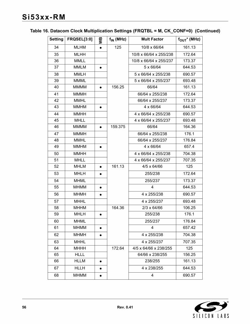
Si53xx-RM
56 Rev. 0.41
34 MLHM 125 10/8 x 66/64 161.13
35 MLHH 10/8 x 66/64 x 255/238 172.64
36 MMLL 10/8 x 66/64 x 255/237 173.37
37 MMLM 5 x 66/64 644.53
38 MMLH 5 x 66/64 x 255/238 690.57
39 MMML 5 x 66/64 x 255/237 693.48
40 MMMM 156.25 66/64 161.13
41 MMMH 66/64 x 255/238 172.64
42 MMHL 66/64 x 255/237 173.37
43 MMHM 4 x 66/64 644.53
44 MMHH 4 x 66/64 x 255/238 690.57
45 MHLL 4 x 66/64 x 255/237 693.48
46 MMMM 159.375 66/64 164.36
47 MMMH 66/64 x 255/238 176.1
48 MMHL 66/64 x 255/237 176.84
49 MMHM 4 x 66/64 657.4
50 MMHH 4 x 66/64 x 255/238 704.38
51 MHLL 4 x 66/64 x 255/237 707.35
52 MHLM 161.13 4/5 x 64/66 125
53 MHLH 255/238 172.64
54 MHML 255/237 173.37
55 MHMM 4 644.53
56 MHMH 4 x 255/238 690.57
57 MHHL 4 x 255/237 693.48
58 MHHM 164.36 2/3 x 64/66 106.25
59 MHLH 255/238 176.1
60 MHML 255/237 176.84
61 MHMM 4 657.42
62 MHMH 4 x 255/238 704.38
63 MHHL 4 x 255/237 707.35
64 MHHH 172.64 4/5 x 64/66 x 238/255 125
65 HLLL 64/66 x 238/255 156.25
66 HLLM 238/255 161.13
67 HLLH 4 x 238/255 644.53
68 MHMM 4 690.57
Table 16. Datacom Clock Multiplication Settings (FRQTBL = M, CK_CONF=0) (Continued)
Setting FRQSEL[3:0]
WB fIN (MHz) Mult Factor fOUT* (MHz)
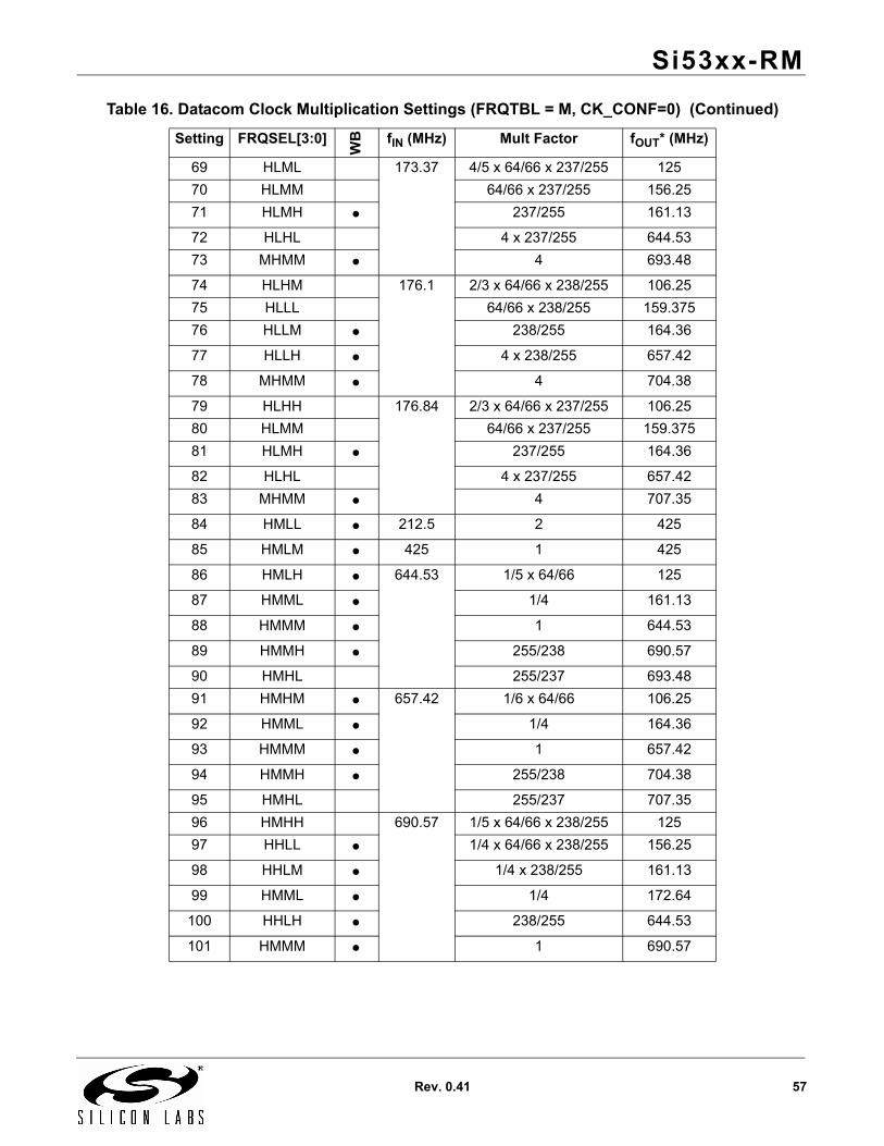
Si53xx-RM
Rev. 0.41 57
69 HLML 173.37 4/5 x 64/66 x 237/255 125
70 HLMM 64/66 x 237/255 156.25
71 HLMH 237/255 161.13
72 HLHL 4 x 237/255 644.53
73 MHMM 4 693.48
74 HLHM 176.1 2/3 x 64/66 x 238/255 106.25
75 HLLL 64/66 x 238/255 159.375
76 HLLM 238/255 164.36
77 HLLH 4 x 238/255 657.42
78 MHMM 4 704.38
79 HLHH 176.84 2/3 x 64/66 x 237/255 106.25
80 HLMM 64/66 x 237/255 159.375
81 HLMH 237/255 164.36
82 HLHL 4 x 237/255 657.42
83 MHMM 4 707.35
84 HMLL 212.5 2 425
85 HMLM 425 1 425
86 HMLH 644.53 1/5 x 64/66 125
87 HMML 1/4 161.13
88 HMMM 1 644.53
89 HMMH 255/238 690.57
90 HMHL 255/237 693.48
91 HMHM 657.42 1/6 x 64/66 106.25
92 HMML 1/4 164.36
93 HMMM 1 657.42
94 HMMH 255/238 704.38
95 HMHL 255/237 707.35
96 HMHH 690.57 1/5 x 64/66 x 238/255 125
97 HHLL 1/4 x 64/66 x 238/255 156.25
98 HHLM 1/4 x 238/255 161.13
99 HMML 1/4 172.64
100 HHLH 238/255 644.53
101 HMMM 1 690.57
Table 16. Datacom Clock Multiplication Settings (FRQTBL = M, CK_CONF=0) (Continued)
Setting FRQSEL[3:0]
WB fIN (MHz) Mult Factor fOUT* (MHz)
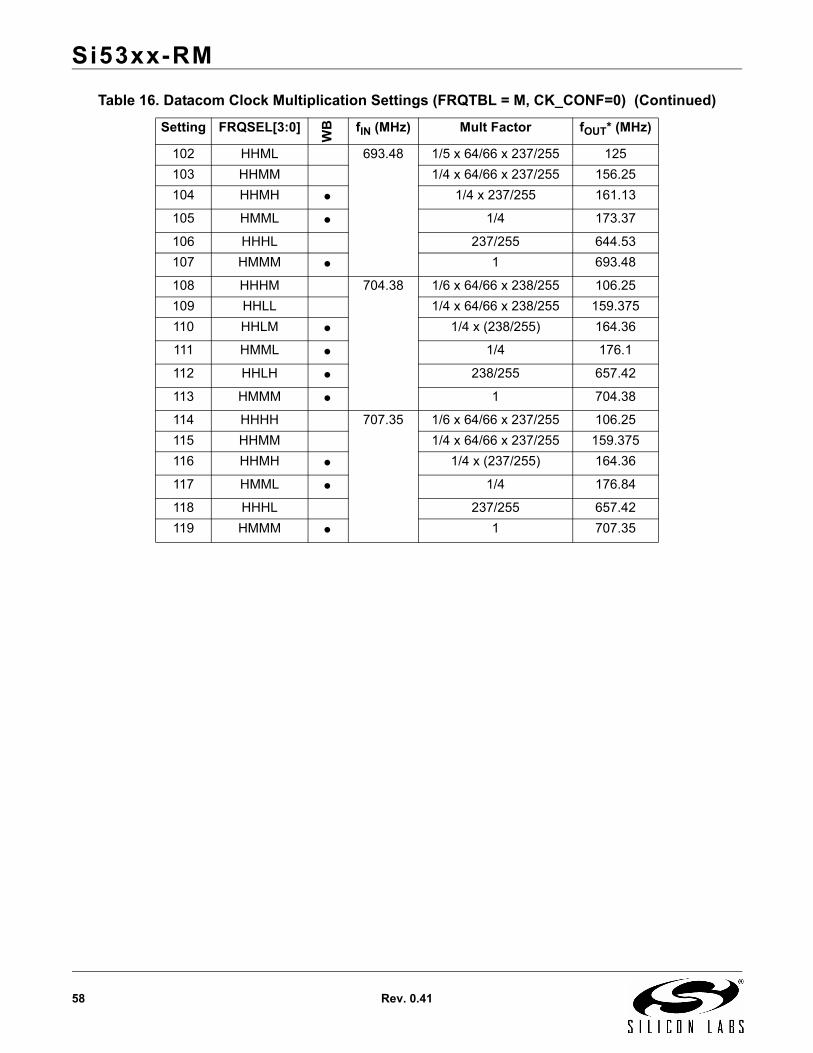
Si53xx-RM
58 Rev. 0.41
102 HHML 693.48 1/5 x 64/66 x 237/255 125
103 HHMM 1/4 x 64/66 x 237/255 156.25
104 HHMH 1/4 x 237/255 161.13
105 HMML 1/4 173.37
106 HHHL 237/255 644.53
107 HMMM 1 693.48
108 HHHM 704.38 1/6 x 64/66 x 238/255 106.25
109 HHLL 1/4 x 64/66 x 238/255 159.375
110 HHLM 1/4 x (238/255) 164.36
111 HMML 1/4 176.1
112 HHLH 238/255 657.42
113 HMMM 1 704.38
114 HHHH 707.35 1/6 x 64/66 x 237/255 106.25
115 HHMM 1/4 x 64/66 x 237/255 159.375
116 HHMH 1/4 x (237/255) 164.36
117 HMML 1/4 176.84
118 HHHL 237/255 657.42
119 HMMM 1 707.35
Table 16. Datacom Clock Multiplication Settings (FRQTBL = M, CK_CONF=0) (Continued)
Setting FRQSEL[3:0]
WB fIN (MHz) Mult Factor fOUT* (MHz)
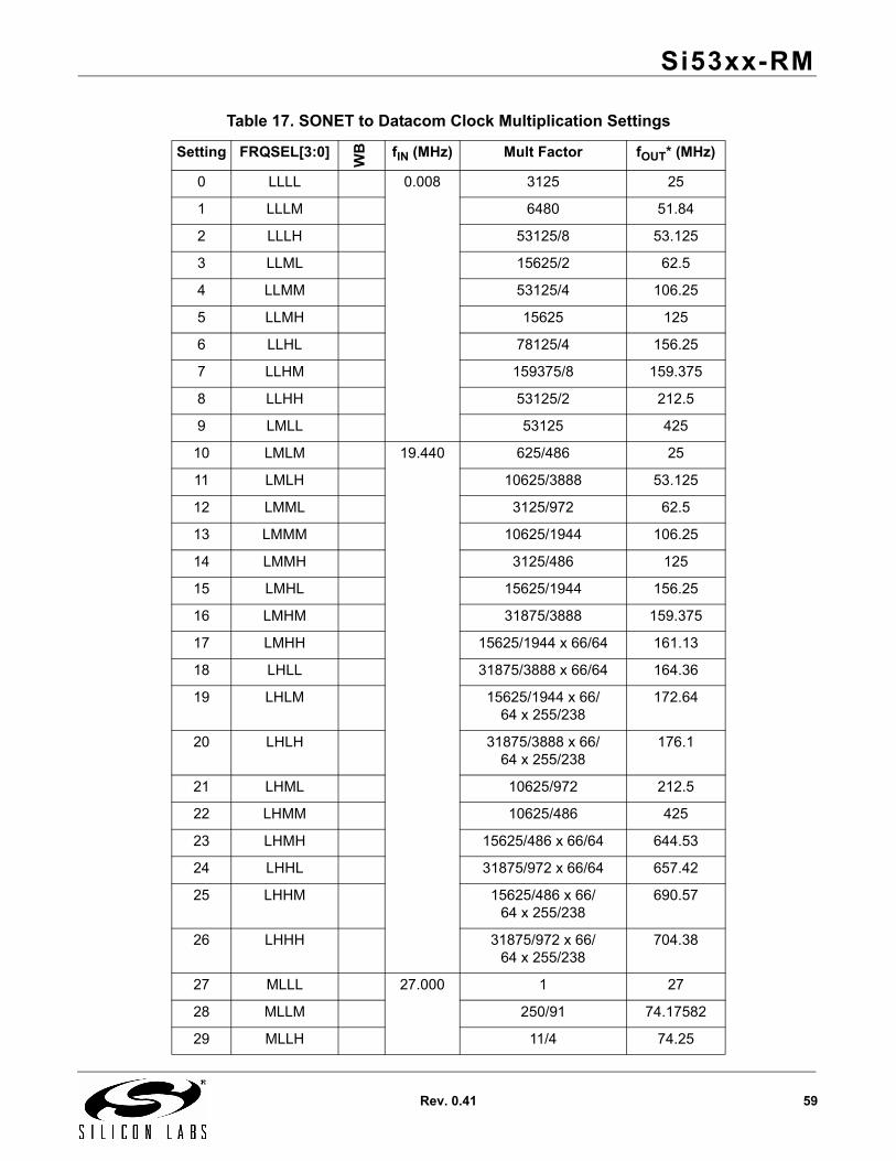
Si53xx-RM
Rev. 0.41 59
Table 17. SONET to Datacom Clock Multiplication Settings
Setting FRQSEL[3:0]
WB fIN (MHz) Mult Factor fOUT* (MHz)
0 LLLL 0.008 3125 25
1 LLLM 6480 51.84
2 LLLH 53125/8 53.125
3 LLML 15625/2 62.5
4 LLMM 53125/4 106.25
5 LLMH 15625 125
6 LLHL 78125/4 156.25
7 LLHM 159375/8 159.375
8 LLHH 53125/2 212.5
9 LMLL 53125 425
10 LMLM 19.440 625/486 25
11 LMLH 10625/3888 53.125
12 LMML 3125/972 62.5
13 LMMM 10625/1944 106.25
14 LMMH 3125/486 125
15 LMHL 15625/1944 156.25
16 LMHM 31875/3888 159.375
17 LMHH 15625/1944 x 66/64 161.13
18 LHLL 31875/3888 x 66/64 164.36
19 LHLM 15625/1944 x 66/64 x 255/238
172.64
20 LHLH 31875/3888 x 66/64 x 255/238
176.1
21 LHML 10625/972 212.5
22 LHMM 10625/486 425
23 LHMH 15625/486 x 66/64 644.53
24 LHHL 31875/972 x 66/64 657.42
25 LHHM 15625/486 x 66/64 x 255/238
690.57
26 LHHH 31875/972 x 66/64 x 255/238
704.38
27 MLLL 27.000 1 27
28 MLLM 250/91 74.17582
29 MLLH 11/4 74.25
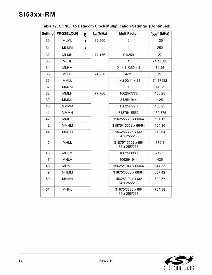
Si53xx-RM
60 Rev. 0.41
30 MLML 62.500 2 125
31 MLMM 4 250
32 MLMH 74.176 91/250 27
33 MLHL 1 74.17582
34 MLHM 91 x 11/250 x 4 74.25
35 MLHH 74.250 4/11 27
36 MMLL 4 x 250/11 x 91 74.17582
37 MMLM 1 74.25
38 MMLH 77.760 10625/7776 106.25
39 MMML 3125/1944 125
40 MMMM 15625/7776 156.25
41 MMMH 31875/15552 159.375
42 MMHL 15625/7776 x 66/64 161.13
43 MMHM 31875/15552 x 66/64 164.36
44 MMHH 15625/7776 x 66/64 x 255/238
172.64
45 MHLL 31875/15552 x 66/64 x 255/238
176.1
46 MHLM 10625/3888 212.5
47 MHLH 10625/1944 425
48 MHML 15625/1944 x 66/64 644.53
49 MHMM 31875/3888 x 66/64 657.42
50 MHMH 15625/1944 x 66/64 x 255/238
690.57
51 MHHL 31875/3888 x 66/64 x 255/238
704.38
Table 17. SONET to Datacom Clock Multiplication Settings (Continued)
Setting FRQSEL[3:0]
WB fIN (MHz) Mult Factor fOUT* (MHz)
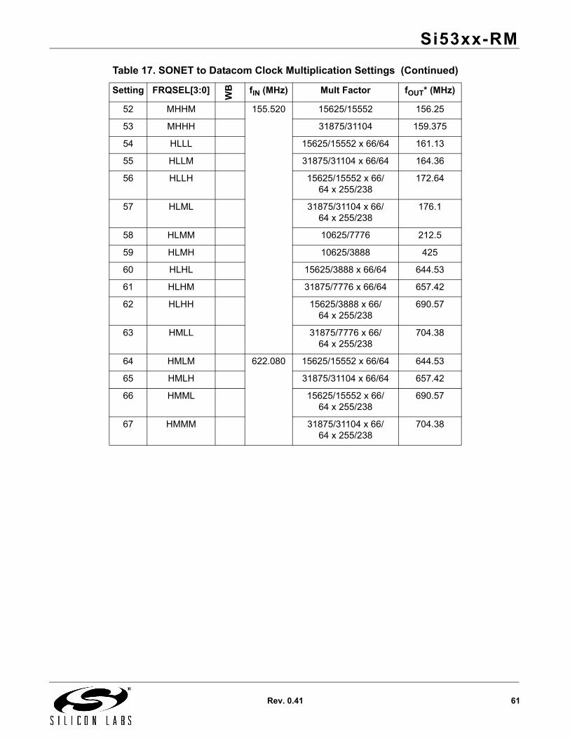
Si53xx-RM
Rev. 0.41 61
52 MHHM 155.520 15625/15552 156.25
53 MHHH 31875/31104 159.375
54 HLLL 15625/15552 x 66/64 161.13
55 HLLM 31875/31104 x 66/64 164.36
56 HLLH 15625/15552 x 66/64 x 255/238
172.64
57 HLML 31875/31104 x 66/64 x 255/238
176.1
58 HLMM 10625/7776 212.5
59 HLMH 10625/3888 425
60 HLHL 15625/3888 x 66/64 644.53
61 HLHM 31875/7776 x 66/64 657.42
62 HLHH 15625/3888 x 66/64 x 255/238
690.57
63 HMLL 31875/7776 x 66/64 x 255/238
704.38
64 HMLM 622.080 15625/15552 x 66/64 644.53
65 HMLH 31875/31104 x 66/64 657.42
66 HMML 15625/15552 x 66/64 x 255/238
690.57
67 HMMM 31875/31104 x 66/64 x 255/238
704.38
Table 17. SONET to Datacom Clock Multiplication Settings (Continued)
Setting FRQSEL[3:0]
WB fIN (MHz) Mult Factor fOUT* (MHz)
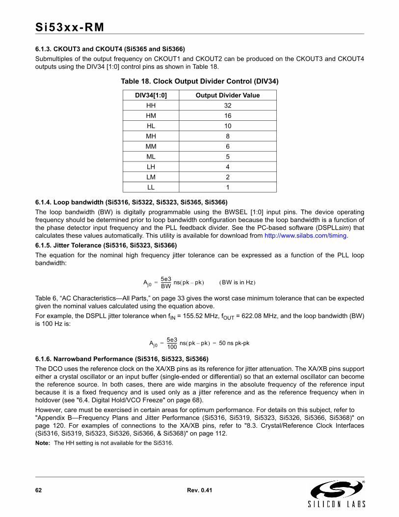
Si53xx-RM
62 Rev. 0.41
6.1.3. CKOUT3 and CKOUT4 (Si5365 and Si5366)
Submultiples of the output frequency on CKOUT1 and CKOUT2 can be produced on the CKOUT3 and CKOUT4outputs using the DIV34 [1:0] control pins as shown in Table 18.
6.1.4. Loop bandwidth (Si5316, Si5322, Si5323, Si5365, Si5366)
The loop bandwidth (BW) is digitally programmable using the BWSEL [1:0] input pins. The device operatingfrequency should be determined prior to loop bandwidth configuration because the loop bandwidth is a function ofthe phase detector input frequency and the PLL feedback divider. See the PC-based software (DSPLLsim) thatcalculates these values automatically. This utility is available for download from http://www.silabs.com/timing.
6.1.5. Jitter Tolerance (Si5316, Si5323, Si5366)
The equation for the nominal high frequency jitter tolerance can be expressed as a function of the PLL loopbandwidth:
Table 6, “AC Characteristics—All Parts,” on page 33 gives the worst case minimum tolerance that can be expectedgiven the nominal values calculated using the equation above.
For example, the DSPLL jitter tolerance when fIN = 155.52 MHz, fOUT = 622.08 MHz, and the loop bandwidth (BW)is 100 Hz is:
6.1.6. Narrowband Performance (Si5316, Si5323, Si5366)
The DCO uses the reference clock on the XA/XB pins as its reference for jitter attenuation. The XA/XB pins supporteither a crystal oscillator or an input buffer (single-ended or differential) so that an external oscillator can becomethe reference source. In both cases, there are wide margins in the absolute frequency of the reference inputbecause it is a fixed frequency and is used only as a jitter reference and as the reference frequency when inholdover (see "6.4. Digital Hold/VCO Freeze" on page 68).
However, care must be exercised in certain areas for optimum performance. For details on this subject, refer to"Appendix B—Frequency Plans and Jitter Performance (Si5316, Si5319, Si5323, Si5326, Si5366, Si5368)" onpage 120. For examples of connections to the XA/XB pins, refer to "8.3. Crystal/Reference Clock Interfaces(Si5316, Si5319, Si5323, Si5326, Si5366, & Si5368)" on page 112.
Note: The HH setting is not available for the Si5316.
Table 18. Clock Output Divider Control (DIV34)
DIV34[1:0] Output Divider Value
HH 32
HM 16
HL 10
MH 8
MM 6
ML 5
LH 4
LM 2
LL 1
Aj05e3BW---------- ns pk pk– BW is in Hz =
Aj05e3100---------- ns pk pk– 50 ns pk-pk= =
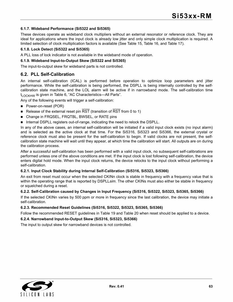
Si53xx-RM
Rev. 0.41 63
6.1.7. Wideband Performance (Si5322 and Si5365)
These devices operate as wideband clock multipliers without an external resonator or reference clock. They areideal for applications where the input clock is already low jitter and only simple clock multiplication is required. Alimited selection of clock multiplication factors is available (See Table 15, Table 16, and Table 17).
6.1.8. Lock Detect (Si5322 and Si5365)
A PLL loss of lock indicator is not available in the wideband mode of operation.
6.1.9. Wideband Input-to-Output Skew (Si5322 and Si5365)
The input-to-output skew for wideband parts is not controlled.
6.2. PLL Self-CalibrationAn internal self-calibration (ICAL) is performed before operation to optimize loop parameters and jitterperformance. While the self-calibration is being performed, the DSPLL is being internally controlled by the self-calibration state machine, and the LOL alarm will be active if in narrowband mode. The self-calibration timetLOCKHW is given in Table 6, “AC Characteristics—All Parts”.
Any of the following events will trigger a self-calibration:
Power-on-reset (POR)
Release of the external reset pin RST (transition of RST from 0 to 1)
Change in FRQSEL, FRQTBL, BWSEL, or RATE pins
Internal DSPLL registers out-of-range, indicating the need to relock the DSPLL.
In any of the above cases, an internal self-calibration will be initiated if a valid input clock exists (no input alarm)and is selected as the active clock at that time. For the Si5316, Si5323 and Si5366, the external crystal orreference clock must also be present for the self-calibration to begin. If valid clocks are not present, the self-calibration state machine will wait until they appear, at which time the calibration will start. All outputs are on duringthe calibration process.
After a successful self-calibration has been performed with a valid input clock, no subsequent self-calibrations areperformed unless one of the above conditions are met. If the input clock is lost following self-calibration, the deviceenters digital hold mode. When the input clock returns, the device relocks to the input clock without performing aself-calibration.
6.2.1. Input Clock Stability during Internal Self-Calibration (Si5316, Si5323, Si5366)
An exit from reset must occur when the selected CKINn clock is stable in frequency with a frequency value that iswithin the operating range that is reported by DSPLLsim. The other CKINs must also either be stable in frequencyor squelched during a reset.
6.2.2. Self-Calibration caused by Changes in Input Frequency (Si5316, Si5322, Si5323, Si5365, Si5366)
If the selected CKINn varies by 500 ppm or more in frequency since the last calibration, the device may initiate aself-calibration.
6.2.3. Recommended Reset Guidelines (Si5316, Si5322, Si5323, Si5365, Si5366)
Follow the recommended RESET guidelines in Table 19 and Table 20 when reset should be applied to a device.
6.2.4. Narrowband Input-to-Output Skew (Si5316, Si5323, Si5366)
The input to output skew for narrowband devices is not controlled.
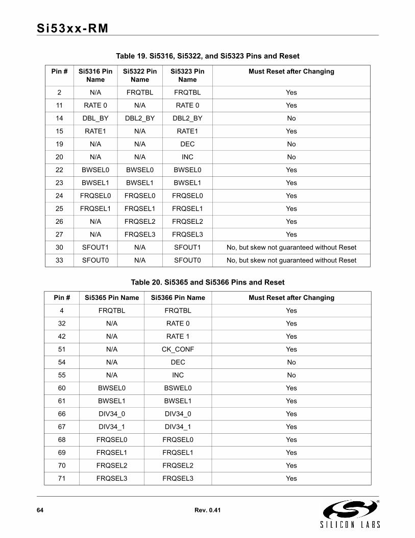
Si53xx-RM
64 Rev. 0.41
Table 19. Si5316, Si5322, and Si5323 Pins and Reset
Pin # Si5316 Pin Name
Si5322 Pin Name
Si5323 Pin Name
Must Reset after Changing
2 N/A FRQTBL FRQTBL Yes
11 RATE 0 N/A RATE 0 Yes
14 DBL_BY DBL2_BY DBL2_BY No
15 RATE1 N/A RATE1 Yes
19 N/A N/A DEC No
20 N/A N/A INC No
22 BWSEL0 BWSEL0 BWSEL0 Yes
23 BWSEL1 BWSEL1 BWSEL1 Yes
24 FRQSEL0 FRQSEL0 FRQSEL0 Yes
25 FRQSEL1 FRQSEL1 FRQSEL1 Yes
26 N/A FRQSEL2 FRQSEL2 Yes
27 N/A FRQSEL3 FRQSEL3 Yes
30 SFOUT1 N/A SFOUT1 No, but skew not guaranteed without Reset
33 SFOUT0 N/A SFOUT0 No, but skew not guaranteed without Reset
Table 20. Si5365 and Si5366 Pins and Reset
Pin # Si5365 Pin Name Si5366 Pin Name Must Reset after Changing
4 FRQTBL FRQTBL Yes
32 N/A RATE 0 Yes
42 N/A RATE 1 Yes
51 N/A CK_CONF Yes
54 N/A DEC No
55 N/A INC No
60 BWSEL0 BSWEL0 Yes
61 BWSEL1 BWSEL1 Yes
66 DIV34_0 DIV34_0 Yes
67 DIV34_1 DIV34_1 Yes
68 FRQSEL0 FRQSEL0 Yes
69 FRQSEL1 FRQSEL1 Yes
70 FRQSEL2 FRQSEL2 Yes
71 FRQSEL3 FRQSEL3 Yes
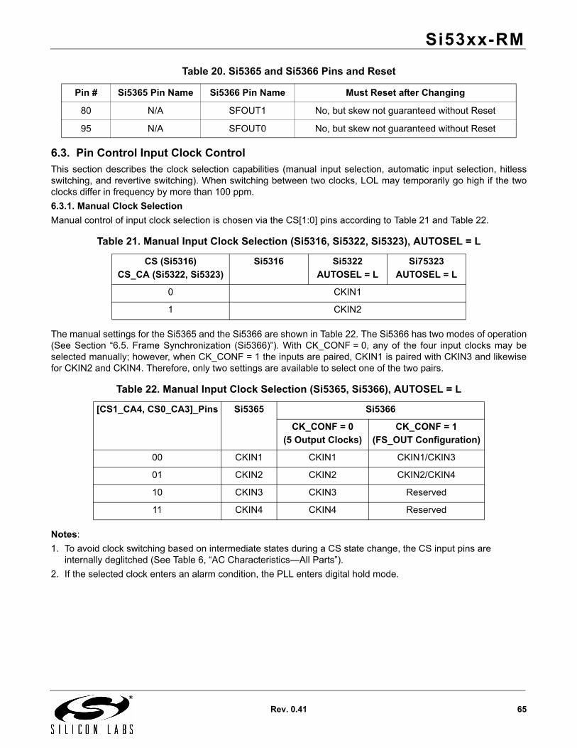
Si53xx-RM
Rev. 0.41 65
6.3. Pin Control Input Clock ControlThis section describes the clock selection capabilities (manual input selection, automatic input selection, hitlessswitching, and revertive switching). When switching between two clocks, LOL may temporarily go high if the twoclocks differ in frequency by more than 100 ppm.
6.3.1. Manual Clock Selection
Manual control of input clock selection is chosen via the CS[1:0] pins according to Table 21 and Table 22.
The manual settings for the Si5365 and the Si5366 are shown in Table 22. The Si5366 has two modes of operation(See Section “6.5. Frame Synchronization (Si5366)”). With CK_CONF = 0, any of the four input clocks may beselected manually; however, when CK_CONF = 1 the inputs are paired, CKIN1 is paired with CKIN3 and likewisefor CKIN2 and CKIN4. Therefore, only two settings are available to select one of the two pairs.
Notes:
1. To avoid clock switching based on intermediate states during a CS state change, the CS input pins are internally deglitched (See Table 6, “AC Characteristics—All Parts”).
2. If the selected clock enters an alarm condition, the PLL enters digital hold mode.
80 N/A SFOUT1 No, but skew not guaranteed without Reset
95 N/A SFOUT0 No, but skew not guaranteed without Reset
Table 21. Manual Input Clock Selection (Si5316, Si5322, Si5323), AUTOSEL = L
CS (Si5316)
CS_CA (Si5322, Si5323)
Si5316 Si5322
AUTOSEL = L
Si75323
AUTOSEL = L
0 CKIN1
1 CKIN2
Table 22. Manual Input Clock Selection (Si5365, Si5366), AUTOSEL = L
[CS1_CA4, CS0_CA3]_Pins Si5365 Si5366
CK_CONF = 0
(5 Output Clocks)
CK_CONF = 1
(FS_OUT Configuration)
00 CKIN1 CKIN1 CKIN1/CKIN3
01 CKIN2 CKIN2 CKIN2/CKIN4
10 CKIN3 CKIN3 Reserved
11 CKIN4 CKIN4 Reserved
Table 20. Si5365 and Si5366 Pins and Reset
Pin # Si5365 Pin Name Si5366 Pin Name Must Reset after Changing
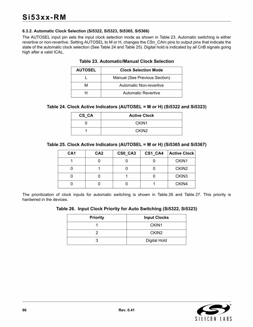
Si53xx-RM
66 Rev. 0.41
6.3.2. Automatic Clock Selection (Si5322, Si5323, Si5365, Si5366)
The AUTOSEL input pin sets the input clock selection mode as shown in Table 23. Automatic switching is eitherrevertive or non-revertive. Setting AUTOSEL to M or H, changes the CSn_CAm pins to output pins that indicate thestate of the automatic clock selection (See Table 24 and Table 25). Digital hold is indicated by all CnB signals goinghigh after a valid ICAL.
The prioritization of clock inputs for automatic switching is shown in Table 26 and Table 27. This priority ishardwired in the devices.
Table 23. Automatic/Manual Clock Selection
AUTOSEL Clock Selection Mode
L Manual (See Previous Section)
M Automatic Non-revertive
H Automatic Revertive
Table 24. Clock Active Indicators (AUTOSEL = M or H) (Si5322 and Si5323)
CS_CA Active Clock
0 CKIN1
1 CKIN2
Table 25. Clock Active Indicators (AUTOSEL = M or H) (Si5365 and Si5367)
CA1 CA2 CS0_CA3 CS1_CA4 Active Clock
1 0 0 0 CKIN1
0 1 0 0 CKIN2
0 0 1 0 CKIN3
0 0 0 1 CKIN4
Table 26. Input Clock Priority for Auto Switching (Si5322, Si5323)
Priority Input Clocks
1 CKIN1
2 CKIN2
3 Digital Hold
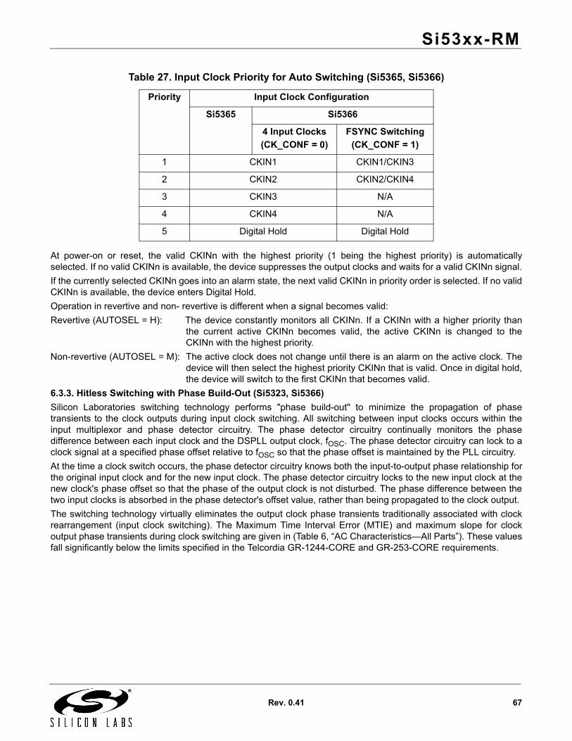
Si53xx-RM
Rev. 0.41 67
At power-on or reset, the valid CKINn with the highest priority (1 being the highest priority) is automaticallyselected. If no valid CKINn is available, the device suppresses the output clocks and waits for a valid CKINn signal.
If the currently selected CKINn goes into an alarm state, the next valid CKINn in priority order is selected. If no validCKINn is available, the device enters Digital Hold.
Operation in revertive and non- revertive is different when a signal becomes valid:
Revertive (AUTOSEL = H): The device constantly monitors all CKINn. If a CKINn with a higher priority thanthe current active CKINn becomes valid, the active CKINn is changed to theCKINn with the highest priority.
Non-revertive (AUTOSEL = M): The active clock does not change until there is an alarm on the active clock. Thedevice will then select the highest priority CKINn that is valid. Once in digital hold,the device will switch to the first CKINn that becomes valid.
6.3.3. Hitless Switching with Phase Build-Out (Si5323, Si5366)
Silicon Laboratories switching technology performs "phase build-out" to minimize the propagation of phasetransients to the clock outputs during input clock switching. All switching between input clocks occurs within theinput multiplexor and phase detector circuitry. The phase detector circuitry continually monitors the phasedifference between each input clock and the DSPLL output clock, fOSC. The phase detector circuitry can lock to aclock signal at a specified phase offset relative to fOSC so that the phase offset is maintained by the PLL circuitry.
At the time a clock switch occurs, the phase detector circuitry knows both the input-to-output phase relationship forthe original input clock and for the new input clock. The phase detector circuitry locks to the new input clock at thenew clock's phase offset so that the phase of the output clock is not disturbed. The phase difference between thetwo input clocks is absorbed in the phase detector's offset value, rather than being propagated to the clock output.
The switching technology virtually eliminates the output clock phase transients traditionally associated with clockrearrangement (input clock switching). The Maximum Time Interval Error (MTIE) and maximum slope for clockoutput phase transients during clock switching are given in (Table 6, “AC Characteristics—All Parts”). These valuesfall significantly below the limits specified in the Telcordia GR-1244-CORE and GR-253-CORE requirements.
Table 27. Input Clock Priority for Auto Switching (Si5365, Si5366)
Priority Input Clock Configuration
Si5365 Si5366
4 Input Clocks
(CK_CONF = 0)
FSYNC Switching
(CK_CONF = 1)
1 CKIN1 CKIN1/CKIN3
2 CKIN2 CKIN2/CKIN4
3 CKIN3 N/A
4 CKIN4 N/A
5 Digital Hold Digital Hold
Si53xx-RM
68 Rev. 0.41
6.4. Digital Hold/VCO FreezeAll Any-Rate Precision Clock devices feature a hold over or VCO freeze mode, whereby the DSPLL is locked to adigital value.
6.4.1. Narrowband Digital Hold (Si5316, Si5323, Si5366)
If an LOS or FOS condition exists on the selected input clock, the device enters digital hold. In this mode, thedevice provides a stable output frequency until the input clock returns and is validated. When the device entersdigital hold, the internal oscillator is initially held to its last frequency value. Next, the internal oscillator slowlytransitions to a historical average frequency value that was taken over a time window of 6,711 ms in size thatended 26 ms before the device entered digital hold. This frequency value is taken from an internal memory locationthat keeps a record of previous DSPLL frequency values. By using a historical average frequency, input clockphase and frequency transients that may occur immediately preceding loss of clock or any event causing digitalhold do not affect the digital hold frequency. Also, noise related to input clock jitter or internal PLL jitter isminimized.
If a highly stable reference, such as an oven-controlled crystal oscillator, is supplied at XA/XB, an extremely stabledigital hold can be achieved. If a crystal is supplied at the XA/XB port, the digital hold stability will be limited by thestability of the crystal; Table 6, “AC Characteristics—All Parts” gives the specifications related to the digital holdfunction.
6.4.2. Recovery from Digital Hold (Si5316, Si5323, Si5366)
When the input clock signal returns, the device transitions from digital hold to the selected input clock. The deviceperforms hitless recovery from digital hold. The clock transition from digital hold to the returned input clock includes"phase buildout" to absorb the phase difference between the digital hold clock phase and the input clock phase.See Table 6, “AC Characteristics—All Parts” for specifications.
6.4.3. Wideband VCO Freeze (Si5322, Si5365)
If an LOS condition exists on the selected input clock, the device freezes the VCO. In this mode, the deviceprovides a stable output frequency until the input clock returns and is validated. When the device enters VCOfreeze, the internal oscillator is initially held to its last frequency value.
6.5. Frame Synchronization (Si5366)FSYNC is used in applications that require a synchronizing pulse that has an exact number of periods of a high-rate clock, Frame Synchronization is selected by setting CK_CONF = 1 and FRQTBL = L). In a typical framesynchronization application, CKIN1 and CKIN2 are high-speed input clocks from primary and secondary clockgeneration cards and CKIN3 and CKIN4 are their associated primary and secondary frame synchronizationsignals. The device generates four output clocks and a frame sync output FS_OUT. CKIN3 and CKIN4 control thephase of FS_OUT.
The frame sync inputs supplied to CKIN3 and CKIN4 must be 8 kHz. Since the frequency of FS_OUT is derivedfrom CKOUT2, CKOUT2 must be a standard SONET frequency (e.g. 19.44 MHz, 77.76 MHz). Table 15 lists theinput frequency/clock multiplication ratio combinations supporting an 8 kHz output on FS_OUT.
Si53xx-RM
Rev. 0.41 69
6.6. Output Phase Adjust (Si5323, Si5366)Overall device skew (CKINn to CKOUT_n phase delay) is controllable via the INC and DEC input pins. A positivepulse applied at the INC pin increases the device skew by 1/fOSC, one period of the DCO output clock. A pulse onthe DEC pin decreases the skew by the same amount. Since fOSC is close to 5 GHz, the resolution of the skewcontrol is approximately 200 ps. Using the INC and DEC pins, there is no limit to the range of skew adjustment thatcan be made. Following a power-up or reset, the skew will revert to the reset value. See Table 6, “ACCharacteristics—All Parts” for specifications related to the phase adjust feature.
The INC pin function is not available for all frequency table selections. DSPLLsim reports this whenever it is usedto implement a frequency plan.
6.6.1. FSYNC Realignment (Si5366)
The FS_ALIGN pin controls the realignment of FS_OUT to the active CKIN3 or CKIN4 input. The currently activeframe sync input is determined by which input clock is currently being used by the PLL. For example, if CKIN1 isbeing selected as the PLL input, CKIN3 is the currently-active frame sync input. If neither CKIN3 or CKIN4 arecurrently active (digital hold), the realignment request is ignored. The active edge used for realignment is theCKIN3 or CKIN4 rising edge.
FS_ALIGN operates in Level Sensitive mode (See Figure 13, “Frame Synchronization Timing in Level SensitiveMode,”). While FS_ALIGN is active, each active edge of the currently-active frame sync input (CKIN3 or CKIN4) isused to control the NC5 output divider and therefore the FS_OUT phase. Note that while the realignment control isactive, it cannot be guaranteed that a fixed number of high-frequency clock (CKOUT2) cycles exists between eachFS_OUT cycle.
The resolution of the phase realignment is 1 clock cycle of CKOUT2. If the realignment control is not active, theNC5 divider will continuously divide down its fCKOUT2 input. This guarantees a fixed number of high-frequencyclock (CKOUT2) cycles between each FS_OUT cycle.
At power-up or any time after the PLL has lost lock and relocked, the device automatically performs a realignmentof FS_OUT using the currently active sync input. After this, as long as the PLL remains in lock and a realignment isnot requested, FS_OUT will include a fixed number of high-speed clock cycles, even if input clock switches areperformed. If many clock switches are performed in phase build-out mode, it is possible that the input sync tooutput sync phase relationship will shift due to the accumulated residual phase transients of the phase build-outcircuitry. If the sync alignment error exceeds the threshold in either the positive or negative direction, an alignmentalarm becomes active. If it is then desired to reestablish the desired input-to-output sync phase relationship, arealignment can be performed. A realignment request may cause FS_OUT to instantaneously shift its output edgelocation in order to align with the active input sync phase.
6.6.2. Including FSYNC Inputs in Clock Selection (Si5366)
The frame sync inputs, CKIN3 and CKIN4, are both monitored for loss-of-signal (LOS3_INT and LOS4_INT)conditions. To include these LOS alarms in the input clock selection algorithm, set FSYNC_SWTCH = 1. TheLOS3_INT is logically ORed with LOS1_INT and LOS4_INT is ORed with LOS2_INT as inputs to the clockselection state machine. If it is desired not to include these alarms in the clock selection algorithm, setFSYNC_SWTCH = 0. The frequency offset (FOS) alarms for CKIN1 and CKIN2 can also be included in the statemachine decision making as described in Section “6.9. Alarms”; however, in frame sync mode (CK_CONF = 1), theFOS alarms for CKIN3 and CKIN4 are ignored. See Table 32 on page 72.
6.6.3. FS_OUT Polarity and Pulse Width Control (Si5366)
Additional output controls are available for FS_OUT. FS_OUT is active high, and the pulse width is equal to oneperiod of the CKOUT2 output clock. For example, if CKOUT2 is 622.08 MHz, the FS_OUT pulse width will be 1/622.08e6 = 1.61 ns.
6.6.4. Using FS_OUT as a Fifth Output Clock (Si5366)
In applications where the frame synchronization functionality is not needed, FS_OUT can be used as a fifth clockoutput. In this case, no realignment requests should be made to the NC5 divider. (This is done by holdingFS_ALIGN to 0.)
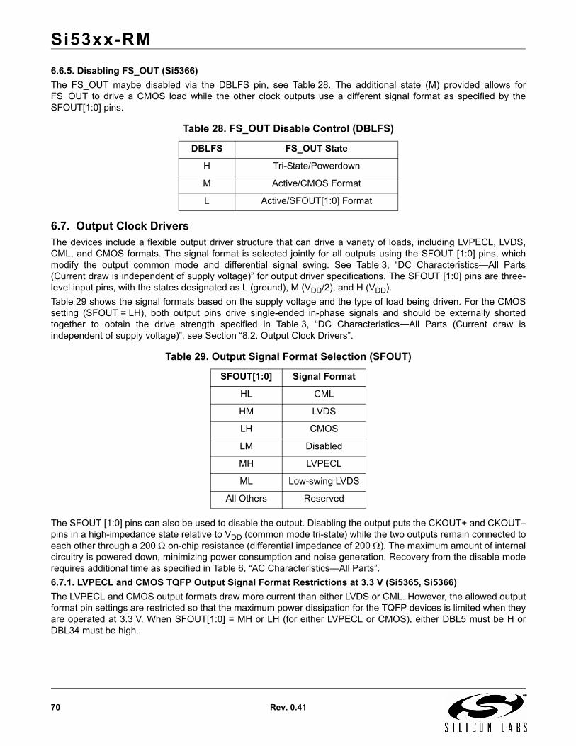
Si53xx-RM
70 Rev. 0.41
6.6.5. Disabling FS_OUT (Si5366)
The FS_OUT maybe disabled via the DBLFS pin, see Table 28. The additional state (M) provided allows forFS_OUT to drive a CMOS load while the other clock outputs use a different signal format as specified by theSFOUT[1:0] pins.
6.7. Output Clock DriversThe devices include a flexible output driver structure that can drive a variety of loads, including LVPECL, LVDS,CML, and CMOS formats. The signal format is selected jointly for all outputs using the SFOUT [1:0] pins, whichmodify the output common mode and differential signal swing. See Table 3, “DC Characteristics—All Parts(Current draw is independent of supply voltage)” for output driver specifications. The SFOUT [1:0] pins are three-level input pins, with the states designated as L (ground), M (VDD/2), and H (VDD).
Table 29 shows the signal formats based on the supply voltage and the type of load being driven. For the CMOSsetting (SFOUT = LH), both output pins drive single-ended in-phase signals and should be externally shortedtogether to obtain the drive strength specified in Table 3, “DC Characteristics—All Parts (Current draw isindependent of supply voltage)”, see Section “8.2. Output Clock Drivers”.
The SFOUT [1:0] pins can also be used to disable the output. Disabling the output puts the CKOUT+ and CKOUT–pins in a high-impedance state relative to VDD (common mode tri-state) while the two outputs remain connected toeach other through a 200 on-chip resistance (differential impedance of 200 ). The maximum amount of internalcircuitry is powered down, minimizing power consumption and noise generation. Recovery from the disable moderequires additional time as specified in Table 6, “AC Characteristics—All Parts”.
6.7.1. LVPECL and CMOS TQFP Output Signal Format Restrictions at 3.3 V (Si5365, Si5366)
The LVPECL and CMOS output formats draw more current than either LVDS or CML. However, the allowed outputformat pin settings are restricted so that the maximum power dissipation for the TQFP devices is limited when theyare operated at 3.3 V. When SFOUT[1:0] = MH or LH (for either LVPECL or CMOS), either DBL5 must be H orDBL34 must be high.
Table 28. FS_OUT Disable Control (DBLFS)
DBLFS FS_OUT State
H Tri-State/Powerdown
M Active/CMOS Format
L Active/SFOUT[1:0] Format
Table 29. Output Signal Format Selection (SFOUT)
SFOUT[1:0] Signal Format
HL CML
HM LVDS
LH CMOS
LM Disabled
MH LVPECL
ML Low-swing LVDS
All Others Reserved
Si53xx-RM
Rev. 0.41 71
6.8. PLL Bypass ModeThe Device supports a PLL Bypass Mode in which the selected input clock is fed directly to all enabled outputbuffers, bypassing the DSPLL. In PLL Bypass Mode, the input and output clocks will be at the same frequency. PLLBypass Mode is useful in a laboratory environment to measure system performance with and without the jitterattenuation provided by the DSPLL.
The DSBL2/BYPASS pin is used to select the PLL Bypass Mode according to Table 30.
Internally, the bypass path is implemented with high-speed differential signaling for low jitter.
6.9. AlarmsSummary alarms are available to indicate the overall status of the input signals and frame alignment (Si5366 only).Alarm outputs stay high until all the alarm conditions for that alarm output are cleared.
6.9.1. Loss-of-Signal Alarms (Si5316, Si5322, Si5323, Si5365, Si5366)
The device has loss-of-signal circuitry that continuously monitors CKINn for missing pulses. The LOS circuitrygenerates an internal LOSn_INT output signal that is processed with other alarms to generate CnB.
An LOS condition on CKIN1 causes the internal LOS1_INT alarm to become active. Similarly, an LOS condition onCKINn causes the LOSn_INT alarm to become active. Once a LOSn_INT alarm is asserted on one of the inputclocks, it remains asserted until that input clock is validated over a designated time period. The time to clearLOSn_INT after a valid input clock appears is listed in Table 6, “AC Characteristics—All Parts”. If another errorcondition on the same input clock is detected during the validation time then the alarm remains asserted and thevalidation time starts over.
6.9.1.1. Narrowband LOS Algorithm (Si5316, Si5323, Si5366)
The LOS circuitry divides down each input clock to produce an 8 kHz to 2 MHz signal. (For the Si5316, the outputof divider N3 (See Figure 1) is used.) The LOS circuitry over samples this divided down input clock using a 40 MHzclock to search for extended periods of time without input clock transitions. If the LOS monitor detects twice thenormal number of samples without a clock edge, a LOSn_INT alarm is declared. Table 6, “AC Characteristics—AllParts” gives the minimum and maximum amount of time for the LOS monitor to trigger.
To facilitate automatic hitless switching, the LOS triggering time is significantly reduced while in narrowband mode.
6.9.1.2. Wideband LOS Algorithm (Si5322, Si5365)
Each input clock is divided down to produce a 78 kHz to 1.2 MHz signal before entering the LOS monitoringcircuitry. The same LOS algorithm as described in the above section is then used.
6.9.2. FOS Alarms (Si5365 and Si5366)
If FOS Alarms are enabled (See Table 31), the internal frequency offset alarms (FOSn_INT) indicate if the inputclocks are within a specified frequency band relative to the frequency of CKIN2. The frequency offset monitoringcircuitry compares the frequency of the input clock(s) with CKIN2. If the frequency offset of an input clock exceedsa preset frequency offset threshold, an FOS alarm (FOSn_INT) is declared for that clock input. Note that FOSmonitoring is not available on CKIN3 and CKIN4 if CK_CONF = 1. The device supports FOS hysteresis per GR-1244-CORE, making the device less susceptible to FOS alarm chattering. A TCXO or OCXO reference clock mustbe used in conjunction with either the SMC or Stratum 3/3E settings. Note that the wander can cause false FOSalarms.
Table 30. DSBL2/BYPASS Pin Settings
DSBL2/BYPASS Function
L CKOUT2 Enabled
M CKOUT2 Disabled
H PLL Bypass Mode w/ CKOUT2 Enabled
Si53xx-RM
72 Rev. 0.41
6.9.3. FSYNC Align Alarm (Si5366 and CK_CONF = 1 and FRQTBL = L)
At power-up or any time after the PLL has lost lock and relocked, the device automatically performs a realignmentof FS_OUT using the currently active sync input. After this, as long as the PLL remains in lock and a realignment isnot requested, FS_OUT will include a fixed number of high-speed clock cycles, even if input clock switches areperformed. If many clock switches are performed in phase build-out mode, it is possible that the input sync tooutput sync phase relationship will shift due to the accumulated residual phase transients of the phase build-outcircuitry. The internal ALIGN_INT signal is asserted when the accumulated phase errors exceeds two cycles ofCKOUT2.
6.9.4. C1B and C2B Alarm Outputs (Si5316, Si5322, Si5323)
The alarm outputs (C1B and C2B) are determined directly by the LOS1_INT and LOS2_INT internal indicatorsdirectly. That is C1B = LOS1 and C2B = LOS2.
6.9.5. C1B, C2B, C3B, and ALRMOUT Outputs (Si5365, Si5366)
The alarm outputs (C1B, C2B, C3B, ALRMOUT) provide a summary of various alarm conditions on the input clocksdepending on the setting of the FOS_CNTL and CK_CONF pins.
The following internal alarm indicators are used in determining the output alarms:
LOSn_INT: See the previous section for a description of how LOSn_INT is determined
FOSn_INT: See the previous section for a description of how FOSn_INT is determined
ALIGN_INT: See the previous section for a description of how ALIGN_INT is determined
Based on the above internal signals and the settings of the CK_CONF and FOS_CTL pins, the outputs C1B, C2B,C3B, ALRMOUT are determined (See Table 32). For details, see "Appendix D—Alarm Structure" on page 139.
Table 31. Frequency Offset Control (FOS_CTL)
FOS_CNTL Meaning
L FOS Disabled.
M Stratum 3/3E FOS Threshold (12 ppm)
H SONET Minimum Clock Threshold (48 ppm)
Table 32. Alarm Output Logic Equations
CK_CONF FOS_CTL Alarm Output Equations
0Four independent input
clocks
L(Disables FOS)
C1B = LOS1_INTC2B = LOS2_INTC3B = LOS3_INT
ALRMOUT = LOS4_INT
M or H C1B = LOS1_INT or FOS1_INTC2B = LOS2_INT or FOS2_INTC3B = LOS3_INT or FOS3_INT
ALRMOUT = LOS4_INT or FOS4_INT
1(FSYNC switching
mode)
L(Disables FOS)
C1B = LOS1_INT or (LOS3_INT and FSYNC_SWTCH)C2B = LOS2_INT or (LOS4_INT and FSYNC_SWTCH)
C3B = tri-stateALRMOUT = ALIGN_INT
M or H C1B = LOS1_INT or (LOS3_INT and FSYNC_SWTCH) or FOS1_INTC2B = LOS2_INT or (LOS4_INT and FSYNC_SWTCH) or FOS2_INT
C3B = tri-stateALRMOUT = ALIGN_INT
Si53xx-RM
Rev. 0.41 73
6.9.5.1. Lock Detect (Si5316, Si5323, Si5366)
The PLL lock detection algorithm indicates the lock status on the LOL output pin. The algorithm works bycontinuously monitoring the phase of the input clock in relation to the phase of the feedback clock. If the timebetween two consecutive phase cycle slips is greater than the Retrigger Time, the PLL is in lock. The LOL outputhas a guaranteed minimum pulse width as shown in (Table 6, “AC Characteristics—All Parts”). The LOL pin is alsoheld in the active state during an internal PLL calibration.
The retrigger time is automatically set based on the PLL closed loop bandwidth (See Table 33).
6.9.5.2. Lock Detect (Si5322, Si5365)
A PLL loss of lock indicator is not available in the wideband mode of operation
6.10. Device ResetUpon powerup, the device internally executes a power-on-reset (POR) which resets the internal device logic. Thepin RST can also be used to initiate a reset. The device stays in this state until a valid CKINn is present, when itthen performs a PLL Self-Calibration (See “6.2. PLL Self-Calibration”).
6.11. DSPLLsim Configuration SoftwareTo simplify frequency planning, loop bandwidth selection, and general device configuration of the Any-RatePrecision Clocks. Silicon Laboratories has a configuration utility-DSPLLsim. This software is available to downloadfrom http://www.silabs.com/timing.
Table 33. Lock Detect Retrigger Time
PLL Bandwidth Setting (BW) Retrigger Time (ms)
60–120 Hz 53
120–240 Hz 26.5
240–480 Hz 13.3
480–960 Hz 6.6
960–1920 Hz 3.3
1920–3840 Hz 1.66
3840–7680 Hz .833
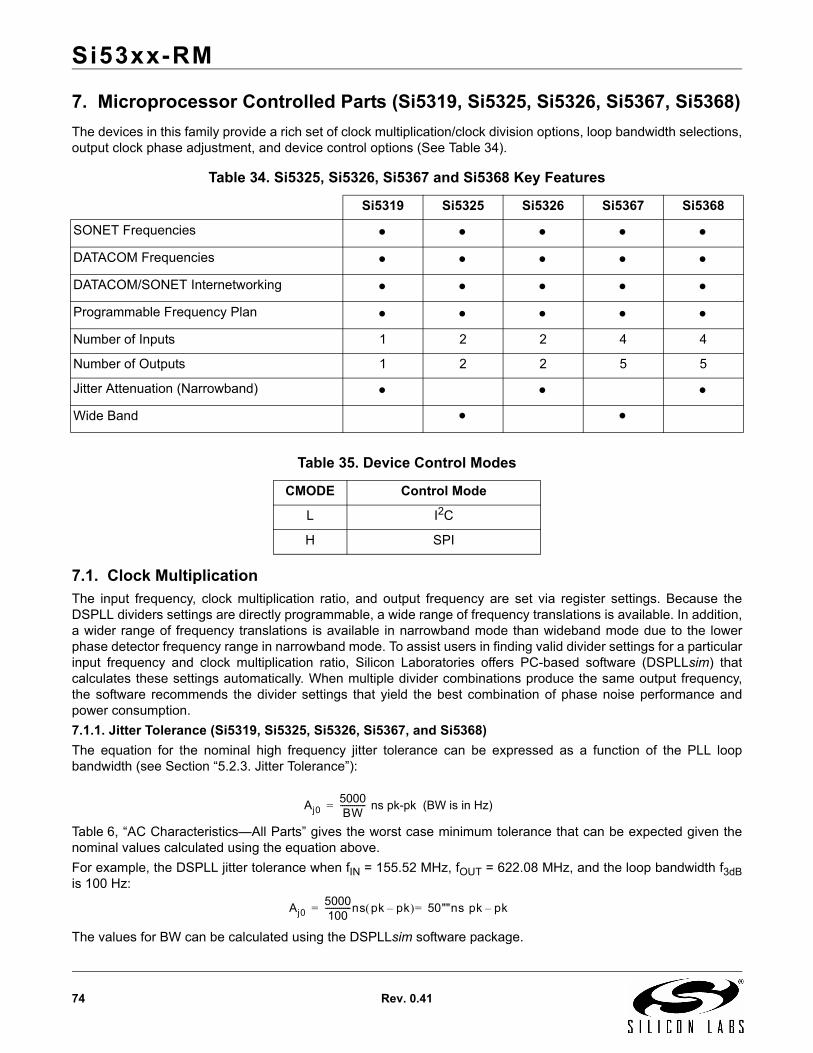
Si53xx-RM
74 Rev. 0.41
7. Microprocessor Controlled Parts (Si5319, Si5325, Si5326, Si5367, Si5368)
The devices in this family provide a rich set of clock multiplication/clock division options, loop bandwidth selections,output clock phase adjustment, and device control options (See Table 34).
7.1. Clock Multiplication The input frequency, clock multiplication ratio, and output frequency are set via register settings. Because theDSPLL dividers settings are directly programmable, a wide range of frequency translations is available. In addition,a wider range of frequency translations is available in narrowband mode than wideband mode due to the lowerphase detector frequency range in narrowband mode. To assist users in finding valid divider settings for a particularinput frequency and clock multiplication ratio, Silicon Laboratories offers PC-based software (DSPLLsim) thatcalculates these settings automatically. When multiple divider combinations produce the same output frequency,the software recommends the divider settings that yield the best combination of phase noise performance andpower consumption.
7.1.1. Jitter Tolerance (Si5319, Si5325, Si5326, Si5367, and Si5368)
The equation for the nominal high frequency jitter tolerance can be expressed as a function of the PLL loopbandwidth (see Section “5.2.3. Jitter Tolerance”):
Table 6, “AC Characteristics—All Parts” gives the worst case minimum tolerance that can be expected given thenominal values calculated using the equation above.
For example, the DSPLL jitter tolerance when fIN = 155.52 MHz, fOUT = 622.08 MHz, and the loop bandwidth f3dBis 100 Hz:
The values for BW can be calculated using the DSPLLsim software package.
Table 34. Si5325, Si5326, Si5367 and Si5368 Key Features
Si5319 Si5325 Si5326 Si5367 Si5368
SONET Frequencies
DATACOM Frequencies
DATACOM/SONET Internetworking
Programmable Frequency Plan
Number of Inputs 1 2 2 4 4
Number of Outputs 1 2 2 5 5
Jitter Attenuation (Narrowband)
Wide Band
Table 35. Device Control Modes
CMODE Control Mode
L I2C
H SPI
Aj05000BW
------------- ns pk-pk (BW is in Hz)=
Aj05000100
-------------ns pk pk– 50""ns pk pk–==
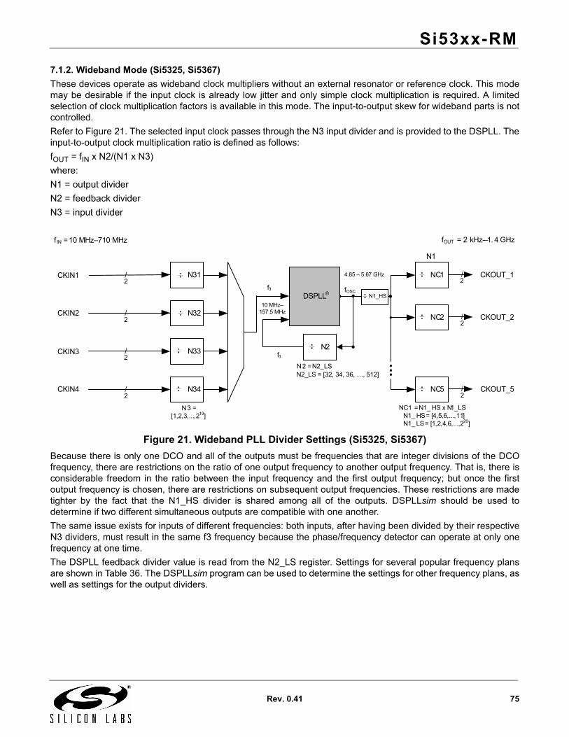
Si53xx-RM
Rev. 0.41 75
7.1.2. Wideband Mode (Si5325, Si5367)
These devices operate as wideband clock multipliers without an external resonator or reference clock. This modemay be desirable if the input clock is already low jitter and only simple clock multiplication is required. A limitedselection of clock multiplication factors is available in this mode. The input-to-output skew for wideband parts is notcontrolled.
Refer to Figure 21. The selected input clock passes through the N3 input divider and is provided to the DSPLL. Theinput-to-output clock multiplication ratio is defined as follows:
fOUT = fIN x N2/(N1 x N3)
where:
N1 = output divider
N2 = feedback divider
N3 = input divider
Figure 21. Wideband PLL Divider Settings (Si5325, Si5367)
Because there is only one DCO and all of the outputs must be frequencies that are integer divisions of the DCOfrequency, there are restrictions on the ratio of one output frequency to another output frequency. That is, there isconsiderable freedom in the ratio between the input frequency and the first output frequency; but once the firstoutput frequency is chosen, there are restrictions on subsequent output frequencies. These restrictions are madetighter by the fact that the N1_HS divider is shared among all of the outputs. DSPLLsim should be used todetermine if two different simultaneous outputs are compatible with one another.
The same issue exists for inputs of different frequencies: both inputs, after having been divided by their respectiveN3 dividers, must result in the same f3 frequency because the phase/frequency detector can operate at only onefrequency at one time.
The DSPLL feedback divider value is read from the N2_LS register. Settings for several popular frequency plansare shown in Table 36. The DSPLLsim program can be used to determine the settings for other frequency plans, aswell as settings for the output dividers.
2/CKIN1 N31
/CKIN2 N32
2
2
N2
N2 = N2_LSN2_LS = [32, 34, 36, …, 512]
NC1
NC2
/ CKOUT_1
/ CKOUT_22
4.85 – 5.67 GHz
fIN = 10 MHz–710 MHz
fOUT = 2 kHz -–1. 4 GHz
/CKIN3 N33
/CKIN4 N34
2
2
10 MHz–157.5 MHz
NC1 = N1_ HS x N1_LSN1_ HS = [4,5,6,...,11]N1_ LS = [1,2,4,6,...,220]
NC5 / CKOUT_52
f3
f3
N1
N3 = [1,2,3,...,219]
fOSCDSPLL® N1_HS
Si53xx-RM
76 Rev. 0.41
Example
Assume the input clock rate on CKIN1, CKIN2, CKIN3, and CKIN4 is 19.44 MHz and the desired input-to-outputmultiplication factor is 32, producing an output clock frequency of 622.08 MHz. Using the desired output frequencyvalue, set N1 = 8 (N1_HS = 8 and N1_LS = 1) to put fOSC within its operating range:
fOSC = 622.08 MHz x 8 = 4.98 GHz
Next, set N3 = 1 to keep the phase detector rate within its operating range:
N3 = 1
Substituting these values in the input-to-output frequency multiplication equation and solving for N2 yields:
32 = N2/(8 x 1)
N2 = 256
Therefore,
N1_HS = 8
N1_LS = 1
N2_LS = 256
N3 = 1.
Table 36. Common Divider Settings (Wideband/µP Control Mode - Si5325 and Si5367)
fIN (MHz) fOUT (MHz) N1_HS N1_LS N2_LS N3
19.44 19.44 5 50 250 1
77.76 8 8 256 1
155.52 8 4 256 1
622.08 4 2 256 1
77.76 77.76 8 8 64 1
155.52 8 4 64 1
622.08 4 2 64 1
155.52 155.52 8 4 64 2
622.08 4 2 64 2
622.08 622.08 4 2 40 5
Note: For some input frequency/clock multiplication ratio combinations, multiple divider settings produce the same output frequency. Divider settings listed above are based on Silicon Laboratories’ DSPLLsim software that estimates which divider setting produces the best phase noise performance while minimizing power consumption. See the Register Map documentation for the appropriate write values.
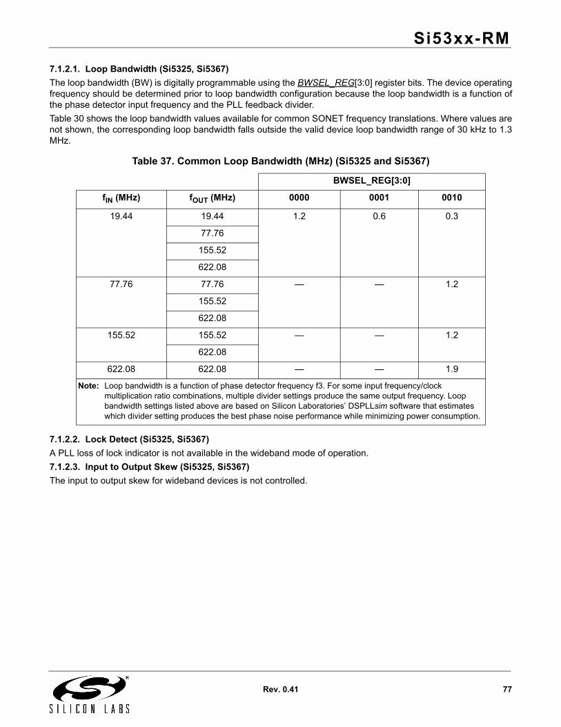
Si53xx-RM
Rev. 0.41 77
7.1.2.1. Loop Bandwidth (Si5325, Si5367)
The loop bandwidth (BW) is digitally programmable using the BWSEL_REG[3:0] register bits. The device operatingfrequency should be determined prior to loop bandwidth configuration because the loop bandwidth is a function ofthe phase detector input frequency and the PLL feedback divider.
Table 30 shows the loop bandwidth values available for common SONET frequency translations. Where values arenot shown, the corresponding loop bandwidth falls outside the valid device loop bandwidth range of 30 kHz to 1.3MHz.
7.1.2.2. Lock Detect (Si5325, Si5367)
A PLL loss of lock indicator is not available in the wideband mode of operation.
7.1.2.3. Input to Output Skew (Si5325, Si5367)
The input to output skew for wideband devices is not controlled.
Table 37. Common Loop Bandwidth (MHz) (Si5325 and Si5367)
BWSEL_REG[3:0]
fIN (MHz) fOUT (MHz) 0000 0001 0010
19.44 19.44 1.2 0.6 0.3
77.76
155.52
622.08
77.76 77.76 — — 1.2
155.52
622.08
155.52 155.52 — — 1.2
622.08
622.08 622.08 — — 1.9
Note: Loop bandwidth is a function of phase detector frequency f3. For some input frequency/clock multiplication ratio combinations, multiple divider settings produce the same output frequency. Loop bandwidth settings listed above are based on Silicon Laboratories’ DSPLLsim software that estimates which divider setting produces the best phase noise performance while minimizing power consumption.
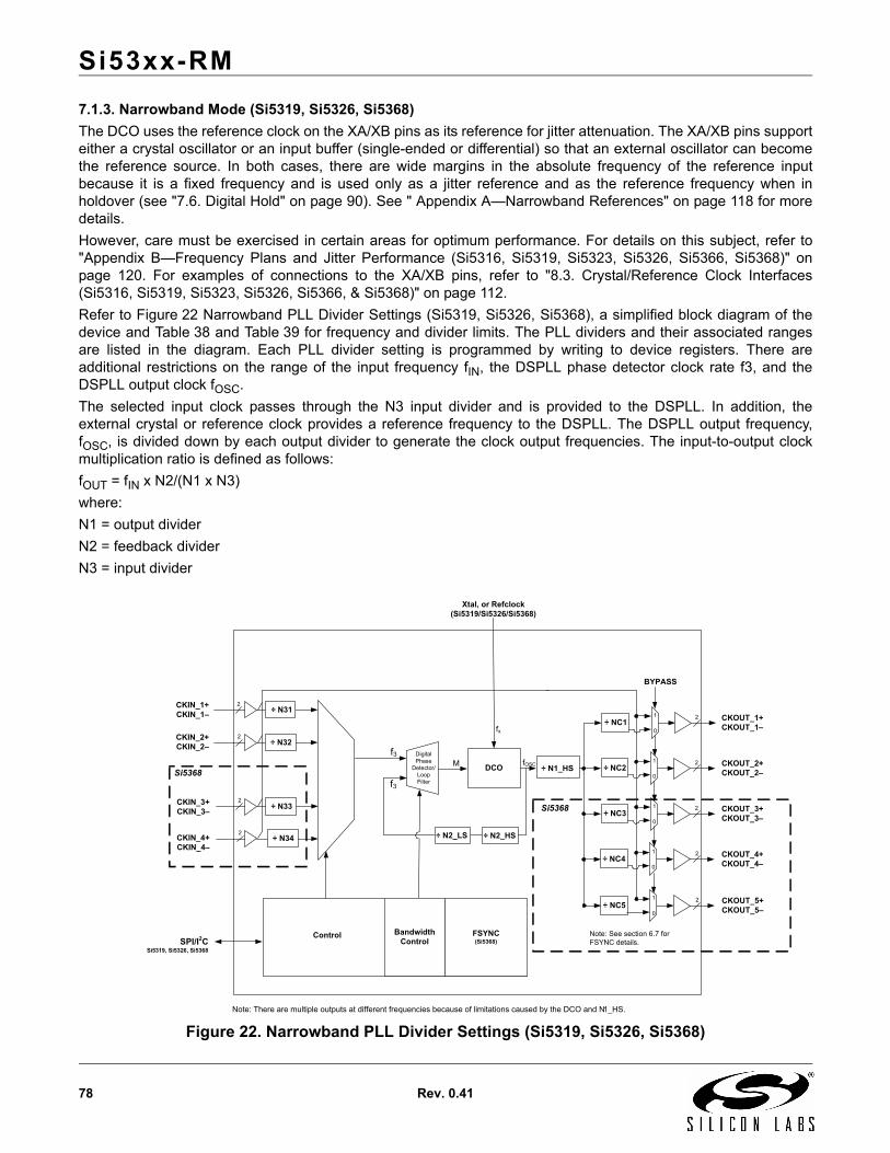
Si53xx-RM
78 Rev. 0.41
7.1.3. Narrowband Mode (Si5319, Si5326, Si5368)
The DCO uses the reference clock on the XA/XB pins as its reference for jitter attenuation. The XA/XB pins supporteither a crystal oscillator or an input buffer (single-ended or differential) so that an external oscillator can becomethe reference source. In both cases, there are wide margins in the absolute frequency of the reference inputbecause it is a fixed frequency and is used only as a jitter reference and as the reference frequency when inholdover (see "7.6. Digital Hold" on page 90). See " Appendix A—Narrowband References" on page 118 for moredetails.
However, care must be exercised in certain areas for optimum performance. For details on this subject, refer to"Appendix B—Frequency Plans and Jitter Performance (Si5316, Si5319, Si5323, Si5326, Si5366, Si5368)" onpage 120. For examples of connections to the XA/XB pins, refer to "8.3. Crystal/Reference Clock Interfaces(Si5316, Si5319, Si5323, Si5326, Si5366, & Si5368)" on page 112.
Refer to Figure 22 Narrowband PLL Divider Settings (Si5319, Si5326, Si5368), a simplified block diagram of thedevice and Table 38 and Table 39 for frequency and divider limits. The PLL dividers and their associated rangesare listed in the diagram. Each PLL divider setting is programmed by writing to device registers. There areadditional restrictions on the range of the input frequency fIN, the DSPLL phase detector clock rate f3, and theDSPLL output clock fOSC.
The selected input clock passes through the N3 input divider and is provided to the DSPLL. In addition, theexternal crystal or reference clock provides a reference frequency to the DSPLL. The DSPLL output frequency,fOSC, is divided down by each output divider to generate the clock output frequencies. The input-to-output clockmultiplication ratio is defined as follows:
fOUT = fIN x N2/(N1 x N3)
where:
N1 = output divider
N2 = feedback divider
N3 = input divider
Figure 22. Narrowband PLL Divider Settings (Si5319, Si5326, Si5368)
CKIN_1+CKIN_1–
CKIN_2+CKIN_2–
CKIN_3+CKIN_3–
CKIN_4+CKIN_4–
CKOUT_1+CKOUT_1–
÷ NC11
0
CKOUT_2+CKOUT_2–
÷ NC21
0
CKOUT_3+CKOUT_3–
÷ NC31
0
CKOUT_4+CKOUT_4–
÷ NC41
0
2
2
2
2
2
2
2
2
DCOfOSC
Xtal, or Refclock(Si5319/Si5326/Si5368)
fx
Mf3 Digital
Phase Detector/
Loop Filter
BYPASS
f3
SPI/I2CSi5319, Si5326, Si5368
Control
÷ N32
÷ N31
Bandwidth Control
FSYNC(Si5368)
Si5368
Si5368
Note: See section 6.7 for FSYNC details.
÷ N1_HS
CKOUT_5+CKOUT_5–
÷ NC51
0
2
÷ N33
÷ N34
Note: There are multiple outputs at different frequencies because of limitations caused by the DCO and N1_HS.
÷ N2_LS ÷ N2_HS
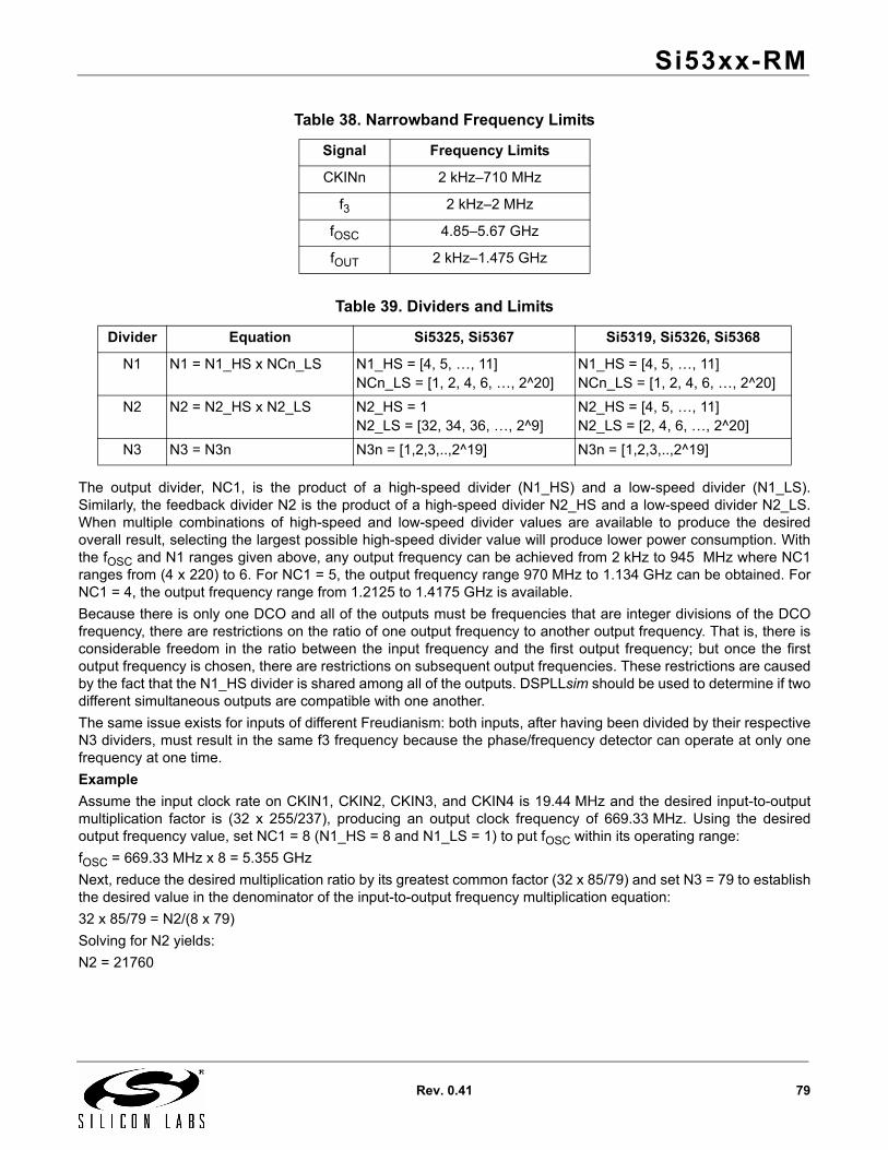
Si53xx-RM
Rev. 0.41 79
The output divider, NC1, is the product of a high-speed divider (N1_HS) and a low-speed divider (N1_LS).Similarly, the feedback divider N2 is the product of a high-speed divider N2_HS and a low-speed divider N2_LS.When multiple combinations of high-speed and low-speed divider values are available to produce the desiredoverall result, selecting the largest possible high-speed divider value will produce lower power consumption. Withthe fOSC and N1 ranges given above, any output frequency can be achieved from 2 kHz to 945 MHz where NC1ranges from (4 x 220) to 6. For NC1 = 5, the output frequency range 970 MHz to 1.134 GHz can be obtained. ForNC1 = 4, the output frequency range from 1.2125 to 1.4175 GHz is available.
Because there is only one DCO and all of the outputs must be frequencies that are integer divisions of the DCOfrequency, there are restrictions on the ratio of one output frequency to another output frequency. That is, there isconsiderable freedom in the ratio between the input frequency and the first output frequency; but once the firstoutput frequency is chosen, there are restrictions on subsequent output frequencies. These restrictions are causedby the fact that the N1_HS divider is shared among all of the outputs. DSPLLsim should be used to determine if twodifferent simultaneous outputs are compatible with one another.
The same issue exists for inputs of different Freudianism: both inputs, after having been divided by their respectiveN3 dividers, must result in the same f3 frequency because the phase/frequency detector can operate at only onefrequency at one time.
Example
Assume the input clock rate on CKIN1, CKIN2, CKIN3, and CKIN4 is 19.44 MHz and the desired input-to-outputmultiplication factor is (32 x 255/237), producing an output clock frequency of 669.33 MHz. Using the desiredoutput frequency value, set NC1 = 8 (N1_HS = 8 and N1_LS = 1) to put fOSC within its operating range:
fOSC = 669.33 MHz x 8 = 5.355 GHz
Next, reduce the desired multiplication ratio by its greatest common factor (32 x 85/79) and set N3 = 79 to establishthe desired value in the denominator of the input-to-output frequency multiplication equation:
32 x 85/79 = N2/(8 x 79)
Solving for N2 yields:
N2 = 21760
Table 38. Narrowband Frequency Limits
Signal Frequency Limits
CKINn 2 kHz–710 MHz
f3 2 kHz–2 MHz
fOSC 4.85–5.67 GHz
fOUT 2 kHz–1.475 GHz
Table 39. Dividers and Limits
Divider Equation Si5325, Si5367 Si5319, Si5326, Si5368
N1 N1 = N1_HS x NCn_LS N1_HS = [4, 5, …, 11]NCn_LS = [1, 2, 4, 6, …, 2^20]
N1_HS = [4, 5, …, 11]NCn_LS = [1, 2, 4, 6, …, 2^20]
N2 N2 = N2_HS x N2_LS N2_HS = 1N2_LS = [32, 34, 36, …, 2^9]
N2_HS = [4, 5, …, 11]N2_LS = [2, 4, 6, …, 2^20]
N3 N3 = N3n N3n = [1,2,3,..,2^19] N3n = [1,2,3,..,2^19]
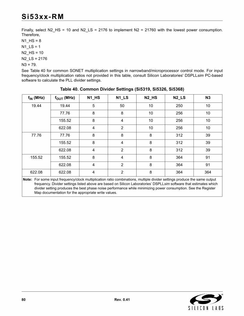
Si53xx-RM
80 Rev. 0.41
Finally, select N2_HS = 10 and N2_LS = 2176 to implement N2 = 21760 with the lowest power consumption.Therefore,
N1_HS = 8
N1_LS = 1
N2_HS = 10
N2_LS = 2176
N3 = 79.
See Table 40 for common SONET multiplication settings in narrowband/microprocessor control mode. For inputfrequency/clock multiplication ratios not provided in this table, consult Silicon Laboratories' DSPLLsim PC-basedsoftware to calculate the PLL divider settings.
Table 40. Common Divider Settings (Si5319, Si5326, Si5368)
fIN (MHz) fOUT (MHz) N1_HS N1_LS N2_HS N2_LS N3
19.44 19.44 5 50 10 250 10
77.76 8 8 10 256 10
155.52 8 4 10 256 10
622.08 4 2 10 256 10
77.76 77.76 8 8 8 312 39
155.52 8 4 8 312 39
622.08 4 2 8 312 39
155.52 155.52 8 4 8 364 91
622.08 4 2 8 364 91
622.08 622.08 4 2 8 364 364
Note: For some input frequency/clock multiplication ratio combinations, multiple divider settings produce the same output frequency. Divider settings listed above are based on Silicon Laboratories’ DSPLLsim software that estimates which divider setting produces the best phase noise performance while minimizing power consumption. See the Register Map documentation for the appropriate write values.
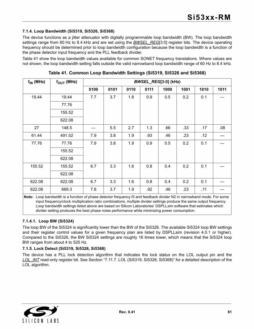
Si53xx-RM
Rev. 0.41 81
7.1.4. Loop Bandwidth (Si5319, Si5326, Si5368)
The device functions as a jitter attenuator with digitally programmable loop bandwidth (BW). The loop bandwidthsettings range from 60 Hz to 8.4 kHz and are set using the BWSEL_REG[3:0] register bits. The device operatingfrequency should be determined prior to loop bandwidth configuration because the loop bandwidth is a function ofthe phase detector input frequency and the PLL feedback divider.
Table 41 show the loop bandwidth values available for common SONET frequency translations. Where values arenot shown, the loop bandwidth setting falls outside the valid narrowband loop bandwidth range of 60 Hz to 8.4 kHz.
7.1.4.1. Loop BW (Si5324)
The loop BW of the Si5324 is significantly lower than the BW of the Si5326. The available Si5324 loop BW settingsand their register control values for a given frequency plan are listed by DSPLLsim (revision 4.0.1 or higher).Compared to the Si5326, the BW Si5324 settings are roughly 16 times lower, which means that the Si5324 loopBW ranges from about 4 to 525 Hz.
7.1.5. Lock Detect (Si5319, Si5326, Si5368)
The device has a PLL lock detection algorithm that indicates the lock status on the LOL output pin and theLOL_INT read-only register bit. See Section “7.11.7. LOL (Si5319, Si5326, Si5368)” for a detailed description of theLOL algorithm.
Table 41. Common Loop Bandwidth Settings (Si5319, Si5326 and Si5368)
fIN (MHz) fOUT (MHz) BWSEL_REG[3:0] (kHz)
0100 0101 0110 0111 1000 1001 1010 1011
19.44 19.44 7.7 3.7 1.8 0.9 0.5 0.2 0.1 —
77.76
155.52
622.08
27 148.5 — 5.5 2.7 1.3 .66 .33 .17 .08
61.44 491.52 7.9 3.8 1.9 .93 .46 .23 .12 —
77.76 77.76 7.9 3.8 1.9 0.9 0.5 0.2 0.1 —
155.52
622.08
155.52 155.52 6.7 3.3 1.6 0.8 0.4 0.2 0.1 —
622.08
622.08 622.08 6.7 3.3 1.6 0.8 0.4 0.2 0.1 —
622.08 669.3 7.8 3.7 1.9 .92 .46 .23 .11 —
Note: Loop bandwidth is a function of phase detector frequency f3 and feedback divider N2 in narrowband mode. For some input frequency/clock multiplication ratio combinations, multiple divider settings produce the same output frequency. Loop bandwidth settings listed above are based on Silicon Laboratories’ DSPLLsim software that estimates which divider setting produces the best phase noise performance while minimizing power consumption.
Si53xx-RM
82 Rev. 0.41
7.2. PLL Self-CalibrationThe device performs an internal self-calibration before operation to optimize loop parameters and jitterperformance. While the self-calibration is being performed, the DCO is being internally controlled by the self-calibration state machine, and the LOL alarm will be active. The output clocks can either be active or disableddepending on the SQ_ICAL bit setting. The self-calibration time tLOCKHW is given in Table 6, “AC Characteristics—All Parts”. The procedure for initiating the internal self-calibration is described below.
7.2.1. Initiating Internal Self-Calibration
Any of the following events will trigger an automatic self-calibration:
Exit from SLEEP mode
Internal DCO registers out-of-range, indicating the need to relock the DCO
Setting the ICAL register bit to 1
In any of the above cases, an internal self-calibration will be initiated if a valid input clock exists (no input alarm)and is selected as the active clock at that time. The external crystal or reference clock must also be present for theself-calibration to begin (LOSX_INT = 0 [narrowband only]).
When self-calibration is initiated the device generates an output clock if the SQ_ICAL bit is set to 0. The outputclock will appear when the device begins self-calibration. The frequency of the output clocks may be as high as 5%above or as low as 20% below the final locked value. If SQ_ICAL = 1, the output clocks are disabled during self-calibration and will appear after the self-calibration routine is completed.
After a successful self-calibration has been performed with a valid input clock, it is not necessary to reinitiate a self-calibration for subsequent losses of input clock. If the input clock is lost following self-calibration, the device entersdigital hold mode. When the input clock returns, the device relocks to the input clock without performing a self-calibration.
After power-up and writing of dividers or PLL registers, the user must set ICAL = 1 to initiate a self-calibration. LOLwill go low when self calibration is complete. Depending on the selected value of the loop BW, it may take a fewseconds more for the output frequency and phase to completely settle.
7.2.1.1. PLL Self-Calibration
Due to the low loop BW of the Si5324, the lock time of the Si5324 is significantly longer than the lock time of theSi5326. As a method of reducing the lock time, a FAST_LOCK register bit was added to the Si5324. As the Si5324data sheet indicates, FAST_LOCK is the LSB of register 137. When FAST_LOCK is high, the lock time decreases.Because the Si5324 is initialized with FAST_LOCK low, it must be written before ICAL is set. Note that the LockTime specification in Table 6 on page 33 of the FRM does not apply to the Si5324, with or without FAST_LOCK.Typical Si5324 lock times (as defined from the start of ICAL until LOL going low) with FAST_LOCK set are 60seconds.
7.2.2. Input Clock Stability during Internal Self-Calibration
An ICAL must occur when the selected active CKINn clock is stable in frequency and with a frequency value that iswithin the operating range that is reported by DSPLLsim. The other CKINs must be stable in frequency (< 100 ppmfrom nominal) or squelched during an ICAL.
7.2.3. Self-Calibration Caused by Changes in Input Frequency
If the selected CKINn varies by 500 ppm or more in frequency since the last calibration, the device may initiate aself-calibration.
7.2.4. Narrowband Input-to-Output Skew (Si5319, Si5326, Si5368)
The input-to-output skew is not controlled. External circuitry is required to control the input-to-output skew. ContactSilicon Labs for further information.
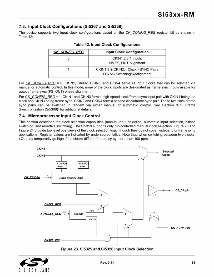
Si53xx-RM
Rev. 0.41 83
7.3. Input Clock Configurations (Si5367 and Si5368)The device supports two input clock configurations based on the CK_CONFIG_REG register bit as shown inTable 42:
For CK_CONFIG_REG = 0, CKIN1, CKIN2, CKIN3, and CKIN4 serve as input clocks that can be selected viamanual or automatic control. In this mode, none of the clock inputs are designated as frame sync inputs usable foroutput frame sync (FS_OUT) phase alignment.
For CK_CONFIG_REG = 1, CKIN1 and CKIN3 form a high-speed clock/frame sync input pair with CKIN1 being theclock and CKIN3 being frame sync. CKIN2 and CKIN4 form a second clock/frame sync pair. These two clock/framesync pairs can be switched in tandem via either manual or automatic control. See Section “6.5. FrameSynchronization (Si5366)” for additional details.
7.4. Microprocessor Input Clock ControlThis section describes the clock selection capabilities (manual input selection, automatic input selection, hitlessswitching, and revertive switching). The Si5319 supports only pin-controlled manual clock selection. Figure 23 andFigure 24 provide top level overviews of the clock selection logic, though they do not cover wideband or frame syncapplications. Register values are indicated by underscored italics. Note that, when switching between two clocks,LOL may temporarily go high if the clocks differ in frequency by more than 100 ppm.
Figure 23. Si5325 and Si5326 Input Clock Selection
Table 42. Input Clock Configurations
CK_CONFIG_REG Input Clock Configuration
0 CKIN1,2,3,4 InputsNo FS_OUT Alignment
1 CKIN1,3 & CKIN2,4 Clock/FSYNC PairsFSYNC Switching/Realignment
CKIN1
CKIN2
Clock priority logicCK_PRIORn
0
1
CKSEL_REG
AUTOSEL_REG 0
1
CKSEL_PIN
LOS/FOSdetectLOS/FOSdetect
LOS/FOSdetectLOS/FOSdetect
decodeAuto
Manual
SelectedClock
2
4
CS_CA pin
CK_ACTV_PIN
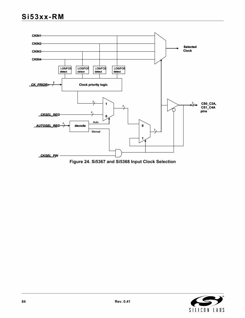
Si53xx-RM
84 Rev. 0.41
Figure 24. Si5367 and Si5368 Input Clock Selection
CKIN1
CKIN2
CKIN3
CKIN4
Clock priority logicCK_PRIORn
0
1
CKSEL_REG
AUTOSEL_REG 0
1
CKSEL_PIN
LOS/FOSdetect
LOS/FOSdetect
LOS/FOSdetect
LOS/FOSdetect
decodeAuto
Manual
SelectedClock
2
2
2
2
2
8
2 CS0_C3A,CS1_C4Apins
CKIN1
CKIN2
CKIN3
CKIN4
Clock priority logicCK_PRIORn
0
1
CKSEL_REG
AUTOSEL_REG 0
1
CKSEL_PIN
LOS/FOSdetectLOS/FOSdetect
LOS/FOSdetectLOS/FOSdetect
LOS/FOSdetectLOS/FOSdetect
LOS/FOSdetectLOS/FOSdetect
decodeAuto
Manual
SelectedClock
2
2
2
2
2
8
2 CS0_C3A,CS1_C4Apins
Si53xx-RM
Rev. 0.41 85
7.4.1. Manual Clock Selection
Manual control of input clock selection is available by setting the AUTOSEL_REG[1:0] register bits to 00. In manualmode, the active input clock is chosen via the CKSEL_REG[1:0] register setting according to Table 43 andTable 44.
If the selected clock enters an alarm condition, the PLL enters digital hold mode. The CKSEL_REG[1:0] controlsare ignored if automatic clock selection is enabled.
7.4.2. Automatic Clock Selection
The AUTOSEL_REG[1:0] register bits sets the input clock selection mode as shown in Table 45. Automaticswitching is either revertive or non-revertive.
CKSEL_PIN is of significance only when Manual is selected.
Table 43. Manual Input Clock Selection (Si5367, Si5368)
CKSEL_REG[1:0] Register Bits
Active Input Clock
CK_CONFIG_REG = 0(CKIN1,2,3,4 inputs)
CK_CONFIG_REG = 1(CKIN1,3 & CKIN2,4 clock/FSYNC pairs)
00 CKIN1 CKIN1/CKIN3
01 CKIN2 CKIN2/CKIN4
10 CKIN3 Not used
11 CKIN4 Not used
Note: Setting the CKSEL_PIN register bit to one allows the CS [1:0] pins to continue to control input clock selection. If CS_PIN is set to zero, the CKSEL_REG[1:0] register bits perform the input clock selection function.
Table 44. Manual Input Clock Selection (Si5325, Si5326)
CKSEL_REG or CS pin Active Input Clock
0 CKIN1
1 CKIN2
Table 45. Automatic/Manual Clock Selection
AUTOSEL_REG[1:0] Clock Selection Mode
00 Manual
01 Automatic Non-revertive
10 Automatic Revertive
11 Reserved
Si53xx-RM
86 Rev. 0.41
7.4.2.1. Detailed Automatic Clock Selection Description (Si5325, Si5326)
Automatic switching is either revertive or non-revertive. The default prioritization of clock inputs when the device isconfigured for automatic switching operation is CKIN1, followed by CKIN2, and finally, digital hold mode. Theinverse input clock priority arrangement is available through the CK_PRIOR bits, as shown in the Si5325 andSi5326 Register Maps.
For the default priority arrangement, automatic switching mode selects CKIN1 at powerup, reset, or when inrevertive mode with no alarms present on CKIN1. If an alarm condition occurs on CKIN1 and there are no activealarms on CKIN2, then the device switches to CKIN2. If both CKIN1 and CKIN2 are alarmed, then the deviceenters digital hold mode. If automatic mode and microprocessor control mode are selected and the frequencyoffset alarms (FOS1_INT and FOS2_INT) are disabled, automatic switching is not initiated in response to FOSalarms. The loss-of-signal alarms (LOS1_INT and LOS2_INT) are always used in making automatic clock selectionchoices.
In non-revertive mode, once CKIN2 is selected, CKIN2 selection remains as long as it is valid even if alarms arecleared on CKIN1.
7.4.2.2. Detailed Automatic Clock Selection Description (Si5367, Si5368)
The prioritization of clock inputs for automatic switching is shown in Table 46. For example, ifCK_CONFIG_REG = 0 and the desired clock priority order is CKIN4, CKIN3, CKIN2, and then CKIN1 as thelowest priority clock, the user should set CK_PRIOR1[1:0] = 11, CK_PRIOR2[1:0] = 10, CK_PRIOR3[1:0] = 01, andCK_PRIOR4[1:0] = 00.
If CK_CONFIG_REG = 1 and the desired clock priority is CKIN1/CKIN3 and then CKIN2/CKIN4, the user shouldset CK_PRIOR1[1:0] = 00 and CK_PRIOR2[1:0] = 01 (CK_PRIOR3[1:0] and CK_PRIOR4[1:0] are ignored in thiscase).
The following discussion describes the clock selection algorithm for the case of four possible input clocks(CK_CONFIG_REG = 0) in the default priority arrangement (priority order CKIN1, CKIN2, CKIN3, CKIN4).Automatic switching mode selects CKIN1 at powerup, reset, or when in revertive mode with no alarms present onCKIN1. If an alarm condition occurs on CKIN1 and there are no active alarms on CKIN2, the device switches toCKIN2. If both CKIN1 and CKIN2 are alarmed and there is no alarm on CKIN3, the device switches to CKIN3. IfCKIN1, CKIN2, and CKIN3 are alarmed and there is no alarm on CKIN4, the device switches to CKIN4. If alarmsexist on CKIN1, CKIN2, CKIN3, and CKIN4, the device enters digital hold mode. If automatic mode is selected andthe frequency offset alarms (FOS1_INT, FOS2_INT, FOS3_INT, FOS4_INT) are disabled, automatic switching isnot initiated in response to FOS alarms. The loss-of-signal alarms (LOS1_INT, LOS2_INT, LOS3_INT, LOS4_INT)are always used in making automatic clock selection choices. In non-revertive mode, once CKIN2 is selected,CKIN2 selection remains as long as it is valid even if alarms are cleared on CKIN1.
Table 46. Input Clock Priority for Auto Switching in µP Control Mode
Selected Clock
CK_PRIORn[1:0] CK_CONFIG_REG = 0 CK_CONFIG_REG = 1
00 CKIN1 CKIN1/CKIN3
01 CKIN2 CKIN2/CKIN4
10 CKIN3 Not Used
11 CKIN4 Not Used
Si53xx-RM
Rev. 0.41 87
7.4.3. Hitless Switching with Phase Build-Out (Si5326, Si5368)
Silicon Laboratories switching technology performs phase build-out, which maintains the phase of the output whenthe input clock is switched. This minimizes the propagation of phase transients to the clock outputs during inputclock switching. All switching between input clocks occurs within the input multiplexer and phase detector circuitry.The phase detector circuitry continually monitors the phase difference between each input clock and the DSPLLoutput clock, fOSC. The phase detector circuitry can lock to a clock signal at a specified phase offset relative to fOSCso that the phase offset is maintained by the PLL circuitry.
At the time a clock switch occurs, the phase detector circuitry knows both the input-to-output phase relationship forthe original input clock and for the new input clock. The phase detector circuitry locks to the new input clock at thenew clock's phase offset so that the phase of the output clock is not disturbed. The phase difference between thetwo input clocks is absorbed in the phase detector's offset value, rather than being propagated to the clock output.
The switching technology virtually eliminates the output clock phase transients traditionally associated with clockrearrangement (input clock switching). The wander and maximum slope for clock output phase transients duringclock switching are given in Table 6, “AC Characteristics—All Parts”. These values fall significantly below the limitsspecified in the Telcordia GR-1244-CORE and GR-253-CORE requirements.
Note that hitless switching between input clocks applies only when the input clock validation time isVALTIME[1:0] = 01 or higher.
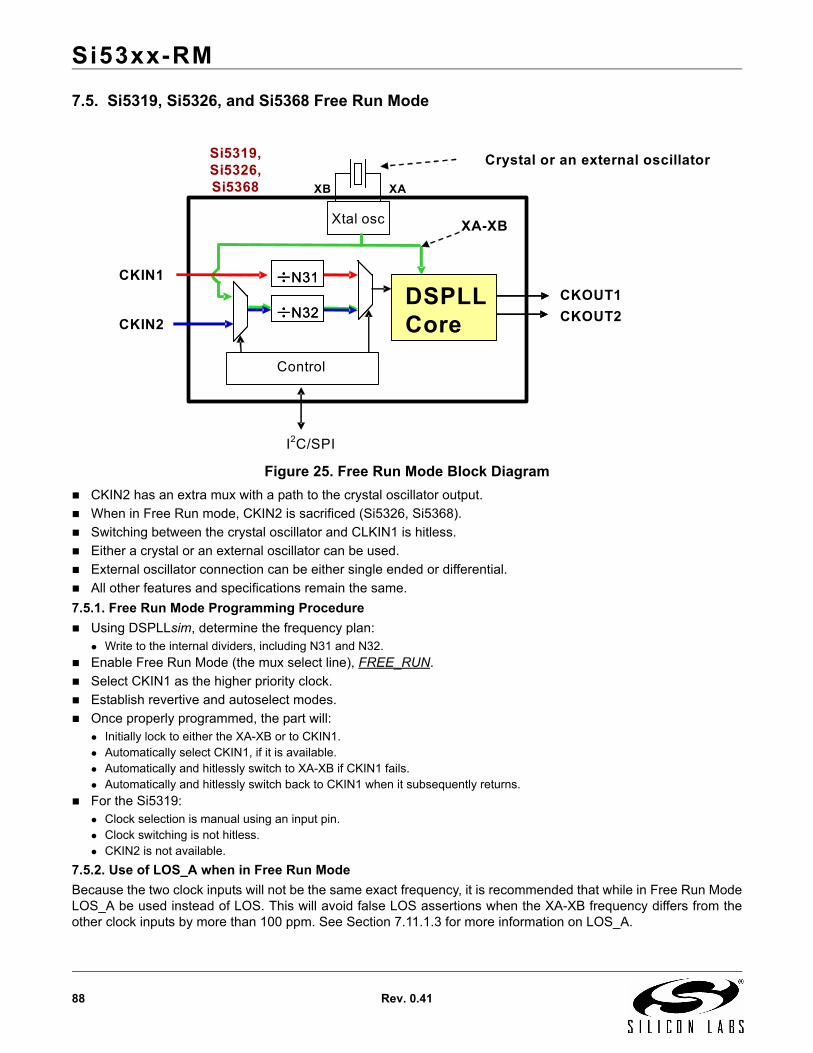
Si53xx-RM
88 Rev. 0.41
7.5. Si5319, Si5326, and Si5368 Free Run Mode
Figure 25. Free Run Mode Block Diagram
CKIN2 has an extra mux with a path to the crystal oscillator output.
When in Free Run mode, CKIN2 is sacrificed (Si5326, Si5368).
Switching between the crystal oscillator and CLKIN1 is hitless.
Either a crystal or an external oscillator can be used.
External oscillator connection can be either single ended or differential.
All other features and specifications remain the same.
7.5.1. Free Run Mode Programming Procedure
Using DSPLLsim, determine the frequency plan:Write to the internal dividers, including N31 and N32.
Enable Free Run Mode (the mux select line), FREE_RUN.
Select CKIN1 as the higher priority clock.
Establish revertive and autoselect modes.
Once properly programmed, the part will:Initially lock to either the XA-XB or to CKIN1.Automatically select CKIN1, if it is available.Automatically and hitlessly switch to XA-XB if CKIN1 fails.Automatically and hitlessly switch back to CKIN1 when it subsequently returns.
For the Si5319:Clock selection is manual using an input pin.Clock switching is not hitless.CKIN2 is not available.
7.5.2. Use of LOS_A when in Free Run Mode
Because the two clock inputs will not be the same exact frequency, it is recommended that while in Free Run ModeLOS_A be used instead of LOS. This will avoid false LOS assertions when the XA-XB frequency differs from theother clock inputs by more than 100 ppm. See Section 7.11.1.3 for more information on LOS_A.
Crystal or an external oscillatorSi5319, Si5326,Si5368
CKOUT1
CKOUT2
Xtal osc
DSPLL Core
CKIN1
I2C/SPI
CKIN2
Control
XA-XB
N31N31
N32N32
XAXB
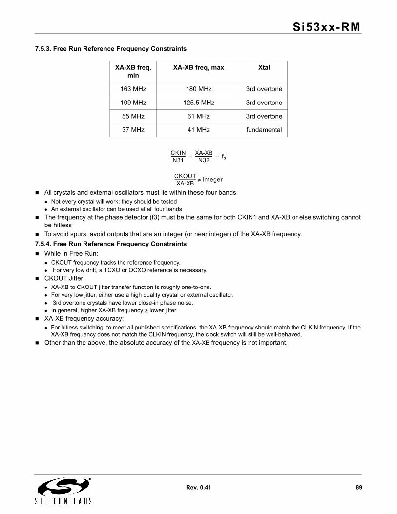
Si53xx-RM
Rev. 0.41 89
7.5.3. Free Run Reference Frequency Constraints
All crystals and external oscillators must lie within these four bandsNot every crystal will work; they should be testedAn external oscillator can be used at all four bands
The frequency at the phase detector (f3) must be the same for both CKIN1 and XA-XB or else switching cannot be hitless
To avoid spurs, avoid outputs that are an integer (or near integer) of the XA-XB frequency.
7.5.4. Free Run Reference Frequency Constraints
While in Free Run:CKOUT frequency tracks the reference frequency. For very low drift, a TCXO or OCXO reference is necessary.
CKOUT Jitter:XA-XB to CKOUT jitter transfer function is roughly one-to-one.For very low jitter, either use a high quality crystal or external oscillator. 3rd overtone crystals have lower close-in phase noise.In general, higher XA-XB frequency > lower jitter.
XA-XB frequency accuracy:For hitless switching, to meet all published specifications, the XA-XB frequency should match the CLKIN frequency. If the
XA-XB frequency does not match the CLKIN frequency, the clock switch will still be well-behaved.
Other than the above, the absolute accuracy of the XA-XB frequency is not important.
XA-XB freq, min
XA-XB freq, max Xtal
163 MHz 180 MHz 3rd overtone
109 MHz 125.5 MHz 3rd overtone
55 MHz 61 MHz 3rd overtone
37 MHz 41 MHz fundamental
CKINN31
--------------- XA-XBN32
------------------ f3= =
CKOUTXA-XB
---------------------- Integer
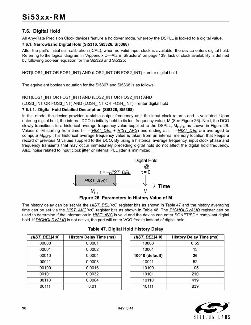
Si53xx-RM
90 Rev. 0.41
7.6. Digital HoldAll Any-Rate Precision Clock devices feature a holdover mode, whereby the DSPLL is locked to a digital value.
7.6.1. Narrowband Digital Hold (Si5316, Si5326, Si5368)
After the part's initial self-calibration (ICAL), when no valid input clock is available, the device enters digital hold.Referring to the logical diagram in "Appendix D—Alarm Structure" on page 139, lack of clock availability is definedby following boolean equation for the Si5326 and Si5325:
NOT(LOS1_INT OR FOS1_INT) AND (LOS2_INT OR FOS2_INT) = enter digital hold
The equivalent boolean equation for the Si5367 and Si5368 is as follows:
NOT(LOS1_INT OR FOS1_INT) AND (LOS2_INT OR FOS2_INT) AND
(LOS3_INT OR FOS3_INT) AND (LOS4_INT OR FOS4_INT) = enter digital hold
7.6.1.1. Digital Hold Detailed Description (Si5326, Si5368)
In this mode, the device provides a stable output frequency until the input clock returns and is validated. Uponentering digital hold, the internal DCO is initially held to its last frequency value, M (See Figure 26). Next, the DCOslowly transitions to a historical average frequency value supplied to the DSPLL, MHIST, as shown in Figure 26.Values of M starting from time t = –(HIST_DEL + HIST_AVG) and ending at t = –HIST_DEL are averaged tocompute MHIST. This historical average frequency value is taken from an internal memory location that keeps arecord of previous M values supplied to the DCO. By using a historical average frequency, input clock phase andfrequency transients that may occur immediately preceding digital hold do not affect the digital hold frequency.Also, noise related to input clock jitter or internal PLL jitter is minimized.
Figure 26. Parameters in History Value of M
The history delay can be set via the HIST_DEL[4:0] register bits as shown in Table 47 and the history averagingtime can be set via the HIST_AVG[4:0] register bits as shown in Table 48. The DIGHOLDVALID register can beused to determine if the information in HIST_AVG is valid and the device can enter SONET/SDH compliant digitalhold. If DIGHOLDVALID is not active, the part will enter VCO freeze instead of digital hold.
Table 47. Digital Hold History Delay
HIST_DEL[4:0] History Delay Time (ms) HIST_DEL[4:0] History Delay Time (ms)
00000 0.0001 10000 6.55
00001 0.0002 10001 13
00010 0.0004 10010 (default) 26
00011 0.0008 10011 52
00100 0.0016 10100 105
00101 0.0032 10101 210
00110 0.0064 10110 419
00111 0.01 10111 839
Time
Digital Hold @
t = 0
MMHIST
t = –HIST_DEL
HIST_AVG
Si53xx-RM
Rev. 0.41 91
If a highly stable reference, such as an oven-controlled crystal oscillator (OCXO) is supplied at XA/XB, anextremely stable digital hold can be achieved. If a crystal is supplied at the XA/XB port, the digital hold stability willbe limited by the stability of the crystal. Table 6, “AC Characteristics—All Parts” gives the specifications related tothe digital hold function.
7.6.2. Recovery from Digital Hold (Si5319, Si5326, Si5368)
When the input clock signal returns, the device transitions from digital hold to the selected input clock. The deviceperforms hitless recovery from digital hold. The clock transition from digital hold to the returned input clock includes"phase buildout" to absorb the phase difference between the digital hold clock phase and the input clock phase.
01000 0.03 11000 1678
01001 0.05 11001 3355
01010 0.10 11010 6711
01011 0.20 11011 13422
01100 0.41 11100 26844
01101 0.82 11101 53687
01110 1.64 11110 107374
01111 3.28 11111 214748
Table 48. Digital Hold History Averaging Time
HIST_AVG[4:0] History Averaging Time (ms) HIST_AVG[4:0] History Averaging Time (ms)
00000 0.0000 10000 26
00001 0.0004 10001 52
00010 0.001 10010 105
00011 0.003 10011 210
00100 0.006 10100 419
00101 0.012 10101 839
00110 0.03 10110 1678
00111 0.05 10111 3355
01000 0.10 11000 (default) 6711
01001 0.20 11001 13422
01010 0.41 11010 26844
01011 0.82 11011 53687
01100 1.64 11100 107374
01101 3.28 11101 214748
01110 6.55 11110 429497
01111 13 11111 858993
Table 47. Digital Hold History Delay (Continued)
HIST_DEL[4:0] History Delay Time (ms) HIST_DEL[4:0] History Delay Time (ms)
Si53xx-RM
92 Rev. 0.41
7.6.3. VCO Freeze (Si5319, Si5325, Si5367)
If an LOS or FOS condition exists on the selected input clock, the device enters VCO freeze. In this mode, thedevice provides a stable output frequency until the input clock returns and is validated. When the device entersdigital hold, the internal oscillator is initially held to its last frequency value. VCO freeze is not compliant withSONET/SDH MTIE requirements; applications requiring SONET/SDH MTIE requirements should use the Si5326or Si5368. Unlike the Si5325 and Si5367, the Si5319’s VCO freeze is controlled by the XA-XB reference (which istypically a crystal) for greater stability. For the Si5319, VCO freeze is similar to the Digital Hold function of theSi5326 and Si5368, except that the HIST_AVG and HIST_DEL registers do not exist.
7.7. Output Phase Adjust (Si5326, Si5368)The device has a highly accurate, digitally controlled device skew capability. For more information on Output PhaseAdjustments, see both DSPLLsim and the Register Maps. Both can be downloaded by going to www.silabs.com/timing and clicking on “Documentation” at the bottom of the page.
7.7.1. Coarse Skew Control (Si5326, Si5368)
With the INCDEC_PIN register bit set to 0 (pin control off), overall device skew is controlled via the CLAT[7:0]register bits. This skew control has a resolution of 1/fOSC, approximately 200 ps, and a range from –25.6 to25.4 ns. Following a powerup or reset (RST pin or RST_REG register bit), the skew will revert to the reset valueand then the value in the CLAT register will be read and automatically applied to the outputs. Any further changesmade in the skew register will be read and compared to the previously held value. The difference will be calculatedand applied to the clock outputs. All skew changes are made in a glitch-free fashion.
When a phase adjustment is in progress, any new CLAT[7:0] values are ignored until the update is complete. TheCLATPROG register bit is set to 1 during a coarse skew adjustment. Table 6, “AC Characteristics—All Parts”specifies the maximum amount of time required to complete a coarse skew phase adjustment. To verify a writtenvalue into CLAT, the CLAT register should be read after the register is written. The time that it takes for the effectsof a CLAT change to complete is proportional to the size of the change, at 83.3 msec for every unit change. Forexample, if CLAT is zero and has the value 100 written to it, the changes will complete in 100 x 83.3 msec = 8.33 sec.
If it is necessary to set the high-speed output clock divider N1_HS to divide-by-4 in order to achieve the desiredoverall multiplication ratio and output frequency, only phase increments are allowed and negative settings in theCLAT register or attempts to decrement the phase via writes to the CLAT register will be ignored. Because of thisrestriction, when there is a choice between using N1_HS = 4 and another N1_HS value that can produce thedesired multiplication ratio, the other N1_HS value should be selected. This restriction also applies when using theINC pin.
With the INCDEC_PIN register bit set to 1 (pin control on), the INC and DEC pins function the same as they do forpin controlled parts. See "6.6. Output Phase Adjust (Si5323, Si5366)" on page 69.
7.7.1.1. Unlimited Coarse Skew Adjustment (Si5326, Si5368)
Using the following procedure, the CLAT register can be used to adjust the device clock output phase to anarbitrarily large value that is not limited by the size of the CLAT register:
1. Write a phase adjustment value to the CLAT register (register 16). The DSPLLsim configuration software provides the size of a single step.
2. Wait until CLATPROGRESS = 0 (register 130, bit 7), which indicates that the adjustment is complete (Maximum time for adjustment: 20 seconds for the Si5326 or Si5368).
3. Set INCDEC_PIN = 1 (register 21, bit 7).
4. Write 0 to CLAT register (register 16).
5. Wait until CLATPROGRESS = 0.
6. Set INCDEC_PIN=0.
7. Repeat the above process as many times as desired.
Steps 3-6 will clear the CLAT register without changing the output phase. This allows for unlimited output clockphase adjustment using the CLAT register and repeating steps 1-3 as many times as needed.
Si53xx-RM
Rev. 0.41 93
7.7.2. Fine Skew Control (Si5326, Si5368)
An additional fine adjustment of the overall device skew can be used in conjunction with the INC and DEC pins orthe CLAT[7:0] register bits to provide finer resolution output phase adjustments. Fine phase adjustment is availableusing the FLAT[14:0] bits. The nominal range and resolution of the FLAT[14:0] skew adjustment word are:
Range FLAT = ±110 ps
Resolution FLAT = 9 ps
Before writing a new FLAT[14:0] value, the FLAT_VALID bit must be set to 0 to hold the existing FLAT[14:0] valuewhile the new value is being written. Once the new value is written, set FLAT_VALID = 1 to enable its use.
Table 6, “AC Characteristics—All Parts” specifies the maximum amount of time required to complete a FLAT phaseadjustment. To verify a written value into FLAT, the FLAT register should be read after the register is written.
Because the FLAT resolution varies with the frequency plan and selected bandwidth, DSPLLsim reports the FLATresolution each time it creates a new frequency plan.
7.7.2.1. Output Phase Adjust (Si5324)
Because of its low loop BW, the output phase of the Si5324 is not adjustable. This means that the Si5324 does nothave any INC or DEC pins and that it does not have CLAT or FLAT registers.
7.7.3. Independent Skew (Si5326, Si5368)
The phase of each clock output may be adjusted in relation to the phase of the other clock outputs, respectively.This feature is available when CK_CONFIG_REG = 0. The resolution of the phase adjustment is equal to [NI HS/FVCO]. Since FVCO is approximately 5 GHz and N1_HS = (4, 5, 6, …, 11), the resolution varies from approximately800 ps to 2.2 ns depending on the PLL divider settings. Silicon Laboratories' PC-based configuration software(DSPLLsim) provides PLL divider settings for each frequency translation, if applicable. If more than one set of PLLdivider settings is available, selecting the combination with the lowest N1_HS value provides the finest resolutionfor output clock phase offset control. The INDEPENDENTSKEWn[7:0] (n = 1 to 5) register bits control the phase ofthe device output clocks. By programming a different phase offset for each output clock, output-to-output delayscan easily be set.
7.7.4. Output-to-output Skew (Si5326, Si5368)
The output-to-output skew is guaranteed to be preserved only if the following two register bits are both high:
Register Bit: Location
CKOUT_ALWAYS_ON addr 0, bit 5
SQICAL addr 3, bit 4
In addition, if SFOUT is changed, the output-to-output skew may be disturbed until after a successful ICAL.
7.8. Frame Synchronization Realignment (Si5368 and CK_CONFIG_REG = 1)Frame Synchronization Realignment is selected by setting CK_CONFIG_REG = 1. In a typical framesynchronization application, CKIN1 and CKIN2 are high-speed input clocks from primary and secondary clockgeneration cards and CKIN3 and CKIN4 are their associated primary and secondary frame synchronizationsignals. The device generates four output clocks and a frame sync output FS_OUT. CKIN3 and CKIN4 control thephase of FS_OUT. When CK_CONFIG_REG = 1, the Si5368 can lock onto only CKIN1 or CKIN2. CKIN3 andCKIN4 are used only for purposes of frame synchronization.
The inputs supplied to CKIN3 and CKIN4 can range from 2 to 512 kHz. So that two different frame sync inputfrequencies can be accommodated, CKIN3 and CKIN4 each have their own input divides, as shown in Figure 27.The CKIN3 and CKIN4 frequencies are set by the CKIN3RATE[2:0] and CKIN4RATE[2:0] register bits, as shown inTable 49. The frequency of FS_OUT can range from 2 kHz to 710 MHz and is set using the NC5_LS dividersetting. FS_OUT must divide evenly into CKOUT2. For example, if CKOUT2 is 156.25 MHz, then 8 kHz would notbe an acceptable frame rate because 156.25 MHz/8 kHz = 19,531.25, which is not an integer. However, 2 kHzwould be an acceptable frame rate because 156.25 MHz/2 kHz = 78,125.
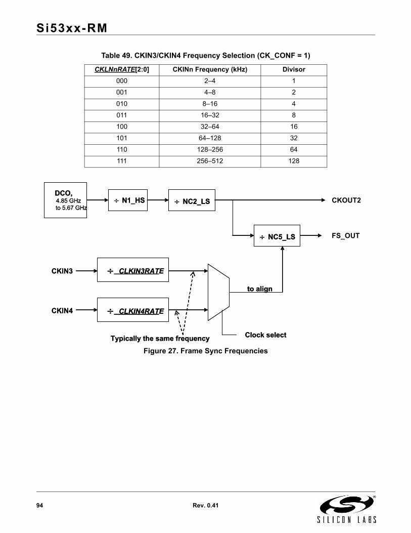
Si53xx-RM
94 Rev. 0.41
Figure 27. Frame Sync Frequencies
Table 49. CKIN3/CKIN4 Frequency Selection (CK_CONF = 1)
CKLNnRATE[2:0] CKINn Frequency (kHz) Divisor
000 2–4 1
001 4–8 2
010 8–16 4
011 16–32 8
100 32–64 16
101 64–128 32
110 128–256 64
111 256–512 128
CKIN3
CKIN4
CLKIN3RATE
Clock select
DCO,4.85 GHz to 5.67 GHz
CKOUT2 N1_HS NC2_LS
NC5_LS FS_OUT
CLKIN4RATE
to align
Typically the same frequency
CKIN3
CKIN4
CLKIN3RATE
Clock select
DCO,4.85 GHz to 5.67 GHz
N1_HS NC2_LS
NC5_LS
CLKIN4RATE
to align
Typically the same frequency
Si53xx-RM
Rev. 0.41 95
The NC5_LS divider uses CKOUT2 as its clock input to derive FS_OUT. The limits for the NC5_LS divider are
NC5_LS = [1, 2, 4, 6, …, 219]
fCKOUT2 < 710 MHz
Note that when in frame synchronization realignment mode, writes to NC5_LS are controlled by FPW_VALID. Seesection “7.8.4. FS_OUT Polarity and Pulse Width Control (Si5368)”.
Common NC5_LS divider settings on FS_OUT are shown in Table 50.
7.8.1. FSYNC Realignment (Si5368)
The FSYNC_ALIGN_PIN bit determines if the realignment will be pin-controlled via the FS_ALIGN pin or register-controlled via the FSYNC_ALIGN_REG register bit. The active CKIN3 or CKIN4 edge to be used is controlled viathe FSYNC_POL register bit.
The FSYNC realignment control can operate in level sensitive or one-shot mode as determined by theFSYNC_ALIGN_MODE register bit. The realignment control can be either the FS_ALIGN pin or theFSYNC_ALIGN_REG, as determined by the FSYNC_POL register bit.
Level Sensitive Mode: While realignment control is high, each active edge of the currently-active framesync input (CKIN_3 or CKIN_4) is used to control the NC5 output divider andtherefore the FS_OUT phase. Note that while the realignment control is active, itcannot be guaranteed that a fixed number of high-frequency clock (CKOUT_2)cycles exists between each FS_OUT cycle. See Figure 13, “Frame SynchronizationTiming in Level Sensitive Mode,” on page 32.
One Shot Mode: In the one-shot mode, after the FS_ALIGN pin or FSYNC_ALIGN_REG bit goesactive, the device will perform a one-time phase realignment on the next active edgeof the currently-active frame sync input. After the realignment, the FS_OUT willalways be a fixed number of CKOUT2 periods as determined by the NC5 setting asthe NC5 divider continuously divides down its CKOUT2 input. The one-shot mode ofoperation is helpful if the user wants a single realignment performed without havingto exactly control the timing of the FS_ALIGN or FSYNC_ALIGN_REG signals. SeeFigure 14, “Frame Synchronization Timing in One-shot Mode,” on page 32.
In either FSYNC alignment control mode, the resolution of the phase realignment is 1 clock cycle of CKOUT2. Ifthe realignment control is not active, the NC5 divider will continuously divide down its fCKOUT2 input. Thisguarantees a fixed number of high-frequency clock (CKOUT2) cycles between each FS_OUT cycle.
At power-up, the device automatically performs a realignment of FS_OUT using the currently active sync input.After this, as long as the PLL remains in lock and a realignment is not requested, FS_OUT will include a fixednumber of high-speed clock cycles, even if input clock switches are performed. If many clock switches areperformed in phase build-out mode, it is possible that the input sync to output sync phase relationship will shift dueto the accumulated residual phase transients of the phase build-out circuitry. The ALIGN_ERR[8:0] status registerreports the deviation of the input-to-output sync phase skew from the desired FSYNC_SKEW[16:0] value in units offCKOUT2 periods. A programmable threshold to trigger the ALIGN_INT alarm can be set via the ALIGN_THR[2:0]bits, whose settings are given in Table 51. If the sync alignment error exceeds the threshold in either the positive ornegative direction, the alarm becomes active. If it is then desired to reestablish the desired input-to-output sync
Table 50. Common NC5 Divider Settings
CKOUT2 Frequency (MHz) NC5 Divider Setting
2 kHz FS_OUT 8 kHz FS_OUT
19.44 9720 2430
77.76 38880 9720
155.52 77760 19440
622.08 311040 77760
Si53xx-RM
96 Rev. 0.41
phase relationship, a realignment can be performed. A realignment request may cause FS_OUT toinstantaneously shift its output edge location in order to align with the active input sync phase.
For cases where phase skew is required, see Section “7.7. Output Phase Adjust (Si5326, Si5368)” for more detailson controlling the sync input to sync output phase skew via the FSYNC_SKEW[16:0] bits. See Section “8.2. OutputClock Drivers” for information on the FS_OUT signal format, pulse width, and active logic level control.
7.8.2. FSYNC Skew Control
When CKIN3 and CKIN4 are configured as frame sync inputs (CK_CONFIG_REG = 1), phase skew of the syncinput active edge to FS_OUT active edge is controllable via the FSYNC_SKEW[16:0] register bits. Skew controlhas a resolution of 1/fCKOUT2 and a range of 131,071/fCKOUT2. The entered skew value must be less than theperiod of CKIN3, CKIN4, and FS_OUT.
The skew should not be changed more than once per FS_OUT period. If a FSYNC realignment is being made, theskew should not be changed until the realignment is complete. The skew value and the FS_OUT pulse widthshould not be changed within the same FS_OUT period.
Before writing the three bytes needed to specify a new FSYNC_SKEW[16:0] value, the user should set the registerbit FSKEW_VALID = 0. This causes the alignment state machine to keep using the previous FSYNC_SKEW[16:0]value, ignoring the new register values as they are being written. Once the new FSYNC_SKEW[16:0] value hasbeen completely written, the user should set FSKEW_VALID = 1 at which time the alignment state machine willread the new skew alignment value. Note that when the new FSYNC_SKEW[16:0] value is used, a phase step willoccur in FS_OUT.
7.8.3. Including FSYNC Inputs in Clock Selection (Si5368)
The frame sync inputs, CKIN3 and CKIN4, are both monitored for loss-of-signal (LOS3_INT and LOS4_INT)conditions. To include these LOS alarms in the input clock selection algorithm, set FSYNC_SWTCH_REG = 1. TheLOS3_INT is logically ORed with LOS1_INT and LOS4_INT is ORed with LOS2_INT as inputs to the clockselection state machine. If it is desired not to include these alarms in the clock selection algorithm, setFSYNC_SWTCH_REG = 0. The frequency offset (FOS) alarms for CKIN1 and CKIN2 can also be included in thestate machine decision making as described in Section “7.11. Alarms (Si5319, Si5325, Si5326, Si5367, Si5368)”;however, in frame sync mode (CK_CONFIG_REG = 1), the FOS alarms for CKIN3 and CKIN4 are ignored.
Table 51. Alignment Alarm Trigger Threshold
ALIGN_THR [2:0] Alarm Trigger Threshold (Units of TCKOUT2)
000 4
001 8
010 16
011 32
100 48
101 64
110 96
111 128
Si53xx-RM
Rev. 0.41 97
7.8.4. FS_OUT Polarity and Pulse Width Control (Si5368)
Additional output controls are available for FS_OUT. The active polarity of FS_OUT is set via the FS_OUT_POLregister bit and the active duty cycle is set via the FSYNC_PW[9:0] register. Pulse width settings have a resolutionof 1/fCKOUT2, and a 50% duty cycle setting is provided. Pulse width settings can range from 1 to (NC5-1) CKOUT2periods, providing the full range of pulse width possibilities for a given NC5 divider setting.
The FS_OUT pulse should not be changed more than once per FS_OUT period. If a FSYNC realignment is beingmade, the pulse width should not be changed until the realignment is complete. The FS_OUT pulse width and theskew value should not be changed within the same FS_OUT period.
Before writing a new value into FSYNC_PW[9:0], the user should set the register bit FPW_VALID = 0. This causesthe FS_OUT pulse width state machine to keep using the previous FSYNC_PW[9:0] value, ignoring the newregister values as they are being written. Once the new FSYNC_PW[9:0] value has been completely written, theuser should set FPW_VALID = 1, at which time the FS_OUT pulse width state machine will read the new pulsewidth value.
Writes to NC5_LS should be treated the same as writes to FSYNC_PW. Thus, all writes to NC5_LS should occuronly when FPW_VALID = 0. Any such writes will not take effect until FPW_VALID = 1.
Note that fCKOUT2 must be less than or equal to 710 MHz when CK_CONFIG_REG = 1; otherwise, the FS_OUTbuffer and NC5 divider must be disabled.
7.8.5. Using FS_OUT as a Fifth Output Clock (Si5368)
In applications where the frame synchronization functionality is not needed (CK_CONFIG_REG = 0), FS_OUT canbe used as a fifth clock output. In this case, no realignment requests should be made to the NC5 divider (holdFS_ALIGN = 0 and FSYNC_ALIGN_REG = 0). Output pulse width and polarity controls for FS_OUT are stillavailable as described above. The 50% duty cycle setting would be used to generate a typical balanced outputclock.
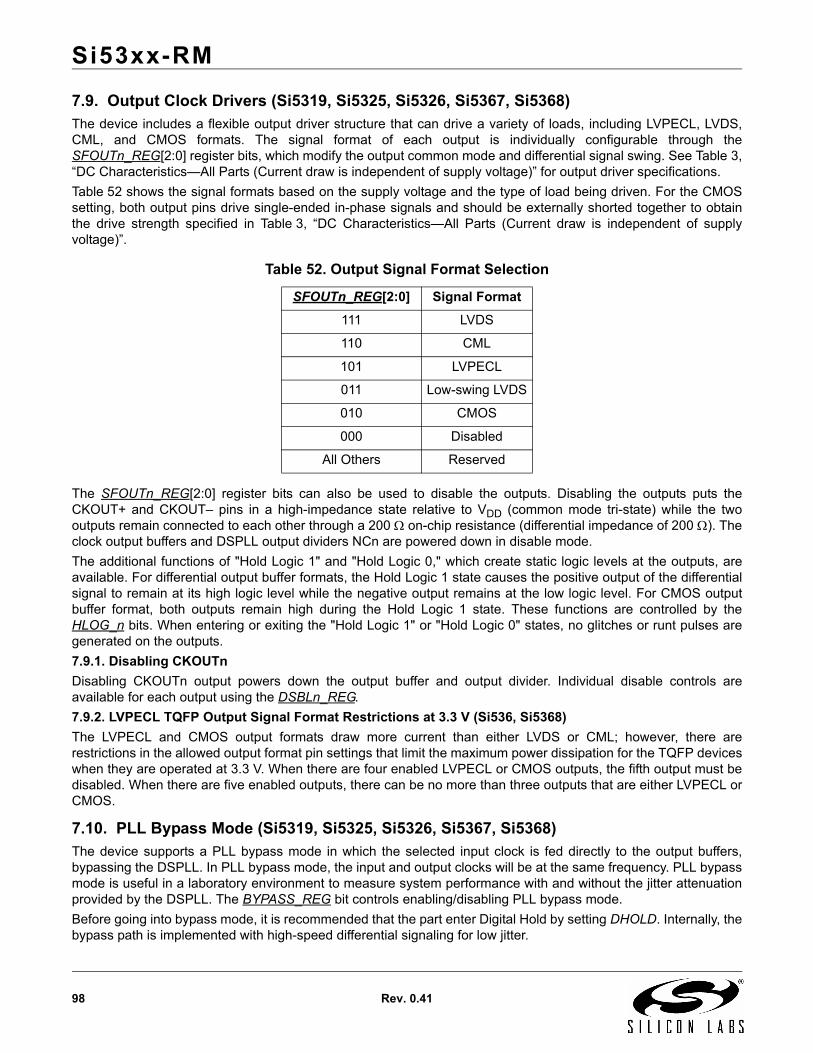
Si53xx-RM
98 Rev. 0.41
7.9. Output Clock Drivers (Si5319, Si5325, Si5326, Si5367, Si5368)The device includes a flexible output driver structure that can drive a variety of loads, including LVPECL, LVDS,CML, and CMOS formats. The signal format of each output is individually configurable through theSFOUTn_REG[2:0] register bits, which modify the output common mode and differential signal swing. See Table 3,“DC Characteristics—All Parts (Current draw is independent of supply voltage)” for output driver specifications.
Table 52 shows the signal formats based on the supply voltage and the type of load being driven. For the CMOSsetting, both output pins drive single-ended in-phase signals and should be externally shorted together to obtainthe drive strength specified in Table 3, “DC Characteristics—All Parts (Current draw is independent of supplyvoltage)”.
The SFOUTn_REG[2:0] register bits can also be used to disable the outputs. Disabling the outputs puts theCKOUT+ and CKOUT– pins in a high-impedance state relative to VDD (common mode tri-state) while the twooutputs remain connected to each other through a 200 on-chip resistance (differential impedance of 200 ). Theclock output buffers and DSPLL output dividers NCn are powered down in disable mode.
The additional functions of "Hold Logic 1" and "Hold Logic 0," which create static logic levels at the outputs, areavailable. For differential output buffer formats, the Hold Logic 1 state causes the positive output of the differentialsignal to remain at its high logic level while the negative output remains at the low logic level. For CMOS outputbuffer format, both outputs remain high during the Hold Logic 1 state. These functions are controlled by theHLOG_n bits. When entering or exiting the "Hold Logic 1" or "Hold Logic 0" states, no glitches or runt pulses aregenerated on the outputs.
7.9.1. Disabling CKOUTn
Disabling CKOUTn output powers down the output buffer and output divider. Individual disable controls areavailable for each output using the DSBLn_REG.
7.9.2. LVPECL TQFP Output Signal Format Restrictions at 3.3 V (Si536, Si5368)
The LVPECL and CMOS output formats draw more current than either LVDS or CML; however, there arerestrictions in the allowed output format pin settings that limit the maximum power dissipation for the TQFP deviceswhen they are operated at 3.3 V. When there are four enabled LVPECL or CMOS outputs, the fifth output must bedisabled. When there are five enabled outputs, there can be no more than three outputs that are either LVPECL orCMOS.
7.10. PLL Bypass Mode (Si5319, Si5325, Si5326, Si5367, Si5368)The device supports a PLL bypass mode in which the selected input clock is fed directly to the output buffers,bypassing the DSPLL. In PLL bypass mode, the input and output clocks will be at the same frequency. PLL bypassmode is useful in a laboratory environment to measure system performance with and without the jitter attenuationprovided by the DSPLL. The BYPASS_REG bit controls enabling/disabling PLL bypass mode.
Before going into bypass mode, it is recommended that the part enter Digital Hold by setting DHOLD. Internally, thebypass path is implemented with high-speed differential signaling for low jitter.
Table 52. Output Signal Format Selection
SFOUTn_REG[2:0] Signal Format
111 LVDS
110 CML
101 LVPECL
011 Low-swing LVDS
010 CMOS
000 Disabled
All Others Reserved
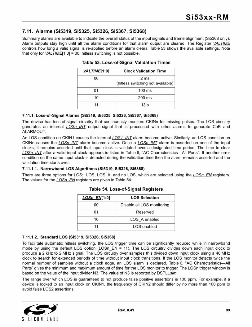
Si53xx-RM
Rev. 0.41 99
7.11. Alarms (Si5319, Si5325, Si5326, Si5367, Si5368)Summary alarms are available to indicate the overall status of the input signals and frame alignment (Si5368 only).Alarm outputs stay high until all the alarm conditions for that alarm output are cleared. The Register VALTIMEcontrols how long a valid signal is re-applied before an alarm clears. Table 53 shows the available settings. Notethat only for VALTIME[1:0] = 00, hitless switching is not possible.
7.11.1. Loss-of-Signal Alarms (Si5319, Si5325, Si5326, Si5367, Si5368)
The device has loss-of-signal circuitry that continuously monitors CKINn for missing pulses. The LOS circuitrygenerates an internal LOSn_INT output signal that is processed with other alarms to generate CnB andALARMOUT.
An LOS condition on CKIN1 causes the internal LOS1_INT alarm become active. Similarly, an LOS condition onCKINn causes the LOSn_INT alarm become active. Once a LOSn_INT alarm is asserted on one of the inputclocks, it remains asserted until that input clock is validated over a designated time period. The time to clearLOSn_INT after a valid input clock appears is listed in Table 6, “AC Characteristics—All Parts”. If another errorcondition on the same input clock is detected during the validation time then the alarm remains asserted and thevalidation time starts over.
7.11.1.1. Narrowband LOS Algorithms (Si5319, Si5326, Si5368)
There are three options for LOS: LOS, LOS_A, and no LOS, which are selected using the LOSn_EN registers.The values for the LOSn_EN registers are given in Table 54.
7.11.1.2. Standard LOS (Si5319, Si5326, Si5368)
To facilitate automatic hitless switching, the LOS trigger time can be significantly reduced while in narrowbandmode by using the default LOS option (LOSn_EN = 11). The LOS circuitry divides down each input clock toproduce a 2 kHz to 2 MHz signal. The LOS circuitry over samples this divided down input clock using a 40 MHzclock to search for extended periods of time without input clock transitions. If the LOS monitor detects twice thenormal number of samples without a clock edge, an LOS alarm is declared. Table 6, “AC Characteristics—AllParts” gives the minimum and maximum amount of time for the LOS monitor to trigger. The LOSn trigger window isbased on the value of the input divider N3. The value of N3 is reported by DSPLLsim.
The range over which LOS is guaranteed to not produce false positive assertions is 100 ppm. For example, if adevice is locked to an input clock on CKIN1, the frequency of CKIN2 should differ by no more than 100 ppm toavoid false LOS2 assertions.
Table 53. Loss-of-Signal Validation Times
VALTIME[1:0] Clock Validation Time
00 2 ms (hitless switching not available)
01 100 ms
10 200 ms
11 13 s
Table 54. Loss-of-Signal Registers
LOSn_EN[1:0] LOS Selection
00 Disable all LOS monitoring
01 Reserved
10 LOS_A enabled
11 LOS enabled
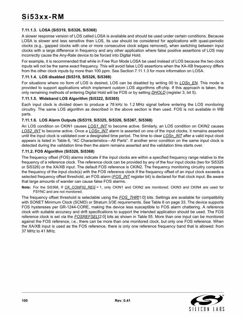
Si53xx-RM
100 Rev. 0.41
7.11.1.3. LOSA (Si5319, Si5326, Si5368)
A slower response version of LOS called LOSA is available and should be used under certain conditions. BecauseLOSA is slower and less sensitive than LOS, its use should be considered for applications with quasi-periodicclocks (e.g., gapped clocks with one or more consecutive clock edges removed), when switching between inputclocks with a large difference in frequency and any other application where false positive assertions of LOS mayincorrectly cause the Any-Rate device to be forced into Digital Hold.
For example, it is recommended that while in Free Run Mode LOSA be used instead of LOS because the two clockinputs will not be the same exact frequency. This will avoid false LOS assertions when the XA-XB frequency differsfrom the other clock inputs by more than 100 ppm. See Section 7.11.1.3 for more information on LOSA.
7.11.1.4. LOS disabled (Si5319, Si5326, Si5368)
For situations where no form of LOS is desired, LOS can be disabled by writing 00 to LOSn_EN. This mode isprovided to support applications which implement custom LOS algorithms off-chip. If this approach is taken, theonly remaining methods of entering Digital Hold will be FOS or by setting DHOLD (register 3, bit 5).
7.11.1.5. Wideband LOS Algorithm (Si5322, Si5365)
Each input clock is divided down to produce a 78 kHz to 1.2 MHz signal before entering the LOS monitoringcircuitry. The same LOS algorithm as described in the above section is then used. FOS is not available in WBparts.
7.11.1.6. LOS Alarm Outputs (Si5319, Si5325, Si5326, Si5367, Si5368)
An LOS condition on CKIN1 causes LOS1_INT to become active. Similarly, an LOS condition on CKIN2 causesLOS2_INT to become active. Once a LOSn_INT alarm is asserted on one of the input clocks, it remains asserteduntil the input clock is validated over a designated time period. The time to clear LOSn_INT after a valid input clockappears is listed in Table 6, “AC Characteristics—All Parts”. If another error condition on the same input clock isdetected during the validation time then the alarm remains asserted and the validation time starts over.
7.11.2. FOS Algorithm (Si5326, Si5368)
The frequency offset (FOS) alarms indicate if the input clocks are within a specified frequency range relative to thefrequency of a reference clock. The reference clock can be provided by any of the four input clocks (two for Si5325or Si5326) or the XA/XB input. The default FOS reference is CKIN2. The frequency monitoring circuitry comparesthe frequency of the input clock(s) with the FOS reference clock If the frequency offset of an input clock exceeds aselected frequency offset threshold, an FOS alarm (FOS_INT register bit) is declared for that clock input. Be awarethat large amounts of wander can cause false FOS alarms.
Note: For the Si5368, If CK_CONFIG_REG = 1, only CKIN1 and CKIN2 are monitored; CKIN3 and CKIN4 are used forFSYNC and are not monitored.
The frequency offset threshold is selectable using the FOS_THR[1:0] bits. Settings are available for compatibilitywith SONET Minimum Clock (SCMD) or Stratum 3/3E requirements. See Table 6 on page 33. The device supportsFOS hystereses per GR-1244-CORE, making the device less susceptible to FOS alarm chattering. A referenceclock with suitable accuracy and drift specifications to support the intended application should be used. The FOSreference clock is set via the FOSREFSEL[2:0] bits as shown in Table 55. More than one input can be monitoredagainst the FOS reference, i.e., there can be more than one monitored clock, but only one FOS reference. Whenthe XA/XB input is used as the FOS reference, there is only one reference frequency band that is allowed: from37 MHz to 41 MHz.
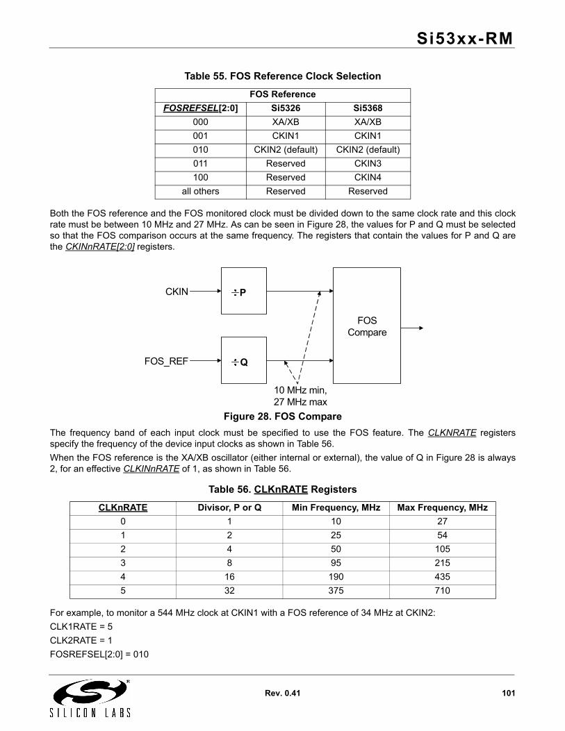
Si53xx-RM
Rev. 0.41 101
Both the FOS reference and the FOS monitored clock must be divided down to the same clock rate and this clockrate must be between 10 MHz and 27 MHz. As can be seen in Figure 28, the values for P and Q must be selectedso that the FOS comparison occurs at the same frequency. The registers that contain the values for P and Q arethe CKINnRATE[2:0] registers.
Figure 28. FOS Compare
The frequency band of each input clock must be specified to use the FOS feature. The CLKNRATE registersspecify the frequency of the device input clocks as shown in Table 56.
When the FOS reference is the XA/XB oscillator (either internal or external), the value of Q in Figure 28 is always2, for an effective CLKINnRATE of 1, as shown in Table 56.
For example, to monitor a 544 MHz clock at CKIN1 with a FOS reference of 34 MHz at CKIN2:
CLK1RATE = 5
CLK2RATE = 1
FOSREFSEL[2:0] = 010
Table 55. FOS Reference Clock Selection
FOS Reference
FOSREFSEL[2:0] Si5326 Si5368
000 XA/XB XA/XB
001 CKIN1 CKIN1
010 CKIN2 (default) CKIN2 (default)
011 Reserved CKIN3
100 Reserved CKIN4
all others Reserved Reserved
Table 56. CLKnRATE Registers
CLKnRATE Divisor, P or Q Min Frequency, MHz Max Frequency, MHz
0 1 10 27
1 2 25 54
2 4 50 105
3 8 95 215
4 16 190 435
5 32 375 710
CKIN
FOS_REF
P
Q
FOS Compare
10 MHz min,27 MHz max
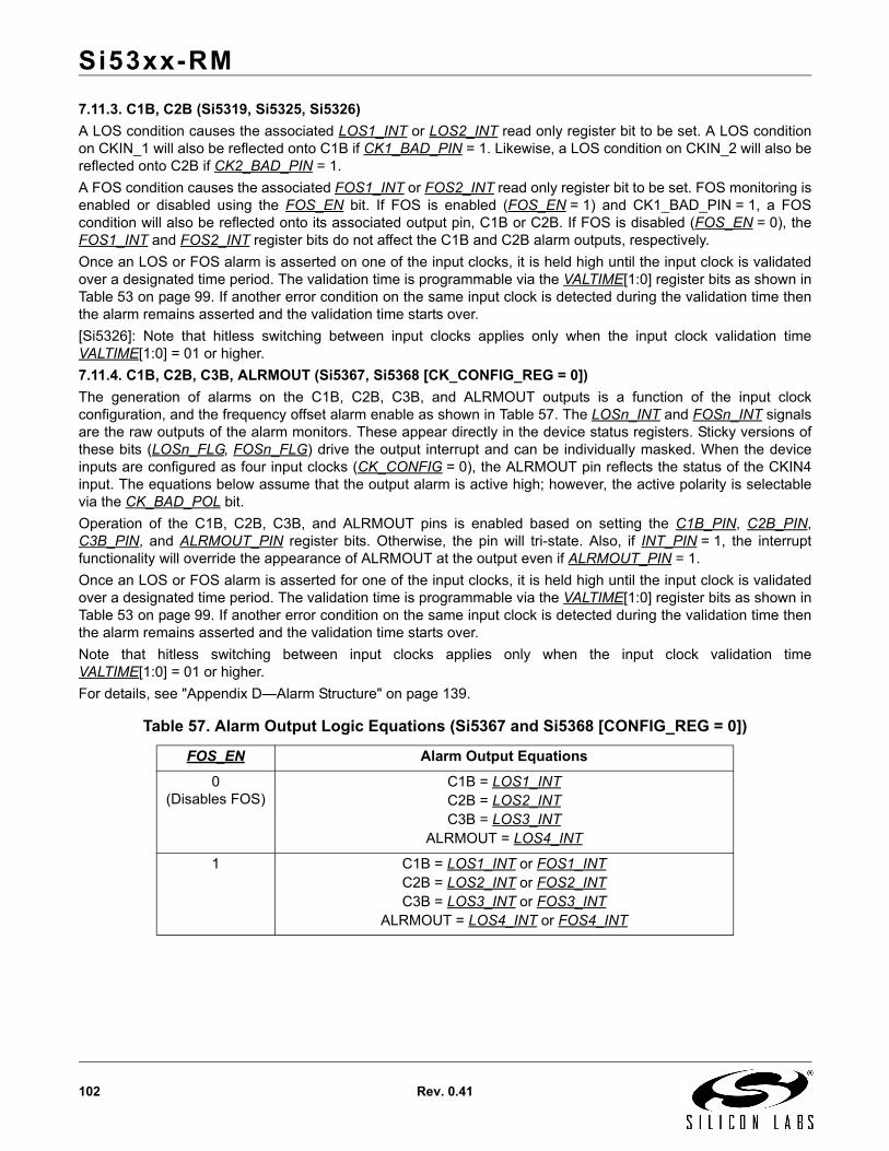
Si53xx-RM
102 Rev. 0.41
7.11.3. C1B, C2B (Si5319, Si5325, Si5326)
A LOS condition causes the associated LOS1_INT or LOS2_INT read only register bit to be set. A LOS conditionon CKIN_1 will also be reflected onto C1B if CK1_BAD_PIN = 1. Likewise, a LOS condition on CKIN_2 will also bereflected onto C2B if CK2_BAD_PIN = 1.
A FOS condition causes the associated FOS1_INT or FOS2_INT read only register bit to be set. FOS monitoring isenabled or disabled using the FOS_EN bit. If FOS is enabled (FOS_EN = 1) and CK1_BAD_PIN = 1, a FOScondition will also be reflected onto its associated output pin, C1B or C2B. If FOS is disabled (FOS_EN = 0), theFOS1_INT and FOS2_INT register bits do not affect the C1B and C2B alarm outputs, respectively.
Once an LOS or FOS alarm is asserted on one of the input clocks, it is held high until the input clock is validatedover a designated time period. The validation time is programmable via the VALTIME[1:0] register bits as shown inTable 53 on page 99. If another error condition on the same input clock is detected during the validation time thenthe alarm remains asserted and the validation time starts over.
[Si5326]: Note that hitless switching between input clocks applies only when the input clock validation timeVALTIME[1:0] = 01 or higher.
7.11.4. C1B, C2B, C3B, ALRMOUT (Si5367, Si5368 [CK_CONFIG_REG = 0])
The generation of alarms on the C1B, C2B, C3B, and ALRMOUT outputs is a function of the input clockconfiguration, and the frequency offset alarm enable as shown in Table 57. The LOSn_INT and FOSn_INT signalsare the raw outputs of the alarm monitors. These appear directly in the device status registers. Sticky versions ofthese bits (LOSn_FLG, FOSn_FLG) drive the output interrupt and can be individually masked. When the deviceinputs are configured as four input clocks (CK_CONFIG = 0), the ALRMOUT pin reflects the status of the CKIN4input. The equations below assume that the output alarm is active high; however, the active polarity is selectablevia the CK_BAD_POL bit.
Operation of the C1B, C2B, C3B, and ALRMOUT pins is enabled based on setting the C1B_PIN, C2B_PIN,C3B_PIN, and ALRMOUT_PIN register bits. Otherwise, the pin will tri-state. Also, if INT_PIN = 1, the interruptfunctionality will override the appearance of ALRMOUT at the output even if ALRMOUT_PIN = 1.
Once an LOS or FOS alarm is asserted for one of the input clocks, it is held high until the input clock is validatedover a designated time period. The validation time is programmable via the VALTIME[1:0] register bits as shown inTable 53 on page 99. If another error condition on the same input clock is detected during the validation time thenthe alarm remains asserted and the validation time starts over.
Note that hitless switching between input clocks applies only when the input clock validation timeVALTIME[1:0] = 01 or higher.
For details, see "Appendix D—Alarm Structure" on page 139.
Table 57. Alarm Output Logic Equations (Si5367 and Si5368 [CONFIG_REG = 0])
FOS_EN Alarm Output Equations
0(Disables FOS)
C1B = LOS1_INTC2B = LOS2_INTC3B = LOS3_INT
ALRMOUT = LOS4_INT
1 C1B = LOS1_INT or FOS1_INTC2B = LOS2_INT or FOS2_INTC3B = LOS3_INT or FOS3_INT
ALRMOUT = LOS4_INT or FOS4_INT
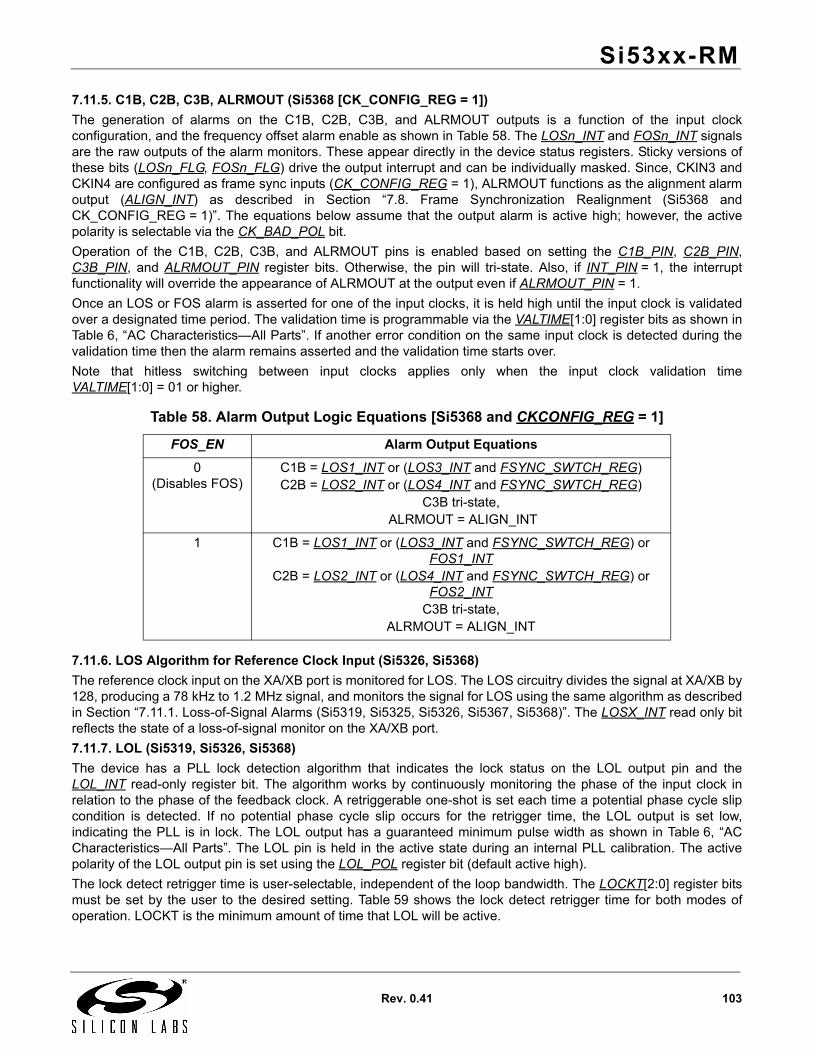
Si53xx-RM
Rev. 0.41 103
7.11.5. C1B, C2B, C3B, ALRMOUT (Si5368 [CK_CONFIG_REG = 1])
The generation of alarms on the C1B, C2B, C3B, and ALRMOUT outputs is a function of the input clockconfiguration, and the frequency offset alarm enable as shown in Table 58. The LOSn_INT and FOSn_INT signalsare the raw outputs of the alarm monitors. These appear directly in the device status registers. Sticky versions ofthese bits (LOSn_FLG, FOSn_FLG) drive the output interrupt and can be individually masked. Since, CKIN3 andCKIN4 are configured as frame sync inputs (CK_CONFIG_REG = 1), ALRMOUT functions as the alignment alarmoutput (ALIGN_INT) as described in Section “7.8. Frame Synchronization Realignment (Si5368 andCK_CONFIG_REG = 1)”. The equations below assume that the output alarm is active high; however, the activepolarity is selectable via the CK_BAD_POL bit.
Operation of the C1B, C2B, C3B, and ALRMOUT pins is enabled based on setting the C1B_PIN, C2B_PIN,C3B_PIN, and ALRMOUT_PIN register bits. Otherwise, the pin will tri-state. Also, if INT_PIN = 1, the interruptfunctionality will override the appearance of ALRMOUT at the output even if ALRMOUT_PIN = 1.
Once an LOS or FOS alarm is asserted for one of the input clocks, it is held high until the input clock is validatedover a designated time period. The validation time is programmable via the VALTIME[1:0] register bits as shown inTable 6, “AC Characteristics—All Parts”. If another error condition on the same input clock is detected during thevalidation time then the alarm remains asserted and the validation time starts over.
Note that hitless switching between input clocks applies only when the input clock validation timeVALTIME[1:0] = 01 or higher.
7.11.6. LOS Algorithm for Reference Clock Input (Si5326, Si5368)
The reference clock input on the XA/XB port is monitored for LOS. The LOS circuitry divides the signal at XA/XB by128, producing a 78 kHz to 1.2 MHz signal, and monitors the signal for LOS using the same algorithm as describedin Section “7.11.1. Loss-of-Signal Alarms (Si5319, Si5325, Si5326, Si5367, Si5368)”. The LOSX_INT read only bitreflects the state of a loss-of-signal monitor on the XA/XB port.
7.11.7. LOL (Si5319, Si5326, Si5368)
The device has a PLL lock detection algorithm that indicates the lock status on the LOL output pin and theLOL_INT read-only register bit. The algorithm works by continuously monitoring the phase of the input clock inrelation to the phase of the feedback clock. A retriggerable one-shot is set each time a potential phase cycle slipcondition is detected. If no potential phase cycle slip occurs for the retrigger time, the LOL output is set low,indicating the PLL is in lock. The LOL output has a guaranteed minimum pulse width as shown in Table 6, “ACCharacteristics—All Parts”. The LOL pin is held in the active state during an internal PLL calibration. The activepolarity of the LOL output pin is set using the LOL_POL register bit (default active high).
The lock detect retrigger time is user-selectable, independent of the loop bandwidth. The LOCKT[2:0] register bitsmust be set by the user to the desired setting. Table 59 shows the lock detect retrigger time for both modes ofoperation. LOCKT is the minimum amount of time that LOL will be active.
Table 58. Alarm Output Logic Equations [Si5368 and CKCONFIG_REG = 1]
FOS_EN Alarm Output Equations
0(Disables FOS)
C1B = LOS1_INT or (LOS3_INT and FSYNC_SWTCH_REG)C2B = LOS2_INT or (LOS4_INT and FSYNC_SWTCH_REG)
C3B tri-state, ALRMOUT = ALIGN_INT
1 C1B = LOS1_INT or (LOS3_INT and FSYNC_SWTCH_REG) or FOS1_INT
C2B = LOS2_INT or (LOS4_INT and FSYNC_SWTCH_REG) or FOS2_INT
C3B tri-state, ALRMOUT = ALIGN_INT
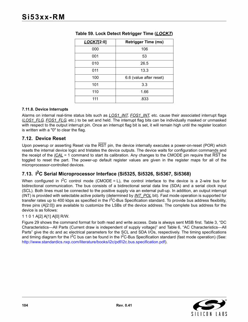
Si53xx-RM
104 Rev. 0.41
7.11.8. Device Interrupts
Alarms on internal real-time status bits such as LOS1_INT, FOS1_INT, etc. cause their associated interrupt flags(LOS1_FLG, FOS1_FLG, etc.) to be set and held. The interrupt flag bits can be individually masked or unmaskedwith respect to the output interrupt pin. Once an interrupt flag bit is set, it will remain high until the register locationis written with a "0" to clear the flag.
7.12. Device ResetUpon powerup or asserting Reset via the RST pin, the device internally executes a power-on-reset (POR) whichresets the internal device logic and tristates the device outputs. The device waits for configuration commands andthe receipt of the ICAL = 1 command to start its calibration. Any changes to the CMODE pin require that RST betoggled to reset the part. The power-up default register values are given in the register maps for all of themicroprocessor-controlled devices.
7.13. I2C Serial Microprocessor Interface (Si5325, Si5326, Si5367, Si5368)When configured in I2C control mode (CMODE = L), the control interface to the device is a 2-wire bus forbidirectional communication. The bus consists of a bidirectional serial data line (SDA) and a serial clock input(SCL). Both lines must be connected to the positive supply via an external pull-up. In addition, an output interrupt(INT) is provided with selectable active polarity (determined by INT_POL bit). Fast mode operation is supported fortransfer rates up to 400 kbps as specified in the I2C-Bus Specification standard. To provide bus address flexibility,three pins (A[2:0]) are available to customize the LSBs of the device address. The complete bus address for thedevice is as follows:
1 1 0 1 A[2] A[1] A[0] R/W.
Figure 29 shows the command format for both read and write access. Data is always sent MSB first. Table 3, “DCCharacteristics—All Parts (Current draw is independent of supply voltage)” and Table 6, “AC Characteristics—AllParts” give the dc and ac electrical parameters for the SCL and SDA I/Os, respectively. The timing specificationsand timing diagram for the I2C bus can be found in the I2C-Bus Specification standard (fast mode operation) (See:http://www.standardics.nxp.com/literature/books/i2c/pdf/i2c.bus.specification.pdf).
Table 59. Lock Detect Retrigger Time (LOCKT)
LOCKT[2:0] Retrigger Time (ms)
000 106
001 53
010 26.5
011 13.3
100 6.6 (value after reset)
101 3.3
110 1.66
111 .833
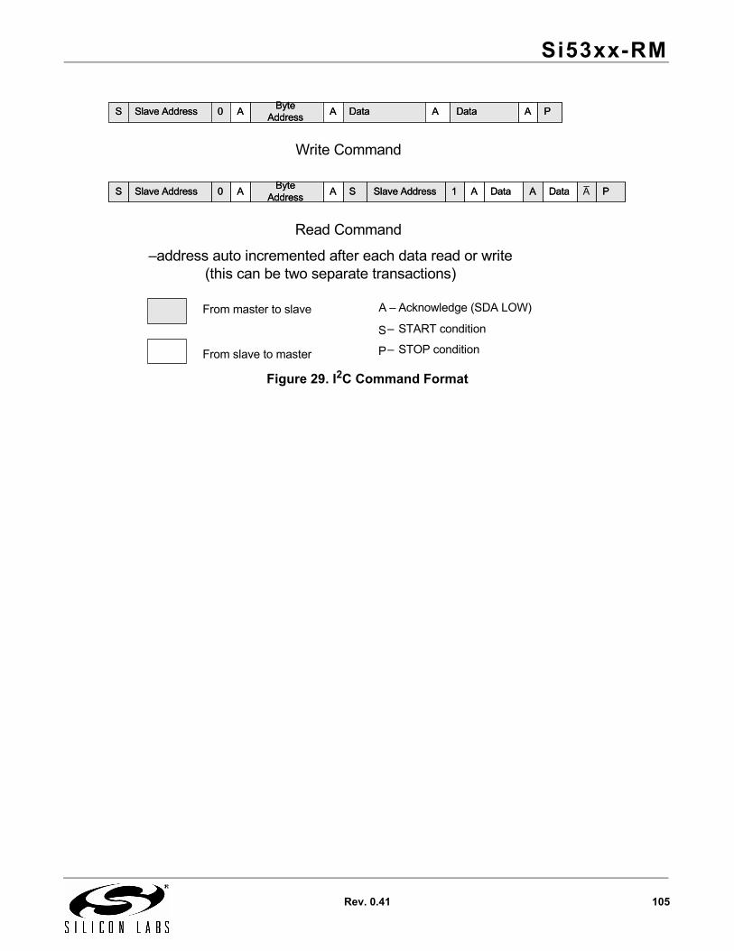
Si53xx-RM
Rev. 0.41 105
Figure 29. I2C Command Format
A Data A Data PA1Slave AddressSAByte
AddressA0Slave AddressS A Data A Data P1Slave AddressSA
Byte Address
A0Slave AddressS
From master to slave
From slave to master
A – Acknowledge (SDA LOW)
S – START condition
P– STOP condition
Write Command
Read Command
–address auto incremented after each data read or write (this can be two separate transactions)
PADataADataAByte
AddressA0Slave AddressS PADataADataA
Byte Address
A0Slave AddressS
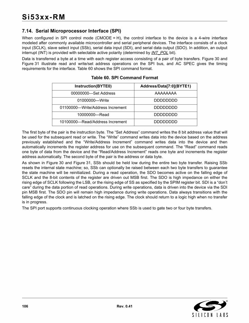
Si53xx-RM
106 Rev. 0.41
7.14. Serial Microprocessor Interface (SPI)When configured in SPI control mode (CMODE = H), the control interface to the device is a 4-wire interfacemodeled after commonly available microcontroller and serial peripheral devices. The interface consists of a clockinput (SCLK), slave select input (SSb), serial data input (SDI), and serial data output (SDO). In addition, an outputinterrupt (INT) is provided with selectable active polarity (determined by INT_POL bit).
Data is transferred a byte at a time with each register access consisting of a pair of byte transfers. Figure 30 andFigure 31 illustrate read and write/set address operations on the SPI bus, and AC SPEC gives the timingrequirements for the interface. Table 60 shows the SPI command format.
The first byte of the pair is the instruction byte. The “Set Address” command writes the 8 bit address value that willbe used for the subsequent read or write. The “Write” command writes data into the device based on the addresspreviously established and the “Write/Address Increment” command writes data into the device and thenautomatically increments the register address for use on the subsequent command. The “Read” command readsone byte of data from the device and the “Read/Address Increment” reads one byte and increments the registeraddress automatically. The second byte of the pair is the address or data byte.
As shown in Figure 30 and Figure 31, SSb should be held low during the entire two byte transfer. Raising SSbresets the internal state machine; so, SSb can optionally be raised between each two byte transfers to guaranteethe state machine will be reinitialized. During a read operation, the SDO becomes active on the falling edge ofSCLK and the 8-bit contents of the register are driven out MSB first. The SDO is high impedance on either therising edge of SCLK following the LSB, or the rising edge of SS as specified by the SPIM register bit. SDI is a “don’tcare” during the data portion of read operations. During write operations, data is driven into the device via the SDIpin MSB first. The SDO pin will remain high impedance during write operations. Data always transitions with thefalling edge of the clock and is latched on the rising edge. The clock should return to a logic high when no transferis in progress.
The SPI port supports continuous clocking operation where SSb is used to gate two or four byte transfers.
Table 60. SPI Command Format
Instruction(BYTE0) Address/Data[7:0](BYTE1)
00000000—Set Address AAAAAAAA
01000000—Write DDDDDDDD
01100000—Write/Address Increment DDDDDDDD
10000000—Read DDDDDDDD
10100000—Read/Address Increment DDDDDDDD
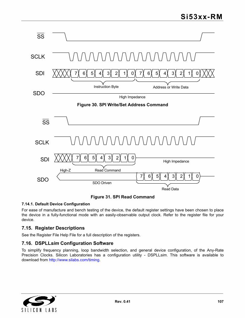
Si53xx-RM
Rev. 0.41 107
Figure 30. SPI Write/Set Address Command
Figure 31. SPI Read Command
7.14.1. Default Device Configuration
For ease of manufacture and bench testing of the device, the default register settings have been chosen to placethe device in a fully-functional mode with an easily-observable output clock. Refer to the register file for yourdevice.
7.15. Register DescriptionsSee the Register File Help File for a full description of the registers.
7.16. DSPLLsim Configuration SoftwareTo simplify frequency planning, loop bandwidth selection, and general device configuration, of the Any-RatePrecision Clocks. Silicon Laboratories has a configuration utility - DSPLLsim. This software is available todownload from http://www.silabs.com/timing.
SS
SCLK
SDI
SDO
7 6 5 4 3 2 1 0 7 6 5 4 3 2 1 0
High Impedance
Instruction Byte Address or Write Data
SS
SCLK
SDI
SDO
7 6 5 4 3 2 1
7 6 5 4 3 2 1 0
SDO Driven
High Impedance0
Read Command
Read Data
High-Z
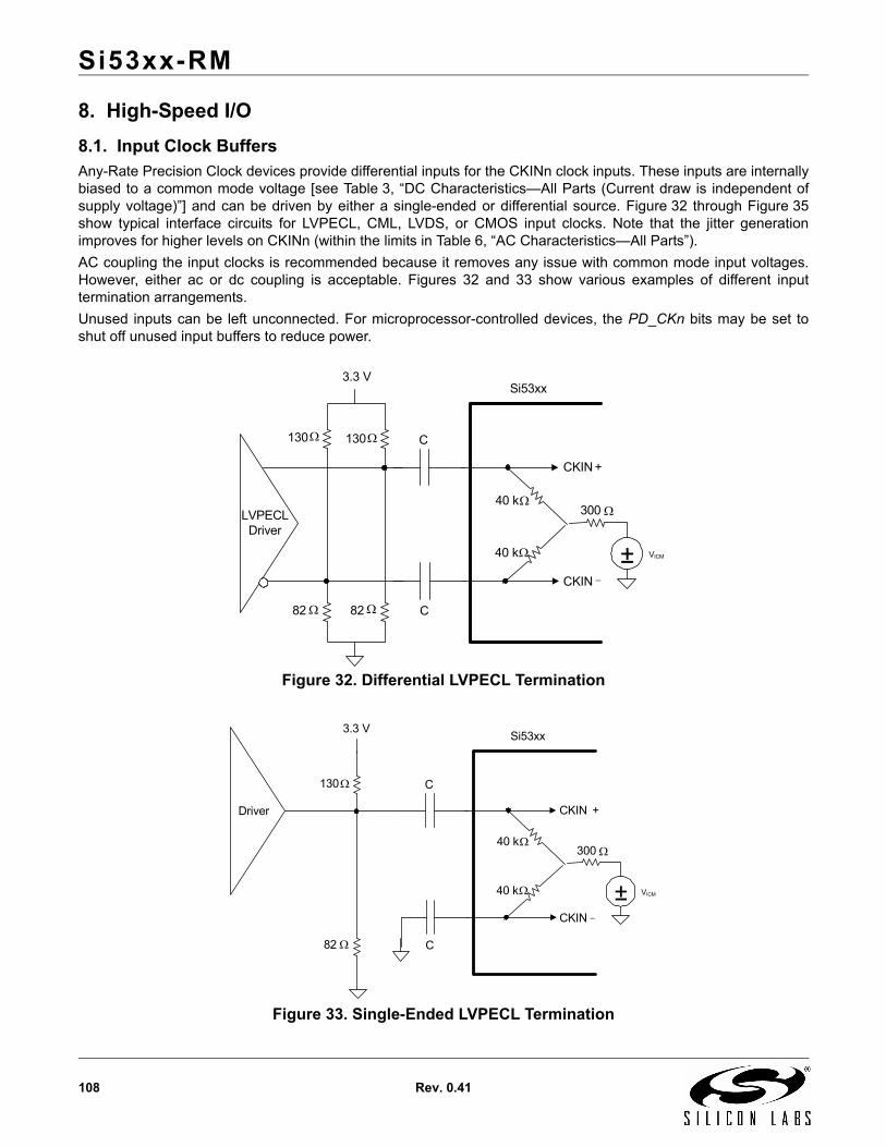
Si53xx-RM
108 Rev. 0.41
8. High-Speed I/O
8.1. Input Clock BuffersAny-Rate Precision Clock devices provide differential inputs for the CKINn clock inputs. These inputs are internallybiased to a common mode voltage [see Table 3, “DC Characteristics—All Parts (Current draw is independent ofsupply voltage)”] and can be driven by either a single-ended or differential source. Figure 32 through Figure 35show typical interface circuits for LVPECL, CML, LVDS, or CMOS input clocks. Note that the jitter generationimproves for higher levels on CKINn (within the limits in Table 6, “AC Characteristics—All Parts”).
AC coupling the input clocks is recommended because it removes any issue with common mode input voltages.However, either ac or dc coupling is acceptable. Figures 32 and 33 show various examples of different inputtermination arrangements.
Unused inputs can be left unconnected. For microprocessor-controlled devices, the PD_CKn bits may be set toshut off unused input buffers to reduce power.
Figure 32. Differential LVPECL Termination
Figure 33. Single-Ended LVPECL Termination
40 k
C
C
±CKIN _
CKIN +
VICM
300
130 130
3.3 V
8282
Si53xx
LVPECLDriver
40 k
40 k
C
C
±CKIN _
CKIN +
VICM
300
130
3.3 V
82
Si53xx
Driver
40 k
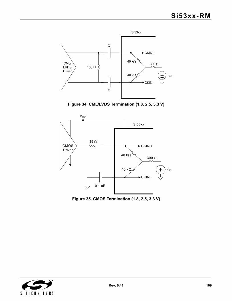
Si53xx-RM
Rev. 0.41 109
Figure 34. CML/LVDS Termination (1.8, 2.5, 3.3 V)
Figure 35. CMOS Termination (1.8, 2.5, 3.3 V)
40 k
C
C
±CKIN _
CKIN +
VICM
300100
Si53xx
CML/LVDSDriver
40 k
40 k
0.1 uF
±CKIN _
CKIN +
300
Si53xx
CMOSDriver
40 k VICM
39
VDD
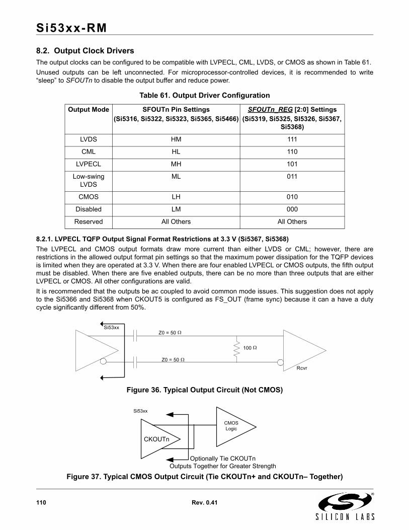
Si53xx-RM
110 Rev. 0.41
8.2. Output Clock DriversThe output clocks can be configured to be compatible with LVPECL, CML, LVDS, or CMOS as shown in Table 61.
Unused outputs can be left unconnected. For microprocessor-controlled devices, it is recommended to write“sleep” to SFOUTn to disable the output buffer and reduce power.
8.2.1. LVPECL TQFP Output Signal Format Restrictions at 3.3 V (Si5367, Si5368)
The LVPECL and CMOS output formats draw more current than either LVDS or CML; however, there arerestrictions in the allowed output format pin settings so that the maximum power dissipation for the TQFP devicesis limited when they are operated at 3.3 V. When there are four enabled LVPECL or CMOS outputs, the fifth outputmust be disabled. When there are five enabled outputs, there can be no more than three outputs that are eitherLVPECL or CMOS. All other configurations are valid.
It is recommended that the outputs be ac coupled to avoid common mode issues. This suggestion does not applyto the Si5366 and Si5368 when CKOUT5 is configured as FS_OUT (frame sync) because it can a have a dutycycle significantly different from 50%.
Figure 36. Typical Output Circuit (Not CMOS)
Figure 37. Typical CMOS Output Circuit (Tie CKOUTn+ and CKOUTn– Together)
Table 61. Output Driver Configuration
Output Mode SFOUTn Pin Settings
(Si5316, Si5322, Si5323, Si5365, Si5466)
SFOUTn_REG [2:0] Settings
(Si5319, Si5325, SI5326, Si5367, Si5368)
LVDS HM 111
CML HL 110
LVPECL MH 101
Low-swing LVDS
ML 011
CMOS LH 010
Disabled LM 000
Reserved All Others All Others
Si53xx
Rcvr
100
Z0 = 50
Z0 = 50
Si53xx
CMOSLogic
CKOUTn
Optionally Tie CKOUTnOutputs Together for Greater Strength
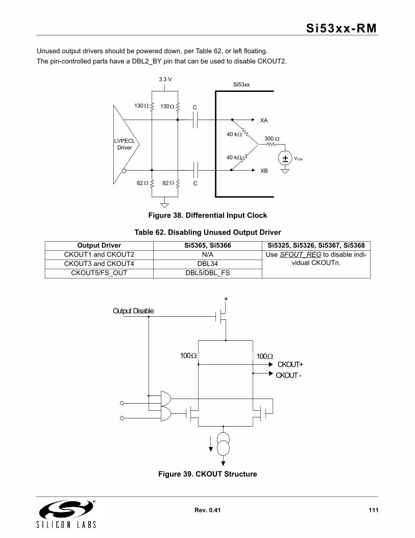
Si53xx-RM
Rev. 0.41 111
Unused output drivers should be powered down, per Table 62, or left floating.
The pin-controlled parts have a DBL2_BY pin that can be used to disable CKOUT2.
Figure 38. Differential Input Clock
Figure 39. CKOUT Structure
Table 62. Disabling Unused Output Driver
Output Driver Si5365, Si5366 Si5325, Si5326, Si5367, Si5368CKOUT1 and CKOUT2 N/A Use SFOUT_REG to disable indi-
vidual CKOUTn.CKOUT3 and CKOUT4 DBL34CKOUT5/FS_OUT DBL5/DBL_FS
40 k
C
C
±XB
XA
VICM
300
130 130
3.3 V
8282
Si53xx
LVPECLDriver
40 k
Output Disable
100 100
+
CKOUT+
CKOUT -
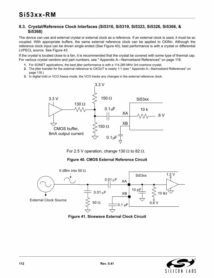
Si53xx-RM
112 Rev. 0.41
8.3. Crystal/Reference Clock Interfaces (Si5316, Si5319, Si5323, Si5326, Si5366, & Si5368)
The device can use and external crystal or external clock as a reference. If an external clock is used, it must be accoupled. With appropriate buffers, the same external reference clock can be applied to CKINn. Although thereference clock input can be driven single ended (See Figure 40), best performance is with a crystal or differentialLVPECL source. See Figure 43.
If the crystal is located close to a fan, it is recommended that the crystal be covered with some type of thermal cap.For various crystal vendors and part numbers, see " Appendix A—Narrowband References" on page 118.
1. For SONET applications, the best jitter performance is with a 114.285 MHz 3rd overtone crystal.2. The jitter transfer for the external reference to CKOUT is nearly 1:1 (see " Appendix A—Narrowband References" on
page 118.)3. In digital hold or VCO freeze mode, the VCO tracks any changes in the external reference clock.
Figure 40. CMOS External Reference Circuit
Figure 41. Sinewave External Clock Circuit
3.3 V
CMOS buffer,8mA output current
3.3 V
130 150
150
XA10 k0.1 F
.6 V
0.1 F
XB
Si53xx
For 2.5 V operation, change 130 to 82 .
External Clock Source50
0.01 F
1.2 V
0.6 V
10 pF
Si53xx
10 k
XA
0 dBm into 50
0.01 F XB
0.1 µF
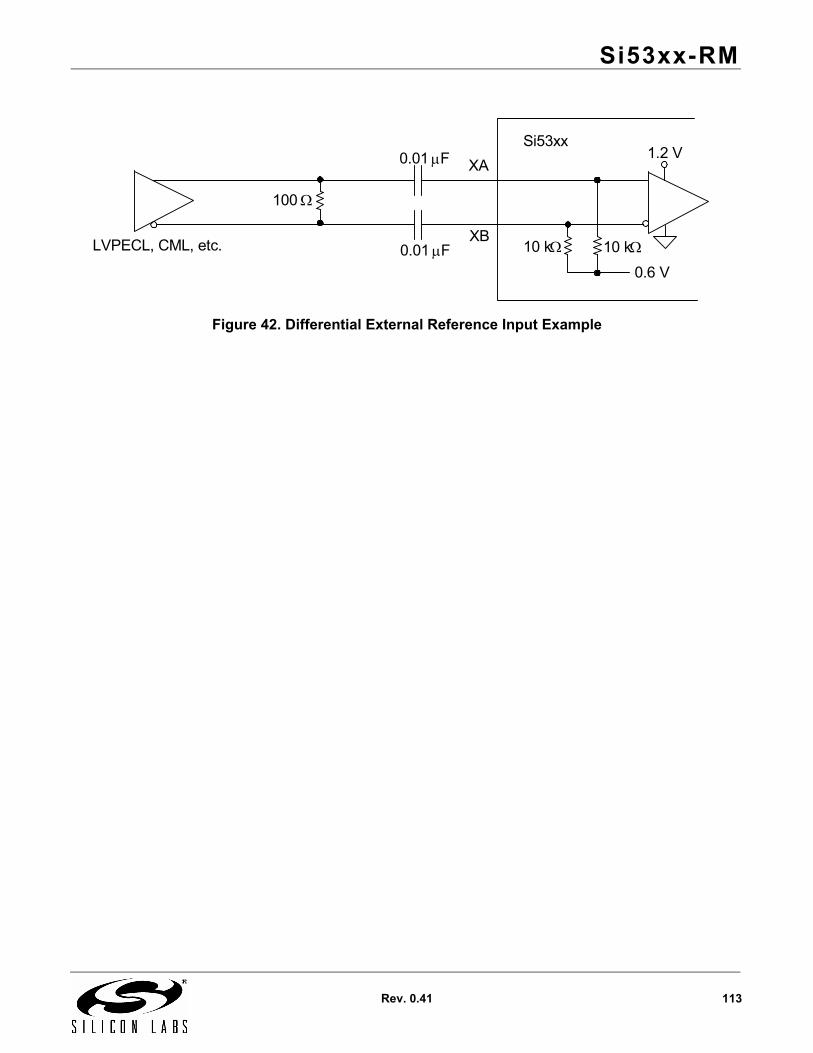
Si53xx-RM
Rev. 0.41 113
Figure 42. Differential External Reference Input Example
LVPECL, CML, etc.
0.01 F 1.2 V
0.6 V
Si53xx
XA
XB10 k
100
0.01 F 10 k
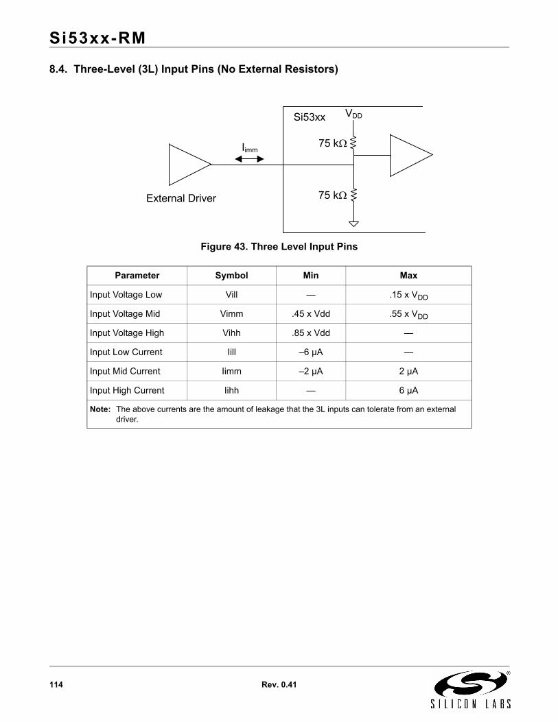
Si53xx-RM
114 Rev. 0.41
8.4. Three-Level (3L) Input Pins (No External Resistors)
Figure 43. Three Level Input Pins
Parameter Symbol Min Max
Input Voltage Low Vill — .15 x VDD
Input Voltage Mid Vimm .45 x Vdd .55 x VDD
Input Voltage High Vihh .85 x Vdd —
Input Low Current Iill –6 µA —
Input Mid Current Iimm –2 µA 2 µA
Input High Current Iihh — 6 µA
Note: The above currents are the amount of leakage that the 3L inputs can tolerate from an external driver.
External Driver
Si53xx
Iimm75 k
VDD
75 k
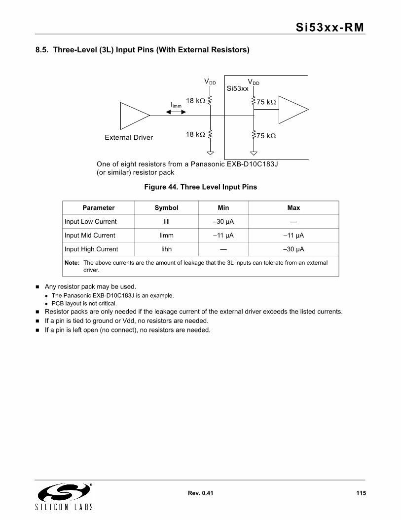
Si53xx-RM
Rev. 0.41 115
8.5. Three-Level (3L) Input Pins (With External Resistors)
Figure 44. Three Level Input Pins
Any resistor pack may be used.The Panasonic EXB-D10C183J is an example.PCB layout is not critical.
Resistor packs are only needed if the leakage current of the external driver exceeds the listed currents.
If a pin is tied to ground or Vdd, no resistors are needed.
If a pin is left open (no connect), no resistors are needed.
Parameter Symbol Min Max
Input Low Current Iill –30 µA —
Input Mid Current Iimm –11 µA –11 µA
Input High Current Iihh — –30 µA
Note: The above currents are the amount of leakage that the 3L inputs can tolerate from an external driver.
External Driver
Si53xx
Iimm18 k
VDD
18 k
75 k
VDD
75 k
One of eight resistors from a Panasonic EXB-D10C183J (or similar) resistor pack
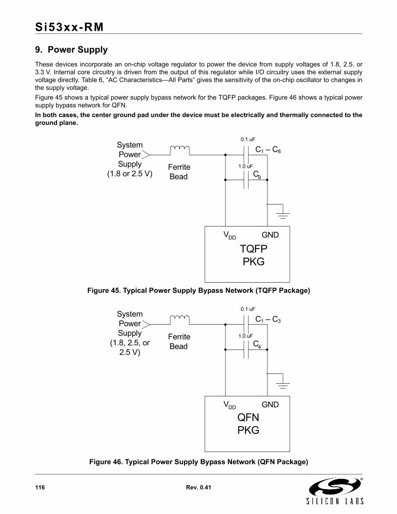
Si53xx-RM
116 Rev. 0.41
9. Power Supply
These devices incorporate an on-chip voltage regulator to power the device from supply voltages of 1.8, 2.5, or3.3 V. Internal core circuitry is driven from the output of this regulator while I/O circuitry uses the external supplyvoltage directly. Table 6, “AC Characteristics—All Parts” gives the sensitivity of the on-chip oscillator to changes inthe supply voltage.
Figure 45 shows a typical power supply bypass network for the TQFP packages. Figure 46 shows a typical powersupply bypass network for QFN.
In both cases, the center ground pad under the device must be electrically and thermally connected to theground plane.
Figure 45. Typical Power Supply Bypass Network (TQFP Package)
Figure 46. Typical Power Supply Bypass Network (QFN Package)
TQFPPKG
VDD GND
C1 – C8
C9
FerriteBead
System Power Supply
(1.8 or 2.5 V)
0.1 uF
1.0 uF
QFNPKG
VDD GND
C1 – C3
C4
FerriteBead
0.1 uF
1.0 uF
System Power Supply
(1.8, 2.5, or 2.5 V)
Si53xx-RM
Rev. 0.41 117
10. Packages and Ordering Guide
Please refer to the data sheet for your device.
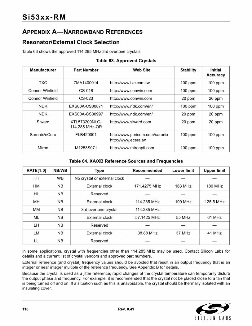
Si53xx-RM
118 Rev. 0.41
APPENDIX A—NARROWBAND REFERENCES
Resonator/External Clock Selection
Table 63 shows the approved 114.285 MHz 3rd overtone crystals.
In some applications, crystal with frequencies other than 114.285 MHz may be used. Contact Silicon Labs fordetails and a current list of crystal vendors and approved part numbers.
External reference (and crystal) frequency values should be avoided that result in an output frequency that is aninteger or near integer multiple of the reference frequency. See Appendix B for details.
Because the crystal is used as a jitter reference, rapid changes of the crystal temperature can temporarily disturbthe output phase and frequency. For example, it is recommended that the crystal not be placed close to a fan thatis being turned off and on. If a situation such as this is unavoidable, the crystal should be thermally isolated with aninsulating cover.
Table 63. Approved Crystals
Manufacturer Part Number Web Site Stability Initial Accuracy
TXC 7MA1400014 http://www.txc.com.tw 100 ppm 100 ppm
Connor Winfield CS-018 http://www.conwin.com 100 ppm 100 ppm
Connor Winfield CS-023 http://www.conwin.com 20 ppm 20 ppm
NDK EXS00A-CS00871 http://www.ndk.com/en/ 100 ppm 100 ppm
NDK EXS00A-CS00997 http://www.ndk.com/en/ 20 ppm 20 ppm
Siward XTL573200NLG-114.285 MHz-OR
http://www.siward.com 20 ppm 20 ppm
Saronix/eCera FLB420001 http://www.pericom.com/saronixhttp://www.ecera.tw
100 ppm 100 ppm
Mtron M1253S071 http://www.mtronpti.com 100 ppm 100 ppm
Table 64. XA/XB Reference Sources and Frequencies
RATE[1:0] NB/WB Type Recommended Lower limit Upper limit
HH WB No crystal or external clock — — —
HM NB External clock 171.4275 MHz 163 MHz 180 MHz
HL NB Reserved — — —
MH NB External clock 114.285 MHz 109 MHz 125.5 MHz
MM NB 3rd overtone crystal 114.285 MHz — —
ML NB External clock 57.1425 MHz 55 MHz 61 MHz
LH NB Reserved — — —
LM NB External clock 38.88 MHz 37 MHz 41 MHz
LL NB Reserved — — —
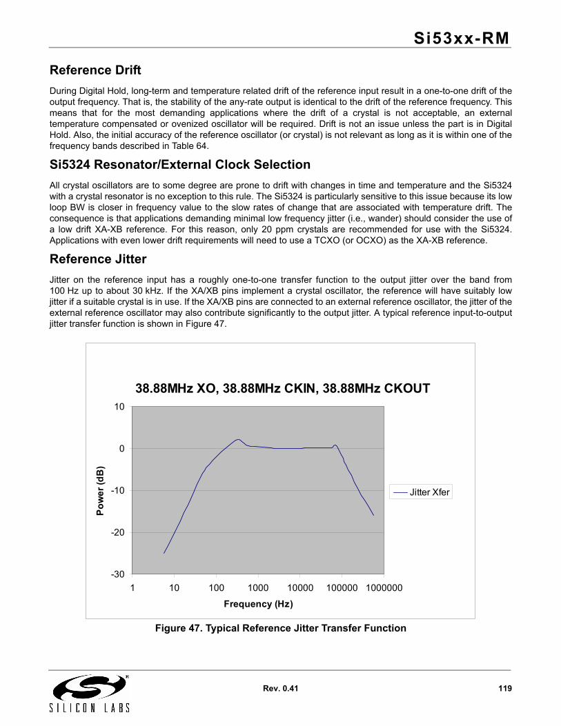
Si53xx-RM
Rev. 0.41 119
Reference Drift
During Digital Hold, long-term and temperature related drift of the reference input result in a one-to-one drift of theoutput frequency. That is, the stability of the any-rate output is identical to the drift of the reference frequency. Thismeans that for the most demanding applications where the drift of a crystal is not acceptable, an externaltemperature compensated or ovenized oscillator will be required. Drift is not an issue unless the part is in DigitalHold. Also, the initial accuracy of the reference oscillator (or crystal) is not relevant as long as it is within one of thefrequency bands described in Table 64.
Si5324 Resonator/External Clock Selection
All crystal oscillators are to some degree are prone to drift with changes in time and temperature and the Si5324with a crystal resonator is no exception to this rule. The Si5324 is particularly sensitive to this issue because its lowloop BW is closer in frequency value to the slow rates of change that are associated with temperature drift. Theconsequence is that applications demanding minimal low frequency jitter (i.e., wander) should consider the use ofa low drift XA-XB reference. For this reason, only 20 ppm crystals are recommended for use with the Si5324.Applications with even lower drift requirements will need to use a TCXO (or OCXO) as the XA-XB reference.
Reference Jitter
Jitter on the reference input has a roughly one-to-one transfer function to the output jitter over the band from100 Hz up to about 30 kHz. If the XA/XB pins implement a crystal oscillator, the reference will have suitably lowjitter if a suitable crystal is in use. If the XA/XB pins are connected to an external reference oscillator, the jitter of theexternal reference oscillator may also contribute significantly to the output jitter. A typical reference input-to-outputjitter transfer function is shown in Figure 47.
Figure 47. Typical Reference Jitter Transfer Function
38.88MHz XO, 38.88MHz CKIN, 38.88MHz CKOUT
-30
-20
-10
0
10
1 10 100 1000 10000 100000 1000000
Frequency (Hz)
Po
we
r (d
B)
Jitter Xfer
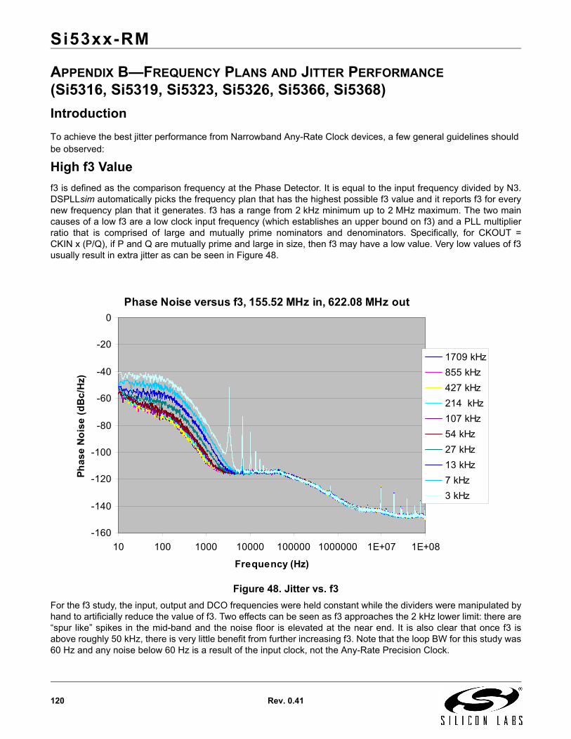
Si53xx-RM
120 Rev. 0.41
APPENDIX B—FREQUENCY PLANS AND JITTER PERFORMANCE (Si5316, Si5319, Si5323, Si5326, Si5366, Si5368)
Introduction
To achieve the best jitter performance from Narrowband Any-Rate Clock devices, a few general guidelines should be observed:
High f3 Value
f3 is defined as the comparison frequency at the Phase Detector. It is equal to the input frequency divided by N3.DSPLLsim automatically picks the frequency plan that has the highest possible f3 value and it reports f3 for everynew frequency plan that it generates. f3 has a range from 2 kHz minimum up to 2 MHz maximum. The two maincauses of a low f3 are a low clock input frequency (which establishes an upper bound on f3) and a PLL multiplierratio that is comprised of large and mutually prime nominators and denominators. Specifically, for CKOUT =CKIN x (P/Q), if P and Q are mutually prime and large in size, then f3 may have a low value. Very low values of f3usually result in extra jitter as can be seen in Figure 48.
Figure 48. Jitter vs. f3
For the f3 study, the input, output and DCO frequencies were held constant while the dividers were manipulated byhand to artificially reduce the value of f3. Two effects can be seen as f3 approaches the 2 kHz lower limit: there are“spur like” spikes in the mid-band and the noise floor is elevated at the near end. It is also clear that once f3 isabove roughly 50 kHz, there is very little benefit from further increasing f3. Note that the loop BW for this study was60 Hz and any noise below 60 Hz is a result of the input clock, not the Any-Rate Precision Clock.
Phase Noise versus f3, 155.52 MHz in, 622.08 MHz out
-160
-140
-120
-100
-80
-60
-40
-20
0
10 100 1000 10000 100000 1000000 1E+07 1E+08
Frequency (Hz)
Ph
as
e N
ois
e (
dB
c/H
z)
1709 kHz
855 kHz
427 kHz
214 kHz
107 kHz
54 kHz
27 kHz
13 kHz
7 kHz
3 kHz
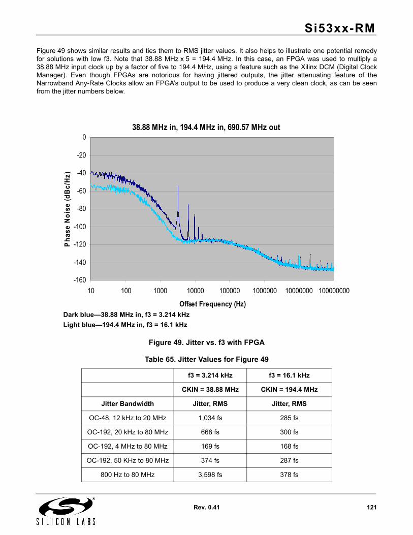
Si53xx-RM
Rev. 0.41 121
Figure 49 shows similar results and ties them to RMS jitter values. It also helps to illustrate one potential remedyfor solutions with low f3. Note that 38.88 MHz x 5 = 194.4 MHz. In this case, an FPGA was used to multiply a38.88 MHz input clock up by a factor of five to 194.4 MHz, using a feature such as the Xilinx DCM (Digital ClockManager). Even though FPGAs are notorious for having jittered outputs, the jitter attenuating feature of theNarrowband Any-Rate Clocks allow an FPGA’s output to be used to produce a very clean clock, as can be seenfrom the jitter numbers below.
Figure 49. Jitter vs. f3 with FPGA
Table 65. Jitter Values for Figure 49
f3 = 3.214 kHz f3 = 16.1 kHz
CKIN = 38.88 MHz CKIN = 194.4 MHz
Jitter Bandwidth Jitter, RMS Jitter, RMS
OC-48, 12 kHz to 20 MHz 1,034 fs 285 fs
OC-192, 20 kHz to 80 MHz 668 fs 300 fs
OC-192, 4 MHz to 80 MHz 169 fs 168 fs
OC-192, 50 KHz to 80 MHz 374 fs 287 fs
800 Hz to 80 MHz 3,598 fs 378 fs
38.88 MHz in, 194.4 MHz in, 690.57 MHz out
-160
-140
-120
-100
-80
-60
-40
-20
0
10 100 1000 10000 100000 1000000 10000000 100000000
Offset Frequency (Hz)
Ph
ase
No
ise
(dB
c/H
z)
Dark blue—38.88 MHz in, f3 = 3.214 kHz
Light blue—194.4 MHz in, f3 = 16.1 kHz
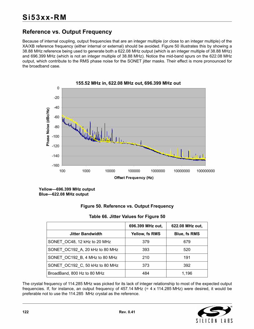
Si53xx-RM
122 Rev. 0.41
Reference vs. Output Frequency
Because of internal coupling, output frequencies that are an integer multiple (or close to an integer multiple) of theXA/XB reference frequency (either internal or external) should be avoided. Figure 50 illustrates this by showing a38.88 MHz reference being used to generate both a 622.08 MHz output (which is an integer multiple of 38.88 MHz)and 696.399 MHz (which is not an integer multiple of 38.88 MHz). Notice the mid-band spurs on the 622.08 MHzoutput, which contribute to the RMS phase noise for the SONET jitter masks. Their effect is more pronounced forthe broadband case.
Figure 50. Reference vs. Output Frequency
The crystal frequency of 114.285 MHz was picked for its lack of integer relationship to most of the expected outputfrequencies. If, for instance, an output frequency of 457.14 MHz (= 4 x 114.285 MHz) were desired, it would bepreferable not to use the 114.285 MHz crystal as the reference.
Table 66. Jitter Values for Figure 50
696.399 MHz out, 622.08 MHz out,
Jitter Bandwidth Yellow, fs RMS Blue, fs RMS
SONET_OC48, 12 kHz to 20 MHz 379 679
SONET_OC192_A, 20 kHz to 80 MHz 393 520
SONET_OC192_B, 4 MHz to 80 MHz 210 191
SONET_OC192_C, 50 kHz to 80 MHz 373 392
BroadBand, 800 Hz to 80 MHz 484 1,196
155.52 MHz in, 622.08 MHz out, 696.399 MHz out
-160
-140
-120
-100
-80
-60
-40
-20
0
100 1000 10000 100000 1000000 10000000 100000000
Offset Frequency (Hz)
Ph
ase
No
ise
(dB
c/H
z)
Yellow—696.399 MHz outputBlue—622.08 MHz output
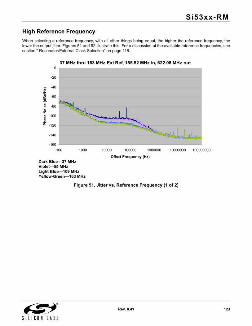
Si53xx-RM
Rev. 0.41 123
High Reference Frequency
When selecting a reference frequency, with all other things being equal, the higher the reference frequency, thelower the output jitter. Figures 51 and 52 illustrate this. For a discussion of the available reference frequencies, seesection " Resonator/External Clock Selection" on page 118.
Figure 51. Jitter vs. Reference Frequency (1 of 2)
37 MHz thru 163 MHz Ext Ref, 155.52 MHz in, 622.08 MHz out
-160
-140
-120
-100
-80
-60
-40
-20
0
100 1000 10000 100000 1000000 10000000 100000000
Offset Frequency (Hz)
Ph
ase
No
ise
(dB
c/H
z)
Dark Blue—37 MHzViolet—55 MHzLight Blue—109 MHzYellow-Green—163 MHz
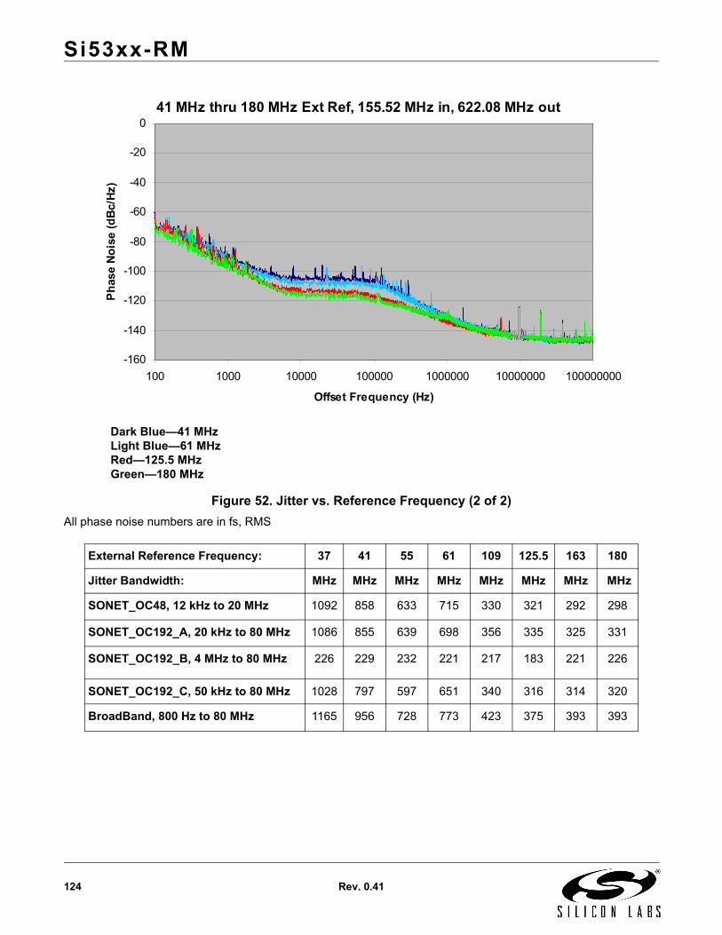
Si53xx-RM
124 Rev. 0.41
Figure 52. Jitter vs. Reference Frequency (2 of 2)
All phase noise numbers are in fs, RMS
External Reference Frequency: 37 41 55 61 109 125.5 163 180
Jitter Bandwidth: MHz MHz MHz MHz MHz MHz MHz MHz
SONET_OC48, 12 kHz to 20 MHz 1092 858 633 715 330 321 292 298
SONET_OC192_A, 20 kHz to 80 MHz 1086 855 639 698 356 335 325 331
SONET_OC192_B, 4 MHz to 80 MHz 226 229 232 221 217 183 221 226
SONET_OC192_C, 50 kHz to 80 MHz 1028 797 597 651 340 316 314 320
BroadBand, 800 Hz to 80 MHz 1165 956 728 773 423 375 393 393
41 MHz thru 180 MHz Ext Ref, 155.52 MHz in, 622.08 MHz out
-160
-140
-120
-100
-80
-60
-40
-20
0
100 1000 10000 100000 1000000 10000000 100000000
Offset Frequency (Hz)
Ph
ase
No
ise
(dB
c/H
z)
Dark Blue—41 MHzLight Blue—61 MHzRed—125.5 MHzGreen—180 MHz
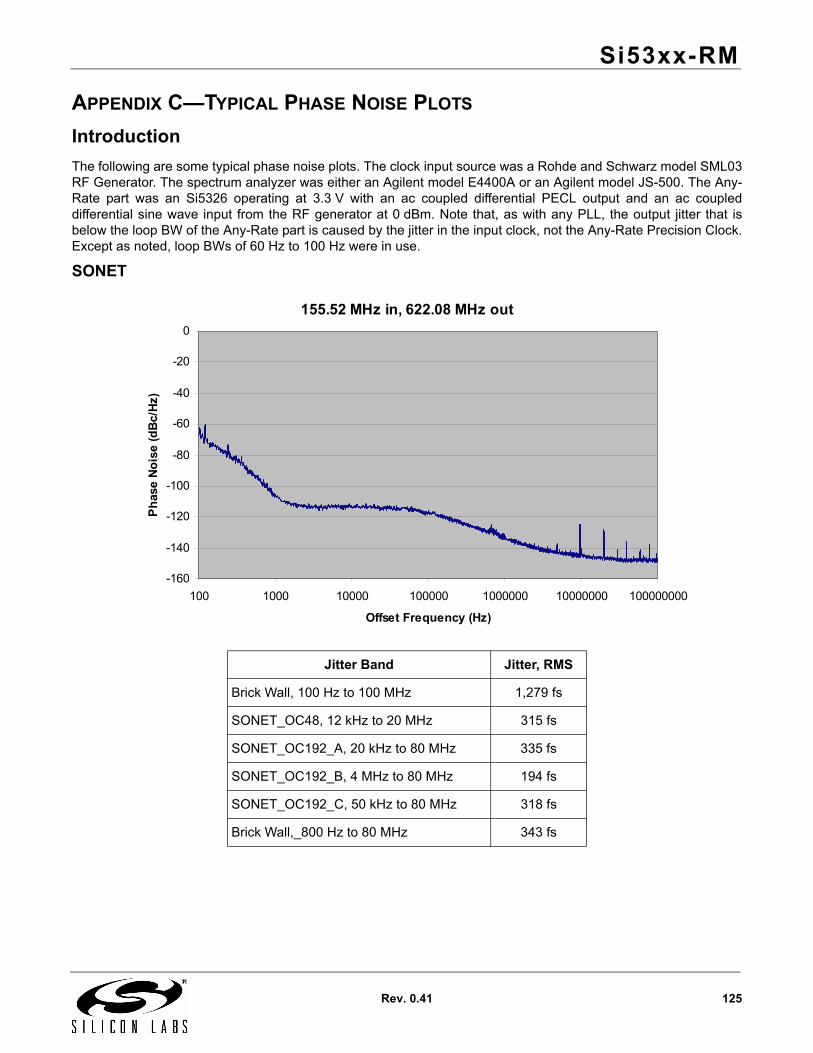
Si53xx-RM
Rev. 0.41 125
APPENDIX C—TYPICAL PHASE NOISE PLOTS
Introduction
The following are some typical phase noise plots. The clock input source was a Rohde and Schwarz model SML03RF Generator. The spectrum analyzer was either an Agilent model E4400A or an Agilent model JS-500. The Any-Rate part was an Si5326 operating at 3.3 V with an ac coupled differential PECL output and an ac coupleddifferential sine wave input from the RF generator at 0 dBm. Note that, as with any PLL, the output jitter that isbelow the loop BW of the Any-Rate part is caused by the jitter in the input clock, not the Any-Rate Precision Clock.Except as noted, loop BWs of 60 Hz to 100 Hz were in use.
SONET
Jitter Band Jitter, RMS
Brick Wall, 100 Hz to 100 MHz 1,279 fs
SONET_OC48, 12 kHz to 20 MHz 315 fs
SONET_OC192_A, 20 kHz to 80 MHz 335 fs
SONET_OC192_B, 4 MHz to 80 MHz 194 fs
SONET_OC192_C, 50 kHz to 80 MHz 318 fs
Brick Wall,_800 Hz to 80 MHz 343 fs
155.52 MHz in, 622.08 MHz out
-160
-140
-120
-100
-80
-60
-40
-20
0
100 1000 10000 100000 1000000 10000000 100000000
Offset Frequency (Hz)
Ph
ase
No
ise
(dB
c/H
z)
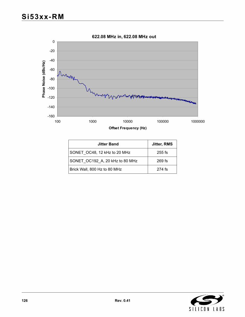
Si53xx-RM
126 Rev. 0.41
Jitter Band Jitter, RMS
SONET_OC48, 12 kHz to 20 MHz 255 fs
SONET_OC192_A, 20 kHz to 80 MHz 269 fs
Brick Wall, 800 Hz to 80 MHz 274 fs
622.08 MHz in, 622.08 MHz out
-160
-140
-120
-100
-80
-60
-40
-20
0
100 1000 10000 100000 1000000
Offset Frequency (Hz)
Ph
ase
No
ise
(dB
c/H
z)
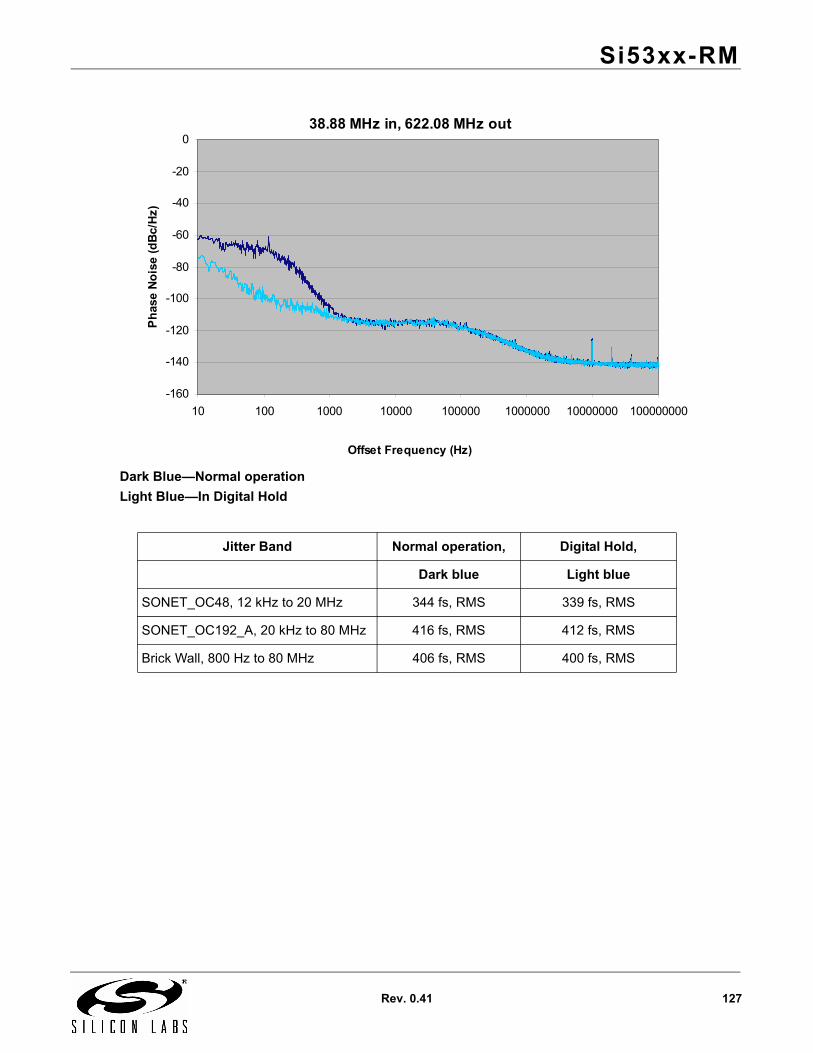
Si53xx-RM
Rev. 0.41 127
Jitter Band Normal operation, Digital Hold,
Dark blue Light blue
SONET_OC48, 12 kHz to 20 MHz 344 fs, RMS 339 fs, RMS
SONET_OC192_A, 20 kHz to 80 MHz 416 fs, RMS 412 fs, RMS
Brick Wall, 800 Hz to 80 MHz 406 fs, RMS 400 fs, RMS
38.88 MHz in, 622.08 MHz out
-160
-140
-120
-100
-80
-60
-40
-20
0
10 100 1000 10000 100000 1000000 10000000 100000000
Offset Frequency (Hz)
Ph
ase
No
ise
(dB
c/H
z)
Dark Blue—Normal operation
Light Blue—In Digital Hold
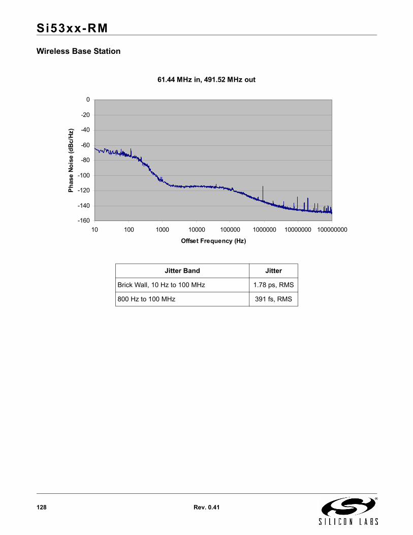
Si53xx-RM
128 Rev. 0.41
Wireless Base Station
Jitter Band Jitter
Brick Wall, 10 Hz to 100 MHz 1.78 ps, RMS
800 Hz to 100 MHz 391 fs, RMS
61.44 MHz in, 491.52 MHz out
-160
-140
-120
-100
-80
-60
-40
-20
0
10 100 1000 10000 100000 1000000 10000000 100000000
Offset Frequency (Hz)
Ph
ase
No
ise
(dB
c/H
z)
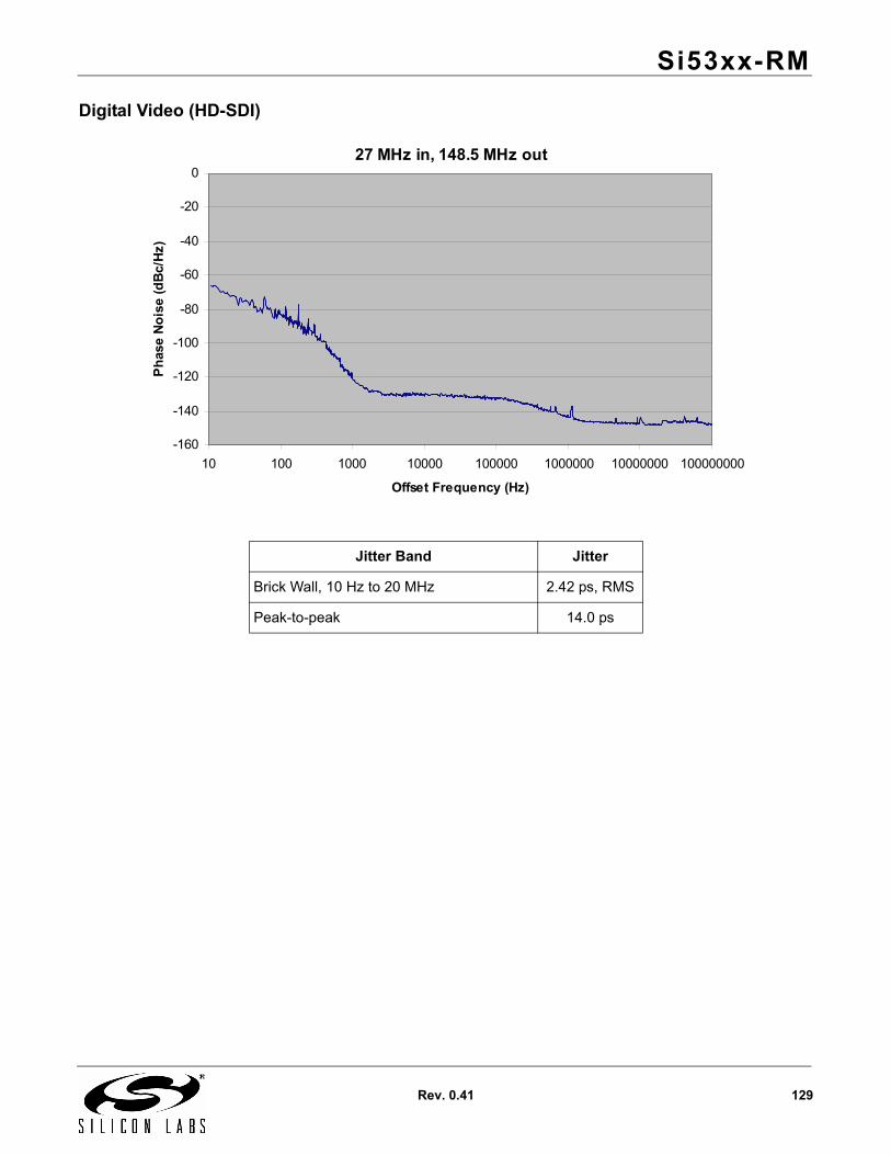
Si53xx-RM
Rev. 0.41 129
Digital Video (HD-SDI)
Jitter Band Jitter
Brick Wall, 10 Hz to 20 MHz 2.42 ps, RMS
Peak-to-peak 14.0 ps
27 MHz in, 148.5 MHz out
-160
-140
-120
-100
-80
-60
-40
-20
0
10 100 1000 10000 100000 1000000 10000000 100000000
Offset Frequency (Hz)
Ph
ase
No
ise
(dB
c/H
z)
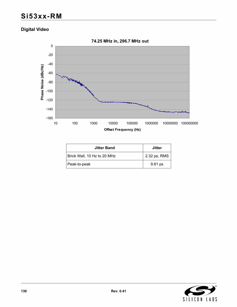
Si53xx-RM
130 Rev. 0.41
Digital Video
Jitter Band Jitter
Brick Wall, 10 Hz to 20 MHz 2.32 ps, RMS
Peak-to-peak 9.61 ps
74.25 MHz in, 296.7 MHz out
-160
-140
-120
-100
-80
-60
-40
-20
0
10 100 1000 10000 100000 1000000 10000000 100000000
Offset Frequency (Hz)
Ph
ase
No
ise
(dB
c/H
z)
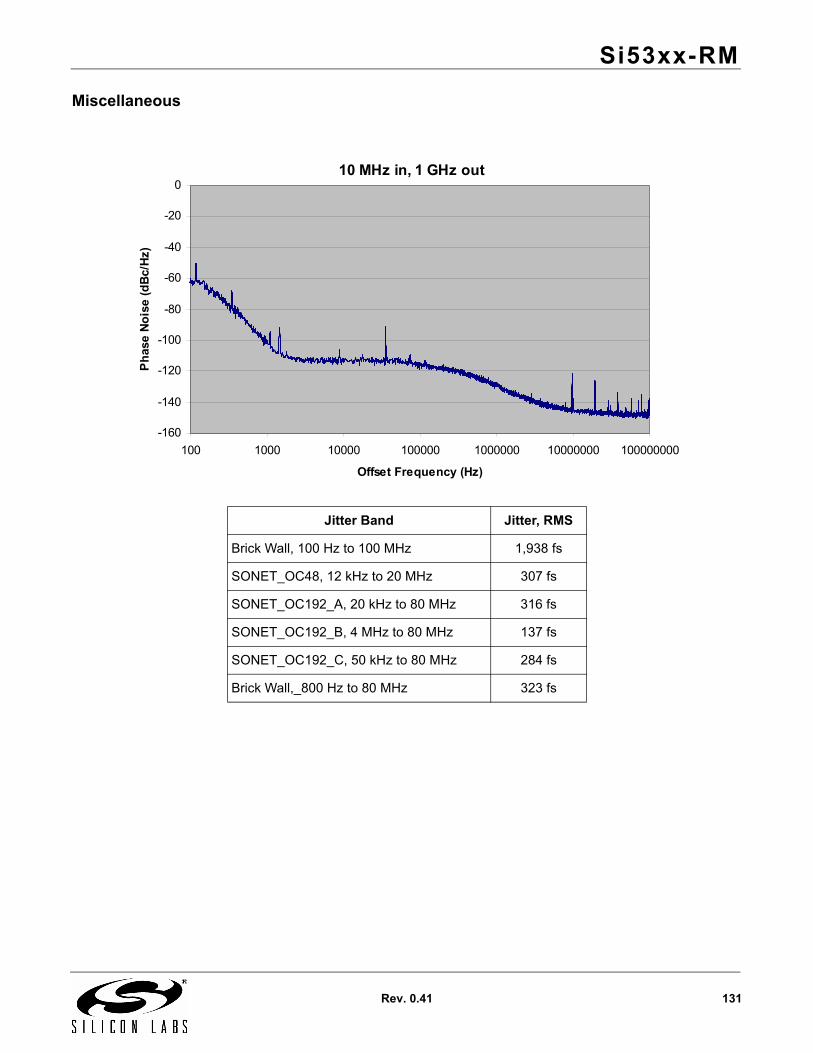
Si53xx-RM
Rev. 0.41 131
Miscellaneous
Jitter Band Jitter, RMS
Brick Wall, 100 Hz to 100 MHz 1,938 fs
SONET_OC48, 12 kHz to 20 MHz 307 fs
SONET_OC192_A, 20 kHz to 80 MHz 316 fs
SONET_OC192_B, 4 MHz to 80 MHz 137 fs
SONET_OC192_C, 50 kHz to 80 MHz 284 fs
Brick Wall,_800 Hz to 80 MHz 323 fs
10 MHz in, 1 GHz out
-160
-140
-120
-100
-80
-60
-40
-20
0
100 1000 10000 100000 1000000 10000000 100000000
Offset Frequency (Hz)
Ph
ase
No
ise
(dB
c/H
z)
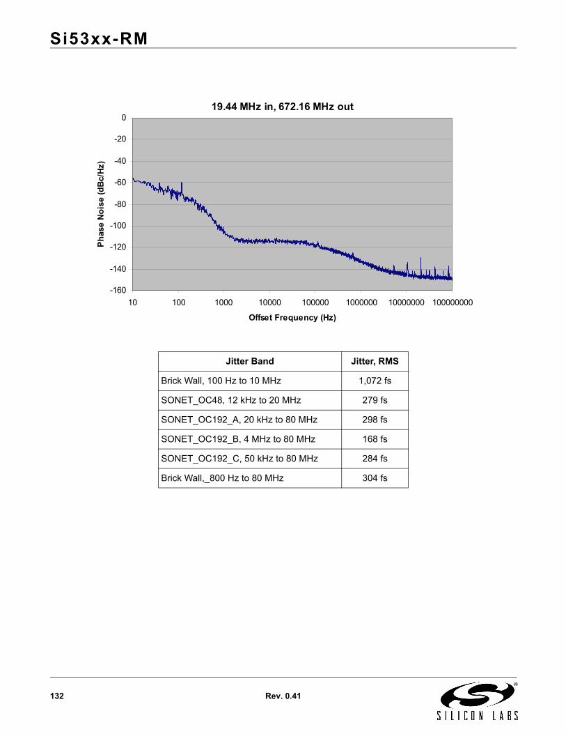
Si53xx-RM
132 Rev. 0.41
Jitter Band Jitter, RMS
Brick Wall, 100 Hz to 10 MHz 1,072 fs
SONET_OC48, 12 kHz to 20 MHz 279 fs
SONET_OC192_A, 20 kHz to 80 MHz 298 fs
SONET_OC192_B, 4 MHz to 80 MHz 168 fs
SONET_OC192_C, 50 kHz to 80 MHz 284 fs
Brick Wall,_800 Hz to 80 MHz 304 fs
19.44 MHz in, 672.16 MHz out
-160
-140
-120
-100
-80
-60
-40
-20
0
10 100 1000 10000 100000 1000000 10000000 100000000
Offset Frequency (Hz)
Ph
ase
No
ise
(dB
c/H
z)
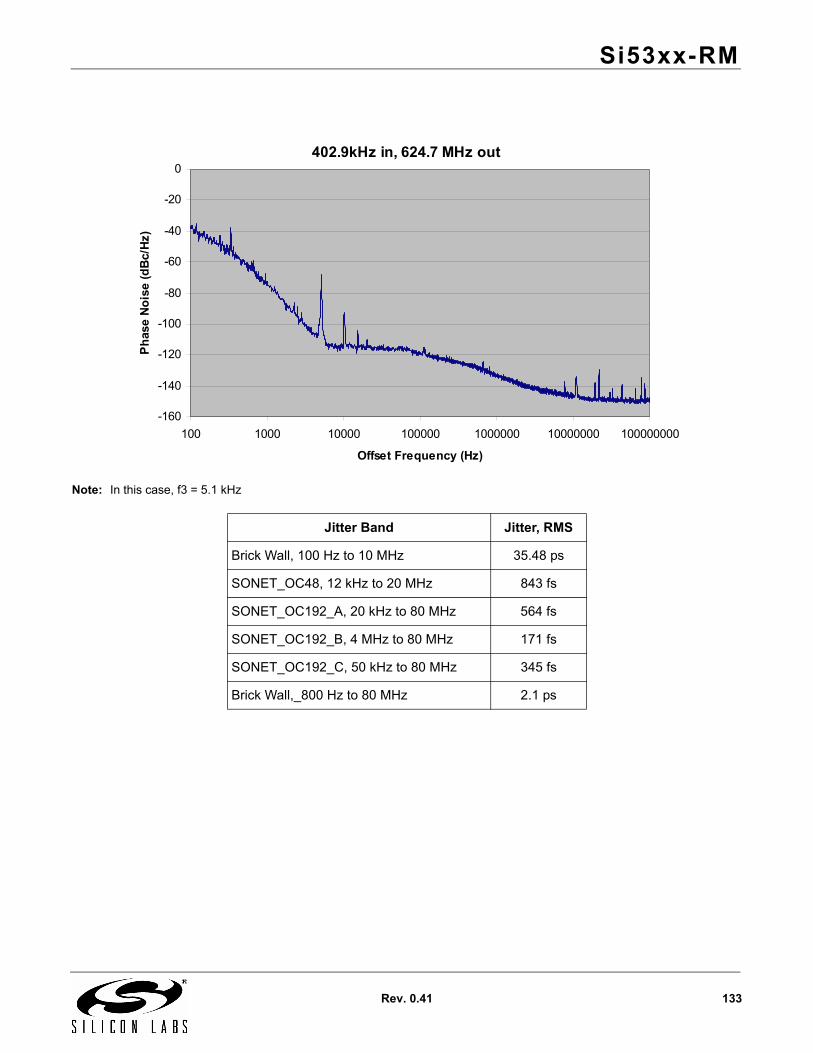
Si53xx-RM
Rev. 0.41 133
Note: In this case, f3 = 5.1 kHz
Jitter Band Jitter, RMS
Brick Wall, 100 Hz to 10 MHz 35.48 ps
SONET_OC48, 12 kHz to 20 MHz 843 fs
SONET_OC192_A, 20 kHz to 80 MHz 564 fs
SONET_OC192_B, 4 MHz to 80 MHz 171 fs
SONET_OC192_C, 50 kHz to 80 MHz 345 fs
Brick Wall,_800 Hz to 80 MHz 2.1 ps
402.9kHz in, 624.7 MHz out
-160
-140
-120
-100
-80
-60
-40
-20
0
100 1000 10000 100000 1000000 10000000 100000000
Offset Frequency (Hz)
Ph
ase
No
ise
(dB
c/H
z)
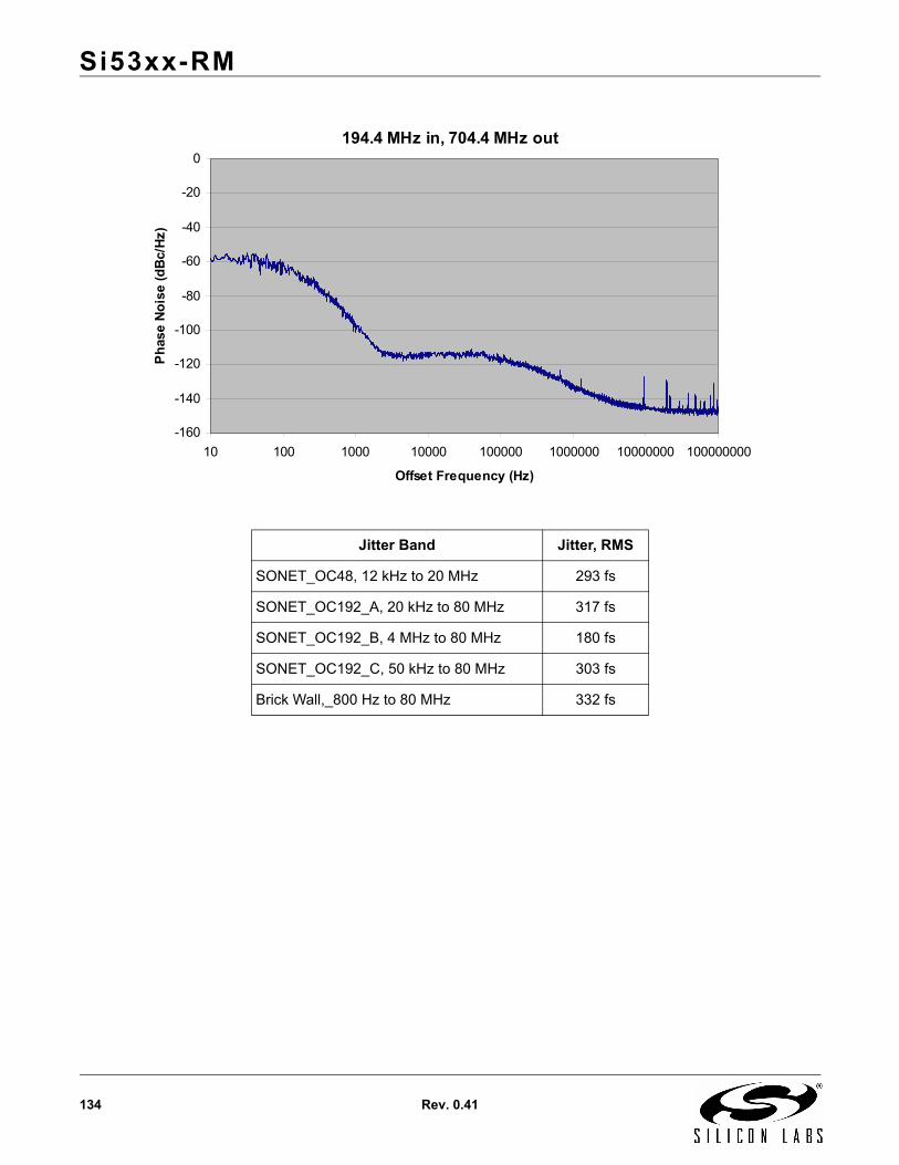
Si53xx-RM
134 Rev. 0.41
Jitter Band Jitter, RMS
SONET_OC48, 12 kHz to 20 MHz 293 fs
SONET_OC192_A, 20 kHz to 80 MHz 317 fs
SONET_OC192_B, 4 MHz to 80 MHz 180 fs
SONET_OC192_C, 50 kHz to 80 MHz 303 fs
Brick Wall,_800 Hz to 80 MHz 332 fs
194.4 MHz in, 704.4 MHz out
-160
-140
-120
-100
-80
-60
-40
-20
0
10 100 1000 10000 100000 1000000 10000000 100000000
Offset Frequency (Hz)
Ph
ase
No
ise
(dB
c/H
z)
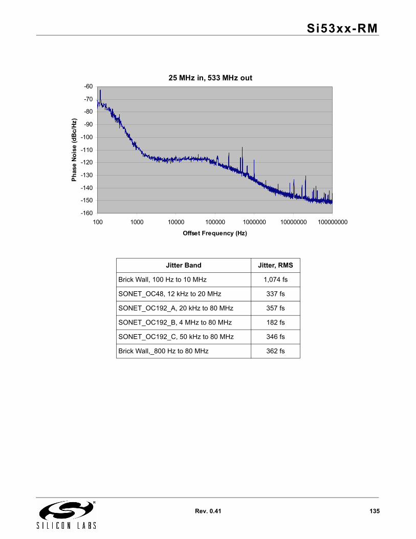
Si53xx-RM
Rev. 0.41 135
Jitter Band Jitter, RMS
Brick Wall, 100 Hz to 10 MHz 1,074 fs
SONET_OC48, 12 kHz to 20 MHz 337 fs
SONET_OC192_A, 20 kHz to 80 MHz 357 fs
SONET_OC192_B, 4 MHz to 80 MHz 182 fs
SONET_OC192_C, 50 kHz to 80 MHz 346 fs
Brick Wall,_800 Hz to 80 MHz 362 fs
25 MHz in, 533 MHz out
-160
-150
-140
-130
-120
-110
-100
-90
-80
-70
-60
100 1000 10000 100000 1000000 10000000 100000000
Offset Frequency (Hz)
Ph
ase
No
ise
(dB
c/H
z)

Si53xx-RM
136 Rev. 0.41
Jitter Band Jitter, RMS
Brick Wall, 100 Hz to 10 MHz 1,170 fs
SONET_OC48, 12 kHz to 20 MHz 281 fs
SONET_OC192_A, 20 kHz to 80 MHz 307 fs
SONET_OC192_B, 4 MHz to 80 MHz 176 fs
SONET_OC192_C, 50 kHz to 80 MHz 298 fs
Brick Wall,_800 Hz to 80 MHz 314 fs
25 MHz in, 666.7 MHz out
-160
-150
-140
-130
-120
-110
-100
-90
-80
-70
-60
100 1000 10000 100000 1000000 10000000 100000000
Offset Frequency (Hz)
Ph
ase
No
ise
(dB
c/H
z)
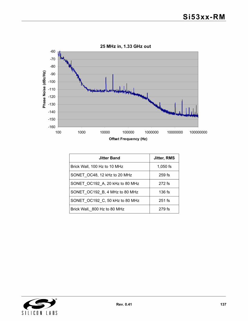
Si53xx-RM
Rev. 0.41 137
Jitter Band Jitter, RMS
Brick Wall, 100 Hz to 10 MHz 1,050 fs
SONET_OC48, 12 kHz to 20 MHz 259 fs
SONET_OC192_A, 20 kHz to 80 MHz 272 fs
SONET_OC192_B, 4 MHz to 80 MHz 136 fs
SONET_OC192_C, 50 kHz to 80 MHz 251 fs
Brick Wall,_800 Hz to 80 MHz 279 fs
25 MHz in, 1.33 GHz out
-160
-150
-140
-130
-120
-110
-100
-90
-80
-70
-60
100 1000 10000 100000 1000000 10000000 100000000
Offset Frequency (Hz)
Ph
ase
No
ise
(dB
c/H
z)
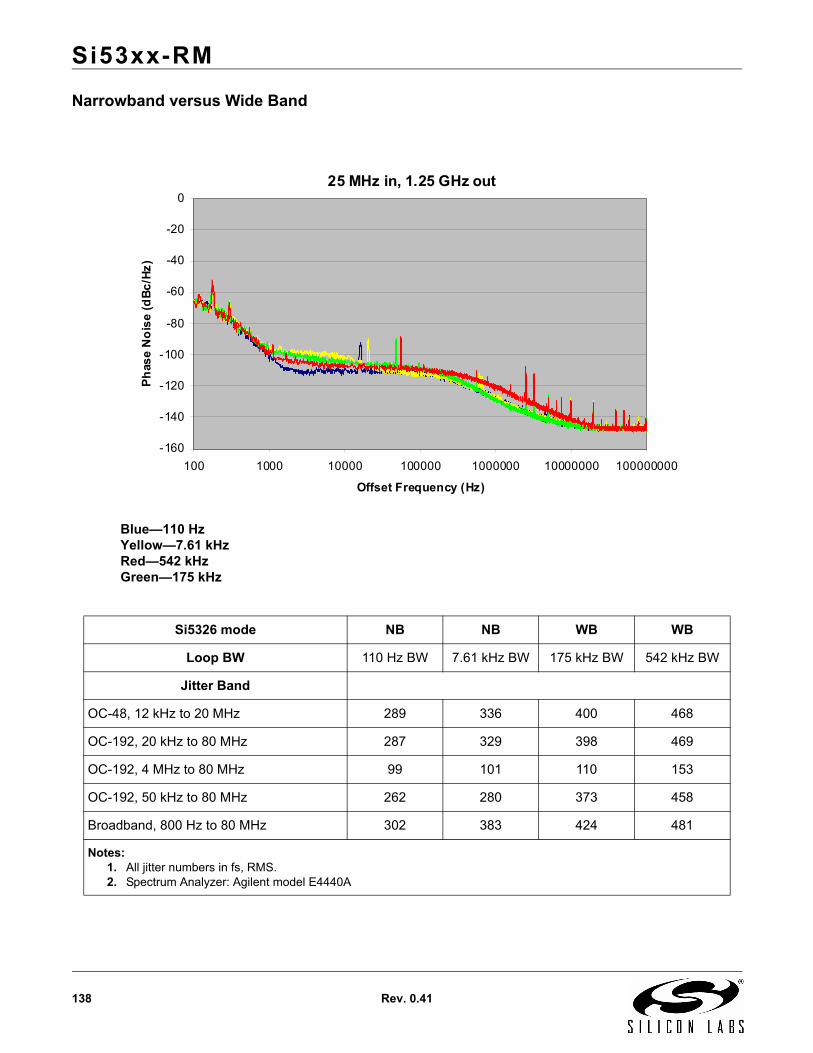
Si53xx-RM
138 Rev. 0.41
Narrowband versus Wide Band
Si5326 mode NB NB WB WB
Loop BW 110 Hz BW 7.61 kHz BW 175 kHz BW 542 kHz BW
Jitter Band
OC-48, 12 kHz to 20 MHz 289 336 400 468
OC-192, 20 kHz to 80 MHz 287 329 398 469
OC-192, 4 MHz to 80 MHz 99 101 110 153
OC-192, 50 kHz to 80 MHz 262 280 373 458
Broadband, 800 Hz to 80 MHz 302 383 424 481
Notes:1. All jitter numbers in fs, RMS.2. Spectrum Analyzer: Agilent model E4440A
Blue—110 HzYellow—7.61 kHzRed—542 kHzGreen—175 kHz
25 MHz in, 1.25 GHz out
-160
-140
-120
-100
-80
-60
-40
-20
0
100 1000 10000 100000 1000000 10000000 100000000
Offset Frequency (Hz)
Ph
ase
No
ise
(d
Bc
/Hz
)
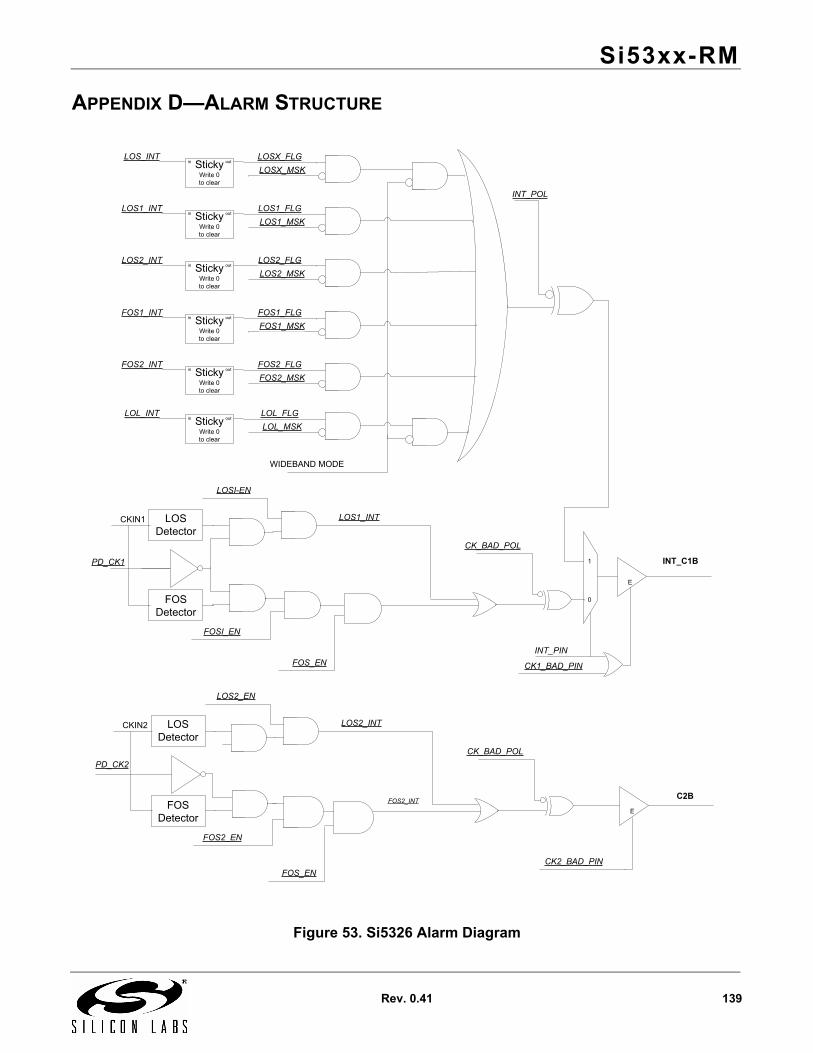
Si53xx-RM
Rev. 0.41 139
APPENDIX D—ALARM STRUCTURE
Figure 53. Si5326 Alarm Diagram
in outStickyWrite 0to clear
LOS_INT LOSX_FLGLOSX_MSK
in outStickyWrite 0to clear
LOL_INT LOL_FLGLOL_MSK
in outStickyWrite 0to clear
FOS2_INT FOS2_FLGFOS2_MSK
in outStickyWrite 0to clear
FOS1_INT FOS1_FLGFOS1_MSK
in outStickyWrite 0to clear
LOS2_INT LOS2_FLGLOS2_MSK
in outStickyWrite 0to clear
LOS1_INT LOS1_FLGLOS1_MSK
WIDEBAND MODE
INT_POL
FOSI_EN
LOSI-EN
INT_C1B
E
1
0
CK1_BAD_PIN
INT_PIN
CK_BAD_POL
LOS1_INTLOSDetector
FOSDetector
CKIN1
LOS2_EN
C2BE
CK2_BAD_PIN
CK_BAD_POL
LOS2_INTLOSDetector
FOSDetector
CKIN2
PD_CK1
PD_CK2
FOS2_INT
FOS2_EN
FOS_EN
FOS_EN
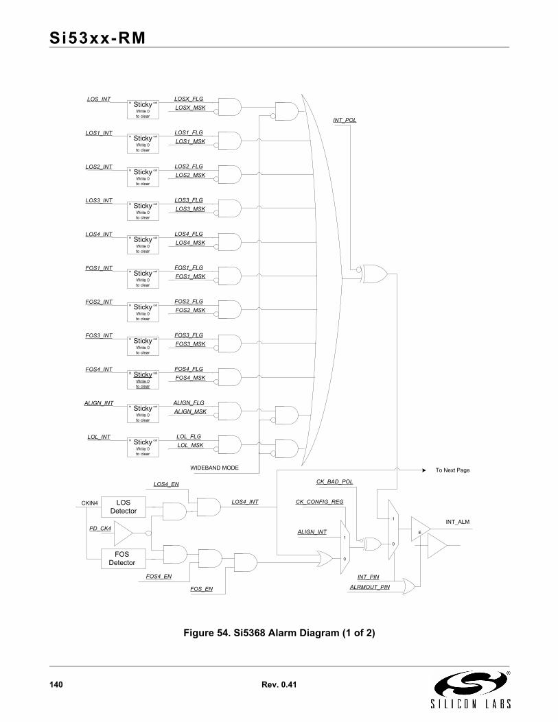
Si53xx-RM
140 Rev. 0.41
Figure 54. Si5368 Alarm Diagram (1 of 2)
in outStickyWrite 0to clear
LOS_INT LOSX_FLGLOSX_MSK
in outStickyWrite 0to clear
LOL_INT LOL_FLGLOL_MSK
in outStickyWrite 0to clear
FOS4_INT FOS4_FLGFOS4_MSK
in outStickyWrite 0to clear
FOS3_INT FOS3_FLGFOS3_MSK
in outStickyWrite 0to clear
FOS2_INT FOS2_FLGFOS2_MSK
in outStickyWrite 0to clear
FOS1_INT FOS1_FLGFOS1_MSK
in outStickyWrite 0to clear
LOS4_INT LOS4_FLGLOS4_MSK
in outStickyWrite 0to clear
LOS3_INT LOS3_FLGLOS3_MSK
in outStickyWrite 0to clear
LOS2_INT LOS2_FLGLOS2_MSK
in outStickyWrite 0to clear
LOS1_INT LOS1_FLGLOS1_MSK
in outStickyWrite 0to clear
ALIGN_INT ALIGN_FLGALIGN_MSK
WIDEBAND MODE
INT_POL
LOSDetector
FOSDetector
FOS4_EN
FOS_EN
LOS4_EN
INT_ALM
E
1
01
0
ALRMOUT_PIN
INT_PIN
CK_BAD_POL
LOS4_INT
ALIGN_INT
CK_CONFIG_REGCKIN4
PD_CK4
To Next Page
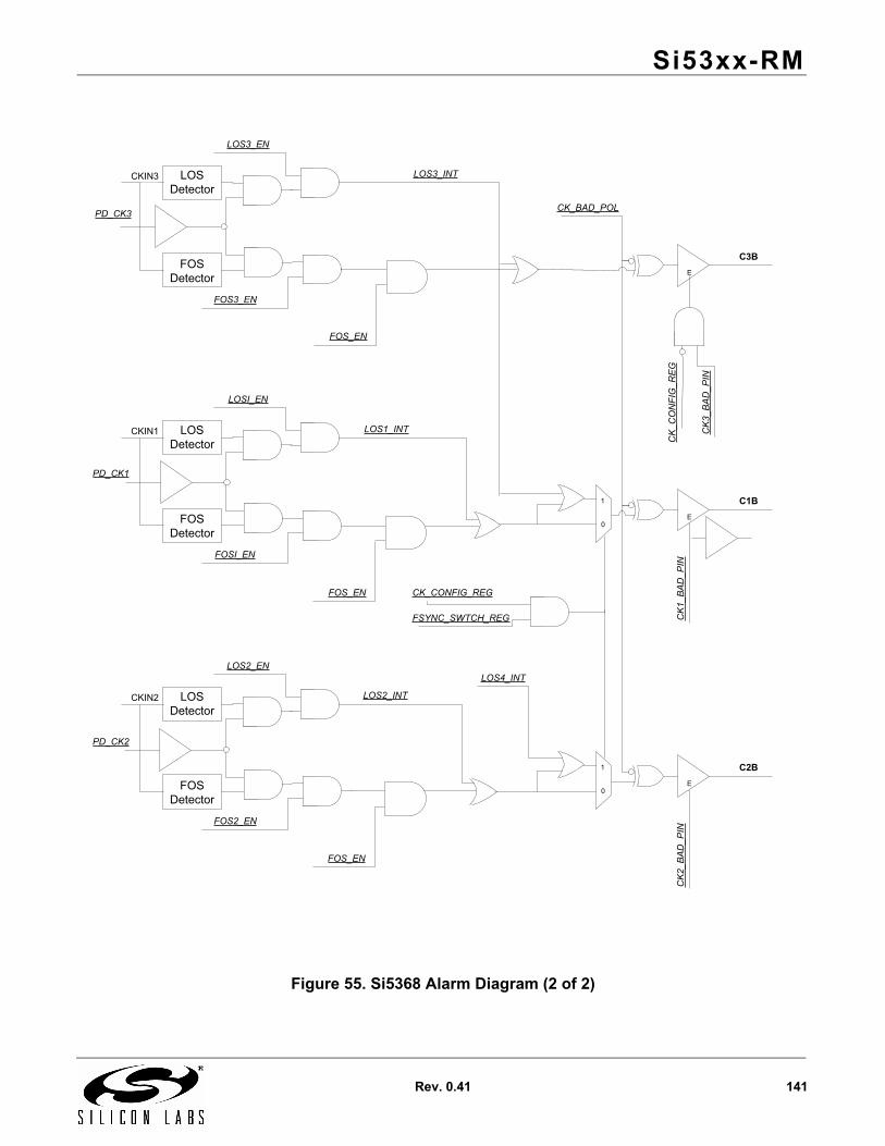
Si53xx-RM
Rev. 0.41 141
Figure 55. Si5368 Alarm Diagram (2 of 2)
LOSDetector
FOSDetector
FOS3_EN
LOS3_EN
LOS3_INT
C3BE
CK_BAD_POL
LOSDetector
FOSDetector
FOSI_EN
LOSI_EN
LOS1_INT
C1BE
1
0
LOSDetector
FOSDetector
FOS2_EN
LOS2_EN
LOS2_INT
C2BE
1
0
LOS4_INT
CK_CONFIG_REG
FSYNC_SWTCH_REG
CK3_BAD_PIN
CK_CONFIG_REG
CK1_BAD_PIN
CK2_BAD_PIN
CKIN2
CKIN1
CKIN3
PD_CK3
PD_CK1
PD_CK2
FOS_EN
FOS_EN
FOS_EN
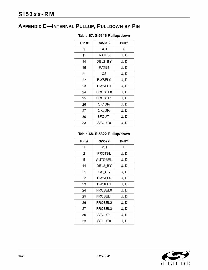
Si53xx-RM
142 Rev. 0.41
APPENDIX E—INTERNAL PULLUP, PULLDOWN BY PIN
Table 67. Si5316 Pullup/down
Pin # Si5316 Pull?
1 RST U
11 RATE0 U, D
14 DBL2_BY U, D
15 RATE1 U, D
21 CS U, D
22 BWSEL0 U, D
23 BWSEL1 U, D
24 FRQSEL0 U, D
25 FRQSEL1 U, D
26 CK1DIV U, D
27 CK2DIV U, D
30 SFOUT1 U, D
33 SFOUT0 U, D
Table 68. Si5322 Pullup/down
Pin # Si5322 Pull?
1 RST U
2 FRQTBL U, D
9 AUTOSEL U, D
14 DBL2_BY U, D
21 CS_CA U, D
22 BWSEL0 U, D
23 BWSEL1 U, D
24 FRQSEL0 U, D
25 FRQSEL1 U, D
26 FRQSEL2 U, D
27 FRQSEL3 U, D
30 SFOUT1 U, D
33 SFOUT0 U, D
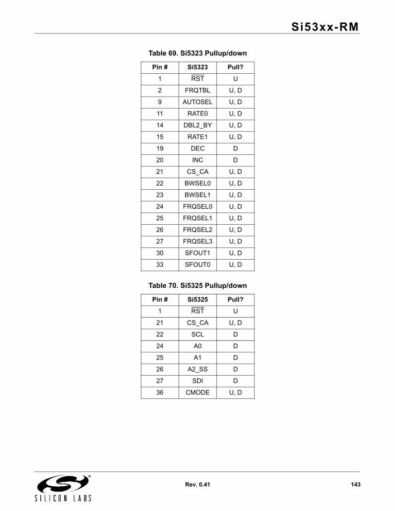
Si53xx-RM
Rev. 0.41 143
Table 69. Si5323 Pullup/down
Pin # Si5323 Pull?
1 RST U
2 FRQTBL U, D
9 AUTOSEL U, D
11 RATE0 U, D
14 DBL2_BY U, D
15 RATE1 U, D
19 DEC D
20 INC D
21 CS_CA U, D
22 BWSEL0 U, D
23 BWSEL1 U, D
24 FRQSEL0 U, D
25 FRQSEL1 U, D
26 FRQSEL2 U, D
27 FRQSEL3 U, D
30 SFOUT1 U, D
33 SFOUT0 U, D
Table 70. Si5325 Pullup/down
Pin # Si5325 Pull?
1 RST U
21 CS_CA U, D
22 SCL D
24 A0 D
25 A1 D
26 A2_SS D
27 SDI D
36 CMODE U, D
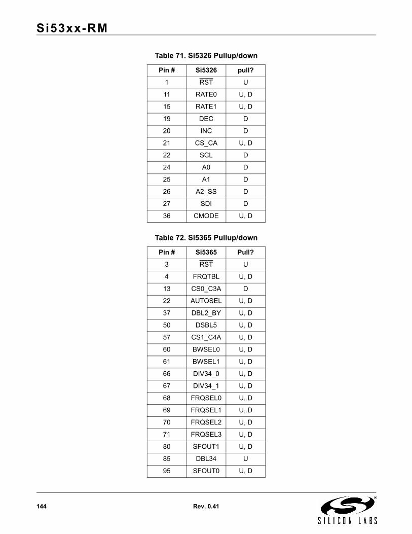
Si53xx-RM
144 Rev. 0.41
Table 71. Si5326 Pullup/down
Pin # Si5326 pull?
1 RST U
11 RATE0 U, D
15 RATE1 U, D
19 DEC D
20 INC D
21 CS_CA U, D
22 SCL D
24 A0 D
25 A1 D
26 A2_SS D
27 SDI D
36 CMODE U, D
Table 72. Si5365 Pullup/down
Pin # Si5365 Pull?
3 RST U
4 FRQTBL U, D
13 CS0_C3A D
22 AUTOSEL U, D
37 DBL2_BY U, D
50 DSBL5 U, D
57 CS1_C4A U, D
60 BWSEL0 U, D
61 BWSEL1 U, D
66 DIV34_0 U, D
67 DIV34_1 U, D
68 FRQSEL0 U, D
69 FRQSEL1 U, D
70 FRQSEL2 U, D
71 FRQSEL3 U, D
80 SFOUT1 U, D
85 DBL34 U
95 SFOUT0 U, D

Si53xx-RM
Rev. 0.41 145
Table 73. Si5366 Pullup/down
Pin # Si5366 Pull?
3 RST U
4 FRQTBL U, D
13 CS0_C3A D
20 FS_SW D
21 FS_ALIGN D
22 AUTOSEL U, D
32 RATE0 U, D
37 DBL2_BY U, D
42 RATE1 U, D
50 DBL_FS U, D
51 CK_CONF D
54 DEC D
55 INC D
56 FOS_CTL U, D
57 CS1_C4A U, D
60 BWSEL0 U, D
61 BWSEL1 U, D
66 DIV34_0 U, D
67 DIV34_1 U, D
68 FRQSEL0 U, D
69 FRQSEL1 U, D
70 FRQSEL2 U, D
71 FRQSEL3 U, D
80 SFOUT1 U, D
85 DSBL34 U
95 SFOUT0 U, D
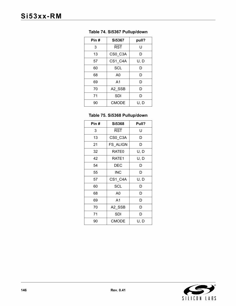
Si53xx-RM
146 Rev. 0.41
Table 74. Si5367 Pullup/down
Pin # Si5367 pull?
3 RST U
13 CS0_C3A D
57 CS1_C4A U, D
60 SCL D
68 A0 D
69 A1 D
70 A2_SSB D
71 SDI D
90 CMODE U, D
Table 75. Si5368 Pullup/down
Pin # Si5368 Pull?
3 RST U
13 CS0_C3A D
21 FS_ALIGN D
32 RATE0 U, D
42 RATE1 U, D
54 DEC D
55 INC D
57 CS1_C4A U, D
60 SCL D
68 A0 D
69 A1 D
70 A2_SSB D
71 SDI D
90 CMODE U, D
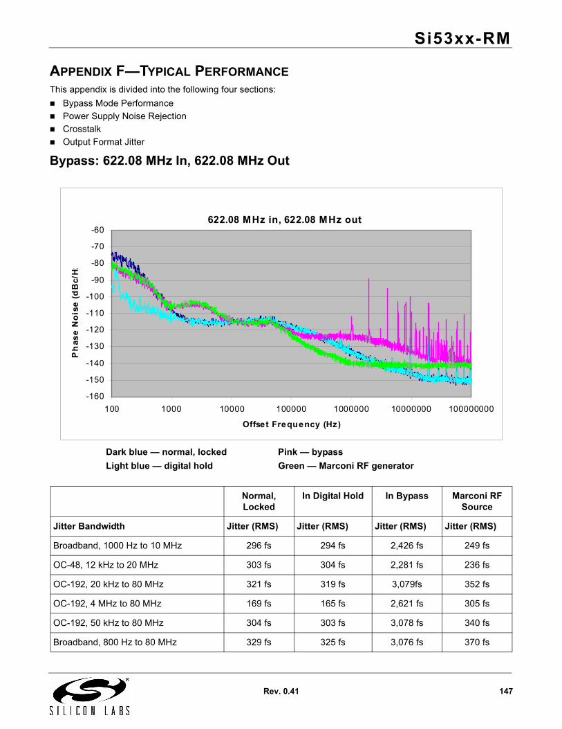
Si53xx-RM
Rev. 0.41 147
APPENDIX F—TYPICAL PERFORMANCE
This appendix is divided into the following four sections:
Bypass Mode Performance
Power Supply Noise Rejection
Crosstalk
Output Format Jitter
Bypass: 622.08 MHz In, 622.08 MHz Out
Normal, Locked
In Digital Hold In Bypass Marconi RF Source
Jitter Bandwidth Jitter (RMS) Jitter (RMS) Jitter (RMS) Jitter (RMS)
Broadband, 1000 Hz to 10 MHz 296 fs 294 fs 2,426 fs 249 fs
OC-48, 12 kHz to 20 MHz 303 fs 304 fs 2,281 fs 236 fs
OC-192, 20 kHz to 80 MHz 321 fs 319 fs 3,079fs 352 fs
OC-192, 4 MHz to 80 MHz 169 fs 165 fs 2,621 fs 305 fs
OC-192, 50 kHz to 80 MHz 304 fs 303 fs 3,078 fs 340 fs
Broadband, 800 Hz to 80 MHz 329 fs 325 fs 3,076 fs 370 fs
Dark blue — normal, locked Pink — bypass
Light blue — digital hold Green — Marconi RF generator
622.08 MHz in, 622.08 MHz out
-160
-150
-140
-130
-120
-110
-100
-90
-80
-70
-60
100 1000 10000 100000 1000000 10000000 100000000
Offset Frequency (Hz)
Ph
as
e N
ois
e (
dB
c/H
z
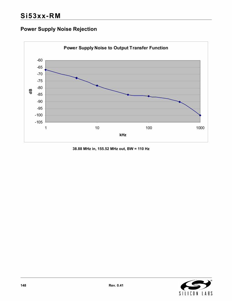
Si53xx-RM
148 Rev. 0.41
Power Supply Noise Rejection
Power Supply Noise to Output Transfer Function
-105
-100
-95
-90
-85
-80
-75
-70
-65
-60
1 10 100 1000
kHz
dB
38.88 MHz in, 155.52 MHz out, BW = 110 Hz
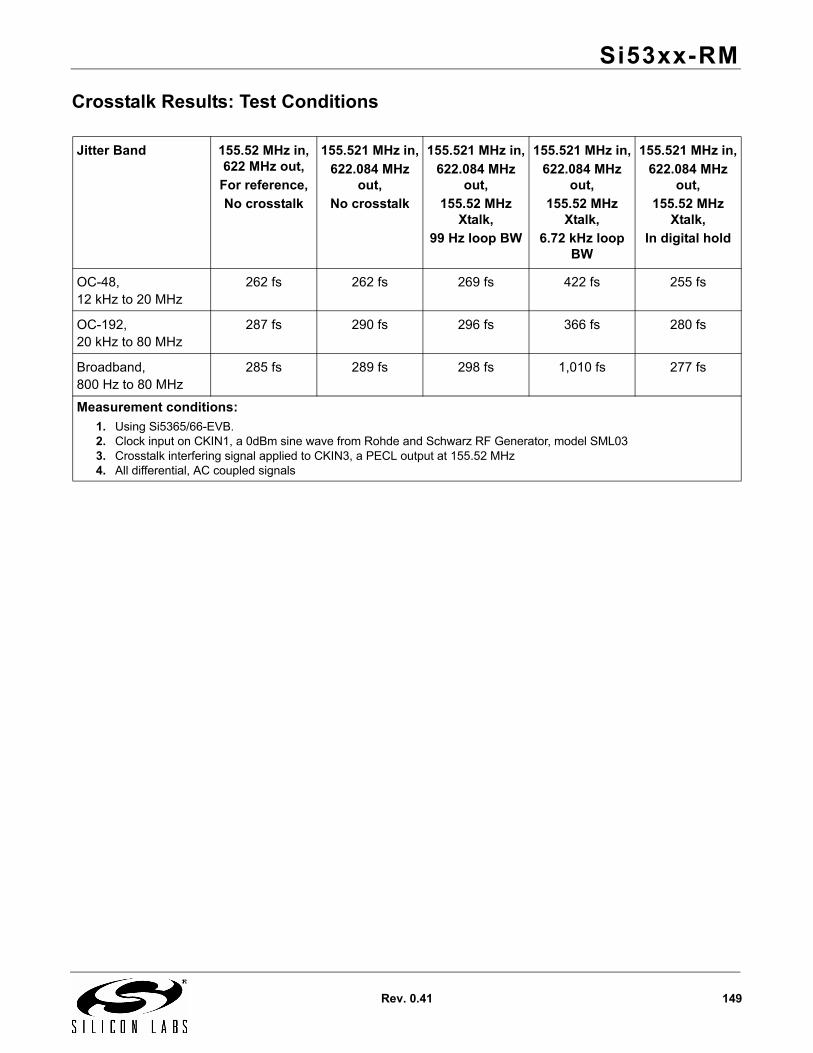
Si53xx-RM
Rev. 0.41 149
Crosstalk Results: Test Conditions
Jitter Band 155.52 MHz in, 622 MHz out,
For reference,
No crosstalk
155.521 MHz in,
622.084 MHz out,
No crosstalk
155.521 MHz in,
622.084 MHz out,
155.52 MHz Xtalk,
99 Hz loop BW
155.521 MHz in,
622.084 MHz out,
155.52 MHz Xtalk,
6.72 kHz loop BW
155.521 MHz in,
622.084 MHz out,
155.52 MHz Xtalk,
In digital hold
OC-48, 12 kHz to 20 MHz
262 fs 262 fs 269 fs 422 fs 255 fs
OC-192, 20 kHz to 80 MHz
287 fs 290 fs 296 fs 366 fs 280 fs
Broadband, 800 Hz to 80 MHz
285 fs 289 fs 298 fs 1,010 fs 277 fs
Measurement conditions:
1. Using Si5365/66-EVB.2. Clock input on CKIN1, a 0dBm sine wave from Rohde and Schwarz RF Generator, model SML033. Crosstalk interfering signal applied to CKIN3, a PECL output at 155.52 MHz 4. All differential, AC coupled signals
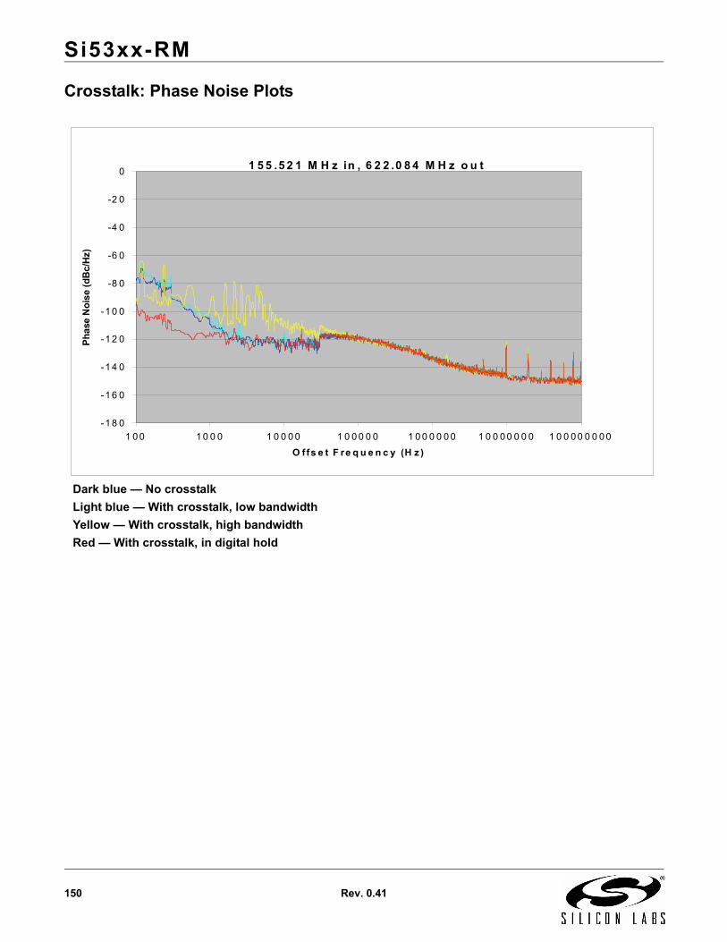
Si53xx-RM
150 Rev. 0.41
Crosstalk: Phase Noise Plots
Dark blue — No crosstalk
Light blue — With crosstalk, low bandwidth
Yellow — With crosstalk, high bandwidth
Red — With crosstalk, in digital hold
1 5 5 .5 2 1 M H z in , 6 2 2 .0 8 4 M H z o u t
-1 8 0
-1 6 0
-1 4 0
-1 2 0
-1 0 0
-8 0
-6 0
-4 0
-2 0
0
1 0 0 1 0 0 0 1 0 0 0 0 1 0 0 0 0 0 1 0 0 0 0 0 0 1 0 0 0 0 0 0 0 1 0 0 0 0 0 0 0 0
O ffs e t F re q u e n c y (H z )
Ph
ase
No
ise
(dB
c/H
z)
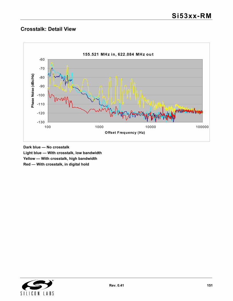
Si53xx-RM
Rev. 0.41 151
Crosstalk: Detail View
Dark blue — No crosstalk
Light blue — With crosstalk, low bandwidth
Yellow — With crosstalk, high bandwidth
Red — With crosstalk, in digital hold
155 .521 MHz in, 622 .084 MHz ou t
-130
-120
-110
-100
-90
-80
-70
-60
100 1000 10000 100000
Offset Frequency (Hz)
Pha
se N
oise
(dB
c/H
z)
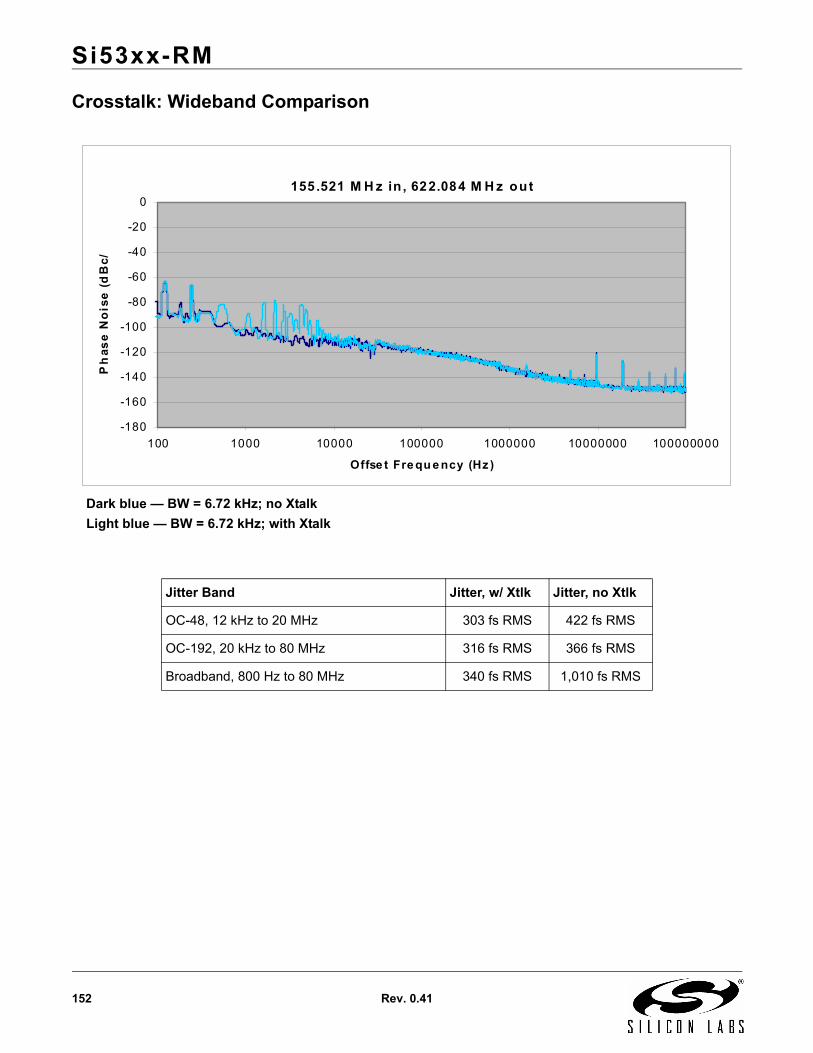
Si53xx-RM
152 Rev. 0.41
Crosstalk: Wideband Comparison
Jitter Band Jitter, w/ Xtlk Jitter, no Xtlk
OC-48, 12 kHz to 20 MHz 303 fs RMS 422 fs RMS
OC-192, 20 kHz to 80 MHz 316 fs RMS 366 fs RMS
Broadband, 800 Hz to 80 MHz 340 fs RMS 1,010 fs RMS
155 .521 M H z in , 622.084 M H z out
-180
-160
-140
-120
-100
-80
-60
-40
-20
0
100 1000 10000 100000 1000000 10000000 100000000
Offse t Fre qu e ncy (Hz )
Ph
as
e N
ois
e (
dB
c/
Dark blue — BW = 6.72 kHz; no Xtalk
Light blue — BW = 6.72 kHz; with Xtalk
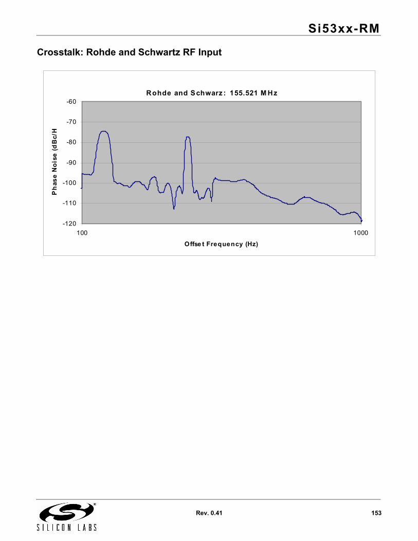
Si53xx-RM
Rev. 0.41 153
Crosstalk: Rohde and Schwartz RF Input
Rohde and Schwarz : 155.521 M Hz
-120
-110
-100
-90
-80
-70
-60
100 1000
Offse t Frequency (Hz)
Ph
as
e N
ois
e (
dB
c/H
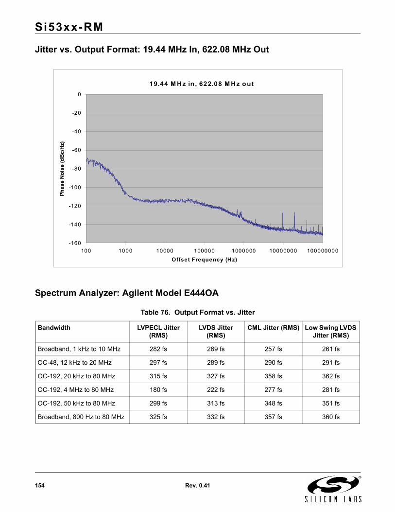
Si53xx-RM
154 Rev. 0.41
Jitter vs. Output Format: 19.44 MHz In, 622.08 MHz Out
Spectrum Analyzer: Agilent Model E444OA
Table 76. Output Format vs. Jitter
Bandwidth LVPECL Jitter (RMS)
LVDS Jitter (RMS)
CML Jitter (RMS) Low Swing LVDS Jitter (RMS)
Broadband, 1 kHz to 10 MHz 282 fs 269 fs 257 fs 261 fs
OC-48, 12 kHz to 20 MHz 297 fs 289 fs 290 fs 291 fs
OC-192, 20 kHz to 80 MHz 315 fs 327 fs 358 fs 362 fs
OC-192, 4 MHz to 80 MHz 180 fs 222 fs 277 fs 281 fs
OC-192, 50 kHz to 80 MHz 299 fs 313 fs 348 fs 351 fs
Broadband, 800 Hz to 80 MHz 325 fs 332 fs 357 fs 360 fs
19.44 M Hz in , 622.08 M Hz out
-160
-140
-120
-100
-80
-60
-40
-20
0
100 1000 10000 100000 1000000 10000000 100000000
Offset Frequency (H z)
Ph
ase
No
ise
(dB
c/H
z)
Si53xx-RM
Rev. 0.41 155
DOCUMENT CHANGE LIST
Revision 0.3 to Revision 0.4 Updated AC Specifications in Table 6, “AC
Characteristics—All Parts”
Added Si5365, Si5366, Si5367, and Si5368 operation at 3.3 V
Updated Section “7.8. Frame Synchronization Realignment (Si5368 and CK_CONFIG_REG = 1)”
Added input clock control diagrams in Section “7.4. Microprocessor Input Clock Control”
Added new crystals into Table 63, “Approved Crystals”
Updated "Appendix D—Alarm Structure" on page 139
Added "Appendix F—Typical Performance" on page 147
Revision 0.4 to Revision 0.41 Added Si5324.
Si53xx-RM
156 Rev. 0.41
CONTACT INFORMATIONSilicon Laboratories Inc.
400 West Cesar ChavezAustin, TX 78701Tel: 1+(512) 416-8500Fax: 1+(512) 416-9669Toll Free: 1+(877) 444-3032
Email: [email protected]: www.silabs.com
Silicon Laboratories, Silicon Labs, and DSPLL are trademarks of Silicon Laboratories Inc.Other products or brandnames mentioned herein are trademarks or registered trademarks of their respective holders.
The information in this document is believed to be accurate in all respects at the time of publication but is subject to change without notice. Silicon Laboratories assumes no responsibility for errors and omissions, and disclaims responsibility for any consequences resulting from the use of information included herein. Additionally, Silicon Laboratories assumes no responsibility for the functioning of undescribed features or parameters. Silicon Laboratories reserves the right to make changes without further notice. Silicon Laboratories makes no warranty, rep-resentation or guarantee regarding the suitability of its products for any particular purpose, nor does Silicon Laboratories assume any liability arising out of the application or use of any product or circuit, and specifically disclaims any and all liability, including without limitation conse-quential or incidental damages. Silicon Laboratories products are not designed, intended, or authorized for use in applications intended to support or sustain life, or for any other application in which the failure of the Silicon Laboratories product could create a situation where per-sonal injury or death may occur. Should Buyer purchase or use Silicon Laboratories products for any such unintended or unauthorized ap-plication, Buyer shall indemnify and hold Silicon Laboratories harmless against all claims and damages.