Ansys Inc. · PDF file2 2012 ANSYS, Inc. November 14, ... – Fully automated HFSS port...
54
February 23, 2009 Inventory #002593 © 2012 ANSYS, Inc. Designer 8.0/HFSS 15.0 1 November 14, 2012 Large Scale EM Simulation Ansys Inc.
Transcript of Ansys Inc. · PDF file2 2012 ANSYS, Inc. November 14, ... – Fully automated HFSS port...

February 23, 2009 Inventory #002593
© 2012 ANSYS, Inc. Designer 8.0/HFSS 15.0 1 November 14, 2012
Large Scale EM Simulation
Ansys Inc.

February 23, 2009 Inventory #002593
© 2012 ANSYS, Inc. Designer 8.0/HFSS 15.0 2 November 14, 2012
Simulating a Large Scale EM Model
• Design and simulate a full assembly that is comprised of – A 10 GHz Voltage Controlled Oscillator – An Array of Dielectric Resonator Antennas – A Balanced Amplifier
• Individual components will be designed and key design
steps will be illustrated. The design tools are as follows. – VCO: HFSS for ECAD with Cadence Integration – Dielectric Resonator Antennas: HFSS – Balanced Amplifier: Designer circuit and HFSS for ECD in
Designer • Final assembly will be analyzed using HFSS for ECAD
within Designer

February 23, 2009 Inventory #002593
© 2012 ANSYS, Inc. Designer 8.0/HFSS 15.0 3 November 14, 2012
Extraction of a 10 GHz Voltage Controlled Oscillator using HFSS for ECAD with Cadence. This new capability allows Cadence users to create and setup on chip structures to be solved by HFSS while remaining within the Cadence Design Environment.
• Extracting a voltage controlled oscillator using the new HFSS for ECAD with Cadence Integration
Part One: Voltage Controlled Oscillator

February 23, 2009 Inventory #002593
© 2012 ANSYS, Inc. Designer 8.0/HFSS 15.0 4 November 14, 2012
Design Description
• Voltage Controlled Oscillator – Design 10 GHz Voltage Controlled Oscillator – Utilize the HFSS within Cadence functionality – Account for all parasitic effects from bondwires, leadframe, etc.

February 23, 2009 Inventory #002593
© 2012 ANSYS, Inc. Designer 8.0/HFSS 15.0 5 November 14, 2012
Design Flow from Cadence to HFSS Traditional Cadence/HFSS integration
GDS from Cadence
HFSS
Tech file for stack up for each gds file is needed
S-parameters
Equivalent circuit
Layout in Cadence
Create tech file only once for each process
Boundaries/materials/ports are automatically created in HFSS
Models
Manual annotation of models to Cadence environment
Automatic back-annotation of models to Cadence environment
Boundaries/materials/ports are manually created in HFSS
Tune the parameters
S- parameters Equivalent circuits
Solve
Solution setup is manually defined by user inside HFSS
Automatic solution setup that can be updated by user
HFS
S/C
adence Link

February 23, 2009 Inventory #002593
© 2012 ANSYS, Inc. Designer 8.0/HFSS 15.0 6 November 14, 2012
HFSS Solver on Demand within Ansoft Designer
• Enables users to: – Drive HFSS directly from the intuitive stack-up based layout interface of Ansoft Designer. – Set up ready-to-solve chip simulations directly from the Cadence Environment . – Create full 3-D HFSS models while working within Cadence layout tool.
• HFSS Solver on Demand Advantages: – Fully automated HFSS port creation and setup – Layout, Stackup, and Padstack Editors – Parametric Design Environment – Maintain Trace Characteristics and Nets from Layout – Hierarchical Design – Chip/Package/Board

February 23, 2009 Inventory #002593
© 2012 ANSYS, Inc. Designer 8.0/HFSS 15.0 7 November 14, 2012
HFSS for ECAD within Cadence
Cadence Environment
HFSS Model
HFSS/Cadence Integration
Model Back annotation

February 23, 2009 Inventory #002593
© 2012 ANSYS, Inc. Designer 8.0/HFSS 15.0 8 November 14, 2012
HFSS within Cadence: VCO
• Schematic and Layout:

February 23, 2009 Inventory #002593
© 2012 ANSYS, Inc. Designer 8.0/HFSS 15.0 9 November 14, 2012
1) Ports are automatically created 2) Option to Merge vias 3) Option to filter layout
Inductor capacitor
HFSS within Cadence: VCO Design Flow
HFSS/Cadence Link Non merged vias
Merged vias

February 23, 2009 Inventory #002593
© 2012 ANSYS, Inc. Designer 8.0/HFSS 15.0 10 November 14, 2012
VCO Design Back Annotation
HFSS symbol in schematic design

February 23, 2009 Inventory #002593
© 2012 ANSYS, Inc. Designer 8.0/HFSS 15.0 11 November 14, 2012
VCO Full Circuit Model
• Dynamically linked VCO Circuit and HFSS FEM Model

February 23, 2009 Inventory #002593
© 2012 ANSYS, Inc. Designer 8.0/HFSS 15.0 12 November 14, 2012
VCO Operating Frequency
200 MHz
550 MHz!
Red > Circuit Behavioral model Black > HFSS Inductor Model Blue > HFSS VCO Model

February 23, 2009 Inventory #002593
© 2012 ANSYS, Inc. Designer 8.0/HFSS 15.0 13 November 14, 2012
VCO Time Response
Red > Circuit Behavioral model Blue > HFSS Inductor Model Black > HFSS VCO Model

February 23, 2009 Inventory #002593
© 2012 ANSYS, Inc. Designer 8.0/HFSS 15.0 14 November 14, 2012
VCO Operating Frequency Tuning
• Varactors used to tune VCO Frequency to 10 GHz
VCO Frequency Response

February 23, 2009 Inventory #002593
© 2012 ANSYS, Inc. Designer 8.0/HFSS 15.0 15 November 14, 2012
Tuned VCO Final Results
• Results
VCO Frequency
VCO Transient Response
VCO Harmonics

February 23, 2009 Inventory #002593
© 2012 ANSYS, Inc. Designer 8.0/HFSS 15.0 16 November 14, 2012
Design of a 10 GHz dielectric resonator antenna using HFSS. Final antenna design will be incorporated into Designer and analyzed with HFSS for ECAD within Designer.
• Designing a Dielectric Resonator Antenna with HFSS
Part Two: Dielectric Resonator Antenna (DRA) Design

February 23, 2009 Inventory #002593
© 2012 ANSYS, Inc. Designer 8.0/HFSS 15.0 17 November 14, 2012
Motivations Behind The Use of DRA’s
• Dielectric resonator antennas (DRAs) are • alternatives to conventional antenna types • preferable for wireless communications systems due to
• their small size • high radiation efficiency (>98%) • wide impedance bandwidth • low ohmic loss…
• Can be made in various shapes for Antenna Applications :

February 23, 2009 Inventory #002593
© 2012 ANSYS, Inc. Designer 8.0/HFSS 15.0 18 November 14, 2012
Dielectric Resonators Uses
Dielectric Resonator Modes
High Q Modes Low Q Modes
Filtering & Oscillation Radiating Purposes
Dual Band Dielectric Resonator Antenna &
Filter
Dual Band Dielectric Resonator Antenna Dielectric Resonator Antenna
& Oscillator
Photos courtesy of Laila Salman PhD

February 23, 2009 Inventory #002593
© 2012 ANSYS, Inc. Designer 8.0/HFSS 15.0 19 November 14, 2012
Excitation Techniques
Aperture Coupling Probe Coupling Microstrip Line
Dielectric Image Guide Coupling
Coplanar Coupling
Dielectric Resonator Coupling Mechanisms
Photos courtesy of Laila Salman PhD

February 23, 2009 Inventory #002593
© 2012 ANSYS, Inc. Designer 8.0/HFSS 15.0 20 November 14, 2012
Design Procedure / Challenges
• Proper Design of a DRA follows the following steps
– Select the Mode of Interest & the Operating Frequency Range • Linearly polarized • 10 GHz
– Obtain Dielectric Resonator Design Parameters
• Rectangular dielectric resonator
– Choose the Appropriate Excitation Technique
• Stripline with transition to microstrip feed • Small patch excitation

February 23, 2009 Inventory #002593
© 2012 ANSYS, Inc. Designer 8.0/HFSS 15.0 21 November 14, 2012
Field Distributions in DRA
Electric Field Distribution inside the DR (Side View)
Magnetic Field Distribution inside the DR (Top View)

February 23, 2009 Inventory #002593
© 2012 ANSYS, Inc. Designer 8.0/HFSS 15.0 22 November 14, 2012
High Dielectric Substrate
Low Dielectric Substrate
Microstrip Coupling
Via Transition
Stripline Feed
Side View (Stackup)
Dielectric Resonator
Design Challenges – Coupling Technique
Microstrip-to-Stripline Transition

February 23, 2009 Inventory #002593
© 2012 ANSYS, Inc. Designer 8.0/HFSS 15.0 23 November 14, 2012
Antenna Directivity Patters (Plane Cuts) @ 10GHz
DRA Results

February 23, 2009 Inventory #002593
© 2012 ANSYS, Inc. Designer 8.0/HFSS 15.0 24 November 14, 2012
Final Single Element DRA Design
DR, єr = 10.2
Meander Strip Line Feeding Network
Opening in GND Plane
Wave Port Excitation with PEC Cap
Patch / Microstrip Coupling

February 23, 2009 Inventory #002593
© 2012 ANSYS, Inc. Designer 8.0/HFSS 15.0 25 November 14, 2012
Final Single Element DRA Results

February 23, 2009 Inventory #002593
© 2012 ANSYS, Inc. Designer 8.0/HFSS 15.0 26 November 14, 2012
Final Single Element DRA Results
10 GHz Antenna Gain Radiation Pattern
10 GHz Antenna Directivity 3D Polar Plot

February 23, 2009 Inventory #002593
© 2012 ANSYS, Inc. Designer 8.0/HFSS 15.0 27 November 14, 2012
Dielectric Resonators
a b
c
єr = 10.2
Four Element DR Antenna Array

February 23, 2009 Inventory #002593
© 2012 ANSYS, Inc. Designer 8.0/HFSS 15.0 28 November 14, 2012
Full Array Far Field Results

February 23, 2009 Inventory #002593
© 2012 ANSYS, Inc. Designer 8.0/HFSS 15.0 29 November 14, 2012
A 10 GHZ balanced amplifier will be designed within ANSYS Designer. This design will utilize the UMS design kit as well as the HFSS for ECAD functionality. This will enable engineers to combine both circuit and electromagnetic solver in a hybrid circuit/field solver simulation, providing maximum accuracy.
• Designing a balanced amplifier with Designer
Part Three: Balanced Amplifier Design

February 23, 2009 Inventory #002593
© 2012 ANSYS, Inc. Designer 8.0/HFSS 15.0 30 November 14, 2012
Ansoft Designer Overview
• Design Technology – Circuit & System Analysis
• Time and Frequency Domain – Electromagnetic Analysis – Access Multiple Solvers
• HFSS, PlanarEM, Nexxim and HSPICE
• Design Management – Hierarchical Schematic and Layout (2D/3D) – Design Exploration
• Parameterization, Optimization, Sensitivity & Statistical – Bi-directional Links to Field Solvers
• HFSS, PlanarEM, SIwave, Q3D, 2D Extractor – 3rd Party Links for Models and Geometry
• High Performance Computing (Multi-core/GPU)
00
0
0
0
0
0
0
1
2
3
U1Trans_1x2
1
2
3
U2Trans_1x2

February 23, 2009 Inventory #002593
© 2012 ANSYS, Inc. Designer 8.0/HFSS 15.0 31 November 14, 2012
Powerful New Importing Capability
• Links for Cadence Allegro/APD/Virtuoso – Run from either Cadence or Designer – Design cutouts and wirebonds for critical nets – Tightly couples ECAD, Circuits and HFSS
• Links for ODB++
– Common PCB Manufacturing format – Translation path for Mentor, Zuken, – Cadence, Altium, …

February 23, 2009 Inventory #002593
© 2012 ANSYS, Inc. Designer 8.0/HFSS 15.0 32 November 14, 2012
Design Description
•Balanced Amplifier • Combine two MMIC Amplifiers in parallel • Incorporate amplifiers in separate packages • Combine Amplifiers and 90° Hybrids on board • Include on-board biasing for amplifiers

February 23, 2009 Inventory #002593
© 2012 ANSYS, Inc. Designer 8.0/HFSS 15.0 33 November 14, 2012
Amplifier Schematic
• Three Gain stages separated by Wilkinson dividers
AMPNL
AMPNL
AMPNL
AMPNL
AMPNL
AMPNL
AMPNL
AMPNL

February 23, 2009 Inventory #002593
© 2012 ANSYS, Inc. Designer 8.0/HFSS 15.0 34 November 14, 2012
90º Hybrid Design Overview
• Hybrid Applications • Power Splitter / Combiner
• Load on one of the input / output ports, respectively
• Sum and Difference outputs • Two inputs to hybrid
• 90º Hybrid Features
• Power Splitter • Second input port is terminated • Quarter wavelength lines
• Series lines have lower impedance • Output ports are 90º out of phase with each other
4L
ZZ 0
λ=
=
4L
2ZZ 0
λ=
= /

February 23, 2009 Inventory #002593
© 2012 ANSYS, Inc. Designer 8.0/HFSS 15.0 35 November 14, 2012
90º Hybrid Design Overview
• Physical Modeling • Implement with transmission lines • Conserve space by bending series lines • Parameterize lengths and widths
• Analyze electromagnetically to account for all effects
• Optimize and Tune to 10GHz
5.00 7.50 10.00 12.50 15.00F [GHz]
-30.00
-25.00
-20.00
-15.00
-10.00
-5.00
0.00
Y1
BranchlineIdeal Linear Response ANSOFT
Curve InfodB(S(Port1,Port1))dB(S(Port1,Port2))dB(S(Port1,Port3))dB(S(Port1,Port4))

February 23, 2009 Inventory #002593
© 2012 ANSYS, Inc. Designer 8.0/HFSS 15.0 36 November 14, 2012
Hybrid Real Time EM Tuning
• Solved Parametrically • Tuned in real time
5.00 7.50 10.00 12.50 15.00F [GHz]
-35.00
-30.00
-25.00
-20.00
-15.00
-10.00
-5.00
0.00
Y1
Test HybridTuned Response ANSOFT
Curve InfodB(S(Port1,Port1))
Lambda4='144mil' Larm='125mil' W35='6.7mil'dB(S(Port1,Port2))
Lambda4='144mil' Larm='125mil' W35='6.7mil'dB(S(Port1,Port3))
Lambda4='144mil' Larm='125mil' W35='6.7mil'dB(S(Port1,Port4))
Lambda4='144mil' Larm='125mil' W35='6.7mil'
Lambda/4 = 144mil W35 = 6.7mil Larm = 125mil

February 23, 2009 Inventory #002593
© 2012 ANSYS, Inc. Designer 8.0/HFSS 15.0 37 November 14, 2012
Chip in Package on Board
• MMIC Amplifier in Package • MMIC Chips in QFN Package • 2 packaged amplifiers on FR-4
multi-layered board • Multiple wire bonds and vias in
package • Balanced Amplifier on Board
• Multiple SMT Components for bias
• Branchline 90 hybrids in stripline layer
• Vias, signal pads and interconnects
• HFSS – Solver on Demand • Board & package solved with
HFSS in Designer • Combined with power amps and
passives
February 23, 2009 Inventory #002593
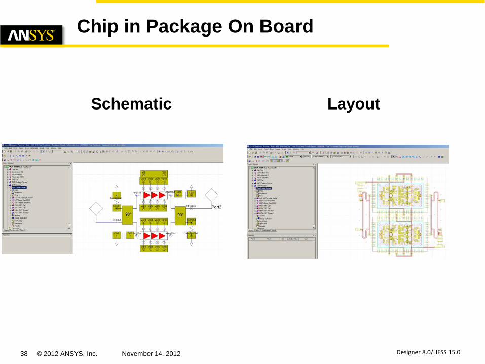
© 2012 ANSYS, Inc. Designer 8.0/HFSS 15.0 38 November 14, 2012
Chip in Package On Board
Schematic Layout

February 23, 2009 Inventory #002593
© 2012 ANSYS, Inc. Designer 8.0/HFSS 15.0 39 November 14, 2012
Chip in Package on Board (3D View)

February 23, 2009 Inventory #002593
© 2012 ANSYS, Inc. Designer 8.0/HFSS 15.0 40 November 14, 2012
Full Board Linear Performance
• System Gain very close to ideal: 21.9dB

February 23, 2009 Inventory #002593
© 2012 ANSYS, Inc. Designer 8.0/HFSS 15.0 41 November 14, 2012
The individual components will now be combined into a full assembly and analyzed in Designer using both HFSS for ECAD and circuit solvers simultaneously
• Simulating the full assembly
Part Four: The Full Assembly

February 23, 2009 Inventory #002593
© 2012 ANSYS, Inc. Designer 8.0/HFSS 15.0 42 November 14, 2012
Design Description
• Full System • Create a full system based on combining the
• 10 GHz VCO output • Dielectric resonator antennas • Balanced amplifiers
• Solve entire system in Designer to establish 10
GHz performance metrics that include • Bondwire effects • Vias and transitions effects • Layout effects • Coupling effects

February 23, 2009 Inventory #002593
© 2012 ANSYS, Inc. Designer 8.0/HFSS 15.0 43 November 14, 2012
Full Assembly Semi-ideal Schematic

February 23, 2009 Inventory #002593
© 2012 ANSYS, Inc. Designer 8.0/HFSS 15.0 44 November 14, 2012
Full Assembly Layout
RF Feed
Balanced Amplifiers
Antenna Feed
Antenna

February 23, 2009 Inventory #002593
© 2012 ANSYS, Inc. Designer 8.0/HFSS 15.0 45 November 14, 2012
Overview: Package to Board

February 23, 2009 Inventory #002593
© 2012 ANSYS, Inc. Designer 8.0/HFSS 15.0 46 November 14, 2012
Full Assembly Profile
69.2G RAM

February 23, 2009 Inventory #002593
© 2012 ANSYS, Inc. Designer 8.0/HFSS 15.0 47 November 14, 2012
• Multi-Processing – Single workstation solution to increase the speed of the solver
• Spectral Decomposition Method (SDM) – Accelerates frequency sweeps by distributing the spectral content
across a network of processors
High Performance Computing
#cores Clock Time Delta
Reference 1 10 hours 1X
HPC Interpolating with MP
8 2.5 hours 4X
HFSS – HPC-MT Processor Performance* Up to 5x faster solver.
4 Cores
8 Cores
2 Cores
1 Core 1x
1.9x
3.6x
5.6x
(Baseline) No HPC

February 23, 2009 Inventory #002593
© 2012 ANSYS, Inc. Designer 8.0/HFSS 15.0 48 November 14, 2012
Full Assembly Performance
• Amplifier Gain & Return Loss • Gain, Harmonics
8.0 8.5 9.0 9.5 10.0 10.5 11.0 11.5 12.0F [GHz]
-40
-30
-20
-10
0
10
20
S-Pa
ram
eter
s (d
B)
SAS IP, Inc. Power Amp Buildup2Amplifier S-Parameters
10.0055
-33.1085
16.1469
-21.4064
Curve InfodB(S(Port1,Port1))
LinearFrequencydB(S(Port2,Port1))
LinearFrequencydB(S(Port2,Port2))
LinearFrequency

February 23, 2009 Inventory #002593
© 2012 ANSYS, Inc. Designer 8.0/HFSS 15.0 49 November 14, 2012
Full Assembly Performance
• Spectral Output
0.00 25.00 50.00 75.00 100.00 125.00 150.00Spectrum [GHz]
-375.00
-250.00
-125.00
0.00
dBm
(P(P
ort2
))
Power Amp Buildup2Spectrum P2m1 Curve Info
dBm(P(Port2))HB1Tone
Name X Ym1 10.0000 -13.8290

February 23, 2009 Inventory #002593
© 2012 ANSYS, Inc. Designer 8.0/HFSS 15.0 50 November 14, 2012
Output Power at Typical Port
BLUE – Full Board RED – Single Amplifier
-20 -15 -10 -5 0 5 10 15 20Pinput, dBm [dBm]
-5
0
5
10
15
20
25
30
35
Pout,
dB
m
Power Amp Buildup2Pout Vs Pin PPT
m1
Curve InfoP_in_dBm
HB1Tone Sw eep
Name X Y
m1 11.0 27.2

February 23, 2009 Inventory #002593
© 2012 ANSYS, Inc. Designer 8.0/HFSS 15.0 51 November 14, 2012
Far Field Performance Comparison
Antenna Alone Antenna with Board

February 23, 2009 Inventory #002593
© 2012 ANSYS, Inc. Designer 8.0/HFSS 15.0 52 November 14, 2012
Far Field Performance Comparison
Antenna Alone Antenna with Board

February 23, 2009 Inventory #002593
© 2012 ANSYS, Inc. Designer 8.0/HFSS 15.0 53 November 14, 2012
Far Field Performance Comparison
Antenna Alone Antenna with Board

February 23, 2009 Inventory #002593
© 2012 ANSYS, Inc. Designer 8.0/HFSS 15.0 54 November 14, 2012
Concluding Remarks
• Designer can be used to simulate designs that are: – Large to very large – Extremely complex
• High bondwire counts, many vias, many transitions, include finite dielectrics
– Are a combination of electromagnetic and circuit simulation
• Designer can be used as a central design schematic into which various engineers or engineering teams provide input
• Designer with HFSS for ECAD is a tool that allows engineers of any level to gain access to the power of HFSS
• The new Cadence Integration allows engineers to remain in the Cadence design environment but solve their structure electromagnetically with HFSS in an easy and seamless manner