ANEXO AL TEMA 4 FÍSICA DEL ESTADO SÓLIDO II A_Tema_4A.pdf · 116 CHAPTER 4 The Semiconductor in...
13
ANEXO AL TEMA 4 FÍSICA DEL ESTADO SÓLIDO II
Transcript of ANEXO AL TEMA 4 FÍSICA DEL ESTADO SÓLIDO II A_Tema_4A.pdf · 116 CHAPTER 4 The Semiconductor in...
ANEXO AL TEMA 4 FÍSICA DEL ESTADO SÓLIDO II

BANDSTRUCTURE: SILICON
© Prof. Jasprit Singh www.eecs.umich.edu/~singh
Although the bandstructure of Si is far from ideal, having an indicrect bandgap, hig hhole masses, and small spin-orbit splitting, processing related advantages make Si the premier semiconductor for consumer electronics. On the right we show constant energy ellipsoids for Si conduction band. There are six equivalent valleys in Si at the bandedge.
6
5
4
3
2
1
0
–1
–2
–3–4
1.1
Eg
3.4
(a)(b)
kz
kx (100) (010)
(001)
(010) (100)
(001)ky
ENER
GY
(eV
)
Six equivalent valleys at conduction bandedge
Silicon
at 300K
Eg = 1.1eV
k
Eg = 1.17 – 4.37 x 10⁻⁴ T2
T – 636 (eV) T = Temperature in K
• Indirect gap material weak optical transitions, cannot be used to produce lasers.
• Valleys along the x-axis and –x-axis: k0x = (0.85,0,0) and k0x = (–0.85,0,0):2πa
2πa
(kx – k0x)2 kx + kzh22
E(k) = Ec +2 2
+ml * mt*
; ml = 0.98 m0; mt = 0.19 m0
similar E-k relations for other 4 valleys.
• Density of states mass = 1.08 m0 (6 valleys included).
• Heavy hole mass: 0.49 m0 ; light hole mass: 0.16 m0.
• Intrinsic carrier concentration at 300 K: 1.5 x 1010 cm–3.
ESTRUCTURA DE BANDAS E INTERVALO DE ENERGÍA PROHIBIDA PARA ALGUNOS SEMICONDUCTORES
BANDSTRUCTURE: SILICON
© Prof. Jasprit Singh www.eecs.umich.edu/~singh
Although the bandstructure of Si is far from ideal, having an indicrect bandgap, hig hhole masses, and small spin-orbit splitting, processing related advantages make Si the premier semiconductor for consumer electronics. On the right we show constant energy ellipsoids for Si conduction band. There are six equivalent valleys in Si at the bandedge.
6
5
4
3
2
1
0
–1
–2
–3–4
1.1
Eg
3.4
(a)(b)
kz
kx (100) (010)
(001)
(010) (100)
(001)ky
ENER
GY
(eV
)
Six equivalent valleys at conduction bandedge
Silicon
at 300K
Eg = 1.1eV
k
Eg = 1.17 – 4.37 x 10⁻⁴ T2
T – 636 (eV) T = Temperature in K
• Indirect gap material weak optical transitions, cannot be used to produce lasers.
• Valleys along the x-axis and –x-axis: k0x = (0.85,0,0) and k0x = (–0.85,0,0):2πa
2πa
(kx – k0x)2 kx + kzh22
E(k) = Ec +2 2
+ml * mt*
; ml = 0.98 m0; mt = 0.19 m0
similar E-k relations for other 4 valleys.
• Density of states mass = 1.08 m0 (6 valleys included).
• Heavy hole mass: 0.49 m0 ; light hole mass: 0.16 m0.
• Intrinsic carrier concentration at 300 K: 1.5 x 1010 cm–3.
BANDSTRUCTURE: GaAs
© Prof. Jasprit Singh www.eecs.umich.edu/~singh
The bandgap at 0 K is 1.51 eV and at 300 K it is 1.43 eV. The bottom of the conductionband is at k = (0,0,0), i.e., the G-point. The upper conduction band valleys are at the L-point.
Eg = 1.519 – 5.4 x 10⁻⁴ T2
T + 204 (eV)
CONDUCTION BAND: • Electron mass is light. m* = 0.067 m0 • Upper valley mass is large. m* = 0.25 m0 results in negative differential resistance at higher fields.• Material is direct bandgap and has strong optical transistions can be used for light emission.
VALENCE BAND: • Heavy hole mass: 0.45 m0; light hole mass = 0.08 m0. Intrinsic carrier concentration at 300 = 1.84 x 106 cm–3.
6
5
4
3
2
1
0
–1
–2
–3–4
0.3 0.58
CONDUCTION BAND
k
ENER
GY
(eV
)
Eg
Eg = 1.43eV at 300 K
Gallium Arsenide
[111] [100]
T = Temperature in K
BANDSTRUCTURE: Ge AlAs, InAs, InP
© Prof. Jasprit Singh www.eecs.umich.edu/~singh
(a) Bandstructure of Ge. (b) Bandstructure of AlAs. (c) Bandstructure of InAs. Since no adequate substitute matches InAs directly, it is often used as an alloy (InGaAs, InAlAs, etc.,) for devices. (d) Bandstructure of InP. InP is a very important material for high speed devices as well as a substrate and barrier layer material for semiconductor lasers.
(a) (b)
6
5
4
3
2
1
0
–1
–2
–3
–4L [111] Γ X[100]
ENER
GY
(e
V) Eg2.75
Eg = 2.15eV at 300K
0.3
0.90
L [111] Γ X[100]
ENER
GY
(e
V)
Eg
Aluminum ArsenideGermanium
Eg = 0.66eV
at 300K
6
5
4
3
2
1
0
–1
–2
–3
–4
(c) (d)
6
5
4
3
2
1
0
–1
–2
–3
–4L [111] Γ X[100]
ENER
GY
(e
V)
Eg
Indium Arsenide
k
Eg = 0.35eV
at 300K
0.69
0.94
L [111] Γ X[100]
ENER
GY
(e
V)
Eg
Indium Phosphide6
5
4
3
2
1
0
–1
–2
–3
–4
Eg = 1.34eV
at 300K
k
MASA EFECTIVA EN BANDA DE CONDUCCIÓN PARA SEMICONDUCTORES MÁS TÍPICOS
EFFECTIVE MASS DESCRIPTION
© Prof. Jasprit Singh www.eecs.umich.edu/~singh
CONDUCTION BAND: Direct bandgap material
Ec(k) = Ec(0) + h2k22m*c
with
The smaller the bandgap, the smaller the effective mass.
( )22pcvm*c
13
2 1+= +1m0
1EgΓ EgΓ + ∆m2
SPLIT-OFF BAND:Eso = –∆ – h2k2
2m*so
HEAVY HOLE; LIGHT HOLE:In a simple approximation the heavy hole and light hole bands can also be represented by masses m*hh and m* h. However, the real picture is more complex.
22pcvm*so
= +–1m0
13m2(EgΓ + ∆)
m*
mo
( )
CdSAlAsAlSb
GaPZnSe
ZnTe
CdSe
CdTeInPGaAs
GaSb
InAsInSb
0.2
0.1
0 1.0 2.0 3.00
Eg (eV)
EFFE
CTI
VE
MA
SS
BANDGAP
c
0
2pcv ~22 eVm0
2;
0
IBandadehuecosligerosIIBandahuecospesadosIIISplit-OffbandadeValencia𝛥 Split-Offenergía
Material Electron Hole Mass Mass(m0) (m0)
AlAs 0.1
AlSb 0.12 mdos = 0.98
GaN 0.19 mdos = 0.60
GaP 0.82 mdos = 0.60
GaAs 0.067 mlh = 0.082mhh = 0.45
GaSb 0.042 mdos = 0.40
Ge ml = 1.64 mlh = 0.044mt = 0.082 mhh = 0.28mdos= 0.56
InP 0.073 mdos = 0.64
InAs 0.027 mdos = 0.4
InSb 0.13 mdos = 0.4
Si ml = 0.98 mlh = 0.16mt = 0.19 mhh = 0.49
mdos= 1.08
Material Bandgap Relative(eV) Dielectric
Constant
C 5.5, I 5.57
Si 1.124, I 11.9
Ge 0.664, I 16.2
SiC 2.416, I 9.72
GaAs 1.424, D 13.18
AlAs 2.153, I 10.06
InAs 0.354, D 15.15
GaP 2.272, I 11.11
InP 1.344, D 12.56
InSb 0.230, D 16.8
CdTe 1.475, D 10.2
AlN 6.2, D 9.14
GaN 3.44, D 10.0
ZnSe 2.822, D 9.1
ZnTe 2.394, D 8.7
*
*
*
**
*
**
*
*
*
**
ELECTRONIC PROPERTIES OF SOME SEMICONDUCTORS
© Prof. Jasprit Singh www.eecs.umich.edu/~singh
Properties of some semiconductors. D and I stand for direct and indirect gap, respectively. The data are at 300 K. Note that Si has six conducton band valleys, while Ge has four.
Propiedadesdealgunossemiconductores.DeIindicantransicióndirectaeindirectarespectivamente.Losdatosmostradoscorrespondenconunatemperaturade300K.

Densidad de estados en bandade valencia y conducción yfunción de Fermi. Las áreasrepresentan la concentraciónde electrones y huecos en elcaso de que el nivel de Fermiesté en el centro del intervalode energía prohibida.Mostramos ampliación de laszonas cerca de los bordes debanda de valencia y banda deconducción.
108 CHAPTER 4 The Semiconductor in Equilibrium
semiconductor, then, electrons and holes are created in pairs by the thermal energy so that the number of electrons in the conduction band is equal to the number of holes in the valence band. Figure 4.1a shows a plot of the density of states function in the conduction-band gc(E), the density of states function in the valence-band gv(E), and the Fermi–Dirac probability function for T ! 0 K when EF is approximately halfway between Ec and Ev. If we assume, for the moment, that the electron and hole effective masses are equal, then gc(E) and gv(E) are symmetrical functions about the midgap energy (the energy midway between Ec and Ev). We noted previously that the function fF (E ) for E ! EF is symmetrical to the function 1 " fF (E) for E # EF about the energy E $ EF. This also means that the function fF(E) for E $ EF % dE is equal to the function 1 " fF (E ) for E $ EF " dE.
Figure 4.1 | (a) Density of states functions, Fermi–Dirac probability function, and areas representing electron and hole concentrations for the case when EF is near the midgap energy; (b) expanded view near the conduction-band energy; and (c) expanded view near the valence-band energy.
gc(E)fF(E) ! n(E)
Area ! n0 !electronconcentration
gv(E)(1 " fF(E)) ! p(E)
Area ! p0 !hole concentration
gc(E)
gv(E)
Ev
Ec
EF
E
fF(E) ! 0
fF(E)
fF(E) ! 1
(a)
(b)
(c)
gc(E)
Ec
fF(E)
0
gv(E)
Ev
[1 " fF(E)]
E
E
nea29583_ch04_106-155.indd 108nea29583_ch04_106-155.indd 108 12/11/10 10:10 AM12/11/10 10:10 AM
ELECTRONES Y HUECOS EN UN SEMICONDUCTOR INTRÍNSECO108 CHAPTER 4 The Semiconductor in Equilibrium
semiconductor, then, electrons and holes are created in pairs by the thermal energy so that the number of electrons in the conduction band is equal to the number of holes in the valence band. Figure 4.1a shows a plot of the density of states function in the conduction-band gc(E), the density of states function in the valence-band gv(E), and the Fermi–Dirac probability function for T ! 0 K when EF is approximately halfway between Ec and Ev. If we assume, for the moment, that the electron and hole effective masses are equal, then gc(E) and gv(E) are symmetrical functions about the midgap energy (the energy midway between Ec and Ev). We noted previously that the function fF (E ) for E ! EF is symmetrical to the function 1 " fF (E) for E # EF about the energy E $ EF. This also means that the function fF(E) for E $ EF % dE is equal to the function 1 " fF (E ) for E $ EF " dE.
Figure 4.1 | (a) Density of states functions, Fermi–Dirac probability function, and areas representing electron and hole concentrations for the case when EF is near the midgap energy; (b) expanded view near the conduction-band energy; and (c) expanded view near the valence-band energy.
gc(E)fF(E) ! n(E)
Area ! n0 !electronconcentration
gv(E)(1 " fF(E)) ! p(E)
Area ! p0 !hole concentration
gc(E)
gv(E)
Ev
Ec
EF
E
fF(E) ! 0
fF(E)
fF(E) ! 1
(a)
(b)
(c)
gc(E)
Ec
fF(E)
0
gv(E)
Ev
[1 " fF(E)]
E
E
nea29583_ch04_106-155.indd 108nea29583_ch04_106-155.indd 108 12/11/10 10:10 AM12/11/10 10:10 AM
108 CHAPTER 4 The Semiconductor in Equilibrium
semiconductor, then, electrons and holes are created in pairs by the thermal energy so that the number of electrons in the conduction band is equal to the number of holes in the valence band. Figure 4.1a shows a plot of the density of states function in the conduction-band gc(E), the density of states function in the valence-band gv(E), and the Fermi–Dirac probability function for T ! 0 K when EF is approximately halfway between Ec and Ev. If we assume, for the moment, that the electron and hole effective masses are equal, then gc(E) and gv(E) are symmetrical functions about the midgap energy (the energy midway between Ec and Ev). We noted previously that the function fF (E ) for E ! EF is symmetrical to the function 1 " fF (E) for E # EF about the energy E $ EF. This also means that the function fF(E) for E $ EF % dE is equal to the function 1 " fF (E ) for E $ EF " dE.
Figure 4.1 | (a) Density of states functions, Fermi–Dirac probability function, and areas representing electron and hole concentrations for the case when EF is near the midgap energy; (b) expanded view near the conduction-band energy; and (c) expanded view near the valence-band energy.
gc(E)fF(E) ! n(E)
Area ! n0 !electronconcentration
gv(E)(1 " fF(E)) ! p(E)
Area ! p0 !hole concentration
gc(E)
gv(E)
Ev
Ec
EF
E
fF(E) ! 0
fF(E)
fF(E) ! 1
(a)
(b)
(c)
gc(E)
Ec
fF(E)
0
gv(E)
Ev
[1 " fF(E)]
E
E
nea29583_ch04_106-155.indd 108nea29583_ch04_106-155.indd 108 12/11/10 10:10 AM12/11/10 10:10 AM
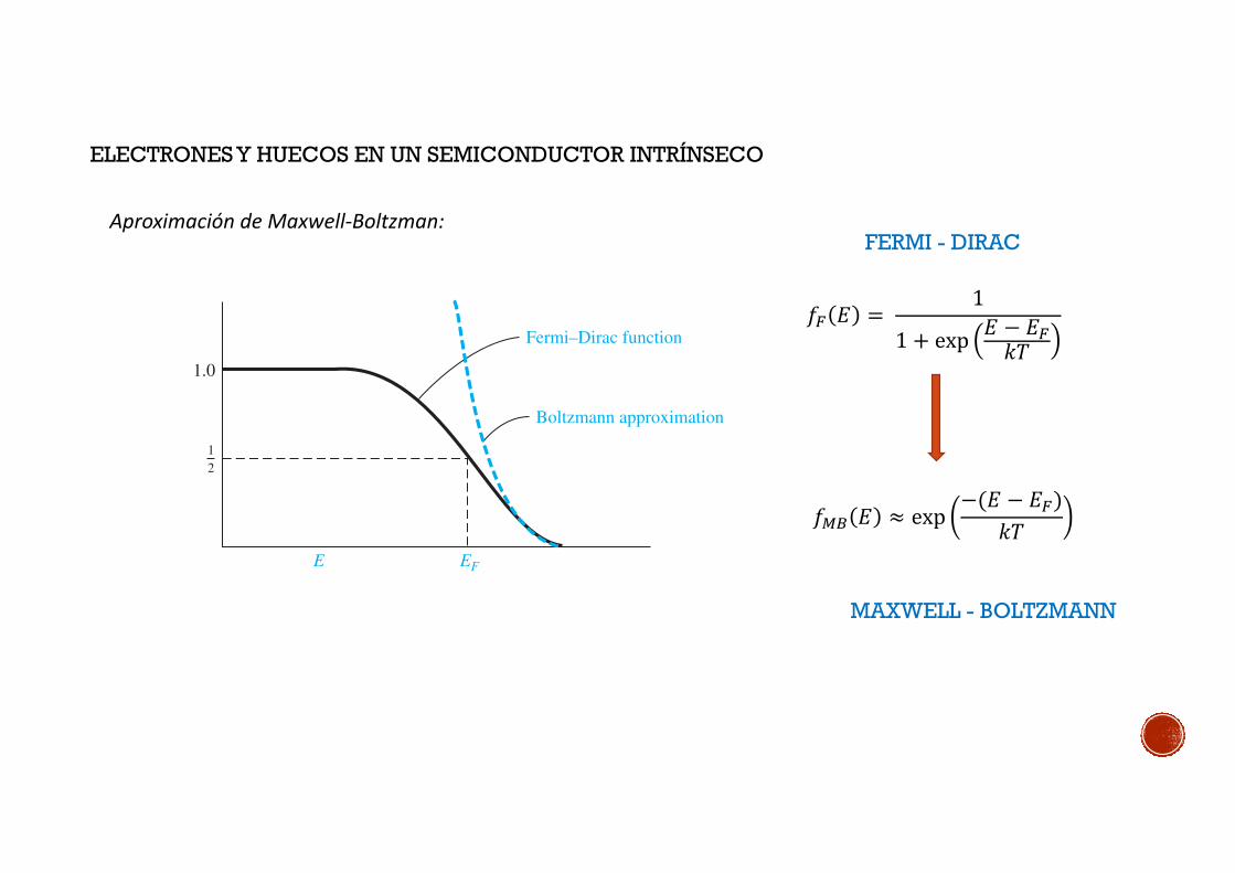
Aproximación de Maxwell-Boltzman:
ELECTRONES Y HUECOS EN UN SEMICONDUCTOR INTRÍNSECO
3.5 Statistical Mechanics 97
Fermi–Dirac function
Boltzmann approximation
1.0
12
E EF
Figure 3.35 | The Fermi–Dirac probability function and the Maxwell–Boltzmann approximation.
EXAMPLE 3.8 Objective: Determine the energy at which the Boltzmann approximation may be considered valid. Calculate the energy, in terms of kT and EF, at which the difference between the Boltzmann approximation and the Fermi–Dirac function is 5 percent of the Fermi function.
■ Solution We can write
exp ! !(E ! EF) __
kT " ! 1 ____
1 " exp # E ! EF __ kT
$
_______ 1 ____ 1 " exp # E ! EF __
kT $
# 0.05
If we multiply both numerator and denominator by the 1 " exp ( ) function, we have
exp ! !(E ! EF) __
kT " ! % 1 " exp ! E ! EF __
kT " & ! 1 # 0.05
which becomes
exp ! !(E ! EF) __
kT " # 0.05
or
(E ! EF) # kT ln # 1 _ 0.05 $ ' 3kT
■ Comment As seen in this example and in Figure 3.35 , the E ! E F ≫ kT notation is somewhat mislead-ing. The Maxwell–Boltzmann and Fermi–Dirac functions are within 5 percent of each other when E ! E F ' 3 kT .
■ EXERCISE PROBLEM Ex 3.8 Repeat Example 3.8 for the case when the difference between the Boltzmann
approximation and the Fermi–Dirac function is 2 percent of the Fermi function.
(Ans. E ! EF # 3.9kT)
nea29583_ch03_058-105.indd 97nea29583_ch03_058-105.indd 97 12/11/10 10:09 AM12/11/10 10:09 AM
𝑓# 𝐸 = 1
1 + exp 𝐸 − 𝐸#𝑘𝑇
𝑓/0 𝐸 ≈ exp−(𝐸 − 𝐸#)
𝑘𝑇
FERMI - DIRAC
MAXWELL - BOLTZMANN

En un semiconductor intrínseco y bajo la aproximación de Maxwell-Boltzman:
ELECTRONES Y HUECOS EN UN SEMICONDUCTOR INTRÍNSECO
𝑛 = 5 𝑔7 𝐸 𝑓# 𝐸 𝑑𝐸 ≈9
:;5 𝑔7 𝐸 𝑓/0 𝐸 𝑑𝐸 ≈ 2
2𝜋𝑚?∗𝑘𝑇ℎB
CBexp
−(𝐸D − 𝐸#)𝑘𝑇 = 𝑁7 exp
−(𝐸D − 𝐸#)𝑘𝑇
9
:;
𝑝 = 5 𝑔G 𝐸 (1 − 𝑓# 𝐸 )𝑑𝐸 ≈:H
I95 𝑔7 𝐸 (1 − 𝑓/0 𝐸 )𝑑𝐸 ≈ 2
2𝜋𝑚J∗ 𝑘𝑇ℎB
CBexp
−(𝐸# − 𝐸G)𝑘𝑇 =
:H
I9
𝑝 = 𝑁G exp−(𝐸# − 𝐸G)
𝑘𝑇
En todo semiconductor intrínseco n = p

Consecuencias:
ELECTRONES Y HUECOS EN UN SEMICONDUCTOR INTRÍNSECO
𝑛 = 𝑝 ⇒ 𝑁7 exp−(𝐸D − 𝐸#)
𝑘𝑇 = 𝑁G exp−(𝐸# − 𝐸G)
𝑘𝑇 ⇒ 𝑜𝑝𝑒𝑟𝑎𝑛𝑑𝑜
𝐸# = 12 𝐸G + 𝐸D +
12 𝑘𝑇𝐿𝑛
𝑁G𝑁D
=12 𝐸G + 𝐸D +
34 𝑘𝑇𝐿𝑛
𝑚S∗
𝑚?∗ ≈
12 𝐸G + 𝐸D =
12𝐸TUJ
𝑛 · 𝑝 = 𝑛WB = 𝑁D𝑁G exp−𝐸TUJ𝑘𝑇 = 𝑐𝑡𝑒.
𝑛W = 𝑝W = 4.826𝑥10B_ 𝑚?∗𝑚S
∗
𝑚?B
C/a
𝑇C/B exp−𝐸TUJ2𝑘𝑇 𝑚IC
Material ni (cm-3)
Si 1,5 x10¹⁰
GaAs 1,8 x10⁶
Ge 2,4 x10¹⁰

ELECTRONES Y HUECOS EN UN SEMICONDUCTOR INTRÍNSECO116 CHAPTER 4 The Semiconductor in Equilibrium
4.1.4 The Intrinsic Fermi-Level Position
We have qualitatively argued that the Fermi energy level is located near the center of the forbidden bandgap for the intrinsic semiconductor. We can specifi cally calcu-late the intrinsic Fermi-level position. Since the electron and hole concentrations are equal, setting Equations (4.20) and (4.21) equal to each other, we have
Nc exp ! !(Ec ! EFi) __ kT
" " Nv exp ! !(EFi ! Ev) __ kT
" (4.24)
Figure 4.2 | The intrinsic carrier concentration of Ge, Si, and GaAs as a function of temperature.(From Sze [14].)
0.5 1.0 1.5 2.0 2.5 3.0 3.5 4.0
1018
1019
15001000 500 200 100 27 0—20
T(•C)
Intr
insi
c ca
rrie
r den
sity
ni (
cm!
3 )
1000#T(K!1)
GaAs
Si
Ge
1017
1016
1015
1014
1013
1012
1011
1010
109
108
107
106
nea29583_ch04_106-155.indd 116nea29583_ch04_106-155.indd 116 12/11/10 10:10 AM12/11/10 10:10 AM
Concentración de portadores intrínsecosen diferentes semiconductores en funciónde la temperatura.
𝜎 total = ne𝜇? + 𝑝𝑒𝜇S =
= 4.826𝑥10B_ 𝑚?∗𝑚S
∗
𝑚?B
C/a
𝑇C/B𝑒 𝜇? + 𝜇S exp−𝐸TUJ2𝑘𝑇 =
= 773.1𝑚?∗𝑚S
∗
𝑚?B
C/a
𝑇C/B 𝜇? + 𝜇S exp−𝐸TUJ2𝑘𝑇
𝜎 total = 𝜎j exp−𝐸TUJ2𝑘𝑇

ELECTRONES Y HUECOS EN UN SEMICONDUCTOR INTRÍNSECO
El intervalo de energía prohibida depende delparámetro de red del material
𝜎 total = 𝜎j exp−𝐸TUJ2𝑘𝑇
T (!C)"50 0 50 100 150 200
1000
2000
5000
500
100
50
(a)
ND # 1014
ND # 1016
ND # 1017
ND # 1018
ND # 1019
!n
(cm
2 /V-s
)
T "2$2
ND # 1014 cm"3
100
500
1000
2000
4000
200 500 1000
!n
T (K)
T (!C)"50 0 50 100 150 200
1000
100
10
(b)
T "2$2
NA # 1014 cm"3
NA # 1016
NA # 1017
NA # 1018
NA # 1019
100100
200
500
1000
200 500 1000
!p
T (K)
!p
(cm
2 /V-s
)
NA # 1014
Figure 5.2 | (a) Electron and (b) hole mobilities in silicon versus temperature for various doping concentrations. Inserts show temperature dependence for “almost” intrinsic silicon. (From Pierret [8].)
16
2
nea29583_ch05_156-191.indd 162nea29583_ch05_156-191.indd 162
12/11/10 10:15 AM12/11/10 10:15 AM
T (!C)"50 0 50 100 150 200
1000
2000
5000
500
100
50
(a)
ND # 1014
ND # 1016
ND # 1017
ND # 1018
ND # 1019
!n
(cm
2 /V-s
)
T "2$2
ND # 1014 cm"3
100
500
1000
2000
4000
200 500 1000
!n
T (K)
T (!C)"50 0 50 100 150 200
1000
100
10
(b)
T "2$2
NA # 1014 cm"3
NA # 1016
NA # 1017
NA # 1018
NA # 1019
100100
200
500
1000
200 500 1000
!p
T (K)
!p
(cm
2 /V-s
)
NA # 1014
Figure 5.2 | (a) Electron and (b) hole mobilities in silicon versus temperature for various doping concentrations. Inserts show temperature dependence for “almost” intrinsic silicon. (From Pierret [8].)
162
nea29583_ch05_156-191.indd 162nea29583_ch05_156-191.indd 162
12/11/10 10:15 AM12/11/10 10:15 AM
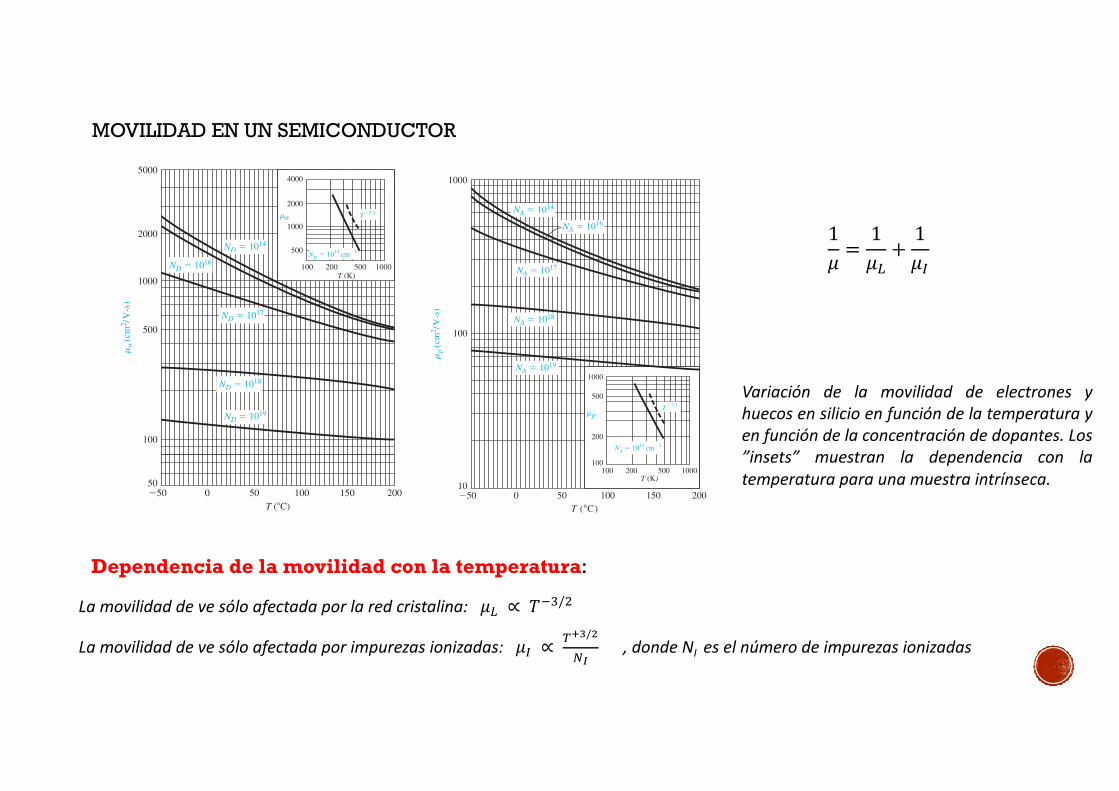
Variación de la movilidad de electrones yhuecos en silicio en función de la temperatura yen función de la concentración de dopantes. Los”insets” muestran la dependencia con latemperatura para una muestra intrínseca.
Dependencia de la movilidad con la temperatura:
La movilidad de ve sólo afectada por la red cristalina: 𝜇k ∝ 𝑇IC/B
La movilidad de ve sólo afectada por impurezas ionizadas: 𝜇m ∝ nop/q
rs, donde NI es el número de impurezas ionizadas
1𝜇 =
1𝜇k+1𝜇m
MOVILIDAD EN UN SEMICONDUCTOR

Variación de la movilidad de electrones yhuecos en silicio y germanio en función de laconcentración de impurezas.
MOVILIDAD EN UN SEMICONDUCTOR 5.1 Carrier Drift 163
If these two scattering processes are independent, then the total probability of a scatter-ing event occurring in the differential time dt is the sum of the individual events, or
dt _ ! ! dt _ !I " dt _ !L
(5.17)
where ! is the mean time between any scattering event. Comparing Equation (5.17) with the defi nitions of mobility given by Equation (5.13) or (5.14), we can write
1 _ " ! 1 _ "I " 1 _ "L
(5.18)
where "I is the mobility due to the ionized impurity scattering process and "L is the mobility due to the lattice scattering process. The parameter " is the net mobility. With two or more independent scattering mechanisms, the inverse mobilities add, which means that the net mobility decreases.
10191018101710161015
Impurity concentration (cm#3)
Mob
ility
(cm
2 /V-s
)
1014102
103
104
102
103
104
102
103
104
!n
!n
!n
!p
!p
!p
Ge
Si
T ! 300 K
GaAs
Figure 5.3 | Electron and hole mobilities versus impurity concentrations for germanium, silicon, and gallium arsenide at T ! 300 K. (From Sze [14].)
nea29583_ch05_156-191.indd 163nea29583_ch05_156-191.indd 163 12/11/10 10:15 AM12/11/10 10:15 AM

Relación entre la concentración de electrones yla conductividad en función del inverso de latemperatura en silicio.
𝜌 = 1𝜎 =
1𝑒 𝜇u𝑛 + 𝜇J𝑝
DEPENDENCIA DE LA RESISTIVIDAD CON LA TEMPERATURA EN UN SEMICONDUCTOR 5.1 Carrier Drift 167
We may plot the carrier concentration and conductivity of a semiconductor as a function of temperature for a particular doping concentration. Figure 5.6 shows the electron concentration and conductivity of silicon as a function of inverse tem-perature for the case when Nd ! 1015 cm"3. In the midtemperature range, or extrinsic range, as shown, we have complete ionization—the electron concentration remains essentially constant. However, the mobility is a function of temperature so the con-ductivity varies with temperature in this range. At higher temperatures, the intrinsic carrier concentration increases and begins to dominate the electron concentration as well as the conductivity. In the lower temperature range, freeze-out begins to occur; the electron concentration and conductivity decrease with decreasing temperature.
Figure 5.6 | Electron concentration and conductivity versus inverse temperature for silicon.(After Sze [14].)
Ele
ctro
n co
ncen
trat
ion
(cm
"3 )
Con
duct
ivity
(#–
cm)"
1
1000 300500
200 100 751017
1016 10
1.0
0.1
1015
1014
1013
0
n
ni
!
4 8 12 16 20
T (K)
(K"1)1000
T
EXAMPLE 5.3Objective: Determine the doping concentration and majority carrier mobility given the type and conductivity of a compensated semiconductor. Consider compensated n-type silicon at T ! 300 K, with a conductivity of ! !
16 (#-cm)"1 and an acceptor doping concentration of 1017 cm"3. Determine the donor concen-tration and the electron mobility.
■ SolutionFor n-type silicon at T ! 300 K, we can assume complete ionization; therefore the conductiv-ity, assuming Nd " Na ≫ ni, is given by
! ! e"n n ! e"n (Nd " Na)
We have that
16 ! (1.6 $ 10"19)"n(Nd " 1017)
nea29583_ch05_156-191.indd 167nea29583_ch05_156-191.indd 167 12/11/10 10:15 AM12/11/10 10:15 AM